Two-dimensional van der Waals materials View online:...
8
Two-dimensional van der Waals materials Pulickel Ajayan, Philip Kim, and Kaustav Banerjee Citation: Physics Today 69, 9, 38 (2016); doi: 10.1063/PT.3.3297 View online: http://dx.doi.org/10.1063/PT.3.3297 View Table of Contents: http://physicstoday.scitation.org/toc/pto/69/9 Published by the American Institute of Physics Articles you may be interested in The graphene–semiconductor Schottky junction Physics Today 69, 46 (2016); 10.1063/PT.3.3298 2D-2D tunneling field-effect transistors using WSe 2 /SnSe 2 heterostructures Applied Physics Letters 108, 083111 (2016); 10.1063/1.4942647 Band alignment of two-dimensional transition metal dichalcogenides: Application in tunnel field effect transistors Applied Physics Letters 103, 053513 (2013); 10.1063/1.4817409 Graphene and related two-dimensional materials: Structure-property relationships for electronics and optoelectronics Applied Physics Reviews 4, 021306 (2017); 10.1063/1.4983646 Substrate induced changes in atomically thin 2-dimensional semiconductors: Fundamentals, engineering, and applications Applied Physics Reviews 4, 011301 (2017); 10.1063/1.4974072 Band offsets and heterostructures of two-dimensional semiconductors Applied Physics Letters 102, 012111 (2013); 10.1063/1.4774090
Transcript of Two-dimensional van der Waals materials View online:...
Two-dimensional van der Waals materialsPulickel Ajayan, Philip Kim, and Kaustav Banerjee
Citation: Physics Today 69, 9, 38 (2016); doi: 10.1063/PT.3.3297View online: http://dx.doi.org/10.1063/PT.3.3297View Table of Contents: http://physicstoday.scitation.org/toc/pto/69/9Published by the American Institute of Physics
Articles you may be interested inThe graphene–semiconductor Schottky junctionPhysics Today 69, 46 (2016); 10.1063/PT.3.3298
2D-2D tunneling field-effect transistors using WSe2/SnSe2 heterostructuresApplied Physics Letters 108, 083111 (2016); 10.1063/1.4942647
Band alignment of two-dimensional transition metal dichalcogenides: Application in tunnel field effect transistorsApplied Physics Letters 103, 053513 (2013); 10.1063/1.4817409
Graphene and related two-dimensional materials: Structure-property relationships for electronics andoptoelectronicsApplied Physics Reviews 4, 021306 (2017); 10.1063/1.4983646
Substrate induced changes in atomically thin 2-dimensional semiconductors: Fundamentals, engineering, andapplicationsApplied Physics Reviews 4, 011301 (2017); 10.1063/1.4974072
Band offsets and heterostructures of two-dimensional semiconductorsApplied Physics Letters 102, 012111 (2013); 10.1063/1.4774090
Pulickel Ajayan, Philip Kim, and
Kaustav Banerjee
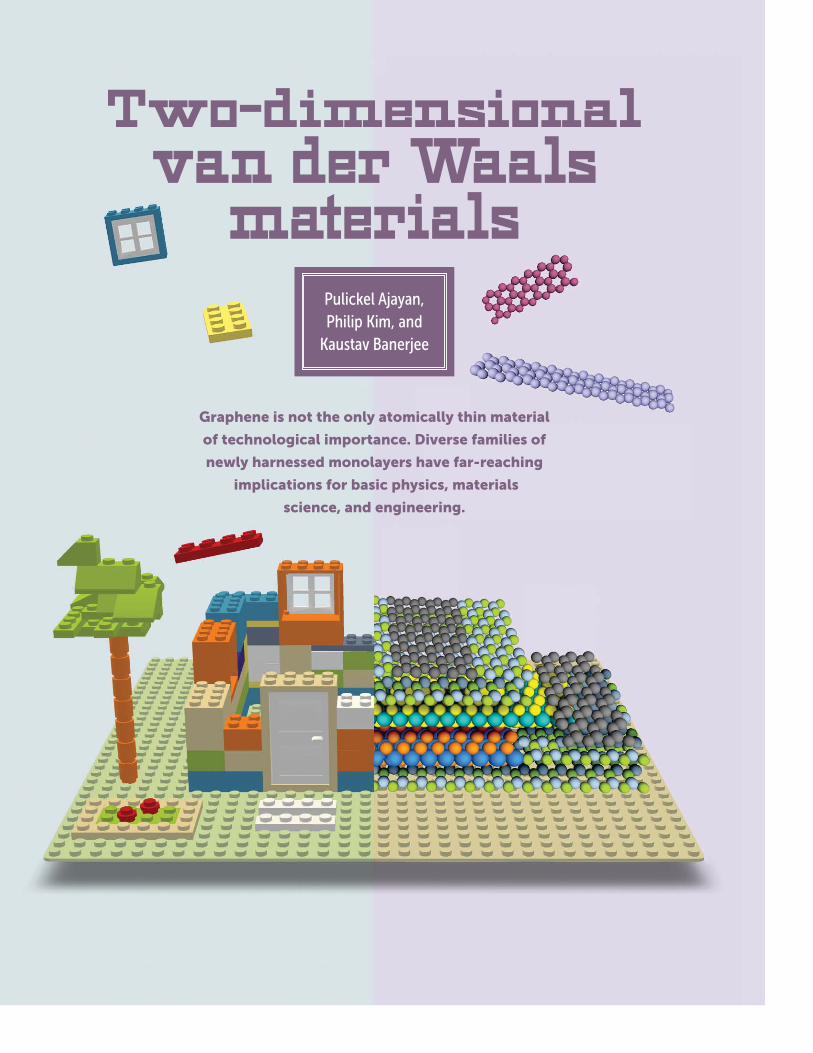
Graphene is not the only atomically thin material
of technological importance. Diverse families of
newly harnessed monolayers have far-reaching
implications for basic physics, materials
science, and engineering.
Two-dimensionalvan der Waals
materials
SEPTEMBER 2016 | PHYSICS TODAY 39
Pulickel Ajayan is a professor of materials science and nanoengineering at Rice University in Houston, Texas. Philip Kim is a professor of physics at Harvard University inCambridge, Massachusetts. Kaustav Banerjee is a professorof electrical and computer engineering at the University ofCalifornia, Santa Barbara.
Layered materials are characterized by extended crystallineplanar structures held together by strong in-plane covalent bondsand weak out-of-plane van der Waals forces. Individual layerscan easily be removed by breaking the van der Waals bonds,with little damage either to the remaining structure or to theextracted layer. For example, layers of graphene can be peeledaway from bulk graphite with adhesive tape. Hence layeredmaterials can be transferred to any substrate with relative ease.
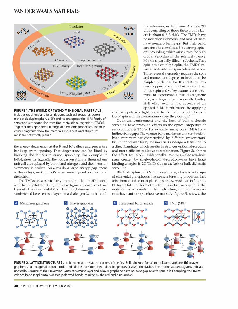
Graphene is one of the most alluring two-dimensional ma-terials because of its unique band structure and exceptionallyhigh carrier mobilities. (See the article by Andre Geim andAllan MacDonald, PHYSICS TODAY, August 2007, page 35.) Withthe discovery that graphene can be controllably grown onmetal surfaces by vapor-phase deposition from hydrocarbonprecursors, scalable graphene-based technologies started tolook more feasible.1 However, graphene is not the best 2D ma-terial for every application—its zero bandgap renders it ratheruseless as a semiconductor, for example. Fortunately, a largenumber of other layered materials span the entire spectrum ofelectronic properties, as shown in figure 1. Among them, hexag-onal boron nitride (h-BN) is an insulator with a bandgap ex-ceeding 5 eV, and the family of transition-metal dichalcogenides(TMDs) includes several semiconductors with bandgaps rang-ing from 0.5 eV to 3 eV. By exploiting the material propertiesof the layers in isolation or by mixing and matching them tocreate new structures with atomically thin heterojunctions, re-searchers are exploring interesting new physics and engineer-ing new ultrathin devices.
Physics in two dimensionsReducing the dimensionality of a system is often associatedwith exceptional electronic, optical, and magnetic properties,as the reduction of available phase space and diminished
screening lead to enhanced quantumeffects and increased correlations.Even before the discovery of stable 2Dmaterials, the condensed-matter com-munity extensively investigated thephysics of quasi-2D systems, includ-ing cuprate high-temperature super-conductors, whose superconductivityis confined to planar CuO2 layers, andsemiconductor interfaces that hostthe fractional quantum Hall effect.
The peculiar nature of low-dimensional systems is more appar-ent in atomically thin materials, and
indeed, graphene’s unique electronic properties stem from itsreduced dimensionality. The quantum mechanical descriptionof the electronic band structure can be simplified by introduc-ing quasi-relativistic particles near the corners of the Brillouinzone, as shown in figure 2a. At the Brillouin-zone corners,marked K and K’, the valence and conduction bands meet inconical valleys: Energy (represented by the vertical dimension)is directly proportional to momentum (represented by the hor-izontal dimensions), a relationship reminiscent of masslessparticles that travel at the speed of light, independent of theirenergy or momentum. Graphene’s quasiparticles thereforemove like electrons that have lost their mass, except that thespeed of light is replaced by graphene’s Fermi velocity, whichis some three hundred times smaller.
In real relativistic spin-1⁄2 fermions, such as neutrinos, thespin must be either parallel (right handed) or antiparallel (lefthanded) to the particle’s momentum. Graphene’s quasiparti-cles have an analogous pseudo-spin degree of freedom, whichdescribes the wavefunction symmetry on the two triangularsublattices of graphene’s hexagonal lattice: Depending onwhether the quasiparticle sits in a K or a K’ valley, the pseudospin is either parallel or antiparallel to the momentum. Fromthat chiral nature of charge carriers, various electronic proper-ties emerge, such as a half-integer shift in the quantum Hall effect and so-called Klein tunneling across an arbitrarily largepotential barrier. Graphene was also the first system in whicha nontrivial Berry phase could be detected experimentally, adiscovery that supplied an important connection to the laterdiscovery of topological insulators.2
In bilayer graphene, shown in figure 2b, two graphene lay-ers stack together to form a staggered honeycomb lattice. Itsquasiparticles gain a mass, and the energy dispersion becomesparabolic. The inversion symmetry of bilayer graphene keeps
What could we do with layered structureswith just the right layers?” asked RichardFeynman in his famous 1959 lecture,“There’s plenty of room at the bottom.”With the help of the amazing develop-
ments of the past several years, we are coming close to answering thatquestion. Whereas thin layers and multilayers of various kinds havelong been known to technology, researchers are now learning to create uniform, atomically thin layers and manipulate them into novelsolids with a broad range of physical properties.
‘‘
40 PHYSICS TODAY | SEPTEMBER 2016
VAN DER WAALS MATERIALS
the energy degeneracy at the K and K’ valleys and prevents abandgap from opening. That degeneracy can be lifted bybreaking the lattice’s inversion symmetry. For example, in h-BN, shown in figure 2c, the two carbon atoms in the grapheneunit cell are replaced by boron and nitrogen, and the inversionsymmetry is broken. As a result, a large energy gap opens at the valleys, making h-BN an extremely good insulator anddielectric.
The TMDs are a particularly interesting class of 2D materi-als. Their crystal structure, shown in figure 2d, consists of onelayer of a transition metal M, such as molybdenum or tungsten,sandwiched between two layers of a chalcogen X, such as sul-
fur, selenium, or tellurium. A single 2Dunit consisting of those three atomic lay-ers is about 6–8 Å thick. The TMDs haveno inversion symmetry, and most of themhave nonzero bandgaps. But their bandstructure is complicated by strong spin–orbit coupling, which arises from the highorbital velocities in the relatively heavy M atoms’ partially filled d subshells. Thatspin–orbit coupling splits the TMDs’ va-lence bands into two spin-polarized bands.Time-reversal symmetry requires the spinand momentum degrees of freedom to becoupled such that the K and K’ valleyscarry opposite spin polarizations. Thatunique spin and valley texture causes elec-trons to experience a pseudo-magneticfield, which gives rise to a so-called valleyHall effect even in the absence of an applied field. Furthermore, by applying
circularly polarized light, researchers can control both the elec-trons’ spin and the momentum valley they occupy.3
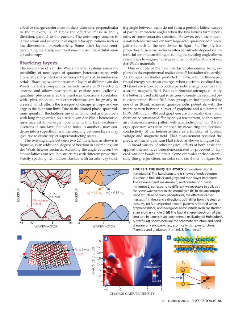
Quantum confinement and the lack of bulk dielectricscreening have profound effects on the optical properties ofsemiconducting TMDs. For example, many bulk TMDs haveindirect bandgaps: The valence-band maximum and conduction-band minimum are characterized by different wavevectors. But in monolayer form, the materials undergo a transition to a direct bandgap, which results in stronger optical absorptionand more efficient radiative recombination. Figure 3a showsthe effect for MoS2. Additionally, excitons—electron–hole pairs created by single-photon absorption—can have largebinding energies in 2D TMDs due to the lack of bulk dielectricscreening.
Black phosphorus (BP), or phosphorene, a layered allotropeof elemental phosphorus, has some interesting properties thatarise from its inherent in-plane anisotropy. As shown in figure 1,BP layers take the form of puckered sheets. Consequently, thematerial has an anisotropic band structure, and its charge car-riers have anisotropic effective mass. As figure 3b shows, the
FIGURE 1. THE WORLD OF TWO-DIMENSIONAL MATERIALSincludes graphene and its analogues, such as hexagonal boron nitride; black phosphorus (BP) and its analogues; the III–VI family ofsemiconductors; and the transition-metal dichalcogenides (TMDs).Together they span the full range of electronic properties. The fourcorner diagrams show the materials’ cross-sectional structures—most are not strictly planar.
FIGURE 2. LATTICE STRUCTURES and band structures at the corners of the first Brillouin zone for (a) monolayer graphene, (b) bilayergraphene, (c) hexagonal boron nitride, and (d) the transition-metal dichalcogenides (TMDs). The dashed lines in the lattice diagrams indicateunit cells. Because of their inversion symmetry, monolayer and bilayer graphene have no bandgap. Due to spin–orbit coupling, the TMDs’ valence band is split into two spin-polarized bands, marked by the red and blue arrows.
SEPTEMBER 2016 | PHYSICS TODAY 41
effective charge-carrier mass in the x direction, perpendicularto the puckers, is 12 times the effective mass in the ydirection, parallel to the puckers. The anisotropy couples to lattice strain and is being investigated for applications such aslow-dimensional piezoelectricity. Some other layered semi -conducting materials, such as rhenium disulfide, exhibit simi-lar anisotropy.
Stacking layersThe recent rise of van der Waals material systems raises thepossibility of new types of quantum heterostructures withatomically sharp interfaces between 2D layers of dissimilar ma-terials.4 Stacking two or more atomic layers of different van derWaals materials compounds the rich variety of 2D electronicsystems and allows researchers to explore novel collectivequantum phenomena at the interfaces. Electrons’ correlationwith spins, phonons, and other electrons can be greatly in-creased, which affects the transport of charge, entropy, and en-ergy in the quantum limit. Due to the limited phase-space vol-ume, quantum fluctuations are often enhanced and competewith long-range order. As a result, van der Waals heterostruc-tures may exhibit emergent phenomena: Interlayer excitons—electrons in one layer bound to holes in another—may con-dense into a superfluid, and the coupling between layers maygive rise to exotic triplet superconducting states.
The twisting angle between two 2D materials, as shown infigure 3c, is an additional degree of freedom in assembling vander Waals heterostructures: Adjusting the angle between twoatomic lattices can result in structures with different properties.Strictly speaking, two lattices stacked with an arbitrary twist-
ing angle between them do not form a periodic lattice, exceptat particular discrete angles when the two lattices form a peri-odic, or commensurate, structure. However, even incommen-surate heterostructures can form large-scale quasi-periodic moirépatterns, such as the one shown in figure 3c. The physicalproperties of heterostructures often sensitively depend on in-terfacial commensurability, so tuning the twisting angle allowsresearchers to engineer a large number of combinations of vander Waals materials.
One example of the new interfacial phenomena being ex-plored is the experimental realization of Hofstadter’s butterfly.5
As Douglas Hofstadter predicted in 1976, a butterfly-shapedfractal energy spectrum emerges when electrons confined to a2D sheet are subjected to both a periodic energy potential anda strong magnetic field. Past experimental attempts to studythe butterfly used artificial structures to create the required pe-riodic potential. But in 2013 three groups, including one led byone of us (Kim), achieved quasi-periodic potentials with themoiré pattern between a layer of graphene and a substrate ofh-BN. Although h-BN and graphene are atomically dissimilar,their lattice constants differ by only a few percent, so they forman atomic-scale moiré pattern with a periodic potential. The en-ergy spectrum was then mapped by measuring the electricalconductivity of the heterostructure as a function of appliedvoltage and magnetic field. That measurement revealed thepredicted fractal quantum Hall effect, as shown in figure 3d.
A broad variety of other physical effects of both basic andapplied interest have been demonstrated or proposed in lay-ered van der Waals materials. Some examples include atomi-cally thin p–n junctions for solar cells (as shown in figure 3e),
FIGURE 3. THE UNIQUE PHYSICS of two-dimensional materials. (a) The band structure is shown of molybdenumdisulfide in bulk (black and gray) and monolayer (red) forms. The valence-band maximum Ev and conduction-band minimum Ec correspond to different wavevectors in bulk butthe same wavevector in the monolayer. (b) In the anisotropicband structure of black phosphorus, the effective carrier masses m* in the x and y directions both differ from the electronmass m0. (c) A quasiperiodic moiré pattern is formed whengraphene (black) and hexagonal boron nitride (red) are stackedat an arbitrary angle θ. (d) The fractal energy spectrum of thestructure in panel c is an experimental realization of Hofstadter’sbutterfly. (e) Shown here are the schematic structure and banddiagram of a photoexcited, atomically thin p–n junction. (Panels c and d adapted from ref. 5, Dean et al.)
42 PHYSICS TODAY | SEPTEMBER 2016
VAN DER WAALS MATERIALS
exciton superfluidity at high temperatures,6 novel chiral reso-nant tunneling between misaligned graphene sheets separatedby a h-BN barrier,7 and superconductor–semiconductor inter-faces with unusual Andreev reflections and Josephson coupling.
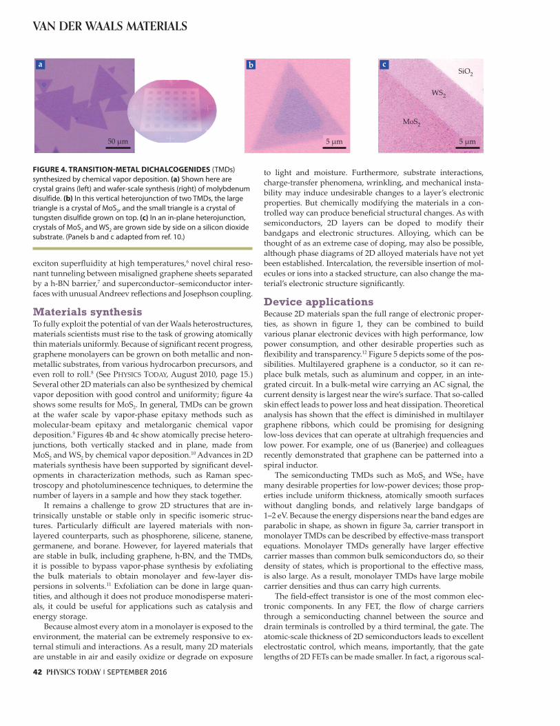
Materials synthesisTo fully exploit the potential of van der Waals heterostructures,materials scientists must rise to the task of growing atomicallythin materials uniformly. Because of significant recent progress,graphene monolayers can be grown on both metallic and non-metallic substrates, from various hydrocarbon precursors, andeven roll to roll.8 (See PHYSICS TODAY, August 2010, page 15.)Several other 2D materials can also be synthesized by chemicalvapor deposition with good control and uniformity; figure 4ashows some results for MoS2. In general, TMDs can be grownat the wafer scale by vapor-phase epitaxy methods such as molecular-beam epitaxy and metalorganic chemical vapordeposition.9 Figures 4b and 4c show atomically precise hetero-junctions, both vertically stacked and in plane, made fromMoS2 and WS2 by chemical vapor deposition.10 Advances in 2Dmaterials synthesis have been supported by significant devel-opments in characterization methods, such as Raman spec-troscopy and photoluminescence techniques, to determine thenumber of layers in a sample and how they stack together.
It remains a challenge to grow 2D structures that are in -trinsically unstable or stable only in specific isomeric struc-tures. Particularly difficult are layered materials with non -layered counterparts, such as phosphorene, silicene, stanene,germanene, and borane. However, for layered materials thatare stable in bulk, including graphene, h-BN, and the TMDs, it is possible to bypass vapor-phase synthesis by exfoliating the bulk materials to obtain monolayer and few-layer dis -persions in solvents.11 Exfoliation can be done in large quan -tities, and although it does not produce monodisperse materi-als, it could be useful for applications such as catalysis andenergy storage.
Because almost every atom in a monolayer is exposed to theenvironment, the material can be extremely responsive to ex-ternal stimuli and interactions. As a result, many 2D materialsare unstable in air and easily oxidize or degrade on exposure
to light and moisture. Furthermore, substrate interactions,charge-transfer phenomena, wrinkling, and mechanical insta-bility may induce undesirable changes to a layer’s electronicproperties. But chemically modifying the materials in a con-trolled way can produce beneficial structural changes. As withsemiconductors, 2D layers can be doped to modify theirbandgaps and electronic structures. Alloying, which can bethought of as an extreme case of doping, may also be possible,although phase diagrams of 2D alloyed materials have not yetbeen established. Intercalation, the reversible insertion of mol-ecules or ions into a stacked structure, can also change the ma-terial’s electronic structure significantly.
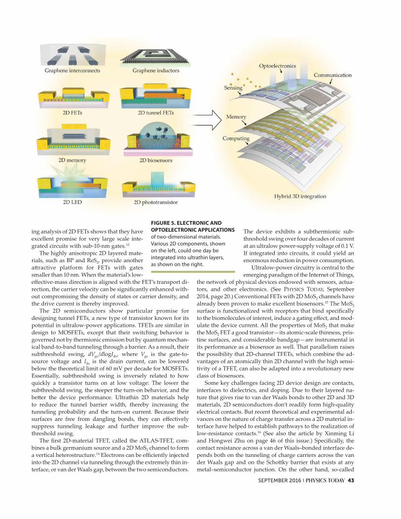
Device applicationsBecause 2D materials span the full range of electronic proper-ties, as shown in figure 1, they can be combined to build various planar electronic devices with high performance, lowpower consumption, and other desirable properties such asflexibility and transparency.12 Figure 5 depicts some of the pos-sibilities. Multilayered graphene is a conductor, so it can re-place bulk metals, such as aluminum and copper, in an inte-grated circuit. In a bulk-metal wire carrying an AC signal, thecurrent density is largest near the wire’s surface. That so-calledskin effect leads to power loss and heat dissipation. Theoreticalanalysis has shown that the effect is diminished in multilayergraphene ribbons, which could be promising for designinglow-loss devices that can operate at ultrahigh frequencies andlow power. For example, one of us (Banerjee) and colleaguesrecently demonstrated that graphene can be patterned into aspiral inductor.
The semiconducting TMDs such as MoS2 and WSe2 havemany desirable properties for low-power devices; those prop-erties include uniform thickness, atomically smooth surfaceswithout dangling bonds, and relatively large bandgaps of 1–2 eV. Because the energy dispersions near the band edges areparabolic in shape, as shown in figure 3a, carrier transport inmonolayer TMDs can be described by effective-mass transportequations. Monolayer TMDs generally have larger effectivecarrier masses than common bulk semiconductors do, so theirdensity of states, which is proportional to the effective mass, is also large. As a result, monolayer TMDs have large mobilecarrier densities and thus can carry high currents.
The field-effect transistor is one of the most common elec-tronic components. In any FET, the flow of charge carriersthrough a semiconducting channel between the source anddrain terminals is controlled by a third terminal, the gate. Theatomic-scale thickness of 2D semiconductors leads to excellentelectrostatic control, which means, importantly, that the gatelengths of 2D FETs can be made smaller. In fact, a rigorous scal-
FIGURE 4. TRANSITION-METAL DICHALCOGENIDES (TMDs) synthesized by chemical vapor deposition. (a) Shown here are crystal grains (left) and wafer-scale synthesis (right) of molybdenumdisulfide. (b) In this vertical heterojunction of two TMDs, the largetriangle is a crystal of MoS2, and the small triangle is a crystal oftungsten disulfide grown on top. (c) In an in-plane heterojunction,crystals of MoS2 and WS2 are grown side by side on a silicon dioxidesubstrate. (Panels b and c adapted from ref. 10.)
SEPTEMBER 2016 | PHYSICS TODAY 43
ing analysis of 2D FETs shows that they haveexcellent promise for very large scale inte-grated circuits with sub-10-nm gates.13
The highly anisotropic 2D layered mate-rials, such as BP and ReS2, provide anotherattractive platform for FETs with gatessmaller than 10 nm. When the material’s low-effective-mass direction is aligned with the FET’s transport di-rection, the carrier velocity can be significantly enhanced with-out compromising the density of states or carrier density, andthe drive current is thereby improved.
The 2D semiconductors show particular promise for designing tunnel FETs, a new type of transistor known for itspotential in ultralow-power applications. TFETs are similar indesign to MOSFETs, except that their switching behavior isgoverned not by thermionic emission but by quantum mechan-ical band-to-band tunneling through a barrier. As a result, theirsubthreshold swing, dVgs/dlogIds, where Vgs is the gate-to-source voltage and Ids is the drain current, can be loweredbelow the theoretical limit of 60 mV per decade for MOSFETs.Essentially, subthreshold swing is inversely related to howquickly a transistor turns on at low voltage: The lower the subthreshold swing, the steeper the turn-on behavior, and thebetter the device performance. Ultrathin 2D materials help to reduce the tunnel barrier width, thereby increasing the tunneling probability and the turn-on current. Because theirsurfaces are free from dangling bonds, they can effectively suppress tunneling leakage and further improve the sub-threshold swing.
The first 2D-material TFET, called the ATLAS-TFET, com-bines a bulk germanium source and a 2D MoS2 channel to forma vertical heterostructure.14 Electrons can be efficiently injectedinto the 2D channel via tunneling through the extremely thin in-terface, or van der Waals gap, between the two semiconductors.
The device exhibits a subthermionic sub-threshold swing over four decades of currentat an ultralow power-supply voltage of 0.1 V.If integrated into circuits, it could yield anenormous reduction in power consumption.
Ultralow-power circuitry is central to theemerging paradigm of the Internet of Things,
the network of physical devices endowed with sensors, actua-tors, and other electronics. (See PHYSICS TODAY, September2014, page 20.) Conventional FETs with 2D MoS2 channels havealready been proven to make excellent biosensors.15 The MoS2
surface is functionalized with receptors that bind specificallyto the biomolecules of interest, induce a gating effect, and mod-ulate the device current. All the properties of MoS2 that makethe MoS2 FET a good transistor—its atomic-scale thinness, pris-tine surfaces, and considerable bandgap—are instrumental inits performance as a biosensor as well. That parallelism raisesthe possibility that 2D-channel TFETs, which combine the ad-vantages of an atomically thin 2D channel with the high sensi-tivity of a TFET, can also be adapted into a revolutionary newclass of biosensors.
Some key challenges facing 2D device design are contacts,interfaces to dielectrics, and doping. Due to their layered na-ture that gives rise to van der Waals bonds to other 2D and 3Dmaterials, 2D semiconductors don’t readily form high-qualityelectrical contacts. But recent theoretical and experimental ad-vances on the nature of charge transfer across a 2D material in-terface have helped to establish pathways to the realization oflow-resistance contacts.16 (See also the article by Xinming Liand Hongwei Zhu on page 46 of this issue.) Specifically, thecontact resistance across a van der Waals–bonded interface de-pends both on the tunneling of charge carriers across the vander Waals gap and on the Schottky barrier that exists at anymetal–semiconductor junction. On the other hand, so-called
FIGURE 5. ELECTRONIC AND OPTOELECTRONIC APPLICATIONSof two-dimensional materials. Various 2D components, shown on the left, could one day be integrated into ultrathin layers, as shown on the right.

VAN DER WAALS MATERIALS
seamless electrical contacts, such as the covalently bonded in-plane interfaces between different 2D materials, provide apromising way to lower contact resistances.
Feynman’s dream come trueAtomically thin materials have the potential to revolutionizetechnologies from nanoelectronics to optoelectronics and fromcatalysis to coatings. The ability to control the electronic statesof 2D materials is expected to lead to new physical phenomenaand device concepts. Furthermore, stable atomic monolayerswith various compositions and electronic structures can bestacked in combinatorial ways to produce a large number oflayered material systems with as yet unexplored properties.Semiconducting 2D monolayers with direct bandgaps are ide-ally suited for generating and detecting photons at wave-lengths that vary as a function of the bandgaps, which can betuned through composition, chemistry, or quantum confine-ment. The confinement could be achieved simply by changingthe number of layers, provided that the materials can be syn-thesized and characterized with atomic precision.
Looking ahead, integration of various 2D circuit elementsinto 2D logic and memory circuits could be an attractive wayto create ultradense, low-power, flexible electronics. It may evenbe possible to form entire logic circuits from a monolithic sheetof a single starting material—such as graphene, which can beturned from a conductor into a semiconductor either by dopingor by patterning it into armchair nanoribbons—and thereby al-leviate the need for external contacts.17 Furthermore, 2D logicand memory layers could be vertically integrated with 2D op-
tics, sensors, and components for energy scavenging and stor-age, as schematically depicted in the right panel of figure 5, toform compact, energy-efficient devices of ultimate thinness.We are coming ever closer to realizing Feynman’s dream of lay-ered materials—and devices—with just the right layers.
We thank Jiahao Kang of the Nanoelectronics Research Lab at the University of California, Santa Barbara for his assistance in drawingsome of the figures.
REFERENCES1. X. Li et al., Science 324, 1312 (2009).2. C. L. Kane, E. J. Mele, Phys. Rev. Lett. 95, 226801 (2005). 3. D. Xiao et al., Phys. Rev. Lett. 108, 196802 (2012).4. A. K. Geim, I. Grigorieva, Nature 499, 419 (2013).5. C. R. Dean et al., Nature 497, 598 (2013); L. A. Ponomarenko et al.,
Nature 497, 594 (2013); B. Hunt et al., Science 340, 1427 (2013).6. M. M. Fogler, L. V. Butov, K. S. Novoselov, Nat. Commun. 5, 4555
(2014).7. M. T. Greenaway et al., Nat. Phys. 11, 1057 (2015).8. S. Bae et al., Nat. Nanotechnol. 5, 574 (2010).9. K. Kang et al., Nature 520, 656 (2015).
10. Y. Gong et al., Nat. Mater. 13, 1135 (2014).11. V. Nicolosi et al., Science 340, 1420 (2013).12. D. Akinwande, N. Petrone, J. Hone, Nat. Commun. 5, 5678 (2014);
G. Fiori et al., Nat. Nanotechnol. 9, 768 (2014).13. W. Cao et al., IEEE Trans. Electron. Devices 62, 3459 (2015).14. D. Sarkar et al., Nature 526, 91 (2015).15. D. Sarkar et al., ACS Nano 8, 3992 (2014).16. A. Allain et al., Nat. Mater. 14, 1195 (2015); J. Kang et al., Phys.
Rev. X 4, 031005 (2014).17. J. Kang et al., Appl. Phys. Lett. 103, 083113 (2013). PT
www.mdcvacuum.com800.443.8817 | [email protected]
From bottle to process in one simple step.
MFC GAS STICK
New! XpressStick™ ISO9001:2008M
DC
Vac
uum
Products, LLC ISO
Certified M
DC
Vac
uum
Products, LLC ISO
Certified
ORDER ONLINE!