Two-dimensional semiconductor device simulation of...
10
IEEE TRANSACTIONS ON ELECTRON DEVICES, VOL. 50, NO. 5,MAY 2003 1353 Two-Dimensional Semiconductor Device Simulation of Trap-Assisted Generation-Recombination Noise Under Periodic Large-Signal Conditions and Its Use for Developing Cyclostationary Circuit Simulation Models Juan E. Sanchez, Member, IEEE, Gijs Bosman, Senior Member, IEEE, and Mark E. Law, Fellow, IEEE Abstract—The simulation of generation-recombination (GR) noise under periodic large-signal conditions in a partial differen- tial equation-based silicon device simulator is presented. Using the impedance-field method with cyclostationary noise sources, it is possible to simulate the self- and cross-spectral densities between sidebands of a periodic large-signal stimulus. Such information is needed to develop noise correlation matrices for use with a circuit simulator. Examples are provided which demonstrate known results for shot noise in bipolar junction transistors. Additional results demonstrate the upconversion of low-frequency GR noise for microscopically cyclostationary noise sources and provide evidence for applying the modulated stationary noise model for low-frequency noise when there is a nearly quadratic current dependence. Index Terms—Correlation, frequency conversion, mixer noise, nonlinear circuits, nonlinear systems, semiconductor device mod- eling, semiconductor device noise. I. INTRODUCTION T HE FREQUENCY conversion of noise under periodic large-signal conditions is of active interest to both the device physics and circuit design communities [1], [2]. It has a significant effect on the performance of wireless communica- tions circuits, such as the spectral purity of oscillators and the noise figure of mixers. While the conversion of shot and thermal noise is well under- stood and has successfully been modeled for circuit simulation using noise correlation matrices (NCMs) [3], [4], the modula- tion of -like low-frequency noise is still an open topic [5], [6]. This is, in part, due to the fact that such low-frequency noise can be attributed to a variety of sources [7]. In addition, the con- tribution of such noise sources is dependent on its spatial loca- tion and the unknown time-varying bias dependence of their au- tocorrelation. Manuscript received November 4, 2002; revised January 22, 2003. This work was supported by the Semiconductor Research Corporation (SRC). The review of this paper was arranged by Editor J. Deen. J. E. Sanchez was with the Department of Electrical and Computer Engi- neering, University of Florida, Gainesville, FL 32611 USA. He is now with Synopsys, Inc., Mountain View, CA 94043 USA (e-mail: [email protected]). G. Bosman and M. E. Law are with the Department of Electrical and Com- puter Engineering, University of Florida, Gainesville, FL 32611 USA. Digital Object Identifier 10.1109/TED.2003.813448 The impedance field method (IFM) originally referred to the coupling of current-density (velocity) fluctuations within the semiconductor to an open-circuit voltage at the contacts of the device [8]. This method was typically used to get analytic re- sults for both velocity fluctuation and generation-recombina- tion (GR) transition-rate fluctuations [9]. The IFM was extended to partial differential equation (PDE)-based semiconductor de- vice simulation [10]. These techniques were then extrapolated for the case of device simulation of cyclostationary noise under periodic steady-state conditions [1], [11]. In [12], the authors present simulation results for microscopically cyclostationary trap-assisted GR noise sources. The drift-diffusion simulation of semiconductor devices re- quires the solution of the Poisson, electron-continuity, and hole- continuity equations for each differential volume within a semi- conductor mesh. In order to consider an indirect recombination or trapping process which results in frequency-dependent noise, it is also necessary to consider a trap-continuity equation. The Florida object-oriented device simulator (FLOODS) [13], [14] has been enhanced with noise simulation capability for one-di- mensional (1-D) and two-dimensional (2-D) semiconductor de- vices under both dc and periodic time-varying bias conditions. This tool is capable of solving for an arbitrary number of user- defined PDEs. In addition, the auto- and cross correlation of the Langevin terms of the IFM are specified for each PDE. As a re- search tool, this software is being used to investigate both GR and diffusion noise and the resulting effect on the device perfor- mance in silicon. In Section II, we review the IFM generalized to periodic large-signal conditions. The modulated stationary noise model is applied for the case of trap-assisted GR noise. Section III presents the NCM, which is used in circuit simulation to model cyclostationary equivalent current noise sources. We discuss how the NCM can be extracted through semiconductor device simulation. We then develop the NCM model for the case of microscopically stationary GR noise for comparison with simulation results. In Section IV, simulation results are presented for the fre- quency conversion of both diffusion noise and trap-assisted GR noise under periodic large-signal conditions for a bipolar junc- tion transistor (BJT). While the focus of this paper is on GR 0018-9383/03$17.00 © 2003 IEEE
-
Upload
nguyennhan -
Category
Documents
-
view
213 -
download
0
Transcript of Two-dimensional semiconductor device simulation of...

IEEE TRANSACTIONS ON ELECTRON DEVICES, VOL. 50, NO. 5, MAY 2003 1353
Two-Dimensional Semiconductor Device Simulationof Trap-Assisted Generation-RecombinationNoise Under Periodic Large-Signal Conditionsand Its Use for Developing Cyclostationary
Circuit Simulation ModelsJuan E. Sanchez, Member, IEEE, Gijs Bosman, Senior Member, IEEE, and Mark E. Law, Fellow, IEEE
Abstract—The simulation of generation-recombination (GR)noise under periodic large-signal conditions in a partial differen-tial equation-based silicon device simulator is presented. Using theimpedance-field method with cyclostationary noise sources, it ispossible to simulate the self- and cross-spectral densities betweensidebands of a periodic large-signal stimulus. Such information isneeded to develop noise correlation matrices for use with a circuitsimulator. Examples are provided which demonstrate knownresults for shot noise in bipolar junction transistors. Additionalresults demonstrate the upconversion of low-frequency GR noisefor microscopically cyclostationary noise sources and provideevidence for applying the modulated stationary noise model forlow-frequency noise when there is a nearly quadratic currentdependence.
Index Terms—Correlation, frequency conversion, mixer noise,nonlinear circuits, nonlinear systems, semiconductor device mod-eling, semiconductor device noise.
I. INTRODUCTION
THE FREQUENCY conversion of noise under periodiclarge-signal conditions is of active interest to both the
device physics and circuit design communities [1], [2]. It has asignificant effect on the performance of wireless communica-tions circuits, such as the spectral purity of oscillators and thenoise figure of mixers.While the conversion of shot and thermal noise is well under-
stood and has successfully been modeled for circuit simulationusing noise correlation matrices (NCMs) [3], [4], the modula-tion of -like low-frequency noise is still an open topic [5],[6]. This is, in part, due to the fact that such low-frequency noisecan be attributed to a variety of sources [7]. In addition, the con-tribution of such noise sources is dependent on its spatial loca-tion and the unknown time-varying bias dependence of their au-tocorrelation.
Manuscript received November 4, 2002; revised January 22, 2003. This workwas supported by the Semiconductor Research Corporation (SRC). The reviewof this paper was arranged by Editor J. Deen.J. E. Sanchez was with the Department of Electrical and Computer Engi-
neering, University of Florida, Gainesville, FL 32611 USA. He is now withSynopsys, Inc., Mountain View, CA 94043 USA (e-mail: [email protected]).G. Bosman and M. E. Law are with the Department of Electrical and Com-
puter Engineering, University of Florida, Gainesville, FL 32611 USA.Digital Object Identifier 10.1109/TED.2003.813448
The impedance field method (IFM) originally referred to thecoupling of current-density (velocity) fluctuations within thesemiconductor to an open-circuit voltage at the contacts of thedevice [8]. This method was typically used to get analytic re-sults for both velocity fluctuation and generation-recombina-tion (GR) transition-rate fluctuations [9]. The IFMwas extendedto partial differential equation (PDE)-based semiconductor de-vice simulation [10]. These techniques were then extrapolatedfor the case of device simulation of cyclostationary noise underperiodic steady-state conditions [1], [11]. In [12], the authorspresent simulation results for microscopically cyclostationarytrap-assisted GR noise sources.The drift-diffusion simulation of semiconductor devices re-
quires the solution of the Poisson, electron-continuity, and hole-continuity equations for each differential volume within a semi-conductor mesh. In order to consider an indirect recombinationor trapping process which results in frequency-dependent noise,it is also necessary to consider a trap-continuity equation. TheFlorida object-oriented device simulator (FLOODS) [13], [14]has been enhanced with noise simulation capability for one-di-mensional (1-D) and two-dimensional (2-D) semiconductor de-vices under both dc and periodic time-varying bias conditions.This tool is capable of solving for an arbitrary number of user-defined PDEs. In addition, the auto- and cross correlation of theLangevin terms of the IFM are specified for each PDE. As a re-search tool, this software is being used to investigate both GRand diffusion noise and the resulting effect on the device perfor-mance in silicon.In Section II, we review the IFM generalized to periodic
large-signal conditions. The modulated stationary noise modelis applied for the case of trap-assisted GR noise. Section IIIpresents the NCM, which is used in circuit simulation to modelcyclostationary equivalent current noise sources. We discusshow the NCM can be extracted through semiconductor devicesimulation. We then develop the NCM model for the caseof microscopically stationary GR noise for comparison withsimulation results.In Section IV, simulation results are presented for the fre-
quency conversion of both diffusion noise and trap-assisted GRnoise under periodic large-signal conditions for a bipolar junc-tion transistor (BJT). While the focus of this paper is on GR
0018-9383/03$17.00 © 2003 IEEE
1354 IEEE TRANSACTIONS ON ELECTRON DEVICES, VOL. 50, NO. 5, MAY 2003
noise, diffusion noise simulations are included to observe therelative importance and frequency conversion characteristics ofthe two noise components. We also simulate the cross-spectraldensities (CSDs) between sidebands for both the case of diffu-sion noise and trap-assisted GR noise. Well-known results forthe NCM for shot noise [3], [4] in junctions are verified usingthe simulator. In addition, we present simulation results whichshow good agreement between the modulated stationary noisemodel [15], [5], [6] for low-frequency noise in circuit simula-tion and microscopically cyclostationary GR noise sources insemiconductor device simulation.
II. NOISE SIMULATION UNDERPERIODIC LARGE-SIGNAL CONDITIONS
A. Periodic Steady StateWhen a periodic bias with a fundamental frequency of is
applied to a semiconductor device terminal, the nonlinear re-lationship between , , , and (see Table I) results in fre-quency components of these quantities being generated at in-teger multiples of . For example, the time-varying potential isthen
(1)
where is the th harmonic of the potential at positionin the device and is the harmonic frequency (see Table II).The harmonic balance (HB) method is used to find the peri-
odic steady-state solution of the semiconductor device. This isa frequency-domain technique in which the Fourier coefficientsof the solution variables are found [16]. Since it is necessary tosolve for all frequency components for each equation at eachnode in the semiconductor mesh simultaneously, the resultingmatrix is often too large to solve using direct methods. Recentadvances in the use of iterative methods for HB circuit simula-tion have been applied to semiconductor simulation so that it isa tractable problem for modern computer workstations [17].While time-domain methods such as the transient or shooting
method could be used to find the periodic steady state [18], theadvantage of the HB method is that the procedure to find thelinearized equations used to converge upon a solution can alsobe used for finding the small-signal conversion matrix requiredfor a noise analysis.
B. Impedance Field MethodBy linearizing the frequency-domain equations, a linear peri-
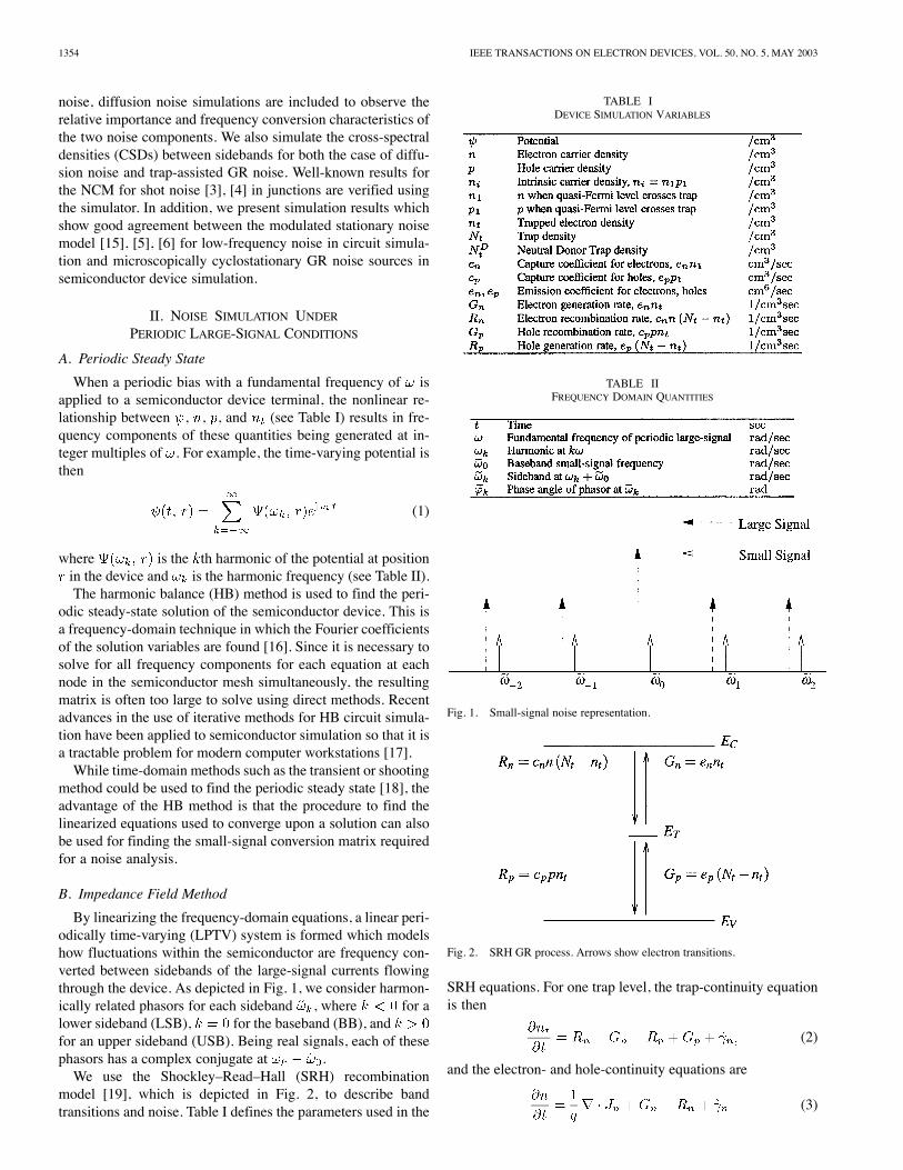
odically time-varying (LPTV) system is formed which modelshow fluctuations within the semiconductor are frequency con-verted between sidebands of the large-signal currents flowingthrough the device. As depicted in Fig. 1, we consider harmon-ically related phasors for each sideband , where for alower sideband (LSB), for the baseband (BB), andfor an upper sideband (USB). Being real signals, each of thesephasors has a complex conjugate at .We use the Shockley–Read–Hall (SRH) recombination
model [19], which is depicted in Fig. 2, to describe bandtransitions and noise. Table I defines the parameters used in the
TABLE IDEVICE SIMULATION VARIABLES
TABLE IIFREQUENCY DOMAIN QUANTITIES
Fig. 1. Small-signal noise representation.
Fig. 2. SRH GR process. Arrows show electron transitions.
SRH equations. For one trap level, the trap-continuity equationis then
(2)
and the electron- and hole-continuity equations are
(3)

SANCHEZ et al.: TWO-DIMENSIONAL SEMICONDUCTOR DEVICE SIMULATION OF TRAP-ASSISTED NOISE 1355
(4)
and Poisson’s equation is stated as
(5)
where is the density of donor-like traps, and , , andare the Langevin terms corresponding to fluctuations in the
steady-state GR transition rates in the electron-, hole-, and trap-continuity equations, respectively.By placing a source in each linearized PDE describing the
semiconductor device, it is possible to couple perturbations inthe microscopic GR rates in the semiconductor with a voltageor current response at the device terminals. For trap-assisted GRfluctuations, the cross-spectral density between a response atexternal circuit node at and node at is
(6)
where is the scalar Green’s function which cou-ples GR fluctuations for each differential volume from theelectron- ( ), hole- ( ), or trap- ( ) continuityequation at frequency to a response at circuit node at fre-quency . Using modified nodal analysis, and can also rep-resent current through a voltage source [20]. The noise sourcestrength accounts for the correlation of tran-sition-rate fluctuations between equations and at sidebandfrequencies and , respectively, and is defined in the nextsection.Diffusion noise is found using [1], [11]
(7)
where
(8)
is the vector Green’s function and is thenoise source strength tensor for velocity fluctuations.The total CSD is then given by
(9)
C. Cyclostationary Noise Analysis1) Modulated Stationary Noise Model: We use the modu-
lated stationary noise model [6] to model the instantaneous biasdependence of the microscopic noise sources. This model hasbeen used to describe the modulation of shot noise in diodes[3], [4] in circuit simulation and has been recently applied tothe modulation of microscopic noise sources in device simu-lation [11]. This model applies when the correlation time of anoise process ismuch shorter than the period of an applied large-
signal bias and is applicable to microscopic diffusion noise andGR noise phenomena. Consider a noise process given by
(10)
where is the modulating function described by
(11)
and is an instantaneous function of the solution variables andis a unit stationary noise source with
(12)
where is a random phase angle and .It can be shown that the CSD between noise phasors at side-
band frequencies and is then [3]
(13)
In order to properly account for the total noise, it is necessary toaccount for the contribution of both the self- and cross-spectralcomponents to the output response of the semiconductor devicethrough the time-varying Green’s functions as described by (6)and (7).2) GR Noise Sources: If the fundamental source of the-like fluctuations in a semiconductor can be attributed to
GR events, it is possible to apply the IFM and the modulatedstationary noise model so that low-frequency noise can besimulated under periodic large-signal conditions. The GRtransition-rate fluctuations between the conduction or valenceband and the trap level are white processes so that (13) applies.For one trap level, the time-derivative term in (2) often resultsin a Lorentzian frequency spectrum when coupled to the devicecontact. For a proper distribution in energy or position for thetraps, the low-frequency noise can produce a spectrum[21].Being a shot process, the microscopic GR noise sources have
an autocorrelation of [9]
(14)
and and are the instantaneous GR rates betweenthe conduction band ( ) or valence band ( ) and thetrap level. Using (13), the noise source strengths for use in (6)are then
(15)
(16)
(17)(18)
where
(19)

1356 IEEE TRANSACTIONS ON ELECTRON DEVICES, VOL. 50, NO. 5, MAY 2003
Fig. 3. Equivalent noise current generator.
where and are the Fourier coefficientsof the spatially dependent generation and recombination rates,respectively.3) Diffusion Noise Sources: The noise source strength
tensor used in (7) for velocity fluctuations is
(20)
where is the diffusivity and is the th harmonic ofthe carrier density. For the purposes of our investigation, we usethe Einstein relationship
(21)
to find the noise source from the low-field mobility. For 2-Dand three-dimensional (3-D) simulation it is appropriate touse a frequency dependent diffusivity tensor to account forcrystallographic direction [1] and frequency components of thediffusivity/carrier-density product to account for the electricfield dependence of the diffusivity [11]. Since our focus is the
-like low-frequency noise, no attempt was made to accountfor the diffusivity outside of equilibrium. This microscopicnoise source results in shot noise observed in diodes andthermal noise in resistors. An additional reduced shot noisecomponent may stem from GR transitions in the quasi-neutralregions and is accounted for by (14)–(19) [9].
III. NCM FOR CIRCUIT SIMULATION
A. TheoryFor dc steady-state noise analysis in circuits, an equivalent
current-noise generator is used to model the noise of thesemiconductor devices in a circuit at the small-signal frequencybeing considered. The current generator for a two-terminaljunction device is shown in Fig. 3. While our simulation resultsin Section IV are for a three-terminal device, we limit ourdiscussion to this device in order to simplify the multiportfrequency discussion.Since the noise is instantaneously dependent on bias, anNCM
is required to account for the cross correlation between the cur-rent phasors at each sideband under periodic large-signal condi-tions. If the large-signal behavior of an equivalent noise gener-ator for circuit simulation is unknown, we show in this section
Fig. 4. Network representation of correlated noise generators for a one-portdevice.
how it may be found bymodeling the fundamental noise sourcesin a semiconductor device simulator.When a device is placed in a circuit under periodic steady-
state conditions, the response is
(22)
where is a vector of correlated current phasors at the harmon-ically related sideband frequencies, is the admittance matrixformed by linearizing the nodal circuit equations, and is thevoltage response at each sideband for every node in the circuit[22]. Using modified nodal analysis [20], the current responsethrough each voltage source is also found.The resulting noise spectral density at node and frequencyis then
(23)
where is the row of corresponding to output nodeat frequency , denotes the transpose conjugate, and
is the NCM where each column is a vector of corre-lated noise components.Fig. 4 shows a network representation of how noise current
generators at each sideband frequency contribute to the totalnoise spectral density for a one-port device. A port representingsideband has a noise generator , which represents thecurrent spectral density at that sideband. The input impedanceof the semiconductor device at is represented by . Inaddition, represents the impedance of the terminationpresented to the device. A large-signal voltage source applieddirectly to the device presents a short-circuit condition to eachsideband frequency, , so that the noise generator at each fre-quency is unable to mix to other sidebands via the impedance ofthe device. A noise simulation under this condition would also

SANCHEZ et al.: TWO-DIMENSIONAL SEMICONDUCTOR DEVICE SIMULATION OF TRAP-ASSISTED NOISE 1357
result in . In addition, a cross-spec-tral density simulation between sidebands and would resultin .Using a semiconductor device simulator, (6) can be used to
find the NCM entries for low-frequency GR noise sources foruse in circuit simulation. If an equivalent current noise gener-ator has been placed between nodes and in a compact noisemodel, its NCM for low-frequency GR noise can be simulatedin a semiconductor device simulator by placing a large-signalvoltage source between these same nodes. The resulting NCMentry relating a current generator connected between nodesand at sideband frequencies and is then
(24)
In Section IV, simulation results are presented which demon-strate how this method is used to generate the NCM entries forlow-frequency cyclostationary trap-assisted GR noise sources.The methodology presented in this section is adequate for sim-ulation of an intrinsic device. In the case of an extrinsic resis-tance, the model in Fig. 3 would require the addition of a serieselement between the intrinsic device and the device terminal[23]. This method could then only be used if these parasiticsare small enough as to not interfere with the large-signal opera-tion of the device. In addition, the resistance must then be muchsmaller than the small-signal input impedance of the intrinsicdevice throughout the entire range of the applied bias.While it is not always possible to generate an analytical model
from such information, we attempt to apply known compact cy-clostationary noise models for shot noise in diodes [3] and mi-croscopically stationary low-frequency noise in linear resistors[23]–[25] to a BJT.
B. Diffusion NoiseFor a junction diode, the shot noise is instantaneously depen-
dent on bias so that the current spectral density observed at allsmall-signal frequencies is
(25)
where is the large-signal current and has units ofA /Hz. Using (13), the NCM entries which couple the noisegenerator at with the noise generator at are [4]
(26)(27)
where is the th harmonic of the large-signalcurrent flowing through the diode and and are the nodes towhich the current generator is attached (see Fig. 3). The minussign in (27) accounts for the fact that current phasors enteringnode are leaving node .
C. GR NoiseThe GR transition rates may be invariant (stationary) or
variant (cyclostationary) with respect to an applied periodicbias. Regardless of whether or not the microscopic noisesources are bias dependent, a compact model would require an
NCM. This is since harmonics of the periodic scalar Green’sfunctions could modulate bias independent GR fluctuations intocorrelated current density fluctuations at the device terminals.In the literature, -like noise and GR noise have been ob-
served in resistors and junction devices, such as bipolar junctiontransistors [26]. For GR noise the spectra is often observed as
(28)
where is the dc current flowing into the device and .The equivalent noise generator for low-frequency noise in a BJTmodel is often placed between the base and emitter junction[26] and dependent on the base current. It is not known howthese noise sources vary under large-signal bias conditions whenthe microscopic noise sources in the internal device are biasdependent.For a resistor, low-frequency GR fluctuations may be viewed
as bias independent (stationary) resistivity fluctuations whichare modulated by the large-signal currents flowing through thedevice so that correlated current components exist at each side-band [12]. The current spectral density is then quadratically de-pendent on the current flowing through the device. In this sec-tion, we develop this model and in Section IV we investigate ifthis model can be more generally applied to noise in a BJT de-vice.If we consider these resistivity fluctuations as being sta-
tionary, the modulated stationary model applies, except thatthe stationary noise source is lowpass filtered. Equation (12)becomes
(29)
where is function of frequency. The CSD between side-bands is then
(30)
where
(31)
The NCM entries for a stationary low-frequency noise sourcewith a quadratic current-dependence are then
(32)
where . For a single trap
(33)
where and are constants. For flicker noise
(34)

1358 IEEE TRANSACTIONS ON ELECTRON DEVICES, VOL. 50, NO. 5, MAY 2003
Fig. 5. BJT doping profile. Greyscale units are . 0.15- memitter contact is located at the upper-left corner, the collector contact is alongthe bottom, and the 0.15- m base contact is located at the upper-right-hand side.
For RF and microwave applications, for andso that
(35)
In [25], it is demonstrated that (35) is applicable for a non-linear resistor in which band-to-band GR transitions occur. Inthis approach, the device is a homogeneously doped resistor sothat the microscopic noise sources do not vary. When the mi-croscopic noise sources are functions of the instantaneous bias,it is not known if it is possible to use an expression like (32) todescribe the equivalent input current noise generator. In the liter-ature, the modulated stationary noise model has been applied ingeneral to low-frequency noise [5], [6], although it is not knownif it is appropriate for all types of low-frequency noise.Commercial circuit simulators, such as Agilent Advanced de-
sign system (ADS), treat low-frequency noise as being depen-dent on the dc component of the current flowing through the de-vice [27]. However, such a model does not predict the presenceof low-frequency noise around the USBs and LSBs under acshort-circuited conditions, as was observed for a linear resistorand a - junction [12]. In the next section, we present sim-ulation results which compare (35) with a semiconductor noisesimulation under periodic large-signal conditions.
IV. SIMULATION RESULTS
A. Shot NoiseA silicon / / BJT was simulated in FLOODS with the
dimensions and doping profile shown in Fig. 5. The 0.15- memitter contact is located at the upper-left corner and was mod-eled with a surface recombination velocity of cm/s.The collector contact is along the bottom and the 0.15- m basecontact is located at the upper-right-hand side. The device hadan emitter depth of 70 nm and a base width of 70 nm. TheKlaassen mobility model [28] at 300 K was used for all sim-ulations.The diffusion noise for increasing dc bias on the base was
simulated for V. The simulation results for base
Fig. 6. Base and collector shot noise of the BJT.
Fig. 7. Test circuit for the harmonic balance and noise simulation.
Fig. 8. Cross-spectral current densities for base shot noise for increasing acbias. Symbols denote device simulation of (7) and dashed lines are calculatedfrom (26).
and collector shot noise versus are shown in Fig. 6. Theseresults agreed well with the shot noise expressions of
and .For the HB simulation, the circuit shown in Fig. 7 was used
with V, V and V.A noise simulation was performed for each sideband for in-creasing AC bias. The steady-state simulation was performedwith five frequencies, including dc. This results in a conversionmatrix relating nine sideband frequencies. Fig. 8 shows thecross-spectral current densities for the base current betweenthe first USB and other sidebands denoted by , where

SANCHEZ et al.: TWO-DIMENSIONAL SEMICONDUCTOR DEVICE SIMULATION OF TRAP-ASSISTED NOISE 1359
Fig. 9. Cross-spectral current densities for collector shot noise. Dotted linesuse the model described by (26).
Fig. 10. Real part of the correlation between the base and collector shot noiseat the BB for increasing ac bias. Imaginary part was negligible.
denotes the sideband at frequency . Excellent agreementwas found between the simulated data and the NCM entry forshot noise given by (26).Collector shot noise for increasing ac bias is shown in Fig. 9.
The simulation begins to deviate from (26) for higher ac bias.This corresponds to the deviation between the simulation andanalytical shot-noise model for the dc results shown in Fig. 6and is attributed to high-level injection effects.Fig. 10 shows the correlation between the base and collector
shot noise at which was calculated as
(36)
This indicates that the equivalent current noise generators forthe base and collector can be treated independently, even underlarge-signal ac conditions. Similar results were found when thecross correlation between the base and collector noise was eval-uated at each sideband frequency.
B. GR NoiseThe same BJT device was simulated with an electron cap-
ture coefficient of cm /s and an energy level ofeV. Similar trap parameters were reported for
Fig. 11. Relative noise contributions of GR noise to the base current noise.Greyscale units are .
Fig. 12. Relative noise contributions of GR noise to the collector current noise.Greyscale units are .
a polysilicon-emitter BJT in the literature [29] with the traps as-cribed to the emitter region at or near the polysilicon–monosil-icon interface. A constant trap density of /cm wassimulated for the device in order to find the relative contribu-tions of the device regions. The distributed contributions to theshort-circuit base current noise and collector current noise for
V are shown in Figs. 11 and 12, respectively. Forthis trap energy level, the dominant noise contribution to thebase noise is between the base and the emitter near the surface.A possible source of traps for this region would be the interfacebetween the silicon and the oxide spacer between the base andemitter contacts [26].Noise was then simulated for donor-like traps at a depth of
0 m (see Fig. 5) between the base and emitter contact with/cm .1 Figs. 13 and 14 show both the GR and
shot noise versus current at the base and collector, respectively.Fig. 15 shows the electron quasi-Fermi level forV at the surface of the device. It shows that near this bias con-dition, the electron quasi-Fermi-level is close to the trap-level1The surface density is a volume density distributed over 1.5 nm at the surface.

1360 IEEE TRANSACTIONS ON ELECTRON DEVICES, VOL. 50, NO. 5, MAY 2003
Fig. 13. Shot andGR current noise at the base versus for dc bias conditions.Symbols denote device simulation and the dotted line is calculated from
.
Fig. 14. Shot and GR current noise at the collector versus .
Fig. 15. Electron quasi-Fermi level and the trap energy level at thesurface for V. Active traps for noise are where and intersect.
over the entire interface between the contacts. At lower biases aquadratic dependence of noise spectral density on dc current isobserved and is attributed to trapping noise in the space chargeregion of the device. As bias is increased, the space chargeregion narrows, and the position where the quasi-Fermi levelfor electrons crosses the trap level moves into the quasi-neutralregion and the quadratic current dependence is lost. At much
Fig. 16. Upper sideband and baseband noise spectra of the base terminalcurrent for 2 large-signal ac bias values. Low-frequency plateau is due to thetrap-assisted GR noise. High-frequency plateau is the diffusion noise floor.
Fig. 17. Device simulation of upper sideband GR noise plateaus using(6) versus large-signal ac bias compared with circuit simulation using (35).Simulations were performed to the base terminal current. Symbols denotedevice simulation and dotted lines denote circuit simulation.
higher biases, a high-level injection of electrons causes the lo-cation of this crossing to move toward the base contact so thearea of active traps is reduced and the noise rolls off.Using the same bias conditions as in Section IV-A the noise
in the base terminal current was simulated versus frequency forincreasing ac bias. In Fig. 16, the USB andBB spectra are shownfor an ac bias of 0, 50, and 100 mV. The low-frequency plateauis the GR noise component while the high-frequency plateau isthe diffusion noise floor. It is apparent that the corner frequency
Hz is invariant to the ac bias. The USB plateaus versusac bias are shown in Fig. 17. The BB level was fit to the NCMmodel of (35) and (33) with /Hz and using thedc component of the base current for increasing ac bias. Usingthis value of and the harmonics of the base current, the resistorGR noise model was applied to each of the sidebands in Fig. 17and good agreement was found between device simulation of(6) and the circuit model. Fig. 18 shows the base current CSDbetween the first USB and several other sidebands. Again, goodagreement was found between device simulation and the circuitmodel.Fig. 19 shows the simulated GR spectrum at the BB and USB
at 50 mV ac bias. In addition, the magnitude of their CSD is

SANCHEZ et al.: TWO-DIMENSIONAL SEMICONDUCTOR DEVICE SIMULATION OF TRAP-ASSISTED NOISE 1361
Fig. 18. Device simulation of the cross-spectral density of the low-frequencyGR plateaus to the first USB for increasing ac bias. Simulations were performedto the base terminal current. Symbols denote device simulation and dotted linesdenote circuit simulation.
Fig. 19. Device simulation of theGR noise spectrum at the baseband and uppersideband and their cross-spectral density. Simulated NCM using (33) is shownwith dotted lines.
shown. Using the value of and in (33), goodagreement was found between the microscopic GR model andthe equivalent NCM model.The GR noise shown in the simulations had a near quadratic
dependence on current. The good agreement for the stationaryfluctuation model derived as (32) and the simulations was sur-prising since the the noise producing trapped carrier densitywas a function of instantaneous bias and the current dependenceshown in Fig. 13 did not have an exact exponent of 2. This vari-ation is attributed to the spatial position of active traps versusbias. In [11], the authors model low-frequency GR and flickernoise as being microscopically stationary and consider equiva-lent current density noise sources. They speculate that since thebias is varying at a frequency much larger than the corner fre-quency of the noise, that the trap is not able to respond.In Fig. 16, the low-frequency GR noise rapidly increases
about two orders of magnitude over the diffusion noise floor asthe ac bias increases. This demonstrates that the effects of GRnoise which is not considered significant in dc measurementor simulation may become important in mixer circuit or phasenoise as the ac bias is increased. This effect depends on thecircuit boundary conditions that the device is presented with.
In the literature, (32) is typically used for cyclostationarynoise analysis in noise simulators without experimental or theo-retical verification. The simulations presented in this paper pro-vide evidence that such a model is applicable to low-frequencynoise due to trap-assisted GR noise. The trap-assisted GRmodelcould not be applied to the case of cyclostationary effects inMOSFET’s, where the trapping occurs into the oxide [30]. It is,therefore, not known if this model could always be applied whenthe spectral density of the noise has a quadratic dependence oncurrent such as for mobility fluctuations [21] or tunneling fluc-tuations through the mono/polysilicon interface of BJTs [26].The simulation results in this section do provide evidence thatthe cyclostationary noise model can be applied to BJTs whentraps are near the Si–SiO interface at the device surface.
V. CONCLUSION
This paper presents the 2-D semiconductor device simula-tions of diffusion and GR noise under periodic large-signal con-ditions. In addition, our work indicates that a semiconductor de-vice simulator can be used to justify and develop circuit noisemodeling approaches. We also show that low-frequency noisedue to trap-assisted GR fluctuations can be modeled using themodulated stationary noise model for the purposes of circuitsimulation.
ACKNOWLEDGMENT
The authors would like to thank the reviewers for their carefulreading of this manuscript and helpful suggestions. The authorswould also like to thank F.-C. Hou and D. Martin for their par-ticipation in the development of noise simulation capabilities inFLOODS.
REFERENCES[1] F. Bonani, S. D. Donati, G. Ghione, and M. Pirola, “A TCAD approach
to the physics-based modeling of frequency conversion and noise insemiconductor devices under large-signal forced operation,” IEEETrans. Electron Devices, vol. 48, pp. 966–977, May 2001.
[2] K. Mayaram, D. C. Lee, S. Moinian, D. A. Rich, and J. Roychowd-hury, “Computer-aided circuit analysis tools for RFIC simulation: Al-gorithms, features, and limitations,” IEEE Trans. Circ. Syst. II, vol. 47,pp. 274–286, Apr. 2000.
[3] C. Dragone, “Analysis of thermal and shot noise in pumped resistivediodes,” Bell Syst. Tech. J., vol. 47, pp. 1883–1902, 1968.
[4] D. N. Held and A. R. Kerr, “Conversion loss and noise of microwaveand millimeter-wave mixers: Part 1—Theory,” IEEE Trans. MicrowaveTheory Tech., vol. MTT-26, pp. 49–54, Feb. 1978.
[5] A. Demir and A. Sangiovanni-Vincentelli, Analysis and Simulation ofNoise in Nonlinear Electronic Circuits and Systems. Boston, MA:Kluwer, 1998.
[6] J. S. Roychowdhury, D. Long, and P. Feldmann, “Cyclostationary noiseanalysis of large RF circuits with multitone excitations,” IEEE J. Solid-State Circuits, vol. 33, pp. 324–336, Mar. 1998.
[7] A. van der Ziel, “Unified presentation of noise in electronic devices:Fundamental noise sources,” Proc. IEEE, vol. 76, pp. 233–258,Mar. 1988.
[8] W. Shockley, J. A. Copeland, and R. P. James, “The impedancefield method of noise calculation in active semiconductor devices,”in Quantum Theory of Atoms, Molecules, and the Solid-State, P.-O.Lowdin, Ed. New York: Academic, 1966, pp. 537–563.
[9] K. M. van Vliet, “Noise and admittance of the generation-recombinationcurrent involving SRH centers in the space-charge region of junctiondevices,” IEEE Trans. Electron Devices, vol. ED-23, pp. 1236–1246,Nov. 1976.

1362 IEEE TRANSACTIONS ON ELECTRON DEVICES, VOL. 50, NO. 5, MAY 2003
[10] F. Bonani, G. Ghione, M. R. Pinto, and R. K. Smith, “An efficientapproach to noise analysis through multidimensional physics-basedmodels,” IEEE Trans. Electron Devices, vol. 45, pp. 261–269, Jan.1998.
[11] A. Cappy, F. Danneville, G. Dambrine, and B. Tamen, “Noise analysisin devices under nonlinear operation,” Solid-State Electron., vol. 43, pp.21–26, 1999.
[12] J. E. Sanchez, G. Bosman, and M. E. Law, “Device simulation of gen-eration-recombination noise under periodic large-signal conditions,” inIEDM Tech. Dig., 2001, pp. 477–480.
[13] M. Liang and M. E. Law, “Influence of lattice self-heating and hot-car-rier transport on device performance,” IEEE Trans. Electron Devices,vol. 41, pp. 2391–2398, Dec. 1994.
[14] , “An object-oriented approach to device simulation—FLOODS,”IEEE Trans. Computer-Aided Design, vol. 13, pp. 1235–1240, Oct.1994.
[15] B. A. Kramer, “Frequency conversion analysis of noise in heterojunc-tion bipolar transistor oscillators including periodically modulated noisesources,” Ph.D. dissertation, Iowa State Univ., Ames, IA, 1993.
[16] K. S. Kundert, J. K.White, andA. Sangiovanni-Vincentelli, Steady-StateMethods for Simulating Analog and Microwave Circuits. Norwell,MA: Kluwer, 1990.
[17] B. Troyanovsky, Z. Yu, and R. W. Dutton, “Physics-based simulation ofnonlinear distortion in semiconductor devices using the harmonic bal-ance method,” Comput. Methods Appl. Mech. Eng., vol. 181, no. 4, pp.467–482, Jan. 2000.
[18] Y. Hu and K. Mayaram, “Periodic steady-state analysis for coupled de-vice and circuit simulation,” in Proc. IEEE SISPAD, 2000, pp. 90–93.
[19] S. S. Li, Semiconductor Physical Electronics. New York: Plenum,1993.
[20] W. J. McCalla, Fundamentals of Computer-Aided Simulation. Boston,MA: Kluwer, 1987.
[21] F. N. Hooge, “ noise sources,” IEEE Trans. Electron Devices, vol.41, pp. 1926–1935, Nov. 1994.
[22] S. A.Maas,MicrowaveMixers, 2nd ed. Norwood,MA: Artech House,1993.
[23] A. van der Ziel, Noise in Solid State Devices and Circuits. New York:Wiley, 1986.
[24] J. H. J. Lorteije and A. M. H. Hoppenbrouwers, “Amplitude modulationby noise in resistors results in noise,” Philips Res. Rep., vol.26, no. 1, pp. 29–39, 1971.
[25] F. Bonani, S. D. Guerrieri, and G. Ghione, “Noise source modeling forcyclostationary noise analysis in large-signal device operation,” IEEETrans. Electron Devices, vol. 49, pp. 1640–1647, Sept. 2002.
[26] M. J. Deen, J. Ilowski, and P. Yang, “Low frequency noise in polysilicon-emitter bipolar junction transistors,” J. Appl. Phys., vol. 77, no. 12, pp.6278–6288, June 1995.
[27] Agilent Advanced Design System. Palo Alto, CA: Agilent Technolo-gies, 2000.
[28] D. B. M. Klaassen, “A unified mobility model for device simulation—I.Model equations and concentration dependence,” Solid-State Electron.,vol. 35, no. 7, pp. 953–959, June 1992.
[29] M. Sandén, O. Marinov, M. Deen, and M. Ostling, “A newmodel for thelow-frequency noise and the noise level variation in polysilicon emitterBJTs,” IEEE Trans. Electron Devices, vol. 49, pp. 514–520, Mar. 2002.
[30] E. A. M. Klumperink, S. L. J. Gierkink, A. P. van der Wel, and B. Nauta,“Reducing MOSFET noise and power consumption by switchedbiasing,” IEEE J. Solid-State Circuits, pp. 994–1001, 2000.
Juan E. Sanchez (S’92–M’03) received the B.S.E.E.degree in 1995 from the University of South Florida,Tampa, and the M.S. and Ph.D. degrees from theUniversity of Florida, Gainesville, in 1997 and2002, respectively, both in electrical and computerengineering.His graduate research concerned measurement and
semiconductor device simulation of noise under pe-riodic large-signal conditions. He is now with Syn-opsys, Inc., Mountain View, CA, where he is a TCADR&D Engineer. His research interests include RF-re-
lated issues in semiconductor device simulation.Dr. Sanchez is a member of the IEEE Electron Device Society.
Gijs Bosman (SM’01) received the B.S., M.S., andPh.D. degrees in physics from the University ofUtrecht, Utrecht, The Netherlands in 1971, 1976,and 1981, respectively.In 1981, he joined the Department of Electrical
and Computer Engineering, University of Florida,Gainesville, where he is currently a Professor andAssociate Chair. His research interests include theelectrical noise and charge transport propertiesof semiconductor devices and circuits. He haspublished more than 100 refereed journal and
conference papers on these topics. He is an Editor of Fluctuations and NoiseLetters.Dr. Bosman was the General Chair and host of the 16th International Confer-
ence on Noise in Physical Systems and Fluctuations, held in Gainesville,FL, in the fall of 2001. He serves on the International Advisory Committee onNoise and Fluctuations. He is a Member of the American and Dutch Physicalsocieties. In addition to the College of Engineering Teacher of the Year Awardfor 1998–1999, he has received several university and departmental awards forteaching and research.
Mark E. Law (F’98) received the B.S.Cpr.E. degreefrom Iowa State University, Ames, in 1982, and theM.S.E.E. degree and the Ph.D. degree from StanfordUniversity, Stanford, CA, in 1982 and 1988, respec-tively.He is a Professor of electrical and computer
engineering at the University of Florida (UF),Gainesville. He worked at Hewlett Packard from1982 to 1985 and joined the faculty at Florida in1988. He is currently Co-Director of the Softwareand Analysis of Advanced Materials Processing
(SWAMP) center at UF. His current research interests include integrated circuitprocess modeling and characterization. As a graduate student, he coauthoredSUPREM-IV, and his research group at (UF) developed the Florida ObjectOriented Process Simulator (FLOOPS). His research has focused on themodeling of point defects and dopant diffusion in silicon. He has written over100 papers in the area of process and device modeling.Dr. Law was named a National Science Foundation Presidential Faculty
Fellow in 1992, Outstanding Young Alumni of Iowa State in 1994, College ofEngineering Teacher of the Year in 1996–1997, and a UF Research Fellow in1998. The FLOOPS development effort won the 1993 Semiconductor ResearchCorporation (SRC) Technical Excellence Award. He was Editor-in-Chief ofthe IEEE JOURNAL ON TECHNOLOGY COMPUTER-AIDED DESIGN from 1992 to2002 and has served as an Editor of IEEE TRANSACTIONS ON SEMICONDUCTORMANUFACTURING. He chaired the 1997 Simulation of Semiconductor Processand Devices Meeting, the 1999 Silicon Front-End Processing Symposium ofthe Materials Research Society, and chaired the 2000 International ElectronDevices Meeting. He has served on technical committees for several otherconferences.