Two-dimensional numerical modeling of lightly doped nano-scale double-gate MOSFET
9
Two-dimensional numerical modeling of lightly doped nano-scale double-gate MOSFET Deepanjan Datta, A. Ananda Prasad Sarab, S. Dasgupta * Department of Electronics Engineering, Indian School of Mines, Jharkhand, Dhanbad 826004, India Received 5 May 2005; received in revised form 24 July 2005; accepted 27 July 2005 Available online 9 September 2005 Abstract A two-dimensional numerical solution of electrostatic potential and electric field profiles are presented for lightly doped nano-scale Double-Gate Metal-Oxide-Semiconductor-Field-Effect-Transistor (DG-MOSFET). We have developed quasi-static (QS) model for evaluating bulk and inversion charges based on symmetric linearization model. We have also shown the non-quasi-static (NQS) effect on the charge due to a time varying gate voltage. It is seen that various symmetries of DG-MOSFET characteristics with respect to source/drain interchange is maintained in quasi-static as well as non-quasi-static version of the symmetrically linearized model. The variation of the threshold voltage with the varying width of the device is evaluated and presented. The results have been compared and contrasted with reported analytical model for QS condition for the purpose of verification of the model. The variation of threshold voltage along the width of the device is also predicted. This numerical model can be extended to analyze the transport phenomenon in sub 30 nm channel length DG-MOSFETs. q 2005 Elsevier Ltd. All rights reserved. Keywords: Nano-scale modeling; Double gate MOSFET; Quasi-static charge; Non-quasi-static charge; QM modeling 1. Introduction As CMOS technology progresses, device dimensions have been scaled to nano-scale regime [1]. Therefore, in future transistors may operate near their ballistic limit rendering it is important to understand the ballistic device physics. An accurate modeling of nano-scale DG-MOSFET is essential using 2D simulator to accomplish the perform- ance analyses because of expected 2D Short Channel Effect (SCE). In low drain bias 1D electrostatics is sufficient to explain the characteristics of DG-MOSFET. But, at high drain bias, important 2D electrostatic effects like drain induced barrier lowering (DIBL) and threshold voltage roll- off can be explained using 2D modeling of nano-scale DG-MOSFET. As CMOS scaling is approaching the limit imposed by gate oxide tunneling, scaling down DG MOSFET is becoming a subject of intense VLSI research [2]. The advantages for DG MOSFET are ideal 60 mV/Dec sub-threshold slope [3], scaling by silicon film thickness without high doping, etc. Aggressive scaling of oxide layer thickness is required to provide substantial current drive to suppress SCEs such as Drain Induced Barrier Lowering (DIBL). To predict qualitatively the short channel threshold-voltage (V t ) roll- off and DIBL, full numerical potential model is described which includes both symmetric and asymmetric short channel DG-MOSFET models. These numerical results are essential for predicting the transport phenomena in short channel devices. Chen et al. [4] developed a unique non- equilibrium Green’s function approach (S.E.M.C.) for determining the characteristics of DG-MOSFET, which provides a physically rigorous approach to quantum approach and real scattering process. In another paper [5], Winstead and Ravaioli, modeled a 25 nm MOS capacitor which includes the non-equilibrium ballistic transport with quantum correction. Villanueva and Gamiz [6] have investigated the role of centroid inversion layer in DG-MOSFET. Here, the magnitude of the inversion layer centroid has been analyzed in volume-inversion transistors, where the minority carrier distribution has been found to be Microelectronics Journal 37 (2006) 537–545 www.elsevier.com/locate/mejo 0026-2692/$ - see front matter q 2005 Elsevier Ltd. All rights reserved. doi:10.1016/j.mejo.2005.07.009 * Corresponding author. Tel.: C91 326 220 6866; fax: C91 326 221 0028 E-mail address: [email protected] (S. Dasgupta).
-
Upload
deepanjan-datta -
Category
Documents
-
view
213 -
download
0
Transcript of Two-dimensional numerical modeling of lightly doped nano-scale double-gate MOSFET

Two-dimensional numerical modeling of lightly doped nano-scale
double-gate MOSFET
Deepanjan Datta, A. Ananda Prasad Sarab, S. Dasgupta*
Department of Electronics Engineering, Indian School of Mines, Jharkhand, Dhanbad 826004, India
Received 5 May 2005; received in revised form 24 July 2005; accepted 27 July 2005
Available online 9 September 2005
Abstract
A two-dimensional numerical solution of electrostatic potential and electric field profiles are presented for lightly doped nano-scale
Double-Gate Metal-Oxide-Semiconductor-Field-Effect-Transistor (DG-MOSFET). We have developed quasi-static (QS) model for
evaluating bulk and inversion charges based on symmetric linearization model. We have also shown the non-quasi-static (NQS) effect on the
charge due to a time varying gate voltage. It is seen that various symmetries of DG-MOSFET characteristics with respect to source/drain
interchange is maintained in quasi-static as well as non-quasi-static version of the symmetrically linearized model. The variation of the
threshold voltage with the varying width of the device is evaluated and presented. The results have been compared and contrasted with
reported analytical model for QS condition for the purpose of verification of the model. The variation of threshold voltage along the width of
the device is also predicted. This numerical model can be extended to analyze the transport phenomenon in sub 30 nm channel length
DG-MOSFETs.
q 2005 Elsevier Ltd. All rights reserved.
Keywords: Nano-scale modeling; Double gate MOSFET; Quasi-static charge; Non-quasi-static charge; QM modeling
1. Introduction
As CMOS technology progresses, device dimensions
have been scaled to nano-scale regime [1]. Therefore, in
future transistors may operate near their ballistic limit
rendering it is important to understand the ballistic device
physics. An accurate modeling of nano-scale DG-MOSFET
is essential using 2D simulator to accomplish the perform-
ance analyses because of expected 2D Short Channel Effect
(SCE). In low drain bias 1D electrostatics is sufficient to
explain the characteristics of DG-MOSFET. But, at high
drain bias, important 2D electrostatic effects like drain
induced barrier lowering (DIBL) and threshold voltage roll-
off can be explained using 2D modeling of nano-scale
DG-MOSFET. As CMOS scaling is approaching the limit
imposed by gate oxide tunneling, scaling downDGMOSFET
is becoming a subject of intense VLSI research [2].
0026-2692/$ - see front matter q 2005 Elsevier Ltd. All rights reserved.
doi:10.1016/j.mejo.2005.07.009
* Corresponding author. Tel.: C91 326 220 6866; fax: C91 326 221
0028
E-mail address: [email protected] (S. Dasgupta).
The advantages for DG MOSFET are ideal 60 mV/Dec
sub-threshold slope [3], scaling by silicon film thickness
without high doping, etc.
Aggressive scaling of oxide layer thickness is required to
provide substantial current drive to suppress SCEs such as
Drain Induced Barrier Lowering (DIBL). To predict
qualitatively the short channel threshold-voltage (Vt) roll-
off and DIBL, full numerical potential model is described
which includes both symmetric and asymmetric short
channel DG-MOSFET models. These numerical results
are essential for predicting the transport phenomena in short
channel devices. Chen et al. [4] developed a unique non-
equilibrium Green’s function approach (S.E.M.C.) for
determining the characteristics of DG-MOSFET, which
provides a physically rigorous approach to quantum
approach and real scattering process. In another paper [5],
Winstead and Ravaioli, modeled a 25 nm MOS capacitor
which includes the non-equilibrium ballistic transport with
quantum correction. Villanueva and Gamiz [6] have
investigated the role of centroid inversion layer in
DG-MOSFET. Here, the magnitude of the inversion layer
centroid has been analyzed in volume-inversion transistors,
where the minority carrier distribution has been found to be
Microelectronics Journal 37 (2006) 537–545
www.elsevier.com/locate/mejo

Fig. 1. Schematic of the Double Gate MOSFET under study.
D. Datta et al. / Microelectronics Journal 37 (2006) 537–545538
closer to the interfaces in volume inversion transistors and
therefore, some of the advantages assumed in the device
have been grounded. Ren and Lundstrom [7] have derived
the numerical simulation technique from a Schrodinger–
Poisson tool applied to DG MOSFET where essential
physics governing the transport phenomena is presented to
give the insight concerning the near-ideal features of
DG-MOSFET. A compact, physics based short channel
models of sub threshold swing and threshold voltage model
[8] is presented for undoped symmetric DG-MOSFETs,
which includes quantum-mechanical and fringe-induced
barrier lowering effects. Baccarani et al. [9] investigated the
electrical properties of the DG MOSFET, which turn out to
be very promising for device miniaturization below 0.1 mm.
A compact model which accounts for charge quantization
within the channel, Fermi statistics, and non-static effects in
the transport model was worked out. Liu and Hosokawa [10]
investigated in a fabrication process of vertical gate DG
MOSFET using ion-bombardment-retarded etching. The
fabricated vertical DG-MOSFETs clearly exhibit the unique
advantage of DG MOSFETs, i.e. high improvement of
short-channel effect immunity by reducing the channel
thickness. An analytical expression explicitly relating the
potential and the electric field at the oxide-semiconductor
interface of a symmetrical double-gate oxide-intrinsic
semiconductor-oxide was derived by Wang et al. [11].
In this paper, the ‘turn-on’ behavior of the system was
studied and an ‘extrapolated’ threshold voltage was
uniquely defined.
In steady path of shrinking the device geometry, many
compact models for the device are proposed. However,
these models have severe drawbacks during their develop-
ment. Models like SPICE level 1 and level 2 are highly
empirical and have constrained discontinuities in their
current and capacitance characteristics. These models did
not incorporate the physics of short channel effect correctly.
Other models like MISNAN model, BNR and the Siemens
model developed by Miura-Mattausch [12] do not have
these continuities under certain limited conditions, but
display unrealistic conductance behavior at the linear/
saturation transition boundary on the output (Id–Vd)
characteristics [13]. The common problems with models
like BSIM3v3 and EKV models are that they commonly
took source a reference point due to which the expressions
containing potential, terminal charges, and transconduc-
tance lost the essential symmetry along the channel.
In this paper, we have developed a quasi-static and non-
quasi-static profile of the bulk and inversion charges of
symmetrical as well as asymmetrical DG MOSFET with
low doping levels. This paper solved the complete boundary
value to obtain numerical solution of 2D potential and
electric field profile for symmetric and asymmetric
DG-MOSFETs. For the first time, the charge profile is
developed taking into account the symmetricity with respect
to source/drain interchange in the case of DG-MOSFETs.
The bulk and inversion charge densities in both QS and
NQS profile have shown the expected symmetry at zero
drain bias. The potential and electric field profile for the
whole active area of the device has been evaluated and
presented. We have also investigated the transient phenom-
ena in terms of current flow, where gate voltage varies with
time in gaussian manner. The results obtained on the basis
of a model have been compared and contrasted with respect
to reported analytical results.
2. Numerical modeling
A 2D numerical modeling scheme has been applied to the
DG-MOSFET. Fig. 1 shows the schematic diagram of a
lightly-doped DG-MOSFET under study. The origin has
been chosen to be the centre of the Si substrate at the
source–substrate boundary as shown in Fig. 1.
For lightly doped DG MOSFETs, both the fixed and
mobile charge densities are almost negligible. In both the
insulator and silicon regions, Poisson’s equation becomes
d2J
dx2C
d2J
dy2Z
q
3Siexp
qJðx; yÞ
kT
� �(1)
If we assume the source and drain junctions are abrupt,
the boundary conditions can be written as
Jð0; yÞZVbi; KtSi2!y!
tSi2
(2)
JðL; yÞZVbi CVds; KtSi2!y!
tSi2
(3)
J x;KtSi2Ktox
� �ZVgsKDF1; 0!x!L (4)
J x;W
2C tox
� �ZVgsKDF2; 0!x!L (5)

D. Datta et al. / Microelectronics Journal 37 (2006) 537–545 539
Here, Vbi is the built-in-voltage, Vds is the applied drain
voltage, tox is the oxide layer thickness and xSi is the
permittivity of the Si layer. K is the Boltzmann coefficient
and T is the room temperature (TZ300 K). Here, L is
the channel length and tSi is the thickness of the device. The
same voltage Vgs is assumed to be applied to both the
gates. DF1 and DF2 are the work function differences
between the gate electrode 1,2 and the intrinsic silicon.
Hence, DF1Z0 for mid gap work function gate in case of
symmetric DG-MOSFET. The electrostatic potential is
defined as the intrinsic potential at point (x,y) with respect to
the Fermi potential of nC source (at the conduction band
edge).
Results show that in the insulator regions, between
source/drain and gates, the potential is given as linear
function of y, when tox/tSi!1 [14]. The potential in the
insulator gap regions are obtained by suitable interpolation
and can be expressed as:
Jð0; yÞZVbi
yC tSi2C tox
� �tox
KðVgsKDF1Þ yC tSi
2
� �tox
;
KtoxKtSi2!y!K
tSi2
(6a)
JðL; yÞZ ðVbiCVdsÞyC tSi
2C tox
� �tox
KðVgsKDF1Þ yC tSi
2
� �tox
;
KtoxKtiSi2!y!K
tSi2
(6b)
Jð0; yÞZKVbi
yKtSi2Ktox
� �tox
CðVgsKDF2Þ yKtSi
2
� �tox
;
tSi2!y!
tSi2C tox
(6c)
JðL;yÞZKðVbiCVdsÞyKtSii
2Ktox
� �tox
CðVgsKDF2Þ yKtSi
2
� �tox
;
tSi2!y!
tSi2Ctox
(6d)
In a lightly doped (or, practically undoped body)
DG-MOSFET we generally neglect hole concentration.
We have also taken aluminum (Al) as the gate metal, so
work functions of the both the gates are taken as (DF1ZDF2Z) 0.2 V for symmetric DG-MOSFETs.
A 2D numerical solution to the Poisson equation is
composed of Nx!NY potential values at each lattice node.
To attain Nx!NY unknowns, we have taken the finite
difference method and a uniform grid is superimposed on
the geometry of the channel with mesh spacing of hZ1.6!10K10 m and kZ1.6!10K10 mm along x and y-directions,
respectively. This means that at any point on the grid, using
classical discretization formula we can write
Ji;j Z1
2½JiK1;j CJiC1;j C ðh2=k2ÞðJi;jK1 CJi;jC1Þ�
!h2k2
h2 Ck2K
qh2
3Siexp
qJi;j
kT
� �(7)
where Ji,j and JiG1,jG1 are the surface potential points in
the channel. We can formulate two continuity equations at
two Si–SiO2 interfaces as:
dJ
dyyZtSi=2
ZKxSi
xOxtOxðJðx; tSi=2ÞKVgs CVfb1Þ
���� (8a)
dJ
dyyZKðtSi=2Þ
ZxSi
xOxtOxðJðx;KtSi=2ÞKVgs CVfb2Þ
���� (8b)
Here, permittivity of the oxide layer is taken as xOx. Vfb1
and Vfb2 are the flat-band voltages of the two gate sides. The
potential values in the Si layer is obtained for the solution of
Poisson’s equation under specified boundary conditions by
finite difference technique and subsequently utilized for
computing partial derivatives of J(x, y) with respect to y
and x to obtain transverse and longitudinal electric field,
respectively.
3. Quasi-static charge model for DG-MOSFET
The charge model allows one to explain the closed form
expressions for both the drain current and the terminal
charges as shown by Brews [15] and Ward et al. [16]. The
formulation by Ward et al. is however more involved than is
desirable in compact MOSFET models. Based on the
potential profile of symmetric DG-MOSFETS, we have
developed a linearized model for both the bulk charge and
the inversion charges, considering the requirements of
‘Gummel Symmetry’.
Defining normalized inversion charge density qi as, qiZQi/Cox; drain current can be expressed as
Ids ZKWCoxVqi CWCoxD dqi=dx (9)
where Qi is the inversion charge density and Cox is the
capacitance of the oxide layer. D is the diffusion co-efficient
in the steady-state drift-diffusion equation verifying the
continuity of the drain current. For the carrier velocity
expression, it is important to note that, it is symmetric with
respect to zero fields point and are continuous for all fields
within the depletion region of the device. We can take
carrier velocity as [14]:
vZmðEÞdJ
dx
� �= 1C
mðEÞ
vsat
dJ
dx
� �2� 1=2
(10)
vSAT is taken as 105 m/s [14] and m(E) is the transverse
direction dependent electric field which can be written as
[17]

D. Datta et al. / Microelectronics Journal 37 (2006) 537–545540
1
mðEÞZ
1
mc
C1
mph
C1
msr
(11)
where mc, mph and msr are coulomb scattering limited
mobility, phonon scattering limited mobility and surface
roughness scattering limited mobility, respectively.
(i) Coulomb-scattering limited mobility. Due to the
presence of fixed oxide charge, interface trapped charges
and the ionised impurities the carriers in the channel get
scattered due to coulombic perturbation, as a result the
mobility of the carriers in the surface channel decreases.
The coulomb scattering limited mobility can be modelled
as [17]
mc Z aK11 T (12)
where a1 is an extractable parameter and T is the absolute
temperature.
(ii) Phonon-scattering limited mobility. The phonon
scattering limited mobility can be modelled as [17]
mph Z aK12 TKnE
K1=geff (13)
where g and n are empirical constant. a2 is another
extractable parameter [17]. Here, Eeff is
Eeff Zq 1
2Ns CNdepl
� �3Si
(14)
Ns is the inversion layer carrier density, Ndepl is the
depletion region carrier density.
(iii) Surface roughness scattering limited mobility. This
is due to the deviation of the surface from an ideal plane.
The surface roughness scattering is independent of
temperature and is dominant at high electric fields. The
surface roughness scattering limited-mobility can be written
as [17]
msr Z aK13 EK2
eff (15)
where a3 is an extractable parameter.
From the MOS physics, normalized inversion charge
density can be expressed as a function of potential within
the channel and is written as
qiðJÞZVGSKVfbKJðxÞKQb=Cox
where Qb represents the bulk charge density. In order to
implement the approach to linearization, one may represent
the bulk charge as
QbðJÞZQbS CQbD
2
� �Cga JK
JSS CJSD
2
� �(16)
where Qbs and QbD are the bulk charge at source and drain,
respectively. Source terminal potential is denoted by Jss
and drain terminal potential by JSD; g is the Gummel
linearization factor and a is given by
aZ1
2
dq
dJ
� �JZJSS
Cdq
dJ
� �JZJSD
� (17)
Flexibility of the symmetric linearization is illustrated in
[18]. The linearization preserves essential symmetry at the
zero drain bias and it verifies almost symmetric character-
istics of the charge profile also at zero drain bias,which is also
true for inversion charge density. In themodels likeBSIM3v3
(Berkeley) or, EKV (Enz. et al.) [19], the bulk charge
or, threshold voltage is expressed in one-sided manner,
i.e. they took source as the reference point. This is the reason
for the discontinuity of the terminal charges, transconduc-
tance and transcapacitance profile in above models.
Likewise, we may represent the inversion charge, which
is a function of potential as perfect symmetrical and
linearized in nature and can be given as
qiðJÞZqiSCqiD
2
� �Kð1CgaÞ JK
JSSCJSD
2
� �(18)
where qis and qiD are the exact values of the normalized
inversion charge density at the two terminals along the
channel. Thus the channel current IDS can be written as [13]
IDS
ðL0
1CmðEÞ
vSAT
dJ
dx
� �2� 1=2
=meffdx
Z tSiCox K
ðJSD
JSS
qi dJCVt
ðqiDqiS
dqi
8><>:
9>=>; (19)
or
IDSZmðEÞCoxðtSi=LÞfðqiSCqiDÞðFDKFSÞ=2CVtðqiSKqiDÞg
1C meff
vSAT
ðFDKFSÞllin
� �2� 1=2
(20)
where Fs and FD be the value of the potential at the source
and drain ends and Vt is the surface potential at the onset of
strong inversion.
Defininggeff as effective value of body effect coefficientwe
can obtain bulk charge and normalized inversion charge as
QbS ZgeffCox
ffiffiffiffiffiffiffiffiffiffiffiffiffiffiffiffiffiffiffiffiffiffiffiffiffiffiffiffiffiffiffiffiffiffiffiffiffiffiffiffiffiffiffiJSSCVt e
KJSS=VtKVt
q(21)
QbS Z qiS ZVgsKVfbKJSSKQbS=Cox (22)
Similarly, we can get the expressions for bulk charge and
normalized inversion charge for drain end, which are used to
evaluate the profile of bulk charge and inversion charge along
the channel length. At this point brief discussion of the physics
behind the drain saturation voltage is necessary. With a fixed
gate voltage Vg, if the drain voltage is increased, the inversion
charge density at the drain decreases. As qiD decreases, the
potential along the channel adjusts to increase the carrier
velocity at the drain so that the current flow is maintained
along the channel. However, there is a limit of the decrement
of qiD because maximum velocity the carrier can achieve is
vSAT. Once applied drain voltage is large enough to reach

D. Datta et al. / Microelectronics Journal 37 (2006) 537–545 541
the maximum carrier velocity, qiD is pinned to a minimum
value. Correspondingly, potential at drain has reached to
maximum.
With the help of Eqs. (11) and (13), we can determine the
bulk and normalized inversion charge. The symmetricity is
achieved by taking the average of the two terminal values.
Thus, in quasi-static charge model, the advantage of
symmetric linearization method is that explicit form of
J(x) dependence is available.
Fig. 2. Variation of drain current with gate voltage in the sub-threshold
region for symmetric DG-MOSFETs for the proposed numerical model and
reported 2D analytical model [14].
4. Non-quasi-static charge-sheet model
In QS approach described above, the channel charge is
assumed to achieve equilibrium, once biases are applied,
thus the finite charging time of the carriers in inversion layer
is ignored. This gives erroneous results for signals, with rise
or, fall time comparable to or smaller than the channel
transit time. Moreover, none of the QS approaches predict
correctly, the terminal currents taking into account the
inertia in the charge transport of carriers from source to
drain and the charge distribution transient when rapidly
varying voltages are applied to the device terminals. In NQS
model the channel charge is not only the function of the
terminal voltages, but also is a function of time. It can be
expressed in a generalized form
QðtÞZQðt;VSðtÞ;VDðtÞ;VGðtÞ;VBðtÞ: (23)
where Vs(t) is the source voltage varying with time VD(t) is
the time-varying drain voltage and VG(t) is the gate voltage
varying with time.
Differentiating Eq. (23) with respect to time, we get
dQ
dtZ
vQi
vtC
XjZS;D;G;B
vQi
vVj
dVj
dt(24)
The charge sheet NQS is formulated in [20] and it
requires the solution of the following differential equation
vqivt
CmðEÞv
vx
qidqidJ
KVt
!vqivx
" #Z 0 (25)
obtained by combining the drift-diffusion expression with
current continuity equation.
The MOSFET inversion layer charge in NQS model can
be expressed in simple form in terms of the surface potential
using the charge-sheet approximation. The normalized
inversion charge per unit area can be expressed as a
function of surface potential along the channel length as
qiSðtÞZVgsðtÞKVfbKJSSKQbSðtÞ=Cox (26)
qiDðtÞZVgsðtÞKVfbKJSDKQbDðtÞ=Cox (27)
where
QbSðtÞZgeffCox
ffiffiffiffiffiffiffiffiffiffiffiffiffiffiffiffiffiffiffiffiffiffiffiffiffiffiffiffiffiffiffiffiffiffiffiffiffiffiffiffiffiffiffiffiffiffiJSS CVt e
KðJSS=VtÞKVt
q(28)
QbDðtÞZgeffCox
ffiffiffiffiffiffiffiffiffiffiffiffiffiffiffiffiffiffiffiffiffiffiffiffiffiffiffiffiffiffiffiffiffiffiffiffiffiffiffiffiffiffiffiffiffiffiffiJSD CVt e
KðJSD=VtÞKVt
q(29)
Here, we have taken the time-varying gate voltage to
achieve the NQS model, where, gate voltage is varying in
gaussian manner with time. We can achieve the required
symmetric linearization by using Eqs. (21) and (22), where
inversion and bulk charges are varying with time in the
manner given in Eqs. (26)–(29) and potential of the
symmetric DG MOSFET can also be varied with time
determined by the boundary conditions, where, gate voltage
is increasing in gaussian manner with time for getting drain
current profile in NQS model. The applied gate voltage is
varied as 1D gaussian profile and is given by, VgsZ0.02!exp(t2). With the variation of gate voltage we have
structured the profile for bulk and normalized inversion
charges which are also satisfying the symmetric lineariza-
tion technique to get symmetricity along the channel length.
The verification of the ‘Gummel Symmetry’ is one of the
important criterions to develop continuous and error-free
profile of the drain current also in NQS method.
5. Results and discussion
5.1. DG MOSFETs
Simulations have been carried out for nano-scale DG
MOSFET with channel length 10 nm and channel width
10 nm. The oxide layer thickness has been taken to be
0.5 nm. For the purpose of verification, the results obtained
as the basis of our model is compared and contrasted with
reported results [14] for a symmetric DG-MOSFET and is
shown in Fig. 2. The figure shows the variation of drain
current with applied gate voltage for our model in QS
domain and also the result obtained by Taur et al. [14] for
channel length of 24 and 200 nm having oxide layer
thickness of 1.5 nm in sub-threshold region. The applied
drain voltage has been taken to be 1 V. The agreement is
fairly accurate in the sub-threshold region of the device
which proves the validity and accuracy of the proposed
numerical model for DG-MOSFET. The slight deviation in

Fig. 3. Electrostatic potential contour plot for symmetric DG-MOSFETs for
VdsZ0 V, VgsZ0.02 V, tSiZ10 nm, LZ10 nm and toxZ0.5 nm.
Fig. 5. Variation of the threshold voltage with channel width for two
applied drain voltages, viz. 1 and 2 V.
D. Datta et al. / Microelectronics Journal 37 (2006) 537–545542
the extremely short channel device is due to omission of the
higher order terms in the analytical model proposed in [14].
Electrostatic potential contours are calculated at a drain
voltage of 0 V and shown in Fig. 3 for a channel length and
width of 10 nm, respectively. At the Si–SiO2 interface, the
surface potential is approximately equal to 0.13 V near
the source/drain end. The potential profile (in 3D) in the
insulator region is given by the interpolation formula as
described earlier, i.e. we get a linear profile inside the oxide
layer. In the depletion region the potential profile along the x
direction first decreases, reaches a minimum almost in the
middle of the channel and then again increases and reaches a
value at the drain end which is governed by the boundary
conditions. At zero drain bias, we get a symmetric 3D
profile as shown.
The electric field profile is shown in Fig. 4. It can be seen
from the figure that at the middle of the channel length as
one moves from one gate to another, the electric field first
decreases, reaches to a value equal to zero and then goes to a
negative value. It can be further observed that at the center
of the channel width as one move from source to drain
electric field is almost zero. This may be inferred from the
fact that at the center of the width, both the gate has
Fig. 4. Electric field profile for symmetric DG-MOSFETs with VdsZ0 V,
VgsZ0.02 V.
opposing effects on the potential profile for symmetrical
DG-MOSFET.
Fig. 5 shows the variation of the threshold voltage of the
DG-MOSFET with varying channel width for two applied
drain-to-source voltage. It can be seen from the figure that as
the channel width increases, the threshold voltage initially
increases up to a width of 3 nm and then remains constant up
to about 7 nm, subsequently decreases. It can be further
observed that at a particular width of the device, the
threshold voltage is lowered for a higher applied drain to
source voltage. Here, we have calculated the profile of
inversion charge density (normalized with respect to Cox)
shown in Fig. 6 and bulk charge profile shown in Fig. 7 at
different drain voltages. The profiles show symmetricity at
zero drain bias with respect to source/drain interchange
ensuring ‘Gummel Symmetry’. At any cross-section of the
device the sum of the inversion charge and the bulk charge
density will be zero, which reveals that the described
charge-sheet model is continuous, error-free and valid for
any short channel device. As seen in Fig. 7 the bulk charge
for three different drain voltages shows same value at a
distance approximately 8 nm away from the source end.
This is due to DIBL effects at the drain end. Fig. 8 shows the
variation of the drain current with gate voltage for three
devices of channel lengths 5, 10 and 15 nm, respectively.
The current level corresponds to a gate voltage 0.2 V below
threshold making it well into sub-threshold region.
Fig. 6. Variation for normalized inversion charge with distance along the
channel for three different values of drain voltages, viz. 0, 1 and 2 V for
quasi-static case.
Fig. 7. Variation of bulk charge with distance along the channel for the
three different values of drain voltages, viz. 0, 1 and 2 V for quasi-static
case.
Fig. 8. Variation of drain current density with gate voltage for three
different channel lengths, viz. 5, 10 and 15 V at VdsZ1 V in the threshold
region.
Fig. 10. Variation of normalized inversion charge in the symmetric DG-
MOSFET in non-quasi-static case.
D. Datta et al. / Microelectronics Journal 37 (2006) 537–545 543
The applied drain voltage is taken as 1 V. It can be seen that
the drain current is maximum for LZ5 nm for a particular
gate voltage. It can be further inferred that the transconduc-
tance is maximum at LZ5 nm.
In NQS profile, the gate voltage is varied as 1D gaussian
profile to get the variation of charges along the device
dimension. We have calculated the bulk charge as shown in
Fig. 9. It can be observed from figure that as one move from
source to drain, the bulk charge decreases to a minimum
value and subsequently increases. The symmetricity of
Fig. 9. Three-dimensional bulk charge profile in non-quasi-static case with
application of gate voltage varying with time in gaussian manner.
the bulk charge across the distance of the channel also
proves the correctness of the profile. The normalized
inversion charge profile as shown in Fig. 10 shows the
first sudden decrease of inversion charge and then it will
increase almost in a linear fashion and then acquires a
almost constant value. The decrease in normalized charge is
counterbalanced by increase in bulk charge so that at any
cross-section through the device at any instant of time the
sum of the inversion charge and the bulk charge will be
zero. It indicates the validity of the profile as in the case of
quasi-static charge distribution.
5.2. Asymmetric DG MOSFETs
For asymmetric MOSFET two work functions at the gate
ends are not equal. Therefore, one channel turns on first.
Similar to symmetric DGMOSFET, the 3D potential profile
can be obtained from the numerical solution for asymmetric
DG MOSFETs and is shown in Fig. 11.
Fig. 11. 3D Electrostatic potential plot for asymmetric DG-MOSFETs.
Here, work-function of the two gates are DF1Z0.2 V and DF2ZK0.2 V,
VdsZ0 V, VgsZ0.02 V.
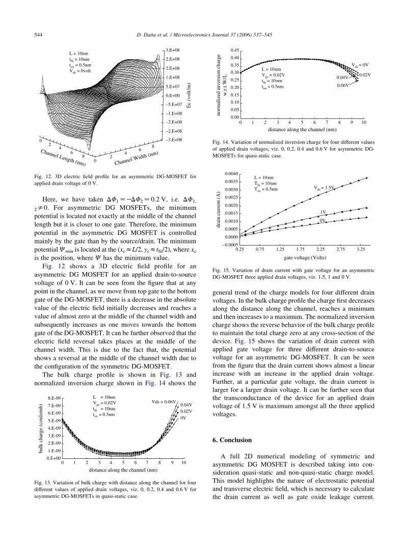
Fig. 12. 3D electric field profile for an asymmetric DG-MOSFET for
applied drain voltage of 0 V.
Fig. 14. Variation of normalized inversion charge for four different values
of applied drain voltages, viz. 0, 0.2, 0.4 and 0.6 V for asymmetric DG-
MOSFETs for quasi-static case.
Fig. 15. Variation of drain current with gate voltage for an asymmetric
DG-MOSFET three applied drain voltages, viz. 1.5, 1 and 0 V.
D. Datta et al. / Microelectronics Journal 37 (2006) 537–545544
Here, we have taken DF1ZKDF2Z0:2 V, i.e. DF1,
2s0. For asymmetric DG MOSFETs, the minimum
potential is located not exactly at the middle of the channel
length but it is closer to one gate. Therefore, the minimum
potential in the asymmetric DG MOSFET is controlled
mainly by the gate than by the source/drain. The minimum
potentialJmin is located at the (xczL/2, ycztSi/2), where xcis the position, where J has the minimum value.
Fig. 12 shows a 3D electric field profile for an
asymmetric DG MOSFET for an applied drain-to-source
voltage of 0 V. It can be seen from the figure that at any
point in the channel, as we move from top gate to the bottom
gate of the DG-MOSFET, there is a decrease in the absolute
value of the electric field initially decreases and reaches a
value of almost zero at the middle of the channel width and
subsequently increases as one moves towards the bottom
gate of the DG-MOSFET. It can be further observed that the
electric field reversal takes places at the middle of the
channel width. This is due to the fact that, the potential
shows a reversal at the middle of the channel width due to
the configuration of the symmetric DG-MOSFET.
The bulk charge profile is shown in Fig. 13 and
normalized inversion charge shown in Fig. 14 shows the
Fig. 13. Variation of bulk charge with distance along the channel for four
different values of applied drain voltages, viz. 0, 0.2, 0.4 and 0.6 V for
asymmetric DG-MOSFETs in quasi-static case.
general trend of the charge models for four different drain
voltages. In the bulk charge profile the charge first decreases
along the distance along the channel, reaches a minimum
and then increases to a maximum. The normalized inversion
charge shows the reverse behavior of the bulk charge profile
to maintain the total charge zero at any cross-section of the
device. Fig. 15 shows the variation of drain current with
applied gate voltage for three different drain-to-source
voltage for an asymmetric DG-MOSFET. It can be seen
from the figure that the drain current shows almost a linear
increase with an increase in the applied drain voltage.
Further, at a particular gate voltage, the drain current is
larger for a larger drain voltage. It can be further seen that
the transconductance of the device for an applied drain
voltage of 1.5 V is maximum amongst all the three applied
voltages.
6. Conclusion
A full 2D numerical modeling of symmetric and
asymmetric DG MOSFET is described taking into con-
sideration quasi-static and non-quasi-static charge model.
This model highlights the nature of electrostatic potential
and transverse electric field, which is necessary to calculate
the drain current as well as gate oxide leakage current.

D. Datta et al. / Microelectronics Journal 37 (2006) 537–545 545
Based on the potential profile, we have achieved the profile
of bulk as well as inversion charges based on symmetric
linearization method. Symmetric linearization also helps us
to reach the essential symmetry with respect to source/drain
interchange, which is a necessary feature of symmetric
DG MOSFETs. In NQS profile, we have derived the
variation of inversion charge with respect to time, where
gate voltage changes with time in a ramp profile or, in 1D
gaussian profile. We have also investigated the expected
Gummel Symmetry in NQS profile. In the present paper, we
have not included the quantum mechanical space quantiza-
tion effect, but the symmetricity of the charge-sheet model
gives the expected behavior of the bulk and inversion charge
density through out the device. This symmetrically
linearized model helps us to derive the transcapacitance
and transconductance profile of both symmetric and
asymmetric DGMOSFET. Finally, scaling limit projections
indicate that individual DG MOSFETs with good turn-off
behavior are feasible at 10 nm scale; however, practical
exploitation of these devices towards giga-scale integrated
systems requires significant improvement in process
control. This model also highlights the device physics
essential to predict the transport phenomena in
DG MOSFETs. The numerical model presented here is
used as tool for simulating modern thin gate DG MOSFETs
used in VLSI circuits.
Acknowledgements
The authors would like to acknowledge the financial
support provided by Ministry of Human Resources and
Development, Govt. of India under Thrust Areas of
Technical Education scheme (No. F27-3/2002TS.V)
References
[1] Y. Taur, C.H. Wann, D. Frank, 25 nm CMOS design considerations,
IEDM Tech. Digest (1998) 789–792.
[2] International Technology Roadmap of Semiconductors, Update, Free
available athttp://www.itrs.net/common/2004update 2004.
[3] D.J. Frank, S. Laux, M. Fischetti, Monte carlo simulation of a 30 nm
dual-gate MOSFET: how short can Si go?, IEDM Tech. Digest (1992)
553–556.
[4] Chen Wanqiang, F.Register Leonard, K.Banerjee Sanjay, Scattering
in a nano-scaleMOSFET: a quantum transport analysis, IEDM (2003).
[5] Brian Winstead, Umberto Ravaioli, A quantum correction based on
schrodinger equation applied to monte carlo device simulation, IEEE
Trans. Electron Dev. 50 (2) (2003) 440–446.
[6] J.A. Lopez-Villanueva, P. Cartujo-Cassinello, F. Gamiz, J. Banqueri,
A.J. Palma, Effects of the inversion layer centroid on the performance
of DG MOSFETs, IEEE Trans. Electron Dev. 47 (1) (2000) 141–146.
[7] Z. Ren, M. Lundstrom, Extraordinarily high drive currents in
asymmetrical DG MOSFETs, Superlattices Microstruct. (2000).
[8] A.R. Boothroyed, S.W Tarasewicz, C. Slabby, MISNAN -A
physically based constant MOSFET model for CAD applications,
IEEE Trans. Electron Dev. 10 (1991) 1512–1529.
[9] G. Baccarani, S. Reggiani, A compact double-gate MOSFET model
comprising quantum-mechanical and nonstatic effects, IEEE Trans.
Electron Dev. 8 (1999) 1656–1666.
[10] Y. Liu, et al. Ultra thin channel vertical DG MOSFET fabricated by
using ion-bombardment-retarded etching, IEEE Trans. on Electron
Devices, Accepted for Future Publication.
[11] Man Wong, Xuejie Shi, On the threshold voltage of symmetrical DG
MOS capacitor with intrinsic silicon body, IEEE Trans. Electron Dev.
51 (2004) 1600–1604.
[12] M. Miura-Mattausch, W. Feldmann, A.R. Ahm, M. Bollu,
D. Savignac, Unified complete MOSFET model for analysis of digital
and analog circuits, IEEE Trans. Comput-Aid Design 15 (1996) 1–7.
[13] K. Joardar, K. Joardar, K.K. Gullapalli, C.C. McAndrew,
M.E. Burnham, A. Wild, An improved MOSFET model for circuit
simulation, IEEE Trans. Electron Dev. 45 (1) (1998) 134–148.
[14] Xiaoping Liang, Y. Taur, A 2-D analytical solution for SCEs in DG
MOSFETs, IEEE Trans. Electron Dev. 51 (2004) 1385–1391.
[15] J.R. Brews, A charge sheet model for MOSFET, Solid State Electron
21 (1978) 345–355.
[16] D.E. Ward, R.W. Dutton, A charge oriented model for MOS transistor
capacitances, IEEE J. Solid State circuits SC-13 (1978) 703–708.
[17] S. Dasgupta, P. Chakrabarti, Effect of ionising radiation on the
characteristics of a MOSFET, IEE Circ. Dev. Syst. 147 (2000) 133–
138.
[18] T.L. Chen, G. Gildenblat, Symmetric bulk charge linearization in
charge-sheet MOSFET model, Electron Lett. 37 (2001) 791–793.
[19] C.C. Enz, MOS transistor modeling dedicated to low current and low
voltage analog circuit design and simulation Presented at Sixth
Brazilian School of Microelectronics, May 1996.
[20] Cunha, et al., An explicit physical model for long channel MOS
transistor including small signal parameters, Solid State Electron 38
(1995) 1945–1952.