TWO-CELL,THREE-CELL,AND FOUR …€¢ Provides Individual Cell Voltages ... observe and control the...
39
PW RTH www.ti.com FEATURES APPLICATIONS DESCRIPTION SYSTEM PARTITIONING DIAGRAM LDO, Therm Output Drive & UVLO Power Management LDO, TOUT, and Power Mode control I 2 C Capacity Prediction <1% Error SMBus Pack + Pack - Discharge / Charge / Precharge FETs Cell and Pack Voltage Measurement Precharge FET Drive 2-Tier Overcurrent Protection 32-kHz Clock Generator bq2084 768 Bytes of User Flash Fuse 1 st Level OV and UV Protection Pack Undervoltage Power Mode Control Precharge Control Delay Counters Cell Balancing Algorithm and Control Cell Balancing Drive System Interface System Watchdog Voltage Level Translator System Interface 32 kHz Power Mode Control Fail-Safe Protection T1 1 st Level OC Protection Temperature Measurement <1% Error T INT Supply V oltage bq29312A PCH FET Drive RAM Registers SBS v1.1 Data bq29312 RAM/Comms Validation 2 nd Level Overvolt age Protection XAlert Sleep Sense Resistor (10 - 30 m W) PF Input bq29312A SLUS629A – JANUARY 2005 – REVISED AUGUST 2005 TWO-CELL, THREE-CELL, AND FOUR-CELL LITHIUM-ION OR LITHIUM-POLYMER BATTERY PROTECTION AFE • Notebook PCs • 2-, 3-, or 4-Cell Series Protection Control • Medical and Test Equipment • Can Directly Interface With the bq2084 Gas • Portable Instrumentation Gauges • Provides Individual Cell Voltages and Battery Voltage to Battery Management Host The bq29312A is a 2-, 3-, or 4-cell lithium-ion battery • Integrated Cell Balancing Drive pack protection analog front end (AFE) IC that • I 2 C Compatible User Interface Allows Access incorporates a 3.3-V, 25-mA low-dropout regulator to Battery Information (LDO). The bq29312A also integrates an I 2 C compat- • Programmable Threshold and Delay for ible interface to extract battery parameters such as Overload and Short Circuit During Charge and cell voltages and control output status. Other par- Discharge ameters such as current protection thresholds and delays can be programmed into the bq29312A to • System Alert Interrupt Output increase the flexibility of the battery management • Host Control Can Initiate Sleep Power Mode system. and Ship Mode The bq29312A provides safety protection for over- • Integrated 3.3-V, 25-mA LDO charge, overload, short-circuit, overvoltage, and • Supply Voltage Range From 4.5 V to 25 V undervoltage conditions with the battery management host. In overload and short-circuit conditions, the • Low Supply Current of 60-μA Typical bq29312A turns the FET drive off autonomously • bq29312A is 100% specification compatible dependant on the internal configuration setting. with the bq29312 Please be aware that an important notice concerning availability, standard warranty, and use in critical applications of Texas Instruments semiconductor products and disclaimers thereto appears at the end of this data sheet. PRODUCTION DATA information is current as of publication date. Copyright © 2005, Texas Instruments Incorporated Products conform to specifications per the terms of the Texas Instruments standard warranty. Production processing does not necessarily include testing of all parameters.
Transcript of TWO-CELL,THREE-CELL,AND FOUR …€¢ Provides Individual Cell Voltages ... observe and control the...

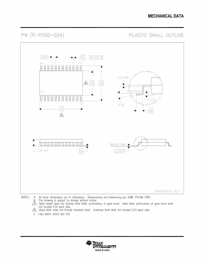
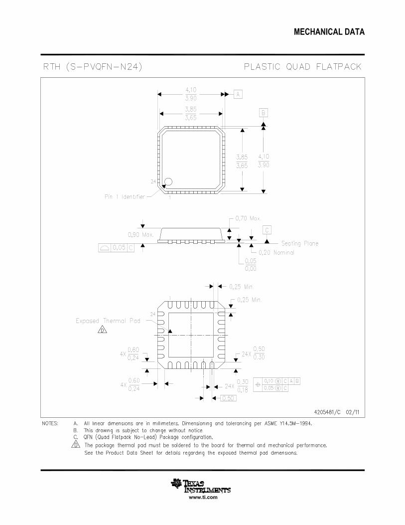
PW RTH
www.ti.com
FEATURES APPLICATIONS
DESCRIPTION
SYSTEM PARTITIONING DIAGRAM
LDO, Therm Output Drive & UVLO
Power ManagementLDO, TOUT, and Power Mode control
I2C
Capacity Prediction <1% Error
SMBus
Pack +
Pack -
Discharge / Charge /
Precharge FETs
Cell and Pack
Voltage
Measurement
Precharge
FET Drive
2-Tier Overcurrent Protection
32-kHz Clock
Generator
bq2084
768 Bytes of
User Flash
Fuse
1stLevel OV andUV Protection
Pack Undervoltage
Power Mode
Control
Precharge Control
Delay Counters
Cell Balancing Algorithm and Control
Cell Balancing
Drive
System Interface
System Watchdog
Voltage Level Translator
System Interface
32 kHz
Power Mode Control
Fail-Safe Protection
T1
1stLevel OCProtection
Temperature Measurement
<1% ErrorTINT
Supply V oltage
bq29312A
PCH FET Drive
RAM RegistersSBS v1.1 Data
bq29312 RAM/Comms Validation
2 n
d L
eve
l O
ve
rvo
lta
ge P
rote
ctio
n
XAlert
Sleep
Sense Resistor
(10 - 30 m W)
PF Input
bq29312ASLUS629A–JANUARY 2005–REVISED AUGUST 2005
TWO-CELL, THREE-CELL, AND FOUR-CELL LITHIUM-ION ORLITHIUM-POLYMER BATTERY PROTECTION AFE
• Notebook PCs• 2-, 3-, or 4-Cell Series Protection Control• Medical and Test Equipment• Can Directly Interface With the bq2084 Gas• Portable InstrumentationGauges
• Provides Individual Cell Voltages and BatteryVoltage to Battery Management Host
The bq29312A is a 2-, 3-, or 4-cell lithium-ion battery• Integrated Cell Balancing Drivepack protection analog front end (AFE) IC that• I2C Compatible User Interface Allows Accessincorporates a 3.3-V, 25-mA low-dropout regulatorto Battery Information(LDO). The bq29312A also integrates an I2C compat-
• Programmable Threshold and Delay for ible interface to extract battery parameters such asOverload and Short Circuit During Charge and cell voltages and control output status. Other par-Discharge ameters such as current protection thresholds and
delays can be programmed into the bq29312A to• System Alert Interrupt Outputincrease the flexibility of the battery management• Host Control Can Initiate Sleep Power Mode system.
and Ship ModeThe bq29312A provides safety protection for over-• Integrated 3.3-V, 25-mA LDOcharge, overload, short-circuit, overvoltage, and
• Supply Voltage Range From 4.5 V to 25 V undervoltage conditions with the battery managementhost. In overload and short-circuit conditions, the• Low Supply Current of 60-µA Typicalbq29312A turns the FET drive off autonomously• bq29312A is 100% specification compatibledependant on the internal configuration setting.with the bq29312
Please be aware that an important notice concerning availability, standard warranty, and use in critical applications of TexasInstruments semiconductor products and disclaimers thereto appears at the end of this data sheet.
PRODUCTION DATA information is current as of publication date. Copyright © 2005, Texas Instruments IncorporatedProducts conform to specifications per the terms of the TexasInstruments standard warranty. Production processing does notnecessarily include testing of all parameters.

www.ti.com
DESCRIPTION (Continued)
PACKAGE DISSIPATION RATINGS
ABSOLUTE MAXIMUM RATINGS
bq29312ASLUS629A–JANUARY 2005–REVISED AUGUST 2005
These devices have limited built-in ESD protection. The leads should be shorted together or the deviceplaced in conductive foam during storage or handling to prevent electrostatic damage to the MOS gates.
The communications interface allows the host to observe and control the current status of the bq29312A. Itenables cell balancing, enters different power modes, sets overload levels, sets the overload blanking delay time,sets short-circuit threshold levels for charge and discharge, and sets the short-circuit blanking delay time.
Cell balancing of each cell is performed via a cell bypass path, which is enabled via the internal control registeraccessible via the I2C compatible interface. The maximum bypass current is set via an external series resistorand internal FET on resistance (typical 400 Ω).
ORDERING INFORMATION (1)
PACKAGEDTA
TSSOP (PW) (2) QFN (RTH) (3)
–40°C to 85°C bq29312APWR-SA bq29312ARTH
(1) For the most current package and ordering information, see the Package Option Addendum at the end of this document, or see the TIwebsite at www.ti.com.
(2) The bq29312A can be ordered in tape and reel by adding the suffix R to the orderable part number, ie: bq29312APWR bq29312ARTHR.(3) The QFN package is also made available in mini reel, add suffix T to the orderable part number, ie: bq29312ARTHT.
POWER RATINGPOWER RATING DERATING FACTORPACKAGE TA ≤ 25°C ABOVE TA ≤ 25°C TA ≤ 70°C TA = 85°C
PW 874 mW 6.99 W/°C 559 mW 454 mW
over operating free-air temperature range unless otherwise noted (1) (2)
bq29312A
VCC Supply voltage range PACK, BAT –0.3 V to 34 V
VC1, VC2, VC3, VC4 –0.3 V to 34 V
SR1, SR2 –1.0 V to 1.0 V
VC5 –1.0 V to 4.0 VVI Input voltage range VC1 to VC2, VC2 to VC3, VC3 to VC4, VC4 to –0.3 to 8.5 VVC5
WDI, SLEEP, SCLK, SDATA –0.3 to 8.5 V
ZVCHG –0.3 V to 34 V
DSG, CHG –0.3 V to BAT
OD –0.3 V to 34 VVO Output voltage range
PMS –0.3 V to PACK–0.2 V
TOUT, SCLK, SDATA, CELL, XALERT –0.3 to 7 V
Current for cell balancing 10 mA
Continuous total power dissipation See Dissipation Rating Table
Tstg Storage temperature range –65°C to 150°C
Lead temperature (soldering, 10 s) 300°C
(1) Stresses beyond those listed under "absolute maximum ratings" may cause permanent damage to the device. These are stress ratingsonly, and functional operation of the device at these or any other conditions beyond those indicated under "recommended operatingconditions" is not implied. Exposure to absolute-maximum-rated conditions for extended periods may affect device reliability.
(2) All voltages are with respect to ground of this device except VCn–VC(n+1), where n = 1-, 2-, 3-, 4-cell voltage.
2

www.ti.com
RECOMMENDED OPERATING CONDITIONS
bq29312ASLUS629A–JANUARY 2005–REVISED AUGUST 2005
MIN NOM MAX UNIT
Supply Voltage (BAT or PACK) 4.5 (1) 25 V
VI(STARTUP) Start-up voltage (PACK) 5.0 V
VC1, VC2, VC3, VC4 0 BAT
SR1, SR2 –0.5 0.5
VC5 –0.5 3.0VI Input voltage range V
VCn – VC(n+1), (n = 1, 2, 3, 4 ) 0 5.0
PMS 0 PACK
SLEEP 0 REG
VIH 0.8 × REG REG VLogic level input voltage SCLK, SDATA, WDI
VIL 0 0.2 × REG
VIH V(PACK) – 0.2 V(PACK) VPMS logic level PMS
VIL 0 0.2
PMS pullup/pulldown resistance RPMS 100 1000 kΩ
VO Output voltage OD 25 V
IO Output current XALERT, SDATA 200 µA
CELL ±10 µAInput current,II SLEEP -0.5 1.0 µAExternal 3.3-V REG capacitor
C(REG) 4.7 µF
R(CELL) 100 ΩExtend CELL output filter
C(CELL) 100 nF
OD 1 mAIOL Input frequency
WDI 32.768 kHz
WDI high time 2 28 µs
TA Operating temperature –40 85 °C
(1) V(PACK) supply voltage must rise above start-up voltage on power up to enable the internal regulator which drives REG and TOUT asrequired. Once V(PACK) is above the start-up voltage, it can fall down to the minimum supply voltage and still meet the specifications ofthe bq29312A.
3

www.ti.com
ELECTRICAL CHARACTERISTICS
bq29312ASLUS629A–JANUARY 2005–REVISED AUGUST 2005
TA = 25°C, C(REG) = 4.7 µF, BAT = 14 V (unless otherwise noted)
PARAMETER TEST CONDITIONS MIN TYP MAX UNIT
SUPPLY CURRENT
No load at REG, TOUT, XALERT, SCLK, and SDATA. 60 90ICC1 Supply current 1 ZVCHG = off ,VMEN = on, WDI no clock, µA
TA = –25°C to 85°C 100Select VC5 = VC4 = 0 V
Supply current No load at REG, TOUT, XALERT, SCLK, and SDATA.ICC2 2(Depends of VM TA = –25°C to 85°C 25 50 µAZVCHG = off, VMEN = off, WDI no clocktopology selected)
No load at REG, TOUT, XALERT, SCLK, andI(SLEEP) Sleep current SDATA.CHG, DSG and ZVCHG = off, REG = on, TA = –25°C to 85°C 20 40 µA
VMEN = off, WDI no clock, SLEEP = REG or OPEN
REG, CHG, DSG and ZVCHG = off, REG = off,I(SHIP) Ship current TA = –25°C to 85°C 0.1 1.0 µAVMEN = off, WDI no clock, VPACK= 0 V
3.3 V LDO
8.0 V < BAT or PACK ≤ 25 V, IOUT ≤ 25 mA –4% 3.3 2%V
6.5 V < BAT or PACK ≤ 8 V, IOUT ≤ 25 mA –9% 3.3 2%Regulator outputV(REG) TA = –25°C to 85°Cvoltage 5.4 V ≤ BATor PACK ≤ 6.5 V, IO ≤ 16 mA –9% 3.3 2% V
4.5 V ≤ BAT or PACK ≤ 25 V, IO ≤ 2 mA –2% 3.3 2% V
Regulator output∆V(EGTEMP) change with 5.4 V ≤ BAT ≤ 25 V, IO = 2 mA, TA = –25°C to 85°C ±0.2%
temperature
∆V(REGLINE) Line regulation 5.4 V ≤ BAT or PACK ≤ 25 V, IO = 2 mA 10 20 mV
BAT = 14 V, 0.2 mA ≤ IO ≤ 2 mA 7 15∆V(REGLOAD) Load regulation mV
BAT = 14 V, 0.2 mA ≤ IO ≤ 25 mA 40 100
BAT = 14 V, REG = 3 V 25 100IMAX Current limit mA
BAT = 14 V, REG = 0 V 12 50
CELL VOLTAGE MONITOR
V(Cn) – V(Cn + 1) = 0 V, 8 V ≤ BAT or PACK ≤ 25 V 0.975V(CELL OUT) CELL output V
V(Cn) – V(Cn + 1) = 4.5 V, 8 V ≤ BAT or PACK ≤ 25 V 0.3
REF CELL output Mode (1), 8 V ≤ BAT or PACK ≤ 25 V –1% 0.975 1% V
PACK/PACK CELL output Mode (2) –5% 5% V25
K = (CELL output (VC5 = 0 V, VC4 = 4.5 V) –CELL 0.147 0.150 0.153output (VC5 = VC4 = 0 V)/ 4.5K CELL scale factor
K = (CELL output (VC2 = 13.5 V, VC1 = 18 V) –CELL output 0.147 0.150 0.153(VC2 = VC1 = 13.5 V)/ 4.5
CELL output offsetVICR CELL output (VC2 = 17 V, VC1 = 17 V) CELL output (VC2 = VC1 = 0 V) –1 mVerror
Cell balance internalR(BAL) rds(ON) for internal FET switch at VDS = 2 V 200 400 800 Ωresistance
(1) Register Address =0x04, b2(CAL0) = b3(CAL1) = 1, Register Address = 0x03, b0(VMEN) = 1(2) Register Address = 0x03, b1(PACKOUT) = 1, b0( VMEN) = 1
4

www.ti.com
ELECTRICAL CHARACTERISTICS (Continued)
bq29312ASLUS629A–JANUARY 2005–REVISED AUGUST 2005
TA = 25°C, C(REG) = 4.7 µF, BAT = 14 V (unless otherwise noted)
PARAMETER TEST CONDITION MIN NOM MAX UNIT
OVERLOAD (OL) AND SHORT-CIRCUIT (SC) DETECTION
VOL OL detection threshold range, typical (1) –50 –205 mV
∆VOL OL detection threshold program step 5 mV
VHYS(OL) OL detection threshold hysteresis 7 10 13 mV
Charge 100 475V(SC) SC detection threshold range, typical (2) mV
Discharge –100 –475
Charge 25∆V(SC) SC detection threshold program step mV
Discharge –25
VHYS(SC) SC detection threshold hysteresis Charge and Discharge 40 50 60 mV
VOL = 50 mV (min) 40 50 60
V(OL_acr) OL detection threshold accuracy (1) Discharge VOL = 100 mV 90 100 110 mV
VOL = 205 mV (max) 184 205 226
VSC = 100 mV (min) 80 100 120
V(SC_acr) SC detection threshold accuracy (2) Charge and Discharge VSC = 200 mV 180 200 220 mV
VSC = 475 mV (max) 426 475 523
FET DRIVE CIRCUIT
V(FETOND)= V(BAT)– V(DSG)VGS connect 1 MΩ BAT= 20 V 12 15 18Output voltage, charge, and dischargeV(FETON) VFETs on V(FETONC)=V(PACK)– V(CHG)VGS connect 1 MΩ PACK = 20 V 12 15 18
V(ZCHG) ZVCHG clamp voltage PACK= 4.5 V 3.3 3.5 3.7 V
V(FETOFF)= V(PACK)– V(DSG) PACK= 16 V 0.2Output voltage, charge and dischargeV(FETOFF) VFETs off V(FETOFF)=V(BAT)– V(CHG) BAT = 16 V 0.2
VDSG :10%–90% 40 200tr Rise time CL = 4700 pF µs
VCHG :10%–90% 40 200
VDSG :90%–10% 40 200tf Fall time CL = 4700 pF µs
VCHG :90%–10% 40 200
THERMISTOR DRIVE
IO = –1 mA at TOUT pin, rds(ON) = (VREG– VO (TOUT))/1 mA,rDS(on) TOUT pass-element series resistance 50 100 ΩTA = –25°C to 85°C
LOGIC
XALERT TA = –25°C to 85°C 60 100 200R(PUP) Internal pullup resistance kΩ
SDATA, SCLK, TA = –25°C to 85°C 6 10 20
XALERT, IO = 200 µA, TA = –25°C to 85°C 0.2
VOL Logic level output voltage SDATA, IO = 50 µA, TA = –25°C to 85°C 0.4 V
OD IO=1 mA, TA = –25°C to 85°C 0.6
(1) See OL register for setting detection threshold(2) See SC register for setting detection threshold
5

www.ti.com
AC ELECTRICAL CHARACTERISTICS
AC TIMING SPECIFICATIONS (I2C COMPATIBLE SERIAL INTERFACE)
tsu(STA)
SCLK
SDATA
SCLK
SDATA
SCLK
SDATA
tw(H) tw(L) tf tr
tr tf
StartCondition SDA
InputSDAChange
StopCondition
th(STA)th(DAT) tsu(DAT)
th(ch)
Start Condition tv
1 2 3 7 8 9
MSB ACK
Stop Condition
tsu(STOP)
1 2 3 7 8 9
MSB ACK
tsu(BUF)
bq29312ASLUS629A–JANUARY 2005–REVISED AUGUST 2005
TA = 25°C, C(REG) = 4.7 µF, BAT = 14 V (unless otherwise noted)
PARAMETER TEST CONDITION MIN NOM MAX UNIT
t(WDTINT) WDT start-up detect time 250 700 2000 ms
t(WDWT) WDT detect time 100 µs
PARAMETER MIN MAX UNIT
tr SCLK SDATA rise time 1000 ns
tf SCLK SDAT fall time 300 ns
tw(H) SCLK pulse width high 4.0 µs
tw(L) SCLK pulse width low 4.7 µs
tsu(STA) Setup time for START condition 4.7 µs
th(STA) START condition hold time after which first clock pulse is generated 4.0 µs
tsu(DAT) Data setup time 250 ns
th(DAT) Data hold time 0 µs
tsu(STOP) Setup time for STOP condition 4.0 µs
tsu(BUF) Time the bus must be free before new transmission can start 4.7 µs
t V Clock low to data out valid 900 ns
th(CH) Data out hold time after clock low 0 ns
fSCL Clock frequency 0 100 kHz
6
www.ti.com
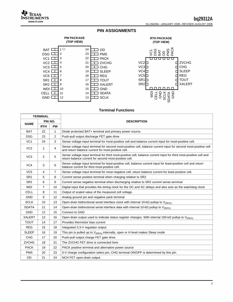
PIN ASSIGNMENTS
123
4 56789
101112
242322
212019181716
151413
BATDSGVC1VC2VC3VC4VC5SR1SR2WDI
CELLGND
ODPMSPACKZVCHGCHGSLEEPREGTOUTXALERTGNDSDATASCLK
PW PACKAGE(TOP VIEW)
BA
TD
SG
VC
1
VC3VC4
SR2SR1VC5
GN
D
XALERT
REGTOUT
ZVCHG
PA
CK
OD
WD
IC
ELL
SD
ATA
GN
D
VC2
SC
LK
SLEEPCHG
PM
S
RTH PACKAGE(TOP VIEW)
bq29312ASLUS629A–JANUARY 2005–REVISED AUGUST 2005
Terminal Functions
TERMINAL
PIN NO. DESCRIPTIONNAME
RTH PW
BAT 22 1 Diode protected BAT+ terminal and primary power source.
DSG 23 2 Push-pull output discharge FET gate drive
VC1 24 3 Sense voltage input terminal for most-positive cell and balance current input for most-positive cell.
Sense voltage input terminal for second most-positive cell, balance current input for second most-positive cellVC2 1 4 and return balance current for most-positive cell.
Sense voltage input terminal for third most-positive cell, balance current input for third most-positive cell andVC3 2 5 return balance current for second most-positive cell.
Sense voltage input terminal for least-positive cell, balance current input for least-positive cell and returnVC4 3 6 balance current for third most-positive cell.
VC5 4 7 Sense voltage input terminal for most-negative cell, return balance current for least-positive cell.
SR1 5 8 Current sense positive terminal when charging relative to SR2
SR2 6 9 Current sense negative terminal when discharging relative to SR2 current sense terminal
WDI 7 10 Digital input that provides the timing clock for the OC and SC delays and also acts as the watchdog clock.
CELL 8 11 Output of scaled value of the measured cell voltage.
GND 9 12 Analog ground pin and negative pack terminal
SCLK 10 13 Open-drain bidirectional serial interface clock with internal 10-kΩ pullup to V(REG).
SDATA 11 14 Open-drain bidirectional serial interface data with internal 10-kΩ pullup to V(REG).
GND 12 15 Connect to GND
XALERT 13 16 Open-drain output used to indicate status register changes. With internal 100-kΩ pullup to V(REG)
TOUT 14 17 Provides thermistor bias current
REG 15 18 Integrated 3.3-V regulator output
SLEEP 16 19 This pin is pulled up to V(REG) internally, open or H level makes Sleep mode
CHG 17 20 Push-pull output charge FET gate drive
ZVCHG 18 21 The ZVCHG FET drive is connected here
PACK 19 22 PACK positive terminal and alternative power source
PMS 20 23 0-V charge configuration select pin, CHG terminal ON/OFF is determined by this pin.
OD 21 24 NCH FET open-drain output
7
www.ti.com
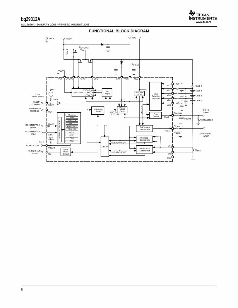
GND
CE
LL
1..
4
SR1
SR2
OverloadComparator
Short-Circuit
SHORT-CIRCUIT
DELAY
Open-DrainOutput
WatchdogTimer
OD
Cell VoltageTranslation
PowerModeCircuit
DriveControl
VCELL
RSNS
RCELL
CCELL
TOUT
RTHERM
CTHERMTHERMISTOR
CellSelectionSwitches
3.3V LDOPOR
SHIP_ON
SLEEP_ON
BAT PACK REG
C(REG)
FETLogic
Gate Driver CHG_ON
DSG_ON
ZVCHG_ON
DSGCHGZVCHG
PACK- PACK+
R(ZVCHG)
PMS
GG VDD
VC1
VC2
VC5
CELL 3
CELL 4
VC3
VC4 CELL 1
CELL 2
GG TS
INPUT
GG ANALOG
INPUT
SLEEP
REG
WDI
SLEEP
CONTROL
32-kHz INPUT
FROM GG
GG INTERFACE
SDATA
ALERT TO GG
OPEN-DRAIN
OUTPUT
GG INTERFACE
SCLK
SDATA
SCLK
XALERT
SE
RIA
LIN
TE
RF
AC
E
Status
Output Ctl
State Ctl
Function Ctl
CELL_SEL
OCDV
OCDT
SCC
SCD
Registers
Comparator
OVERCURRENT
REG
200 k
200 k
0.2-ACurrent Source
_+
-
bq29312ASLUS629A–JANUARY 2005–REVISED AUGUST 2005
FUNCTIONAL BLOCK DIAGRAM
8

www.ti.com
No Power
POWER SUPPLY TO PACK
FETS: OFF(*2)REG: start WorkingI2C: OFFCURRENT FAULT : OFF
CELL MONITOR : OFFWATCHDOG : OFFTHERMISTOR PWER CTRL : OFF
INITIALIZE
FETS: OFFREG: ONI2C: ONCURRENT FAULT : OFF
CELL MONITOR : OFFWATCHDOG : ONTHERMISTOR PWER CTRL : OFF
HOST FAULT MODE
REG >2.4 V REG < 2.3 V
FETS: ON *2REG: ONI2C: ONCURRENT FAULT : ON
CELL MONITOR : ONWATCHDOG : ONTHERMISTOR PWER CTRL : ON
NORMAL MODE
RESET WDTF LATCH
HOST CLOCK STOP
STATE CTL REGISTER b1 = 1
AND NO SUPPLY POWER TO PACK
FETS: OFFREG: ONI2C: ONCURRENT FAULT : OFF
CELL MONITOR : OFFWATCHDOG : OFFTHERMISTOR PWER CTRL : OFF
SLEEP MODE
SLEEP MODE EXIT BY
STATE CTL REGISTER b0 = 0
AND SLEEP PIN = GND
*1
FETS: OFFREG: OFFI2C: OFFCURRENT FAULT : OFF
CELL MONITOR : OFFWATCHDOG : OFFTHERMISTOR PWER CTRL : OFF
SHIP MODE
SHIP MODE SET BY STATE CTL REGISTER
b1 = 1 AND NO SUPPLY POWER TO PACK
FETS: OFFREG: ONI2C: ONCURRENT FAULT : ON
CELL MONITOR : ONWATCHDOG : ONTHERMISTOR PWER CTRL : ON
CURRENT DETECT MODE
STATE CTL REGISTER b0 = 1
or SLEEP PIN = REG or OPEN
*1
RESET CURRENT LATCH
IFAULT
SHIP MODE SET BY
STATE CTL REGISTER
b1 = 1 AND NO SUPPLY
POWER TO PACK
Interrupt Request When
Enrering These States
*1: Interrupt Request is Granted When Only External Sleep Pin Changes
*2: When PMS connect to Pack, Default State of CHG FET is ON.
SHIP MODE EXIT BY POWER
SUPPLY TO PACK
bq29312ASLUS629A–JANUARY 2005–REVISED AUGUST 2005
STATE DIAGRAM
9

www.ti.com
FUNCTIONAL DESCRIPTION
Low-Dropout Regulator (REG)
Initialization
Overload Detection
Short-Circuit Detection
Overload and Short-Circuit Delay
Overload and Short-Circuit Response
bq29312ASLUS629A–JANUARY 2005–REVISED AUGUST 2005
The inputs for this regulator can be derived from the battery cell stack (BAT) or the pack positive terminal(PACK). The output is typically 3.3 V with the minimum output capacitance for stable operation is 4.7 µF and isalso internally current limited. During normal operation, the regulator limits output current to typically 50 mA.
The bq29312A internal control circuit is powered by the REG voltage, which it also monitors. When the voltage atREG falls below 2.3 V, the internal circuit turns off the FETs and disables all controllable functions, including theREG and TOUT outputs. REG does not start up unless a voltage above V(STARTUP) is supplied to the PACKterminal. After the regulator has started, based on PACK voltage, it keeps operating through the BAT input, evenif the PACK voltage is removed. If the BAT input is below the minimum operating range, then the bq29312A doesnot operate if the supply to the PACK input is removed. After start up, when the REG voltage is above 2.4 V, thebq29312A is in Normal mode.
The initial state of the CHG output depends on the PMS input. If PMS = PACK, then CHG = ON, however, ifPMS = GND, then CHG = OFF.
The overload detection is used to detect abnormal currents in the discharge direction. This feature is used toprotect the pass FETs, cells and any other inline components from excessive current conditions. The detectioncircuit also incorporates a blanking delay before driving the control for the pass FETs to the OFF state. Theoverload sense voltage is set in the OLV register, and delay time is set in the OLT register. The overloadthreshold can be programmed from 50 mV to 205 mV in 5-mV steps with the default being 50 mV and hysteresisof 10 mV.
The short current circuit detection is used to detect abnormal current in either the charge or discharge direction.This safety feature is used to protect the pass FETs, cells, and any other inline components from excessivecurrent conditions. The detection circuit also incorporates a blanking delay before driving the control for the passFETs to the OFF state. The short-circuit thresholds and delay time are set in the SCC and SCD registers,respectively, where SCC is for charging and SCD is for discharge. The short-circuit threshold can beprogrammed from 100 mV to 475 mV in 25-mV steps with the default being 100 mV and hysteresis of 50 mV.
The overload delay (default =1 ms) allows the system to momentarily accept a high current condition withoutdisconnecting the supply to the load. The delay time can be increased via the OLT register, which can beprogrammed for a range of 1 ms to 31 ms with steps of 2 ms.
The short-circuit delay (default = 0 µs) is programmable in the SCC and SCD registers. This register can beprogrammed from 0 µs to 915 µs with steps of 61 µs.
When an overload or short-circuit fault is detected, the FETs are turned off. The STATUS (b0…b2) registerreports the details of short-circuit (charge), short-circuit (discharge), and overload. The respective STATUS(b0…b2) bits are set to 1 and the XALERT output is triggered. This condition is latched until the CONTROL (b0)is set and then reset. If a FET is turned on via resetting CONTROL (b0) and the error condition is still present onthe system, then the device reenters the protection response state.
10

www.ti.com
Cell Voltage
Calibration of Cell Voltage Monitor Amplifier Gain
bq29312ASLUS629A–JANUARY 2005–REVISED AUGUST 2005
FUNCTIONAL DESCRIPTION (continued)
The cell voltage is translated to allow a system host to measure individual series elements of the battery. Theseries element voltage is translated to a GND-based voltage equal to 0.15 ±0.002 of the series element voltage.This provides a range from 0 V to 4.5 V. The translation output is inversely proportional to the input using thefollowing equation.
Where, V(CELL OUT) = –K × V(CELL IN) + 0.975 (V)
Programming CELL_SEL (b1, b0) selects the individual series element. The CELL_SEL (b3, b2) selects thevoltage monitor mode, cell monitor, offset, etc.
The cell voltage monitor amplifier has an offset, and to increase accuracy, this can be calibrated.
There are a couple of methods by calibration circumstance.
The following procedure shows how to measure and calculate the offset and gain as an example.• Step 1
– Set CAL1=1, CAL0=1, CELL1=0, CELL0=0, VMEN=1– VREF is trimmed to 0.975 V within ±1%, measuring VREF eliminates its error.– Measure internal reference voltage VREF from VCELL directly.– VREF=measured reference voltage
• Step 2– Set CAL1=0, CAL0=0, CELL1=0, CELL0=1, VMEN=1– The output voltage includes the offset and represented by:
VO(4-5) = VREF + (1 + K) × VOS (V)Where K = CELL Scaling Factor
– VOS = Offset voltage at input of the internal operational amplifier• Step 3
– Set CAL1=1, CAL0=0, CELL1=0, CELL0=0, VMEN=1– Measuring scaled REF voltage through VCELL amplifier.– The output voltage includes the scale factor error and offset and is represented by:
V(OUTR) = VREF + (1 + K) × VOS– K × VREF (V)• Step 4
– Calculate (VO(4-5)– V(OUTR)/VREF
– The result is the actual scaling factor, K(ACT), and is represented by:K(ACT) = (VO(4-5)– V(OUTR))/VREF = (VREF + (1 + K) × VOS) - (VREF + (1 + K) × VOS– K × VREF)/ VREF = K ×VREF/VREF = K
• Step 5– Calculate the actual offset value where:
VOS(ACT) = (VO(4-5)– VREF)/(1 + K(ACT))• Step 6
– Calibrated cell voltage is calculated by:VCn – VC(n+1) = VREF + (1 + K(ACT) ) × VOS(ACT) – V(CELLOUT)/K(ACT) – VO(4-5) – V(CELLOUT)/K(ACT)
For improved measurement accuracy, VOS(ACT) for each cell voltage should be measured.• Set CAL1=0, CAL0=0, CELL1=0, CELL0=1, VMEN=1• Set CAL1=0, CAL0=0, CELL1=1, CELL0=0, VMEN=1• Set CAL1=0, CAL0=0, CELL1=1, CELL0=1, VMEN=1
11

www.ti.com
Cell Balance Control
Thermistor Drive Circuit (TOUT)
Open-Drain Drive Circuit (OD)
XALERT (XALERT)
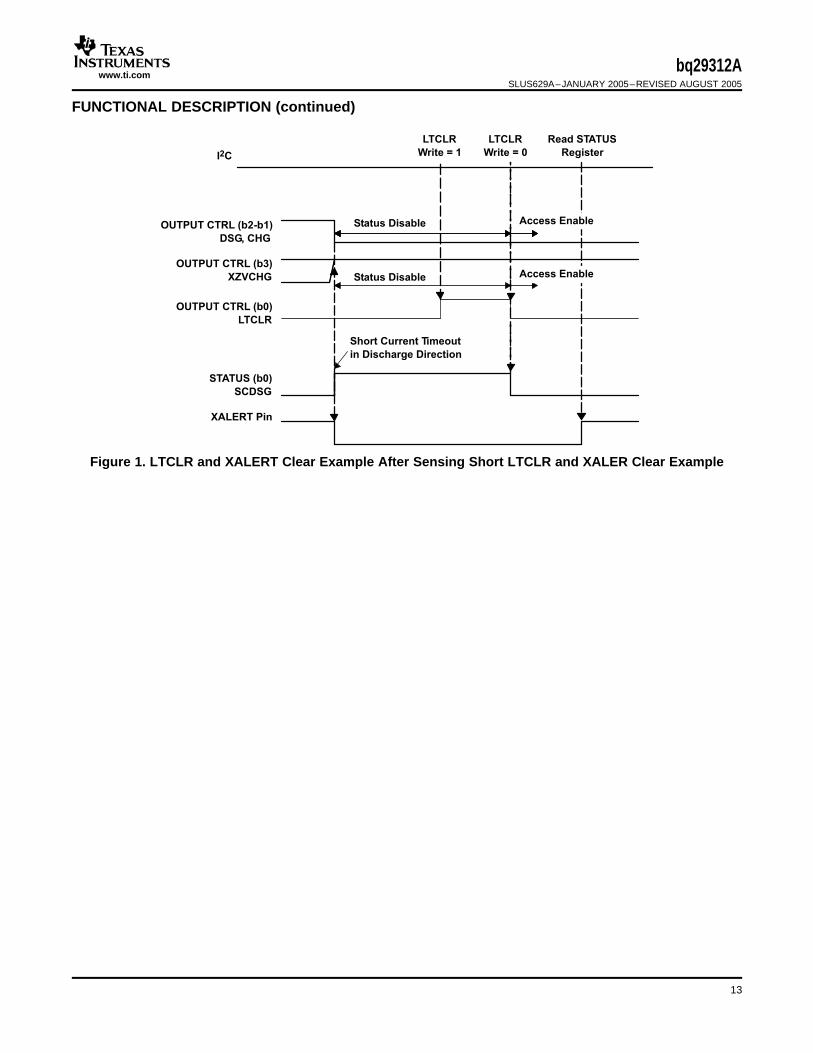
Latch Clear (LTCLR)
bq29312ASLUS629A–JANUARY 2005–REVISED AUGUST 2005
FUNCTIONAL DESCRIPTION (continued)
Measuring VO(3-4) , VO(2-3), VO(1-2),
• VC4 – VC5 = VO(4-5)– V(CELLOUT)/ K(ACT)
• VC3 – VC4 = VO(3-4)– V(CELLOUT)/ K(ACT)
• VC2 – VC3 = VO(2-3)– V(CELLOUT)/ K(ACT)
• VC1 – VC2 = VO(1-2)– V(CELLOUT)/ K(ACT)
The cell balance control allows a small bypass path to be controlled for any one series element. The purpose ofthis bypass path is to reduce the current into any one cell during charging to bring the series elements to thesame voltage. Series resistors placed between the input pins and the positive series element nodes control thebypass current value. Individual series element selection is made using bits 4 through 7 of the CELL_SELregister.
The TOUT pin can be enabled to drive a thermistor from REG. The typical thermistor resistance is 10 kΩ at25°C. The default-state is OFF to conserve power. The maximum output impedance is 100 Ω. TOUT is enabledin FUNCTION CTL register (bit 5).
The open-drain output has 1-mA current source drive with a maximum output voltage of 25 V. The OD output isenabled or disabled by OUTPUT CTL register (bit 4) and has a default state of OFF.
XALERT is driven low when an OL or SC current fault is detected, if the SLEEP pin changes state or a watchdogfault occurs. To clear XALERT, toggle (from 0, set to 1 then reset to 0) OUTPUT CTL (bit 0), then read theSTATUS register.
When a current limit fault or watchdog timer fault occurs, the state is latched. To clear these faults, toggle (from0, set 1 then reset to 0) LTCLR in the OUTPUT CTL register (bit 0).
Figure 1 is the LTCLR and XALERT clear example after sensing a short-circuit.
12
www.ti.com
I2C
OUTPUT CTRL (b3)
XZVCHG
OUTPUT CTRL (b2-b1)
DSG, CHG
OUTPUT CTRL (b0)
LTCLR
STATUS (b0)
SCDSG
XALERT Pin
LTCLR
Write = 1
LTCLR
Write = 0
Read STATUS
Register
Access EnableAccess Enable
Access Enable
Short Current Timeout
in Discharge Direction
Status Disable
Status Disable
bq29312ASLUS629A–JANUARY 2005–REVISED AUGUST 2005
FUNCTIONAL DESCRIPTION (continued)
Figure 1. LTCLR and XALERT Clear Example After Sensing Short LTCLR and XALER Clear Example
13

www.ti.com
2-, 3-, or 4-Cell Configuration
Watchdog Input (WDI)
GG Clock Never Starts
REG
GG 32-kHz Output
tWDTINT ~ 700 mS
CHG, DSG, and
ZVCHG = OFF
EXT FET Control
GG Clock Stop
CHG, DSG, and
ZVCHG = OFF
tWDWT About 100 mS
REG
GG 32-kHz Output
Watchdog Sense
EXT FET Control
DSG and CHG FET Driver Control
bq29312ASLUS629A–JANUARY 2005–REVISED AUGUST 2005
FUNCTIONAL DESCRIPTION (continued)
In a 3-cell configuration, VC1 is shorted to VC2. In a 2-cell configuration, VC1 and VC2 are shorted to VC3.
The WDI input is required as a time base for delay timing when determining overload and short-circuit delayperiods and is used as part of the system watchdog.
Initially, the watchdog monitors the host oscillator start up; if there is no response from the host within 700 ms ofthe bq29312A reaching its minimum operating voltage, then the bq29312A turns both CHG, DSG, and ZVCHGFETs OFF.
Once the watchdog has been started during this wake-up period, it monitors the host for an oscillation stopcondition, which is defined as a period of 100 µs (typ), where no clock input is received. If an oscillator stopcondition is identified, then the watchdog turns the CHG, DSG, and ZVCHG FETs OFF. When the host clockoscillation is started, WDF is released, but the flag is latched until LTCLR is toggled.
Figure 2. Watchdog Timing Chart—WDI Fault at Startup
Figure 3. Watchdog Timing Chart—WDI Fault After Startup
The bq29312A drives the DSG, CHG, and ZVCHG FET off if an OL or SC safety threshold is breacheddepending on the current direction. The host can force any FET on or off only if the bq29312A integratedprotection control allows. The DSG and CHG FET drive gate-to-drain voltage is clamped to 15 V (typ).
14

www.ti.com
Precharge and 0-V Charging—Theory of Operation
SLEEP Control Input (SLEEP)
Power Modes
bq29312ASLUS629A–JANUARY 2005–REVISED AUGUST 2005
FUNCTIONAL DESCRIPTION (continued)
The default-state of the CHG and DSG FET drive is off, when PMS = GND. A host can control the FET drive byprogramming OUTPUT CTL (b3...b1) where b1 is used to control the discharge FET, b2 is used to control thecharge FET, and b3 is used to control the ZVCHG FET. These controls are only valid when not in the initializedstate. The CHG drive FET can be powered by PACK and the DSG FET can be powered by BAT.
The bq29312A supports both a charger that has a precharge mode and one that does not. The bq29312A alsosupports charging even when the battery falls to 0 V. Detail is described in the application section.
The SLEEP input is pulled-up internally to REG. When SLEEP is pulled to REG, the bq29312A enters theSLEEP mode. The SLEEP mode disables all the FET outputs and the OL, SC, and watchdog faults are alsodisabled. The RAM configuration is still valid on exit of the SLEEP mode. The host can force the bq29312A intoSLEEP mode via register control also.
Table 1. SLEEP Control Input
SLEEPITEM EXIT SLEEP
FUNCTION I2C READ/WRITE
I2C Read/Write Active
REG Output Active
External pin control:
CHG, DSG, ZVCHG, TOUT, OD
OC and SC protection:Write is available, Last pre-sleep entry configuration is valid. (IfSCD, SCC and OCD but read is disabled change configuration, latest write data is valid.)
CELL Translation Disabled
PACKOUT, VMEN
Cell Balancing:
CB[3:0]
Watchdog: WDDIS
The bq29312A has three power modes, Normal, Sleep, and Ship. The following table outlines the operationalfunctions during these power modes.
Table 2. Power Modes
POWER TO EXIT POWERTO ENTER POWER MODE MODE DESCRIPTIONMODE MODE
The battery is in normal operation with protection, powermanagement, and battery monitoring functions available andSLEEP = GND andoperating.Normal STATE CTL( b0) = 0 and
STATE CTL( b1) = 0 The supply current of this mode varies as the host can enableand disable various power management features.
All functions stop except LDO and I2C interface.
SLEEP = REG (floating) or On entry to this mode, all registers are masked off keepingSLEEP = GND andSleep STATE CTL( b0) = 1 and their state.STATE CTL( b0) = 0STATE CTL( b1) = 0 The host controller can change the RAM registers via the I2Cinterface, but reading data is disabled until exit of Sleep mode.
STATE CTL( b1) = 1 The bq29312A is completely shut down as in the sleep mode.Supply voltage toShip And supply at the PACK pin is In addition, the REG output is disabled, I2C interface isPACKremoved powered down, and memory is not valid.
15

www.ti.com
Communications
A5
SCLK
SDATA A6 ACKR/WA0A4 R5R6R7 R0 D7ACK D6 D5 D0 ACK
0 0 00
… … …
… … …
Slave Address Register Address DataStart Stop
Note: Slave = bq29312
A5
SCLK
SDATA
Stop
A6 ACKR/WA0 R6R7 R0 A6ACK A0 R/W ACK D7
0 1 0
D6 D0 NACK
… … … …
… … …
0 0Slave Address Register Address
Data
Start
Note: Slave = bq29312
Slave AddressSlave Drives
The Data
Master DrivesNACK and Stop
A5
SCLK
SDATA
Stop
A6 ACKR/WA0 R6R7 R0 A6ACK A0 R/W ACK D7
0 0 0
D0 NACKA5
Stop Start
… … … …
… ………
Slave Address RegisterAddressStart
Note: Slave = bq29312
Slave AddressSlave Drives
The Data
Master DrivesNACK and Stop
bq29312ASLUS629A–JANUARY 2005–REVISED AUGUST 2005
The I2C compatible serial communications provides read and write access to the bq29312A data area. The datais clocked via separate data (SDATA) and clock (SCLK) pins. The bq29312A acts as a slave device and doesnot generate clock pulses. Communication to the bq29312A is provided from GPIO pins or an I2C supporting portof a host system controller. The slave address for the bq29312A is 7 bits and the value is 0100 000 (0x20).
(MSB) I2C ADDRESS +R/W BIT (LSB)
(MSB) I2C ADDRESS (0x20) (LSB)
Write (1) 00 1 0 0 0 0 0
Read 1
(1) Bit 0: 0 = write, 1= read
The bq29312A does not have the following functions compatible with the I2C specification.• The bq29312A is always regarded as a slave.• The bq29312A does not return a NACK for an invalid register address.• The bq29312A does not support the general code of the I2C specification, and therefore does not return an
ACK.• The bq29312A does not support the address auto increment, which allows continuous reading and writing.• The bq29312A allows data to be written to or read from the same location without resending the location
address.
Figure 4. I2C-Bus Write to bq29312A
Figure 5. I2C-Bus Read from bq29312A: Protocol A
Figure 6. I2C-Bus Read from bq29312A: Protocol B
16

www.ti.com
Register Map
STATUS : Status register
OUTPUT CTL: Output Control Register
bq29312ASLUS629A–JANUARY 2005–REVISED AUGUST 2005
The bq29312A has nine addressable registers. These registers provide status, control, and configurationinformation for the battery protection system.
Table 3. Addressable Registers
NAME ADDR TYPE DESCRIPTION
STATUS 0x00 R Status register
OUTPUT CTL 0x01 R/W Output pin control from system host
STATE CTL 0x02 R/W State control
FUNCTION CTL 0x03 R/W Function control
CELL _SEL 0x04 R/W Battery cell select for cell translation and balance bypass and select mode for calibration
OLV 0x05 R/W Overload threshold voltage
OLT 0x06 R/W Overload delay time
SCC 0x07 R/W Short-circuit current threshold voltage and delay for charge
SCD 0x08 R/W Short-circuit current threshold voltage and delay for discharge
STATUS REGISTER (0x00)
7 6 5 4 3 2 1 0
0 0 ZVCLMP SLEEPDET WDF OL SCCHG SCDSG
The STATUS register provides information about the current state of the bq29312A. Reading the STATUSregister clears the XALERT pin.
STATUS b0 (SCDSG): This bit indicates a short-circuit in the discharge direction.0 = Current below the short-circuit threshold in the discharge direction (default).1 = Current greater than or equal to the short-circuit threshold in the discharge direction.
STATUS b1 (SCCHG): This bit indicates a short-circuit in the charge direction.0 = Current below the short-circuit threshold in the charge direction (default).1 = Current greater than or equal to the short-circuit threshold in the charge direction.
STATUS b2 (OL): This bit indicates an overload condition.0 = Current less than or equal to the overload threshold (default).1 = Current greater than overload threshold.
STATUS b3 (WDF): This bit indicates a watchdog fault condition has occurred.0 = 32-kHz oscillation is normal (default).1 = 32-kHz oscillation stopped or not started and the watchdog has timed out.
STATUS b4 (SLEEPDET): This bit indicates the bq29312A is SLEEP mode.0 = bq29312A is not in SLEEP mode (default).1 = bq29312A is in SLEEP mode.
STATUS b5 (ZVCLMP): This bit indicates ZVCHG output is clamped.0 = ZVCHG pin is not clamped (default).1 = ZVCHG pin is clamped.
OUTPUT CTL REGISTER (0x01)
7 6 5 4 3 2 1 0
0 0 0 OD XZVCHG CHG DSG LTCLR
17

www.ti.com
STATE CTL: State Control Register
bq29312ASLUS629A–JANUARY 2005–REVISED AUGUST 2005
The OUTPUT CTL register controls the outputs of the bq29312A and can be used to clear certain states.
OUTPUT CTL b0 (LTCLR): When a current limit fault or watchdog timer fault is latched, this bit releases the faultlatch when toggled from 0 to 1 and back to 0 (default =0).
0 = (default)0->1 ->0 clears the fault latches
OUTPUT CTL b1 (DSG): This bit controls the external discharge FET.0 = discharge FET is off and is controlled by the system host (default).1 = discharge FET is on and the bq29312A is in normal operating mode.
OUTPUT CTL b2 (CHG): This bit controls the external charge FET.
PMS=GND0 = charge FET is off and is controlled by the system host (default).1 = charge FET is on and the bq29312A is in normal operating mode.
PMS=PACK0 = charge FET is off and is controlled by the system host.1 = charge FET is on and the bq29312A is in normal operating mode (default).
OUTPUT CTL b3 (XZVCHG): This bit controls the external ZVCHG FET.0 = ZVCHG FET is on and is controlled by the system host (default).1 = ZVCHG FET is off and the bq29312A is in normal operating mode.
OUTPUT CTL b4 (OD): This bit enables or disables the OD output.0 = OD is high impedance (default).1 = OD output is active (GND).
STATE CTL REGISTER (0x02)
7 6 5 4 3 2 1 0
0 0 0 0 0 WDDIS SHIP SLEEP
The STATE CTL register controls the state of the bq29312A.
STATE CTL b0 (SLEEP): This bit is used to enter the sleep power mode.0 = bq29312A exits sleep mode (default).1 = bq29312A enters the sleep mode.
STATE CTL b1 (SHIP): This bit is used to enter the ship power mode when pack supply voltage is not applied.0 = bq29312A in normal mode (default).1 = bq29312A enters ship mode when pack voltage is removed.
STATE CTL b2 (WDDIS): This bit is used to enable or disable the watchdog timer function.0 = enable clock monitoring (default).1 = disable clock monitoring.
NOTE:
Use caution when setting the WDDIS. For example, when the 32-kHz input fails, theoverload and short-circuit delay timers no longer function because they use the sameWDI input. If the WDI input clock stops, these current protections do not function.WDF should be enabled at any time for maximum safety. If the watchdog function isdisabled, the CHG and DSG FETs should be turned off.
18

www.ti.com
FUNCTION CTL: Function Control Register
CELL SEL: Cell Select Register
bq29312ASLUS629A–JANUARY 2005–REVISED AUGUST 2005
FUNCTION CTL REGISTER (0x03)
7 6 5 4 3 2 1 0
0 0 TOUT XSCD SSCC XOL PACKOUT VMEN
The FUNCTION CTL register enables and disables functions of the bq29312A.
FUNCTION CTL b0 (VMEN): This bit enables or disables the cell and battery voltage monitoring function.0 = disable voltage monitoring (default). CELL output is pulled down to GND level.1 = enable voltage monitoring.
FUNCTION CTL b1 (PACKOUT): This bit is used to translate the PACK input to the CELL pin when VMEN=1.The pack voltage is divided by 25 and is presented on CELL regardless of the CELL_SEL register settings.
0 = disable PACK OUT (default).1 = enable PACK OUT.
FUNCTION CTL b2 (XOL): This bit enables or disables the overcurrent sense function.0 = enable overload sense (default).1 = disable overload sense.
FUNCTION CTL b3 (XSCC): This bit enables or disables the short current sense function of charging.0 = enable short-circuit current sense in charge direction (default).1 = disable short-circuit current sense in charge direction.
FUNCTION CTL b4 (XSCD): This bit enables or disables the short current sense function of discharge.0 = enable short-circuit current sense in discharge direction (default).1 = disable short-circuit current sense in discharge direction.
FUNCTION CTL b5 (TOUT): This bit controls the power to the thermistor.0 = thermistor power is off (default).1 = thermistor power is on.
CELL_SEL REGISTER (0x04)
7 6 5 4 3 2 1 0
CB3 CB2 CB1 CB0 CAL1 CAL0 CELL1 CELL0
This register determines cell selection for voltage measurement and translation, cell balancing, and theoperational mode of the cell voltage monitoring.
CELL_SEL b0–b1 (CELL0–CELL1): These two bits select the series cell for voltage measurement translation.
CELL1 CELL0 SELECTED CELL
0 0 VC4–VC5, Bottom series element (default)
0 1 VC4–VC3, Second lowest series element
1 0 VC3–VC2, Second highest series element
1 1 VC1–VC2, Top series element
CELL_SEL b2–b3 (CAL1, CAL0): These bits determine the mode of the voltage monitor block.
CAL1 CAL0 SELECTED MODE
0 0 Cell translation for selected cell (default)
0 1 Offset measurement for selected cell
1 0 Monitor the VREF value for gain calibration
1 1 Monitor the VREF directly value for gain calibration, bypassing the translation circuit
19
www.ti.com
OLV: Overload Voltage Threshold Register
OLT: Overload Blanking Delay Time Register
SCC: Short Circuit in Charge Configuration Register
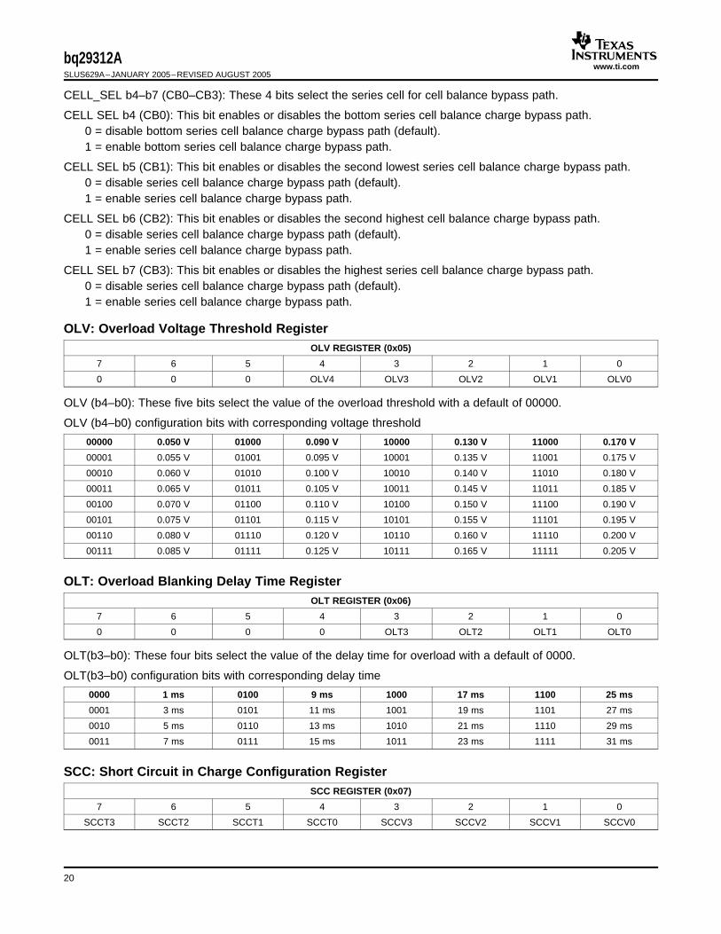
bq29312ASLUS629A–JANUARY 2005–REVISED AUGUST 2005
CELL_SEL b4–b7 (CB0–CB3): These 4 bits select the series cell for cell balance bypass path.
CELL SEL b4 (CB0): This bit enables or disables the bottom series cell balance charge bypass path.0 = disable bottom series cell balance charge bypass path (default).1 = enable bottom series cell balance charge bypass path.
CELL SEL b5 (CB1): This bit enables or disables the second lowest series cell balance charge bypass path.0 = disable series cell balance charge bypass path (default).1 = enable series cell balance charge bypass path.
CELL SEL b6 (CB2): This bit enables or disables the second highest cell balance charge bypass path.0 = disable series cell balance charge bypass path (default).1 = enable series cell balance charge bypass path.
CELL SEL b7 (CB3): This bit enables or disables the highest series cell balance charge bypass path.0 = disable series cell balance charge bypass path (default).1 = enable series cell balance charge bypass path.
OLV REGISTER (0x05)
7 6 5 4 3 2 1 0
0 0 0 OLV4 OLV3 OLV2 OLV1 OLV0
OLV (b4–b0): These five bits select the value of the overload threshold with a default of 00000.
OLV (b4–b0) configuration bits with corresponding voltage threshold
00000 0.050 V 01000 0.090 V 10000 0.130 V 11000 0.170 V
00001 0.055 V 01001 0.095 V 10001 0.135 V 11001 0.175 V
00010 0.060 V 01010 0.100 V 10010 0.140 V 11010 0.180 V
00011 0.065 V 01011 0.105 V 10011 0.145 V 11011 0.185 V
00100 0.070 V 01100 0.110 V 10100 0.150 V 11100 0.190 V
00101 0.075 V 01101 0.115 V 10101 0.155 V 11101 0.195 V
00110 0.080 V 01110 0.120 V 10110 0.160 V 11110 0.200 V
00111 0.085 V 01111 0.125 V 10111 0.165 V 11111 0.205 V
OLT REGISTER (0x06)
7 6 5 4 3 2 1 0
0 0 0 0 OLT3 OLT2 OLT1 OLT0
OLT(b3–b0): These four bits select the value of the delay time for overload with a default of 0000.
OLT(b3–b0) configuration bits with corresponding delay time
0000 1 ms 0100 9 ms 1000 17 ms 1100 25 ms
0001 3 ms 0101 11 ms 1001 19 ms 1101 27 ms
0010 5 ms 0110 13 ms 1010 21 ms 1110 29 ms
0011 7 ms 0111 15 ms 1011 23 ms 1111 31 ms
SCC REGISTER (0x07)
7 6 5 4 3 2 1 0
SCCT3 SCCT2 SCCT1 SCCT0 SCCV3 SCCV2 SCCV1 SCCV0
20
www.ti.com
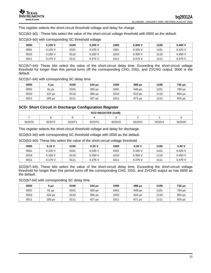
SCD: Short Circuit in Discharge Configuration Register
bq29312ASLUS629A–JANUARY 2005–REVISED AUGUST 2005
This register selects the short-circuit threshold voltage and delay for charge.
SCC(b3–b0) : These bits select the value of the short-circuit voltage threshold with 0000 as the default.
SCC(b3–b0) with corresponding SC threshold voltage
0000 0.100 V 0100 0.200 V 1000 0.300 V 1100 0.400 V
0001 0.125 V 0101 0.225 V 1001 0.325 V 1101 0.425 V
0010 0.150 V 0110 0.250 V 1010 0.350 V 1110 0.450 V
0011 0.175 V 0111 0.275 V 1011 0.375 V 1111 0.475 V
SCC(b7–b4): These bits select the value of the short-circuit delay time. Exceeding the short-circuit voltagethreshold for longer than this period turns off the corresponding CHG, DSG, and ZVCHG output. 0000 is thedefault.
SCC(b7–b4) with corresponding SC delay time
0000 0 µs 0100 244 µs 1000 488 µs 1100 732 µs
0001 61 µs 0101 305 µs 1001 549 µs 1101 793 µs
0010 122 µs 0110 366 µs 1010 610 µs 1110 854 µs
0011 183 µs 0111 427 µs 1011 671 µs 1111 915 µs
SCD REGISTER (0x08)
7 6 5 4 3 2 1 0
SCDT3 SCDT2 SCDT1 SCDT0 SCDV3 SCDV2 SCDV1 SCDV0
This register selects the short-circuit threshold voltage and delay for discharge.
SCD(b3–b0) with corresponding SC threshold voltage with 0000 as the default.
SCD(b3–b0): These bits select the value of the short-circuit voltage threshold
0000 0.10 V 0100 0.20 V 1000 0.30 V 1100 0.40 V
0001 0.125 V 0101 0.225 V 1001 0.325 V 1101 0.425 V
0010 0.150 V 0110 0.250 V 1010 0.350 V 1110 0.450 V
0011 0.175 V 0111 0.275 V 1011 0.375 V 1111 0.475 V
SCD(b7–b4): These bits select the value of the short-circuit delay time. Exceeding the short-circuit voltagethreshold for longer than this period turns off the corresponding CHG, DSG, and ZVCHG output as has 0000 asthe default.
SCD(b7-b4) with corresponding SC delay time
0000 0 µs 0100 244 µs 1000 488 µs 1100 732 µs
0001 61 µs 0101 305 µs 1001 549 µs 1101 793 µs
0010 122 µs 0110 366 µs 1010 610 µs 1110 854 µs
0011 183 µs 0111 427 µs 1011 671 µs 1111 915 µs
21

www.ti.com
APPLICATION INFORMATION
Precharge and 0-V Charging—Theory of Operation
0-V Charge FET Mode
PACK
ZVCHG
PMSREG
CHGDSG
BAT
ZVCHG-FETR(ZVCHG)
4.7 mF
Battery
DSG-FET CHG-FET Pack+
IZVCHG
IFASTCHG
CV
CC
Charger
DC Input
bq29312A
I(ZVCHG) = 0 V Precharge Current
I(FASTCHG) = Fast Current
OD
NC
bq29312ASLUS629A–JANUARY 2005–REVISED AUGUST 2005
In order to charge, the charge FET (CHG-FET) must be turned on to create a current path. When the V(BAT) is 0V and CHG-FET = ON, the V(PACK) is as low as the battery voltage. In this case, the supply voltage for the deviceis too low to operate. There are three possible configurations for this function and the bq29312A can be easilyconfigured according to the application needs. The three modes are 0-V Charge FET Mode, Common FETMode, and Precharge FET Mode.1. 0-V Charge FET Mode – Dedicates a precharge current path using an additional FET (ZVCHG-FET) to
sustain the PACK+ voltage level. The host charger is expected to provide a precharge function.2. Common FET Mode – Does not use a dedicated precharge FET. The charge FET (CHG-FET) is assured to
be set to ON state as default. The charger is expected to provide a precharge function.3. Precharge FET Mode – Dedicates a precharge current path using an additional open-drain (OD) pin drive
FET (PCHG-FET) FET to sustain the PACK+ voltage level. The charger does not provide any prechargefunction.
In this mode, a dedicated precharge current path using an additional FET (ZVCHG-FET) is required to sustain asuitable PACK+ voltage level. The charger is expected to provide the precharge function in this mode where theprecharge current level is suitable to charge cells below a set level, typically below 3 V per cell. When the lowestcell voltage rises above this level, then a fast charging current is applied by the charger.
The circuit diagram for this method is shown in Figure 7, showing how the additional FET is added in parallelwith the charge FET (CHG-FET).
Figure 7. 0-V Charge FET Mode Circuit
22

www.ti.com
VDS
PrechargeCurrent
ID
VGS
Point APoint B
bq29312ASLUS629A–JANUARY 2005–REVISED AUGUST 2005
APPLICATION INFORMATION (continued)
In order to pass 0 V or precharge current, an appropriate gate-source voltage V(GS), for ZVCHG-FET must beapplied. Here, V(PACK) can be expressed in terms of V(GS) as follows:
V(PACK) = V(ZVCHG) + V(GS) (ZVCHG-FET gate - source voltage)
Figure 8. Drain Current vs Drain-Source Voltage Characteristics
In the bq29312A, the initial state is for CHG-FET = OFF and ZVCHG-FET = ON with the V(ZVCHG) clamped at 3.5V initially. Then, the charger applies a constant current and raises V(PACK) high enough to pass the prechargecurrent, point A. For example, if the V(GS) is 2 V at this point, V(PACK) is 3.5 V + 2 V = 5.5 V. Also, theZVCHG-FET is used in its MOS saturation region at this point so that V(DS) is expressed as follows:
V(PACK) = V(BAT) + VF + VDS(ZVCHG-FET)
where V(F) = 0.7 V is the forward voltage of a DSG-FET back diode and is typically 0.7 V.
This derives the following equation:VDS = 4.8 V - V(BAT)
As the battery is charged V(BAT) increases and the V(DS) voltage decreases reaching its linear region. Forexample: If the linear region is 0.2 V, this state continues until V(BAT) = 4.6 V, (4.8 V - 0.2 V).
As V(BAT) increases further, V(PACK) and the V(GS) voltage increase. But the VDS remains at 0.2 V because theZVCHG-FET is driven in its MOS linear region, point B.
V(PACK) = VF + 0.2 V + V(BAT)
where VF = 0.7 V is the forward voltage of a DSG-FET back diode and is typically 0.7 V
The R(ZVCHG) purpose is to split heat dissipation across the ZVCHG-FET and the resistor.
ZVCHG pin behavior is shown in Figure 9 where V(ZVCHG) is set to 0 V at the beginning.
23

www.ti.com
t - Time - mS
Vo
ltag
e - V
0 4 8 12 16
4
20
10
0
8
2
6
14
18
12
16
20
V(PACK)
3.5 V
V(ZVCHG)=V(PACK) - 8 V
V(ZVCHG)= V(PACK) / 2
V(BAT)
bq29312ASLUS629A–JANUARY 2005–REVISED AUGUST 2005
APPLICATION INFORMATION (continued)
Figure 9. Voltage Transition at ZVCHG, PACK, and BAT
As V(PACK) exceeds 7 V, V(ZVCHG) = V(PACK)/2. However, V(ZVCHG) is maintained to limit the voltage between PACKand ZVCHG at a maximum of 8 V(typ). This limitation is intended to avoid excessive voltage between the gateand the source of ZVCHG-FET.
The signal timing is shown in Figure 10. When precharge begins, (V(BAT) = 0 V) V(PACK) is clamped to 3.5 V andholds the supply voltage for bq29312A operation. After V(BAT) reaches sufficient voltage high enough forbq29312A operation, the CHG-FET and the DSG-FET are turned ON and ZVCHG-FET is turned OFF.
Although the current path is changed, the same precharging current is still applied. When V(BAT) reaches the fastcharging voltage (typical 3 V per cell), the charger switches into fast charging mode.
24

www.ti.com
ONZVCHG FET = OFF
OFF CHG FET = ON
OFF CHG FET = ON
3.5 V+VGS(ZVCHGFET)0 V
3.3 V0 V
V = VPACK*(1/2)
3.5 V (typ.)0 V
”L” (1 V)
”L” (1 V)
0 V
Fast Charge Current
0 V and Precharge Current0 A
0 V Charge Mode Precharge
Mode
Fast Charge Mode
V(PACK)
REG
ZVCHG
GHD
DSG
BatteryVoltage
ChargeCurrent
Common FET
bq29312ASLUS629A–JANUARY 2005–REVISED AUGUST 2005
APPLICATION INFORMATION (continued)
Figure 10. Signal Timing of Pins During 0-V Charging and Precharging (0-V Charge FET)
This mode does not require a dedicated precharge FET (ZVCHG-FET). The charge FET (CHG-FET) is ON atinitialization of the bq29312A when PMS = V(PACK), allowing for 0 V or precharge current to flow. The applicationcircuit is shown in Figure 11. The charger is expected to provide the precharge function in this mode, where thecharger provides a precharge current level suitable to charge cells below a set level, typically below 3 V per cell.When the lowest cell voltage rises above this level, then a fast charging current is applied.
When the charger is connected, the voltage at PMS rises. Once it is above 0.7 V, the CHG output is driven toGND which turns ON the CHG-FET. The charging current flows through the CHG-FET and a back diode ofDSG-FET. The pack voltage is represented by the following equation.
V(PACK) = V(BAT) + VF + VDS(CHG-FET)
Where VF = 0.7 V is the forward voltage of a DSG-FET back diode and is typically 0.7 V.
While V(PACK) is maintained above 0.7 V, the precharging current is maintained. While V(PACK) and V(BAT) areunder the bq29312A supply voltage, then the bq29312A regulator is inactive and the host controller is notfunctional. Thus, any protection features of this chipset do not function during this period. This state continuesuntil V(PACK) goes higher than the bq29312A minimum supply voltage.
When V(BAT) rises and V(PACK) reaches bq29312A minimum supply voltage, the REG output is active providing a3.3-V (typ) supply to the host. When this level is reached, the CHG pin changes its state from GND to the levelcontrolled with CHG bit in bq29312A registers. In this state, the CHG output level is driven by a clamp circuit sothat its voltage level changes from 0 V to 1 V. Also, the host controller is active and can turn ON the DSG-FET.
25

www.ti.com
PACK
ZVCHG
PMSREG
CHGDSG
BAT
4.7 mF
Battery
DSG-FET CHG-FET Pack+
I(ZVCHG)
I(FASTCHG)
CV
CC
Charger
DC Input
bq29312A
I(ZVCHG) = 0 V Precharge Current
I(FASTCHG) = Fast Current
OD
NC
bq29312ASLUS629A–JANUARY 2005–REVISED AUGUST 2005
APPLICATION INFORMATION (continued)
The disadvantages is that during 0-V charging, bq29312A is inactive. The device does not protect the batteryand does not update battery information (now is 0 V charging) to the PC.
There are two advantage of this configuration:1. The voltage between BAT and PACK is lower. Higher precharge current is allowed due to less heat loss in
the FET, and no external resistor is required.2. The charge FET is turned on during precharging. The precharge current can be fully controlled by the
charger.
Figure 11. Common FET Mode Circuit Diagram
The signal timing during the common FET mode is shown in Figure 12. The CHG-FET is turned on when thecharger is connected. As V(BAT) rises and V(PACK) reaches the bq29312A minimum supply voltage, the REGoutput becomes active and the host controller starts to work.
When V(PACK) becomes high enough, the host controller turns ON the DSG-FET. The charger enters the fastcharging mode when V(BAT) reaches the fast charge level.
26
www.ti.com
0 V Precharge Mode Fast Charge Mode
V(PACK)
REG
PMS
CHG
DSG
BatteryVoltage
ChargeCurrent
Host =Inactive Host = Active
Set to ”L” asPMS = PACK Set to ”L” by Host
Host SetsDSG-FET to ON
0.7 V0 V
3.3 V
0 V
0 V
”L” (1 V)0 V
”L” (1 V)
0 V
Fast Charge Current
0 V and Precharge Current0 A
Precharge FET
bq29312ASLUS629A–JANUARY 2005–REVISED AUGUST 2005
APPLICATION INFORMATION (continued)
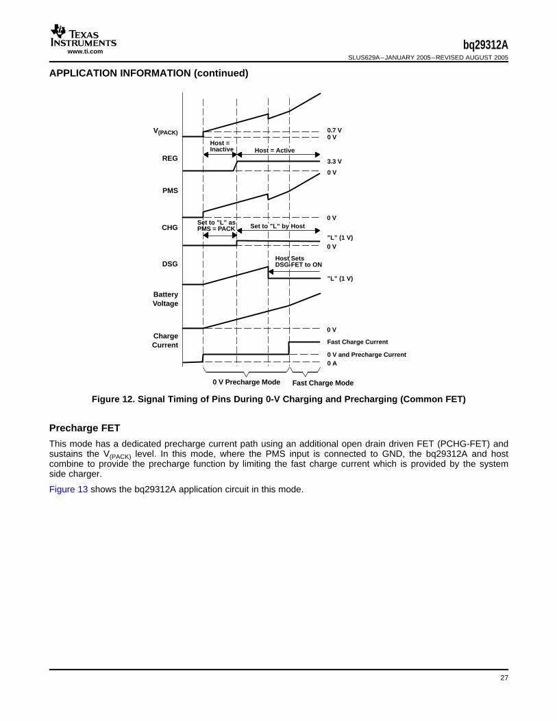
Figure 12. Signal Timing of Pins During 0-V Charging and Precharging (Common FET)
This mode has a dedicated precharge current path using an additional open drain driven FET (PCHG-FET) andsustains the V(PACK) level. In this mode, where the PMS input is connected to GND, the bq29312A and hostcombine to provide the precharge function by limiting the fast charge current which is provided by the systemside charger.
Figure 13 shows the bq29312A application circuit in this mode.
27

www.ti.com
PACK
ZVCHG
PMS
REG
CHGDSG
BAT
PCHG-FETR(PCHG)
4.7 mF
Battery
DSG-FET CHG-FET Pack+
I(FASTCHG)
CV
CC
Charger
DC Input
bq29312A
I(FASTCHG) = Fast Current
OD
Host
SCLK SDATA
ID
VSD
ID = (V(PACK) - V(BAT) - VDS)/R(PCHG)
bq29312ASLUS629A–JANUARY 2005–REVISED AUGUST 2005
APPLICATION INFORMATION (continued)
Figure 13. Precharge FET Mode Circuit Diagram
The PCHG-FET is driven by the OD output, and the resister R(PCHG) in the precharge path limits the prechargecurrent. When OD = GND, then the PCHG-FET is ON. The precharge current is represented by the followingequation:
I(PCHG) = ID = ( V(PACK) - V(BAT) - VDS )/R(PCHG)
• A load curve of the PCHG-FET is shown in Figure 14. When the drain-source voltage (VDS) is high enough,the PCHG-FET operates in the linear region and has low resistance. By approximating VDS as 0 V, theprecharge current, I(PCHG) is expressed as below.
• I(PCHG) = ( V(PACK) - V(BAT) )/R(PCHG)
Figure 14. PCHG-FET ID—VDS Characteristic
During the precharge phase, CHG-FET is turned OFF and PCHG-FET is turned ON. When all the cell voltagesmeasured by the host reach the fast charge threshold, the host controller turns ON CHG-FET and turns OFFPCHG-FET. The signal timing is shown in Figure 15.
When the charger is connected, CHG-FET, DSG-FET and PCHG-FET are already in the OFF state. When thecharger in connected, it applies V(PACK). The bq29312A REG output then becomes active and supplies power tothe host controller. As the host controller starts up, it turns on the OD pin and the precharge current is enabled.
28

www.ti.com
Charge CV
0 V
Host : Active
3.3 V
0 V
OFF
CHG FET = OFF
OFF
0 V
DSG FET = ON
”L” (1 V)
OFF ”L” (1 V)
0 VFast Charge Current
0 V and Precharge Current0 A
0 V and Precharge Mode
Fast ChargeMode
V(PACK)
REG
CHG
DSG
BatteryVoltage
ChargeCurrent Charge
Charge Mode
OD PCHG FET = ON
bq29312ASLUS629A–JANUARY 2005–REVISED AUGUST 2005
APPLICATION INFORMATION (continued)
In this configuration, attention must be paid to high power consumption in the PCHG-FET and the series resistorR(PCHG). The highest power is consumed when VBAT = 0 V, where it is the highest differential between the PACKand BAT pins. For example, the power consumption in 4-series cells with 17.4 V fast charge voltage and R(PCHG)= 188 Ω is expressed below.• IPCHG = (17.4 V – 0.0 V)/188 Ω = 92.6 mA• 17.4 V × 92.6 mA = 1.61 W
An optional solution is to combine a thermistor with a resistor to create R(PCHG); therefore, as temperatureincreases, the current reduces.
Once the lowest cell voltage reaches the fast charge level (typ 3.0 V per cell), the host controller turns ONCHG-FET and DSG-FET, and turns OFF PCHG-FET.
It is also appropriate to turn on DSG-FET during precharge in order to supply precharge current efficiently, asshown in Figure 15.
Figure 15. Signal Timing of Pins During 0-V Charging and Precharging (Precharge FET)
29

www.ti.com
Summary
bq29312ASLUS629A–JANUARY 2005–REVISED AUGUST 2005
APPLICATION INFORMATION (continued)
The three types of 0-V charge options available with the bq29312A are summarized in Table 4.
Table 4. Charge Options
CHARGE MODE TYPE HOST CHARGE CAPABILITIES KEY APPLICATION CIRCUIT NOTES
PMS = GND
1) 0-V Charge FET Fast charge and precharge ZVCHG: Drives 0-V charge FET (ZVCHG-FET)
OD: Not used
PMS = PACK
2) Common FET Fast charge and precharge ZVCHG: Not used
OD: Not used
PMS = GND
3) Precharge FET Fast charge but no precharge function ZVCHG: Not used
OD: Drives the precharge FET (PCHG-FET)
There a number of tradeoffs between the various 0-V charge modes which are discussed as follows:• 0-V Charge FET (1) vs Common FET (2)
When the charger has both precharge and charging functions, two types of circuit configuration are available.1. 0-V Charge FET – The bq29312A is active even during precharge. Therefore, the host can update the
battery status to the system and protect the battery pack by detecting abnormal conditions.– A high voltage is applied on the 0-V charge FET at 0-V cell voltage. In order to avoid excessive heat
generation, the 0-V charge current must be limited.2. Common FET – During 0-V charge the bq29312A and the host are not active. Therefore, they cannot protect
the cells and cannot update the battery status to the system.– The bq29312A can tolerate high 0-V charge current as heat generation is not excessive.– A dedicated FET for the 0-V charge is not required.
• 0-V Charge FET (1) vs Precharge FET (3)
The current paths of the 0-V charge FET (1) and Precharge FET (3) modes are the same. If the 0-V charge FET(1) mode is used with chargers without precharge function, the bq29312A consumes extra current of up to 1 mAin order to turn ON the ZVCHG output.1. If the charger has a precharge function, ZVCHG-FET is turned ON only during 0-V charging. In this case, a
1-mA increase is not a concern because the charger is connected during the 0-V charging period.2. If the charger does not have precharge function, the ZVCHG-FET must be turned ON during 0-V charging
and also precharging. When the battery reaches an overdischarged state, it must turn OFF DSG-FET andCHG-FET and turn ON ZVCHG-FET. The reason for this is the battery must keep the 0-V charge path whilewaiting for a charger to be connected to limit the current.– Consuming 1 mA, while waiting for a charger to be connected in overdischarge state, is significant if
compared to current consumption of other modes.• Precharge FET (3)
If the precharge FET (3) mode is used with a charger with precharge function, care must be taken as limiting the0-V charge current with resistance may cause some issues. The charger may start fast charge immediately, ordetect an abnormal condition.
When the charger is connected, the charger may raise the output voltage to force the precharge current. In orderto ensure a supply voltage for the bq29312A during 0-V charging, the resistance of a series resister (RPCHG) mustbe high enough. This may result in a high VPACK, and some chargers may detect it as an abnormal condition.
30

PACKAGE OPTION ADDENDUM
www.ti.com 1-Dec-2015
Addendum-Page 1
PACKAGING INFORMATION
Orderable Device Status(1)
Package Type PackageDrawing
Pins PackageQty
Eco Plan(2)
Lead/Ball Finish(6)
MSL Peak Temp(3)
Op Temp (°C) Device Marking(4/5)
Samples
BQ29312APW NRND TSSOP PW 24 60 Green (RoHS& no Sb/Br)
CU NIPDAU Level-1-260C-UNLIM -40 to 85 29312APW
BQ29312APWG4 NRND TSSOP PW 24 60 Green (RoHS& no Sb/Br)
CU NIPDAU Level-1-260C-UNLIM -40 to 85 29312APW
BQ29312APWR NRND TSSOP PW 24 2000 Green (RoHS& no Sb/Br)
CU NIPDAU Level-1-260C-UNLIM -40 to 85 29312APW
BQ29312APWRG4 NRND TSSOP PW 24 2000 Green (RoHS& no Sb/Br)
CU NIPDAU Level-1-260C-UNLIM -40 to 85 29312APW
BQ29312ARTHR NRND VQFN RTH 24 3000 Green (RoHS& no Sb/Br)
CU NIPDAUAG Level-2-260C-1 YEAR -40 to 85 29312A
BQ29312ARTHRG4 NRND VQFN RTH 24 3000 Green (RoHS& no Sb/Br)
CU NIPDAUAG Level-2-260C-1 YEAR -40 to 85 29312A
(1) The marketing status values are defined as follows:ACTIVE: Product device recommended for new designs.LIFEBUY: TI has announced that the device will be discontinued, and a lifetime-buy period is in effect.NRND: Not recommended for new designs. Device is in production to support existing customers, but TI does not recommend using this part in a new design.PREVIEW: Device has been announced but is not in production. Samples may or may not be available.OBSOLETE: TI has discontinued the production of the device.
(2) Eco Plan - The planned eco-friendly classification: Pb-Free (RoHS), Pb-Free (RoHS Exempt), or Green (RoHS & no Sb/Br) - please check http://www.ti.com/productcontent for the latest availabilityinformation and additional product content details.TBD: The Pb-Free/Green conversion plan has not been defined.Pb-Free (RoHS): TI's terms "Lead-Free" or "Pb-Free" mean semiconductor products that are compatible with the current RoHS requirements for all 6 substances, including the requirement thatlead not exceed 0.1% by weight in homogeneous materials. Where designed to be soldered at high temperatures, TI Pb-Free products are suitable for use in specified lead-free processes.Pb-Free (RoHS Exempt): This component has a RoHS exemption for either 1) lead-based flip-chip solder bumps used between the die and package, or 2) lead-based die adhesive used betweenthe die and leadframe. The component is otherwise considered Pb-Free (RoHS compatible) as defined above.Green (RoHS & no Sb/Br): TI defines "Green" to mean Pb-Free (RoHS compatible), and free of Bromine (Br) and Antimony (Sb) based flame retardants (Br or Sb do not exceed 0.1% by weightin homogeneous material)
(3) MSL, Peak Temp. - The Moisture Sensitivity Level rating according to the JEDEC industry standard classifications, and peak solder temperature.
(4) There may be additional marking, which relates to the logo, the lot trace code information, or the environmental category on the device.
(5) Multiple Device Markings will be inside parentheses. Only one Device Marking contained in parentheses and separated by a "~" will appear on a device. If a line is indented then it is a continuationof the previous line and the two combined represent the entire Device Marking for that device.

PACKAGE OPTION ADDENDUM
www.ti.com 1-Dec-2015
Addendum-Page 2
(6) Lead/Ball Finish - Orderable Devices may have multiple material finish options. Finish options are separated by a vertical ruled line. Lead/Ball Finish values may wrap to two lines if the finishvalue exceeds the maximum column width.
Important Information and Disclaimer:The information provided on this page represents TI's knowledge and belief as of the date that it is provided. TI bases its knowledge and belief on informationprovided by third parties, and makes no representation or warranty as to the accuracy of such information. Efforts are underway to better integrate information from third parties. TI has taken andcontinues to take reasonable steps to provide representative and accurate information but may not have conducted destructive testing or chemical analysis on incoming materials and chemicals.TI and TI suppliers consider certain information to be proprietary, and thus CAS numbers and other limited information may not be available for release.
In no event shall TI's liability arising out of such information exceed the total purchase price of the TI part(s) at issue in this document sold by TI to Customer on an annual basis.

TAPE AND REEL INFORMATION
*All dimensions are nominal
Device PackageType
PackageDrawing
Pins SPQ ReelDiameter
(mm)
ReelWidth
W1 (mm)
A0(mm)
B0(mm)
K0(mm)
P1(mm)
W(mm)
Pin1Quadrant
BQ29312APWR TSSOP PW 24 2000 330.0 16.4 6.95 8.3 1.6 8.0 16.0 Q1
BQ29312ARTHR VQFN RTH 24 3000 330.0 12.4 4.25 4.25 1.15 8.0 12.0 Q2
PACKAGE MATERIALS INFORMATION
www.ti.com 14-Jul-2012
Pack Materials-Page 1

*All dimensions are nominal
Device Package Type Package Drawing Pins SPQ Length (mm) Width (mm) Height (mm)
BQ29312APWR TSSOP PW 24 2000 367.0 367.0 38.0
BQ29312ARTHR VQFN RTH 24 3000 367.0 367.0 35.0
PACKAGE MATERIALS INFORMATION
www.ti.com 14-Jul-2012
Pack Materials-Page 2


IMPORTANT NOTICE
Texas Instruments Incorporated and its subsidiaries (TI) reserve the right to make corrections, enhancements, improvements and otherchanges to its semiconductor products and services per JESD46, latest issue, and to discontinue any product or service per JESD48, latestissue. Buyers should obtain the latest relevant information before placing orders and should verify that such information is current andcomplete. All semiconductor products (also referred to herein as “components”) are sold subject to TI’s terms and conditions of salesupplied at the time of order acknowledgment.TI warrants performance of its components to the specifications applicable at the time of sale, in accordance with the warranty in TI’s termsand conditions of sale of semiconductor products. Testing and other quality control techniques are used to the extent TI deems necessaryto support this warranty. Except where mandated by applicable law, testing of all parameters of each component is not necessarilyperformed.TI assumes no liability for applications assistance or the design of Buyers’ products. Buyers are responsible for their products andapplications using TI components. To minimize the risks associated with Buyers’ products and applications, Buyers should provideadequate design and operating safeguards.TI does not warrant or represent that any license, either express or implied, is granted under any patent right, copyright, mask work right, orother intellectual property right relating to any combination, machine, or process in which TI components or services are used. Informationpublished by TI regarding third-party products or services does not constitute a license to use such products or services or a warranty orendorsement thereof. Use of such information may require a license from a third party under the patents or other intellectual property of thethird party, or a license from TI under the patents or other intellectual property of TI.Reproduction of significant portions of TI information in TI data books or data sheets is permissible only if reproduction is without alterationand is accompanied by all associated warranties, conditions, limitations, and notices. TI is not responsible or liable for such altereddocumentation. Information of third parties may be subject to additional restrictions.Resale of TI components or services with statements different from or beyond the parameters stated by TI for that component or servicevoids all express and any implied warranties for the associated TI component or service and is an unfair and deceptive business practice.TI is not responsible or liable for any such statements.Buyer acknowledges and agrees that it is solely responsible for compliance with all legal, regulatory and safety-related requirementsconcerning its products, and any use of TI components in its applications, notwithstanding any applications-related information or supportthat may be provided by TI. Buyer represents and agrees that it has all the necessary expertise to create and implement safeguards whichanticipate dangerous consequences of failures, monitor failures and their consequences, lessen the likelihood of failures that might causeharm and take appropriate remedial actions. Buyer will fully indemnify TI and its representatives against any damages arising out of the useof any TI components in safety-critical applications.In some cases, TI components may be promoted specifically to facilitate safety-related applications. With such components, TI’s goal is tohelp enable customers to design and create their own end-product solutions that meet applicable functional safety standards andrequirements. Nonetheless, such components are subject to these terms.No TI components are authorized for use in FDA Class III (or similar life-critical medical equipment) unless authorized officers of the partieshave executed a special agreement specifically governing such use.Only those TI components which TI has specifically designated as military grade or “enhanced plastic” are designed and intended for use inmilitary/aerospace applications or environments. Buyer acknowledges and agrees that any military or aerospace use of TI componentswhich have not been so designated is solely at the Buyer's risk, and that Buyer is solely responsible for compliance with all legal andregulatory requirements in connection with such use.TI has specifically designated certain components as meeting ISO/TS16949 requirements, mainly for automotive use. In any case of use ofnon-designated products, TI will not be responsible for any failure to meet ISO/TS16949.
Products ApplicationsAudio www.ti.com/audio Automotive and Transportation www.ti.com/automotiveAmplifiers amplifier.ti.com Communications and Telecom www.ti.com/communicationsData Converters dataconverter.ti.com Computers and Peripherals www.ti.com/computersDLP® Products www.dlp.com Consumer Electronics www.ti.com/consumer-appsDSP dsp.ti.com Energy and Lighting www.ti.com/energyClocks and Timers www.ti.com/clocks Industrial www.ti.com/industrialInterface interface.ti.com Medical www.ti.com/medicalLogic logic.ti.com Security www.ti.com/securityPower Mgmt power.ti.com Space, Avionics and Defense www.ti.com/space-avionics-defenseMicrocontrollers microcontroller.ti.com Video and Imaging www.ti.com/videoRFID www.ti-rfid.comOMAP Applications Processors www.ti.com/omap TI E2E Community e2e.ti.comWireless Connectivity www.ti.com/wirelessconnectivity
Mailing Address: Texas Instruments, Post Office Box 655303, Dallas, Texas 75265Copyright © 2015, Texas Instruments Incorporated


![Research Article Analysis of Leakage Reduction Techniques ...Chinese Journalof Engineering cell data stability is acquired by lowering supply voltage and threshold voltages [ ]. erefore](https://static.fdocuments.us/doc/165x107/60fb6aafb691637d81252863/research-article-analysis-of-leakage-reduction-techniques-chinese-journalof.jpg)