Tutorial Outline - College of Engineering | UMass Amherst · ISCA Tutorial: Low Power Design...
28
1 Memories.1 ISCA Tutorial: Low Power Design ©MJI&VN, PSU, 2000 Tutorial Outline Introduction and motivation Sources of power in CMOS designs Power analysis tools and techniques Gate & functional unit design issues & techniques BREAK Architectural level issues and techniques LUNCH Low power memory system design Software level issues and techniques BREAK Software level issues and techniques, con’t Future challenges 8:30 - 8:45 8:45 - 9:05 9:05 - 9:30 9:30 - 10:30 10:30 - 10:50 10:50 - 12:15 12:15 - 1:30 1:30 - 2:30 2:30 - 3:30 3:30 - 3:50 3:50 - 4:30 4:30 - 4:45 Memories.2 ISCA Tutorial: Low Power Design ©MJI&VN, PSU, 2000 Typical Memory Hierarchy Control Datapath Secondary Storage (Disk) On-Chip Components RegFile Main Memory (DRAM) Second Level Cache (SRAM) Data Cache Instr Cache ITLB DTLB DEC 21164a (2.0V dd , 0.35μ, 400MHz, 30W max) –caches dissipate 25% of the total chip power DEC SA-110 (2.0V dd , 0.35μ, 233MHz, 1W typ) – no L2 on-chip –I$ (D$) dissipate 27% (16%) of the total chip power eDRAM
Transcript of Tutorial Outline - College of Engineering | UMass Amherst · ISCA Tutorial: Low Power Design...

1
Memories.1ISCA Tutorial: Low Power Design ©MJI&VN, PSU, 2000
Tutorial OutlineIntroduction and motivationSources of power in CMOS designsPower analysis tools and techniquesGate & functional unit design issues & techniquesBREAKArchitectural level issues and techniquesLUNCHLow power memory system designSoftware level issues and techniquesBREAKSoftware level issues and techniques, con’tFuture challenges
8:30 - 8:45 8:45 - 9:05 9:05 - 9:30 9:30 - 10:3010:30 - 10:5010:50 - 12:1512:15 - 1:30 1:30 - 2:30 2:30 - 3:30 3:30 - 3:50 3:50 - 4:30 4:30 - 4:45
Memories.2ISCA Tutorial: Low Power Design ©MJI&VN, PSU, 2000
Typical Memory Hierarchy
Control
Datapath
SecondaryStorage(Disk)
On-Chip Components
RegF
ile
MainMemory(DRAM)
SecondLevelCache
(SRAM)
Data
Cache
InstrC
ache
ITLB
DT
LB
DEC 21164a (2.0Vdd, 0.35µ, 400MHz, 30W max)
–caches dissipate 25% of the total chip power
DEC SA-110 (2.0Vdd, 0.35µ, 233MHz, 1W typ) – no L2 on-chip
–I$ (D$) dissipate 27% (16%) of the total chip power
eDRAM
2
Memories.3ISCA Tutorial: Low Power Design ©MJI&VN, PSU, 2000
Importance of OptimizingMemory System Energy
● Many emerging applications are data-intensive
● For ASICs and embedded systems,memory system can contribute up to 90%energy
● Multiple memories in future System-on-chip designs
Memories.4ISCA Tutorial: Low Power Design ©MJI&VN, PSU, 2000
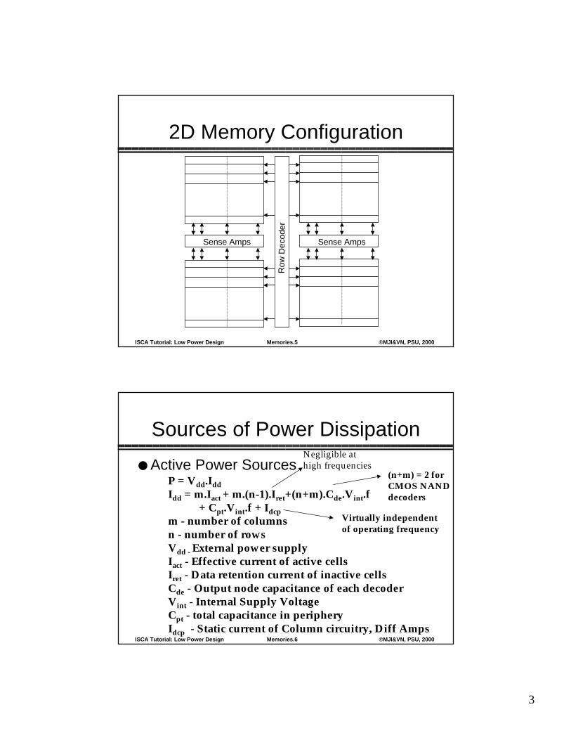
2D Memory Architecture
A0
Row
Dec
oder
A1
Aj-1
Sense Amplifiers
bit line
word line
storage(RAM) cell
Row
Add
ress
Col
umn
Add
ress
Aj
Aj+1
Ak-1
Read/Write Circuits
Column Decoder
2k-j
m2j
Input/Output (m bits)
amplifies bit line swing
selects appropriateword from memory row
3
Memories.5ISCA Tutorial: Low Power Design ©MJI&VN, PSU, 2000
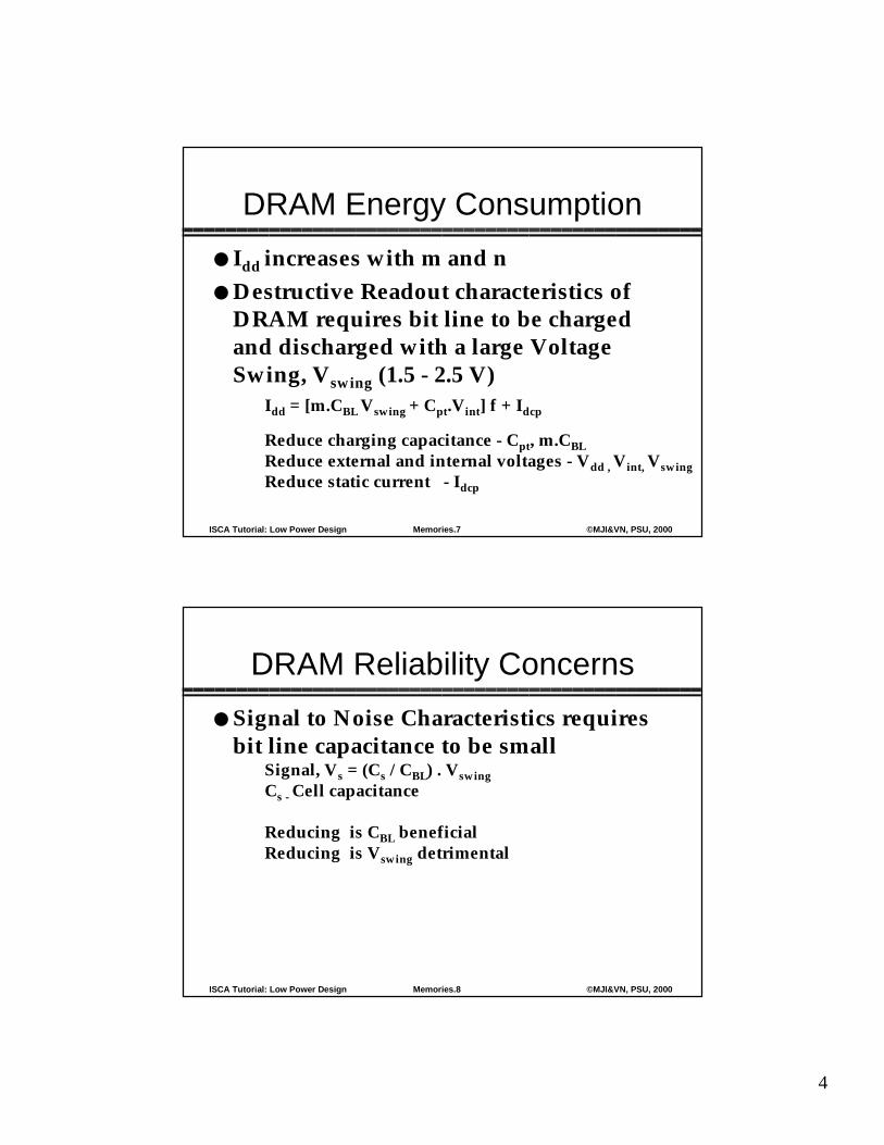
2D Memory Configuration
Row
Dec
oder
Sense AmpsSense Amps
Memories.6ISCA Tutorial: Low Power Design ©MJI&VN, PSU, 2000
Sources of Power Dissipation
● Active Power SourcesP = Vdd.IddIdd = m.Iact + m.(n-1).Iret+(n+m).Cde.Vint.f + Cpt.Vint.f + Idcpm - number of columnsn - number of rowsVdd - External power supplyIact - Effective current of active cellsIret - Data retention current of inactive cellsCde - Output node capacitance of each decoderVint - Internal Supply VoltageCpt - total capacitance in peripheryIdcp - Static current of Column circuitry, Diff Amps
(n+m) = 2 forCMOS NANDdecoders
Negligible athigh frequencies
Virtually independentof operating frequency
4
Memories.7ISCA Tutorial: Low Power Design ©MJI&VN, PSU, 2000
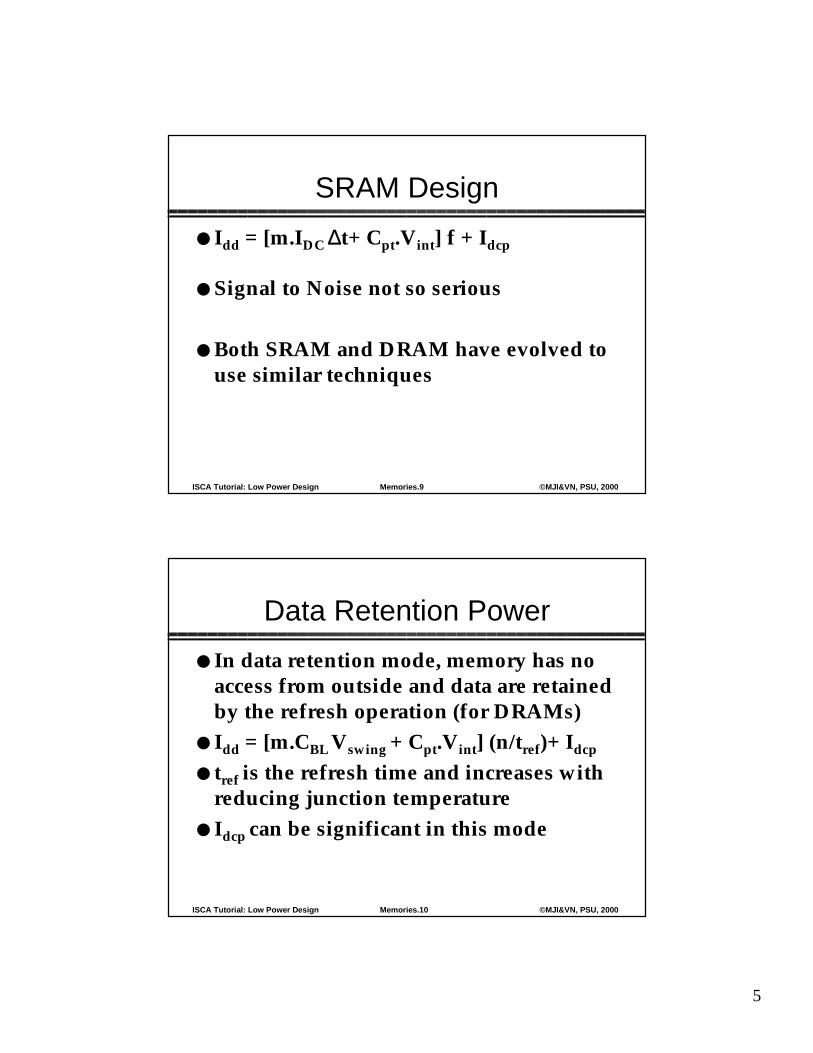
DRAM Energy Consumption
● Idd increases with m and n● Destructive Readout characteristics of
DRAM requires bit line to be chargedand discharged with a large VoltageSwing, Vswing (1.5 - 2.5 V)
Idd = [m.CBL Vswing + Cpt.Vint] f + Idcp
Reduce charging capacitance - Cpt, m.CBL Reduce external and internal voltages - Vdd , Vint, VswingReduce static current - Idcp
Memories.8ISCA Tutorial: Low Power Design ©MJI&VN, PSU, 2000
DRAM Reliability Concerns
● Signal to Noise Characteristics requiresbit line capacitance to be small
Signal, Vs = (Cs / CBL) . Vswing Cs - Cell capacitance
Reducing is CBL beneficialReducing is Vswing detrimental
5
Memories.9ISCA Tutorial: Low Power Design ©MJI&VN, PSU, 2000
SRAM Design
● Idd = [m.IDC ∆t+ Cpt.Vint] f + Idcp
● Signal to Noise not so serious
● Both SRAM and DRAM have evolved touse similar techniques
Memories.10ISCA Tutorial: Low Power Design ©MJI&VN, PSU, 2000
Data Retention Power
● In data retention mode, memory has noaccess from outside and data are retainedby the refresh operation (for DRAMs)
● Idd = [m.CBL Vswing + Cpt.Vint] (n/tref)+ Idcp
● tref is the refresh time and increases withreducing junction temperature
● Idcp can be significant in this mode

6
Memories.11ISCA Tutorial: Low Power Design ©MJI&VN, PSU, 2000
SRAM Power Budget
0
20
40
60
128x128 256x64 64x256
DecodersWord lineBL+SA+CellWrite cktRead ckt
Array Size
Ave
rage
mW
16K bits0.5µ technology10ns cycle time4.05ns access time3.3V Vdd
From Chang, 1997
Memories.12ISCA Tutorial: Low Power Design ©MJI&VN, PSU, 2000
Low Power SRAM Techniques
● Standby power reduction● Operating power reduction
» memory bank partitioning» SRAM cell design» reduced bit line swing (pulsed word line and
bit line isolation)» divided word line» bit line segmentation
● Can use the above in combination!

7
Memories.13ISCA Tutorial: Low Power Design ©MJI&VN, PSU, 2000
Memory Bank Partitioning● Partition the memory array into smaller
banks so that only the addressed bank isactivated» improves speed and lowers power» word line capacitance reduced» number of bit cells activated reduced
● At some point the delay and poweroverhead associated with the bank decodingcircuit dominates (2 to 8 banks typical)
Memories.14ISCA Tutorial: Low Power Design ©MJI&VN, PSU, 2000
Partitioned Memory Structure
Row
Add
rC
olum
nA
ddr
Blo
ckA
ddr
Input/Output (m bits)
Advantages: 1. Shorter word and/or bit lines 2. Block addr activates only 1 block saving power

8
Memories.15ISCA Tutorial: Low Power Design ©MJI&VN, PSU, 2000
SRAM Cell
● 6-T SRAMs cell reduces static current (leakage)but takes more area
● Reduction of Vth in very low Vdd SRAMs suffer from large leakage currents
» use multiple threshold devices (memory cells withhigher Vth to reduce leakage while peripheral circuitsuse low Vth to improve speed)
BL
WL
BL
Memories.16ISCA Tutorial: Low Power Design ©MJI&VN, PSU, 2000
Switched Power Supply withLevel Holding
● Multi Vt device by changing Well voltages;Vt high during standby & low otherwise
Q
High Vt1 - Normal0 - not used
Vdd
High Vt0 - Normal1 - Not used
Level Holder CircuitLow Vt

9
Memories.17ISCA Tutorial: Low Power Design ©MJI&VN, PSU, 2000
Reduced Bit Line Swing
● Limit voltage swing on bit lines to improveboth speed and power» need sense amp for each column to
sense/restore signal» isolate memory cells from the bit lines after
sensing (to prevent the cells from changingthe bit line voltage further) - pulsed word line
» isolate sense amps from bit lines after sensing(to prevent bit lines from having large voltageswings) - bit line isolation
Memories.18ISCA Tutorial: Low Power Design ©MJI&VN, PSU, 2000
Pulsed Word Line
● Generation of word line pulses very critical» too short - sense amp operation may fail» too long - power efficiency degraded
(because bit line swing size depends onduration of the word line pulse)
● Word line pulse generation» delay lines (susceptible to process, temp, etc.)» use feedback from bit lines

10
Memories.19ISCA Tutorial: Low Power Design ©MJI&VN, PSU, 2000
Pulsed Word Line Structure
● Dummy column» height set to 10% of a regular column and its
cells are tied to a fixed value» capacitance is only 10% of a regular column
Read Word line
Bit lines
Complete
Dummybit lines
10%populated
Memories.20ISCA Tutorial: Low Power Design ©MJI&VN, PSU, 2000
Pulsed Word Line Timing
● Dummy bit lines have reached full swingand trigger pulse shut off when regular bitlines reach 10% swing
Read
Complete
Word line
Bit line
Dummy bit line ∆V = Vdd
∆V = 0.1Vdd
11
Memories.21ISCA Tutorial: Low Power Design ©MJI&VN, PSU, 2000
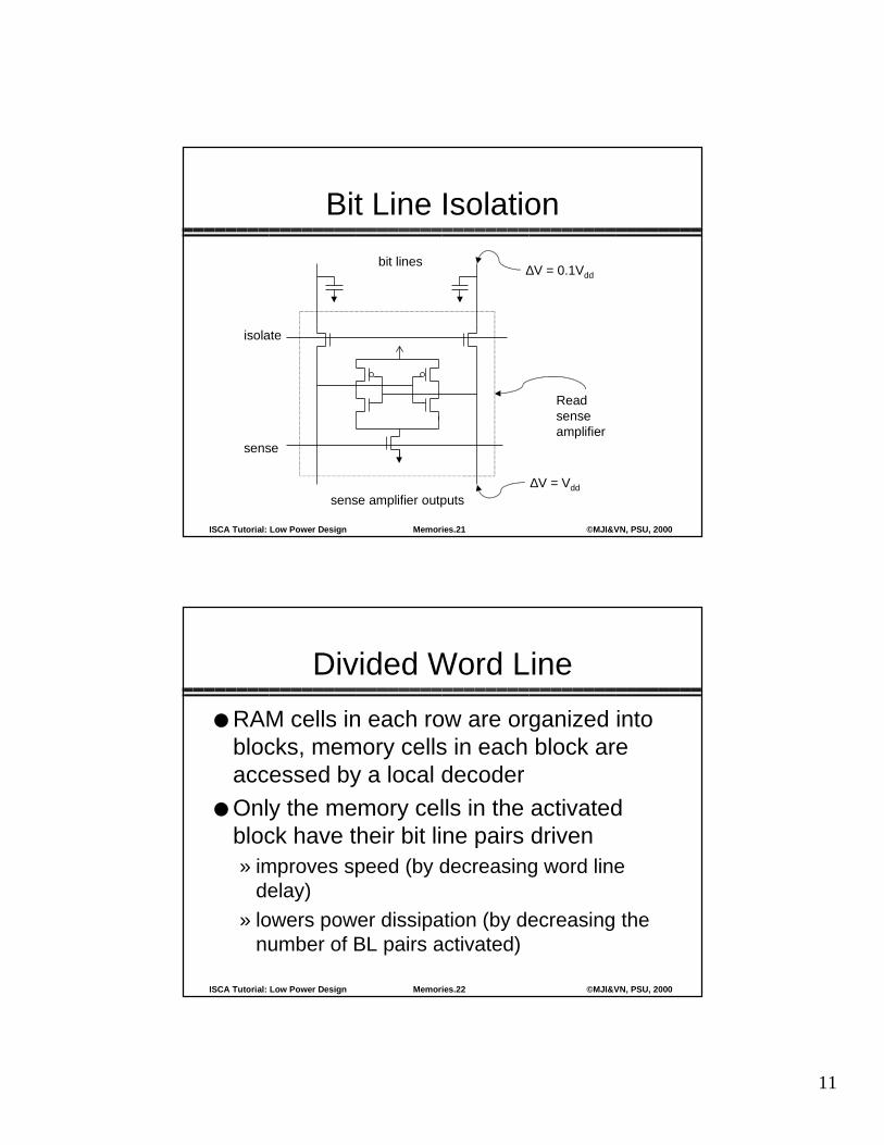
Bit Line Isolation
sense
Readsenseamplifier
bit lines
isolate
sense amplifier outputs
∆V = 0.1Vdd
∆V = Vdd
Memories.22ISCA Tutorial: Low Power Design ©MJI&VN, PSU, 2000
Divided Word Line
● RAM cells in each row are organized intoblocks, memory cells in each block areaccessed by a local decoder
● Only the memory cells in the activatedblock have their bit line pairs driven» improves speed (by decreasing word line
delay)» lowers power dissipation (by decreasing the
number of BL pairs activated)
12
Memories.23ISCA Tutorial: Low Power Design ©MJI&VN, PSU, 2000
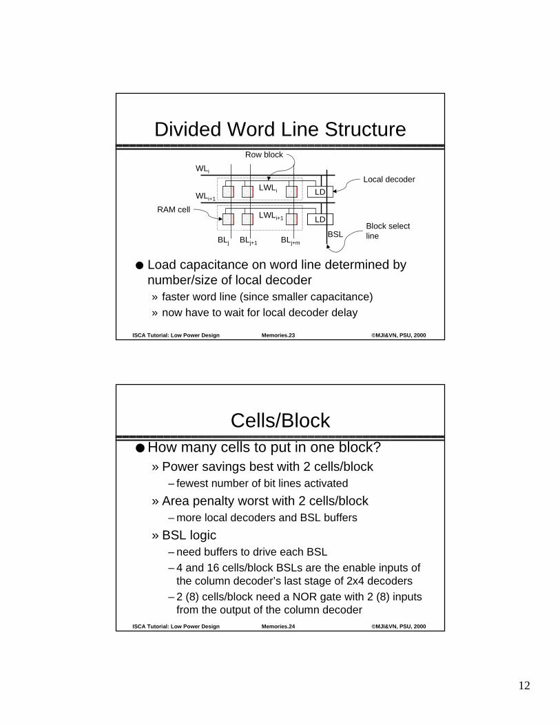
Divided Word Line Structure
● Load capacitance on word line determined bynumber/size of local decoder» faster word line (since smaller capacitance)» now have to wait for local decoder delay
BSL
LD
LD
WLi
WLi+1
LWLi
LWLi+1
Local decoder
Block selectline
RAM cell
BLj BLj+1 BLj+m
Row block
Memories.24ISCA Tutorial: Low Power Design ©MJI&VN, PSU, 2000
Cells/Block● How many cells to put in one block?
» Power savings best with 2 cells/block– fewest number of bit lines activated
» Area penalty worst with 2 cells/block– more local decoders and BSL buffers
» BSL logic– need buffers to drive each BSL– 4 and 16 cells/block BSLs are the enable inputs of
the column decoder’s last stage of 2x4 decoders– 2 (8) cells/block need a NOR gate with 2 (8) inputs
from the output of the column decoder
13
Memories.25ISCA Tutorial: Low Power Design ©MJI&VN, PSU, 2000
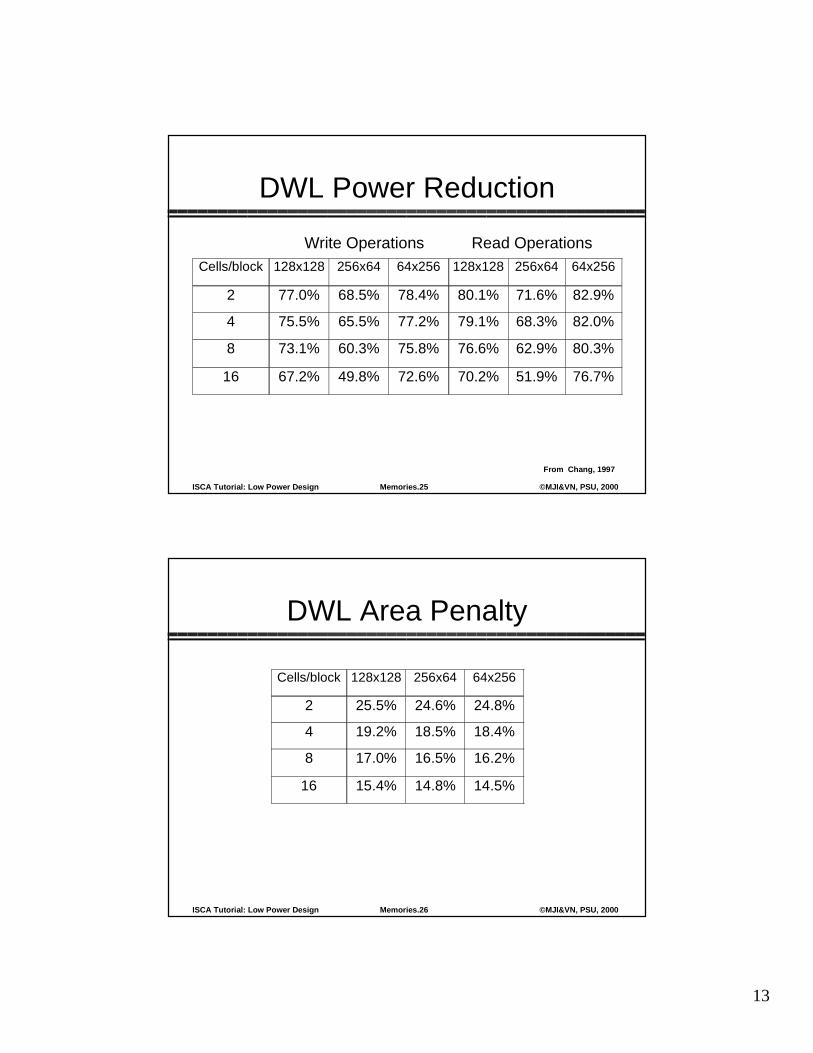
DWL Power Reduction
Cells/block 128x128 256x64 64x256 128x128 256x64 64x256
2 77.0% 68.5% 78.4% 80.1% 71.6% 82.9%
4 75.5% 65.5% 77.2% 79.1% 68.3% 82.0%
8 73.1% 60.3% 75.8% 76.6% 62.9% 80.3%
16 67.2% 49.8% 72.6% 70.2% 51.9% 76.7%
Write Operations Read Operations
From Chang, 1997
Memories.26ISCA Tutorial: Low Power Design ©MJI&VN, PSU, 2000
DWL Area Penalty
Cells/block 128x128 256x64 64x256
2 25.5% 24.6% 24.8%
4 19.2% 18.5% 18.4%
8 17.0% 16.5% 16.2%
16 15.4% 14.8% 14.5%

14
Memories.27ISCA Tutorial: Low Power Design ©MJI&VN, PSU, 2000
Bit Line Segmentation
● RAM cells in each column are organizedinto blocks selected by word lines
● Only the memory cells in the activatedblock present a load on the bit line» lowers power dissipation (by decreasing bit
line capacitance)» can use smaller sense amps
Memories.28ISCA Tutorial: Low Power Design ©MJI&VN, PSU, 2000
Bit Line Segmented Structure
● Address decoderidentifies the segmenttargeted by the rowaddress and isolates allbut the targeted segmentfrom the common bit line
● Has minimal effect onperformance
Switch toisolatesegment
LBLi+n,j
LBLi,j
BLj
WLi
SWLi+n,j
SWLi,j

15
Memories.29ISCA Tutorial: Low Power Design ©MJI&VN, PSU, 2000
Cache Power
● On-chip I$ and D$ (high speed SRAM)» DEC 21164a (2.0Vdd, 0.35µ, 400MHz, 30W max)
– I/D/L2 of 8/8/96KB and 1/1/3 associativity– caches dissipate 25% of the total chip power
» DEC SA-110 (2.0Vdd, 0.35µ, 233MHz, 1W typ)– I/D of 16/16KB and 32/32 associativity (no L2 on-chip)– I$ (D$) dissipate 27% (16%) of the total chip power
● Improving the power efficiency of caches iscritical to the overall system power
Memories.30ISCA Tutorial: Low Power Design ©MJI&VN, PSU, 2000
Cache Energy Consumption
● Energy Dissipated by Bitlines: precharge,read and write cycles
● Energy Dissipated by Wordlines: when aparticular row is being read or written
● Energy Dissipated by Address Decoders● Energy Dissipated by Peripheral Circuit -
comparators, cache control logic etc.● Off-Chip Main Memory Energy is based on
per-access cost

16
Memories.31ISCA Tutorial: Low Power Design ©MJI&VN, PSU, 2000
Analytical Energy ModelExample
● On-chip cacheEnergy = Ebus + Ecell + Epad + Emain…
Ecell = β*(wl_length)*(bl_length+4.8)*(Nhit + 2*Nmiss)wl_length = m*(T + 8L + St)bl_length = C/(m*L)
Nhit = number of hits; Nmiss = number of misses;C = cache size; L = cache line size in bytes; m = setassociativity; T = tag size in bits; St = # of status bitsper line; β = 1.44e-14 (technology parameter)
Memories.32ISCA Tutorial: Low Power Design ©MJI&VN, PSU, 2000
Cache Power Distribution
0
200
400
600
800
1000
1200
1400
1600
1800
ijp eg p erl fp p p avg
L 1 I$L 1 D $L 2
Pow
er in
mill
iwat
ts
Base Configuration: 4-way superscalar 32KB DM L1 I$ 32KB, 4-way SA L1 D$ 32B blocks, write back 128KB, 4-way SA L2 64B blocks, write back 1MB, 8-way SA off-chip L3 128B blocks, write thru
Interconnect widths 16B between L1 and L2 32B between L2 and L3 64B between L3 and MM
From Ghose, 1999
17
Memories.33ISCA Tutorial: Low Power Design ©MJI&VN, PSU, 2000
Low Power Cache Techniques
● SRAM power reduction● Cache block buffering● Cache subbanking● Divided word line● Multidivided module (MDM)● Modifications to CAM cell (for FA cache
and FA TLB)
Memories.34ISCA Tutorial: Low Power Design ©MJI&VN, PSU, 2000
Cache Block Buffering
● Check to see if data desired is in the dataoutput latch from the last cache access(i.e., in the same cache block)
● Saves energy since not accessing tag anddata arrays» minimal overhead hardware
● Can maintain performance of normal setassociative cache

18
Memories.35ISCA Tutorial: Low Power Design ©MJI&VN, PSU, 2000
Block Buffer Cache Structure
Tag Data
=
Tag Data
=
Address issued by CPU
last_set_#
=
disable sensing
Hit Desired word
Memories.36ISCA Tutorial: Low Power Design ©MJI&VN, PSU, 2000
Block Buffering Performance
0
300
600
900
1200
1500
1800
2100
2400
2700
3000
L 1 I$ L 1 D $ L 2 T ota l
0 b u ffers1 b u ffer2 b u ffers
Same base configuration 4-way superscalar 32KB DM L1 I$ ...
Pow
er in
mill
iwat
ts
From Ghose, 1999
19
Memories.37ISCA Tutorial: Low Power Design ©MJI&VN, PSU, 2000
TagTag
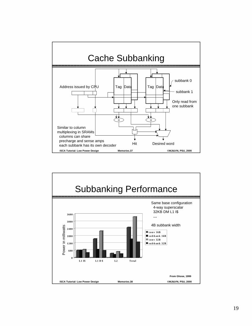
Cache Subbanking
Tag Data
=
Tag Data
=
Address issued by CPU
Hit Desired word
subbank 0
subbank 1
Similar to columnmultiplexing in SRAMs columns can share precharge and sense amps each subbank has its own decoder
Only read fromone subbank
Memories.38ISCA Tutorial: Low Power Design ©MJI&VN, PSU, 2000
Subbanking Performance
0
600
1200
1800
2400
3000
3600
L 1 I$ L 1 D $ L 2 T ota l
con v 16Bsu b b an k 16Bcon v 32Bsu b b an k 32B
Same base configuration 4-way superscalar 32KB DM L1 I$ …
4B subbank width
Pow
er in
mill
iwat
ts
From Ghose, 1999
20
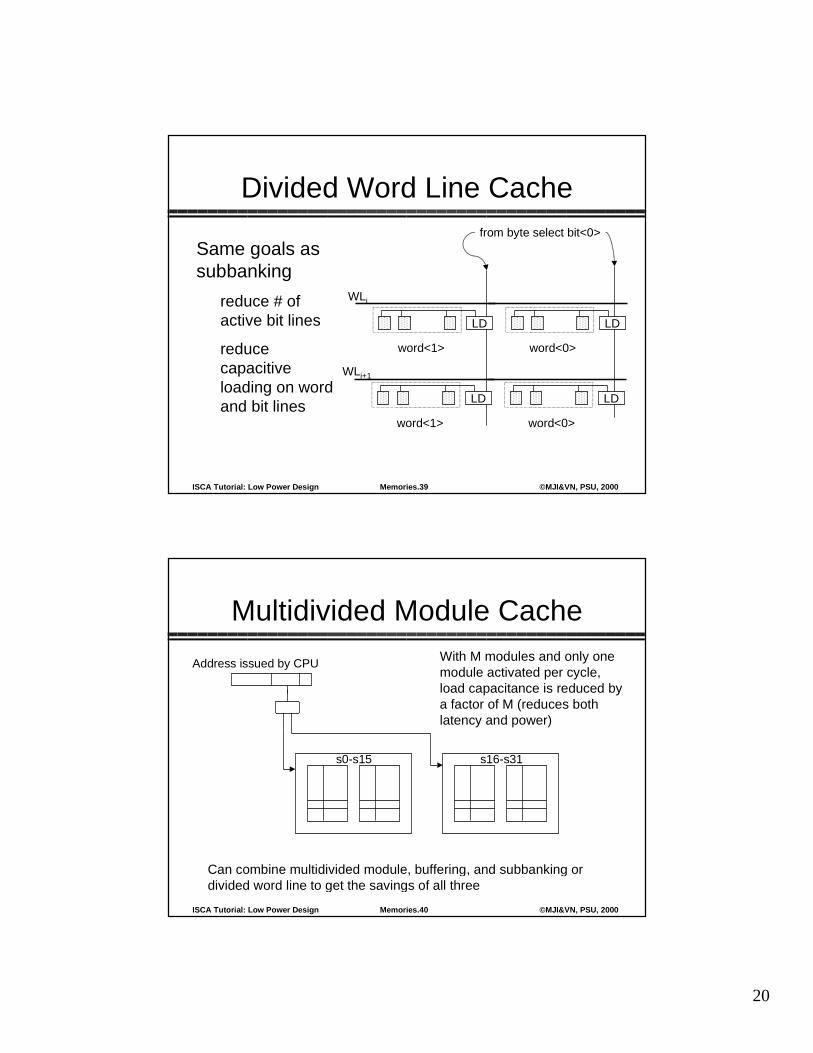
Memories.39ISCA Tutorial: Low Power Design ©MJI&VN, PSU, 2000
Divided Word Line Cache
LD
WLi+1
LD
word<1> word<0>
from byte select bit<0>
LD
WLi
LD
word<1> word<0>
Same goals assubbanking
reduce # ofactive bit lines
reducecapacitiveloading on wordand bit lines
Memories.40ISCA Tutorial: Low Power Design ©MJI&VN, PSU, 2000
Multidivided Module Cache
Address issued by CPU
s0-s15 s16-s31
With M modules and only onemodule activated per cycle,load capacitance is reduced bya factor of M (reduces bothlatency and power)
Can combine multidivided module, buffering, and subbanking ordivided word line to get the savings of all three

21
Memories.41ISCA Tutorial: Low Power Design ©MJI&VN, PSU, 2000
Translation Lookaside Buffers
● Small caches to speed up addresstranslation in processors with virtualmemory
● All addresses have to be translated beforecache access
» DEC SA-110 (2.0Vdd, 0.35µ, 233MHz, 1W typ)– I$ (D$) dissipate 27% (16%) of the total chip power– TLB 17% of total chip power
● I$ can be virtually indexed/virtually tagged
Memories.42ISCA Tutorial: Low Power Design ©MJI&VN, PSU, 2000
TLB StructureAddress issued by CPU (page size = index bits + byte select bits)
Tag Data
=
Tag Data
=
Hit Desired word
VA Tag PA
Most TLBs are small(<= 256 entries)and thus fully associative
Hit

22
Memories.43ISCA Tutorial: Low Power Design ©MJI&VN, PSU, 2000
TLB Power
0
10
20
30
40
50
60
70
80
32 64 12 8 25 6
D M2 S A4 S A8 S AFA
Pow
er in
mill
iwat
ts
From Juan, 1997
Memories.44ISCA Tutorial: Low Power Design ©MJI&VN, PSU, 2000
CAM Design
Read/Write Circuitry
Hit
match<0>
match<1>
match<2>
match<3>
match/write data
WL<0>
WL<1>
WL<2>
WL<3>
precharge/match
match
WLbit bit
word line<0>of data array

23
Memories.45ISCA Tutorial: Low Power Design ©MJI&VN, PSU, 2000
Low Power CAM Cell
match
WLbit bit
control
match
WLbit bit
Memories.46ISCA Tutorial: Low Power Design ©MJI&VN, PSU, 2000
Typical Memory Hierarchy
Control
Datapath
SecondaryStorage(Disk)
On-Chip Components
RegF
ile
MainMemory(DRAM)
SecondLevelCache
(SRAM)
Data
Cache
InstrC
ache
ITLB
DT
LB
DEC 21164a (2.0Vdd, 0.35µ, 400MHz, 30W max)
–caches dissipate 25% of the total chip power
DEC SA-110 (2.0Vdd, 0.35µ, 233MHz, 1W typ) – no L2 on-chip
–I$ (D$) dissipate 27% (16%) of the total chip power
eDRAM

24
Memories.47ISCA Tutorial: Low Power Design ©MJI&VN, PSU, 2000
Low Power DRAMs
● Conventional DRAMs refresh all rows witha fixed single time interval» read/write stalled while refreshing» refresh period -> tref
» DRAM power = k * (#read/writes + #ref)
● So have to worry about optimizing refreshoperation as well
Memories.48ISCA Tutorial: Low Power Design ©MJI&VN, PSU, 2000
Optimizing Refresh● Selective refresh architecture (SRA)
» add a valid bit to each memory row and onlyrefresh rows with valid bit set
» reduces refresh 5% to 80%
● Variable refresh architecture (VRA)» data retention time of each cell is different» add a refresh period table and refresh counter
to each row and refresh with the appropriateperiod to each row
» reduces refresh about 75%From Ohsawa, 1995

25
Memories.49ISCA Tutorial: Low Power Design ©MJI&VN, PSU, 2000
Application-Specific Memories
● Data and Code Compression» Custom instruction sets: ARM thumb code:
interleaving of 32-bit and 16-bit thumb codes» Reduces memory size» Reduces width of off-chip buses» location of compression unit is important» Compress only selective blocks
Memories.50ISCA Tutorial: Low Power Design ©MJI&VN, PSU, 2000
Hardware Code Compression
● Assuming only a subset of instr’s used,replace them with a shorter encoding toreduce memory bandwidth
memory
addresses
instructions
Core
IDTlogN bitsk bits
instructiondecompression table
(restores original format)

26
Memories.51ISCA Tutorial: Low Power Design ©MJI&VN, PSU, 2000
Other Techniques
● Customizing Memory Hierarchy» Close vs. far memory accesses» Close - faster, less energy consuming, smaller
caches» Energy per access increases monotonically
with memory size» Automatic memory partitioning
Memories.52ISCA Tutorial: Low Power Design ©MJI&VN, PSU, 2000
Memory Partitioning
● A memory partition is a set of memorybanks that can be independently selected
● Any address is stored into one and onlyone bank
● The total energy consumed by apartitioned is the sum of the energyconsumed by all its banks
● Partitions increasing selection logic costMacii, 2000
27
Memories.53ISCA Tutorial: Low Power Design ©MJI&VN, PSU, 2000
Scratch Pad Memory● Use of Scratch Pad Memory instead of
Caches for locality» Memory accesses of embedded software are
usually very localized» Map most frequent accessed locations onto
small on-chip memory» Caches have tag overhead - eliminate by
application specific decode logic» Map small set of most frequently accessed
addresses to consequetive locations in smallmemory Benini 2000
Memories.54ISCA Tutorial: Low Power Design ©MJI&VN, PSU, 2000
Key References, MemoriesAmrutur, Techniques to Reduce Power in Fast Wide Memories, Proc. of
SLPE, pp. 92-93, 1994.Angel, Survey of Low Power Techniques for ROMs, Proc. of SLPED, pp.
7-11, Aug. 1997.Chang, Power-Area Trade-Offs in Divided Word Line Memory Arrays,
Journal of Circuits, Systems, Computers, 7(1):49-57, 1997.Evans, Energy Consumption Modeling and Optimization for SRAMs, IEEE
Journal of SSC, 30(5):571-579, May 1995.Itoh, Low Power Memory Design, in Low Power Design Methodologies,
pp. 201-251, KAP, 1996.Ohsawa, Optimizing the DRAM Refresh Count, Proc. Of SLPED, pp. 82-
87, Aug 1998.Shimazaki, An Automatic Power-Save Cache Memory, Proc. Of SLPE, pp.
58-56, 1995.Yoshimoto, A Divided Word Line Structure in SRAMs, IEEE Journal of
SSC, 18:479-485, 1983.

28
Memories.55ISCA Tutorial: Low Power Design ©MJI&VN, PSU, 2000
Key References, CachesGhose, Reducing Power in SuperScalar Processor Caches Using
Subbanking, Multiple Line Buffers and Bit-Line Segmentation, Proc. ofISLPED, pp. 70-75, 1999.
Juan, Reducing TLB Power Requirements, Proc. of ISLPED, pp. 196-201, Aug 1997.
Kin, The Filter Cache: An Energy-Efficient Memory Structure, Proc. ofMICRO, pp. 184-193, Dec. 1997.
Ko, Energy Optimization of Multilevel Cache Architectures, IEEE Trans.On VLSI Systems, 6(2):299-308, June 1998.
Panwar, Reducing the Frequency of Tag Compares for Low Power I$Designs, Proc. of ISLPD, pp. 57-62, 1995.
Shimazaki, An Automatic Power-Save Cache Memory, Proc. of SLPE,pp. 58-59, 1995.
Su, Cache Design Tradeoffs for Power and Performance Optimization,Proc. of ISLPD, pp. 63-68, 1995.