Tuning the graphene work function by electric field effect
12
1 Tuning the graphene work function by electric field effect Young-Jun Yu 1, 2 , Yue Zhao 1 , Sunmin Ryu 3 , Louis E. Brus 3 , Kwang S. Kim 2 and Philip Kim 1* 1 Department of Physics, Columbia University, New York, New York 10027, USA 2 Center for Superfunctional Materials, Department of Chemistry, Pohang University of Science and Technology, Hyojadong, Namgu, Pohang 790-784, Korea 3 Department of Chemistry, Columbia University, New York, New York 10027, USA *E-mail: pk2015@ columbia.edu Abstract We report variation of the work function for single and bi-layer graphene devices measured by scanning Kelvin probe microscopy (SKPM). Using the electric field effect, the work function of graphene can be adjusted as the gate voltage tunes the Fermi level across the charge neutrality point. Upon biasing the device, the surface potential map obtained by SKPM provides a reliable way to measure the contact resistance of individual electrodes contacting graphene. High conductivity 1,2 and low optical absorption 3,4 make graphene an attractive material for use as a flexible transparent conductive electrode 5-8 . This atomically thin carbon layer provides the additional benefit that its work function can be adjusted by the electric field effect (EFE). Since the band alignment of two different materials is determined by their respective work functions, control over the graphene work function is the key to reducing the contact barriers of graphene top electrode devices 9, 10 . Previous scanning probe based studies 11-13 reveal that the work function of graphene is in a similar range to that of graphite, ~4.6 eV 14 , and depends sensitively on the number of layers 15, 16 . However, the active controlling of the graphene work function has yet to be demonstrated. In this study, we apply Scanning Kelvin probe microscope (SKPM) techniques to back-gated graphene devices and demonstrate that the work function can be controlled over a wide range by EFE induced modulation of carrier concentration. SKPM is an atomic force microscope (AFM) based experimental technique that can map the surface potential variation of a sample surface relative to that of metallic tip 17 . The change of work function is ascribed by the Fermi level shift due to the EFE induced carrier doping and is well quantified by the electronic band structure of graphene. On biased graphene devices, SKPM also allows us to accurately measure graphene/metal contact resistances by mapping the surface potential of a device. The wide range of control over the work function demonstrated here suggests graphene as an ideal material for applications where work function optimization is important. Graphene samples were prepared by mechanical exfoliation 18 on Si wafers covered with 300 nm thick SiO 2 and then Cr/Au electrodes (5 nm/30 nm thickness) were fabricated by
Transcript of Tuning the graphene work function by electric field effect

1
Tuning the graphene work function by electric field effect
Young-Jun Yu1, 2, Yue Zhao1, Sunmin Ryu3, Louis E. Brus3, Kwang S. Kim2 and Philip Kim1*
1Department of Physics, Columbia University, New York, New York 10027, USA
2 Center for Superfunctional Materials, Department of Chemistry, Pohang University of Science and Technology, Hyojadong, Namgu, Pohang 790-784, Korea
3Department of Chemistry, Columbia University, New York, New York 10027, USA *E-mail: pk2015@ columbia.edu
Abstract We report variation of the work function for single and bi-layer graphene devices measured by scanning Kelvin probe microscopy (SKPM). Using the electric field effect, the work function of graphene can be adjusted as the gate voltage tunes the Fermi level across the charge neutrality point. Upon biasing the device, the surface potential map obtained by SKPM provides a reliable way to measure the contact resistance of individual electrodes contacting graphene.
High conductivity1,2 and low optical absorption3,4 make graphene an attractive material for use as a flexible transparent conductive electrode5-8. This atomically thin carbon layer provides the additional benefit that its work function can be adjusted by the electric field effect (EFE). Since the band alignment of two different materials is determined by their respective work functions, control over the graphene work function is the key to reducing the contact barriers of graphene top electrode devices9, 10. Previous scanning probe based studies11-13 reveal that the work function of graphene is in a similar range to that of graphite, ~4.6 eV14, and depends sensitively on the number of layers15, 16. However, the active controlling of the graphene work function has yet to be demonstrated.
In this study, we apply Scanning Kelvin probe microscope (SKPM) techniques to back-gated graphene devices and demonstrate that the work function can be controlled over a wide range by EFE induced modulation of carrier concentration. SKPM is an atomic force microscope (AFM) based experimental technique that can map the surface potential variation of a sample surface relative to that of metallic tip17. The change of work function is ascribed by the Fermi level shift due to the EFE induced carrier doping and is well quantified by the electronic band structure of graphene. On biased graphene devices, SKPM also allows us to accurately measure graphene/metal contact resistances by mapping the surface potential of a device. The wide range of control over the work function demonstrated here suggests graphene as an ideal material for applications where work function optimization is important.
Graphene samples were prepared by mechanical exfoliation18 on Si wafers covered with 300 nm thick SiO2 and then Cr/Au electrodes (5 nm/30 nm thickness) were fabricated by

2
standard electron beam lithography. The thickness of each graphene samples was characterized by Raman spectroscopy (see Supporting information, Fig. S1). In this work, we have studied with three single layer graphene (SLG) and two bilayer graphene (BLG) transistors. Fig. 1(a) shows a schematic diagram of the simultaneous SKPM experiments with the EFE induced carrier modulation. The SKPM measurements were performed by commercial atomic force microscope (XE-100, Park Systems Corp.) in air and dry nitrogen environment at room temperature. During observing SKPM data, we applied AC voltage amplitude of ~0.3-0.5 V and a frequency of 17 kHz to a Cr/Au coated probe. The SKPM images were obtained with two-way scan method to avoid topographic artifacts. The first scan was for topography by non-contact mode with dithering resonant frequency ~ 120-170 kHz and the second scan was for SKPM image with 10~30 nm constant height mode.
The carrier density, and hence the Fermi energy, EF, of the graphene, is controlled by the gate voltage Vg applied to the degenerately doped Si substrate. Fig. 1(b)-(e) shows the optical, atomic force microscopy (AFM) topographic, and surface potential images of one of the SLG devices used in this experiment. In general, the local surface potential, VCPD, obtained from the contact potential difference between the SKPM probe and local surface17, is sensitively influenced by Vg. By comparing VCPD maps taken at Vg =0 (Fig. 1(d)) and 10 V (Fig. 1(e)), we notice a much larger signal contrast at higher Vg. In particular, VCPD tends to increase to values comparable to Vg on the insulating SiO2 substrate. This indicates that the unscreened electric field from the back gate is the dominant source for the contrast in VCPD image in the bare SiO2 regions. In order to minimize a direct exposure of the SKPM probe to this long range electrostatic influence, we limit our surface potential analysis to areas within the conducting part of the device, where the subtle local surface potential variation can be readily probed.
Figure 1 (a) Schematic diagram for measuring the EFE modulation of the surface potential of graphene devices using the SKPM. Gate voltage Vg is applied to the degenerately doped Si substrate and the electrodes of graphene device are grounded. (b)-(e) From top to down, optical image (b), AFM topography (c), and SKPM images of graphene device Vg = 0 V (d) and 10 V (e), respectively.

3
Utilizing multi-terminal device geometry, we carry out a comparison study of the surface potential (Fig. 2(a)) and transport measurement (Fig. 2(b)) on the same device as a function of Vg. In the particular device shown in this figure, we determine the charge neutral gate voltage VD = 48 V, from the gate voltage corresponding to a sharp resistance peak. In the surface potential map where Vg is fixed, we observe a stepwise increase of VCPD at the junctions between graphene and electrodes regions, but no significant spatial variation within each region. Similar features are observed at different values of Vg (Fig. 2(c)), where the overall line profiles of VCPD in the two regions shift upward with a common background
Figure 2 (a) Top panel shows an AFM topography of the device. The surface potential map of a selected area far from the graphene edges (marked by a dotted line box) is analyzed in detail in order to minimze the effect from unscreened long ranged electrostatic force from the gate. Small spatial variations in the topographic and SKPM signals are found to be correlated on the top of the graphene surface. Vg = 55 V in this image. A schematic energy alignment diagram for the graphene sample and the metallic elecrode is displayed where Evac, EF, and ED are representing the vacuum energy level, Fermi energy and the charge neutrality point of graphene, respectively. (b) Transport measurement using the two outer terminals as shown in the inset. From the peak position we have VD = 48 V. (c) The surface potential profile along the x-axis (averaged over the y-axis) at different gate voltages Vg (at every 1 V from 39 to 60 V). (d) The CPD of graphene Vg
CPD and electrode VeCPD at different gate
voltages obtained from the average surface potential in the selected gray and red shaded area in (c). The inset shows VCPD =Vg
CPD -VeCPD as a function of Vg. The vertical dashed line indicates Vg = VD where
the corresponding VCPD is highlighted by the horizontal arrow.

4
as Vg increases. This background signal is due to the unscreened long-range electrostatic interaction between the conducting cantilever probe and the back gate, and thus is insensitive to a small spatial position change of the SKPM tip. Since Vg should not influence the local surface potential in metallic electrode, the back ground signal on the metal electrode surface can serve to separate the spatially constant background from the relative change in the local surface potential. In particular, the EFE induced local surface potential change in graphene, VCPD, can be obtained by e
CPDg
CPDCPD VVV , where VeCPD and Vg
CPD are the average
VCPD in the electrode and the graphene, respectively (Fig. 2(d) inset). Interestingly, a sudden change VCPD is observed at the charge neutrality point (Vg= VD), as indicated by the vertical dashed line.
Similar features are always present at the neutrality point in other SLG samples studied in this experiment. We also perform similar measurement of VCPD on BLG samples. Similar to the SLG, VCPD of BLG can be modulated by applied gate voltage (see Supplementary information, Fig. S2). Unlike the SLG samples, however, there is no such sudden change of VCPD at the BLG charge neutrality point, implying the difference of the electronic structures of the samples as we will discuss later.
Figure 3 (a) Measured work function of SLG samples (filled symbols) and BLG samples (open symbols) as a function of Vg - VD. SLG samples show larger work function changes (shaded in red) while the BLG samples exhibit less changes (shaded in blue), where shaded areas indicate the uncertainty for the work function offset due to the adsorbate induced surface dipole layers (see supplementary materials). The filled green, red and purple symbols are SLG data taken in air. Other data were taken in dry nitrogen environment. (b) Schematic diagram for the energy level alignment in the SKPM tip and graphene samples. The left panel shows the work function of tip relative to the vacuum level. The right panel shows the relation between Wsample, W
0gr, EF, and Wa, defined in the text
relative to the vacuum level. (c) The Fermi energy variation of SLG and BLG as a function of Vg-VD. Symbols are same as in (a). EF is deduced from Wsample, by subtracting off W0
gr +Wa, whose values obtained at the charge neutrality point Vg = VD. The dashed curve and line are the EF
SLG and EFBLG from
the band structure calculations.
5
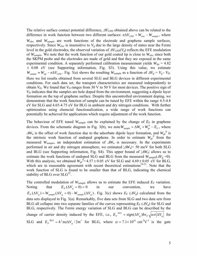
The relative surface contact potential difference, VCPD obtained above can be related to the difference in work function between two different surfaces: sampleelecCPD WWVe , where
Welec and Wsample are work functions of the electrode and graphene sample surfaces, respectively. Since Welec is insensitive to Vg due to the large density of states near the Fermi level in the gold electrodes, the observed variation of VCPD(Vg) reflects the EFE modulation of Wsample. We note that the work function of our gold coated tip is close to Welec since both the SKPM probe and the electrodes are made of gold and that they are exposed in the same experimental condition. A separately performed calibration measurement yields Wtip = 4.82 0.08 eV (see Supporting information, Fig. S3). Using this value, we estimate
CPDtipsample VeWW . Fig. 3(a) shows the resulting Wsample as a function of Vg = Vg - VD.
Here we list results obtained from several SLG and BLG devices in different experimental conditions. For each data set, the transport characteristics are measured independently to obtain VD. We found that VD ranges from 30 V to 50 V for most devices. The positive sign of VD indicates that the samples are hole doped from the environment, suggesting a dipole layer formation on the top of graphene surface. Despite this uncontrolled environment doping, we demonstrate that the work function of sample can be tuned by EFE within the range 4.5-4.8 eV for SLG and 4.65-4.75 eV for BLG in ambient and dry nitrogen conditions. With further optimization using chemcial functionalization, a wide range of work functions can potentially be achieved for applications which require adjustment of the work function.
The behaviour of EFE tuned Wsample can be explained by the change of EF in graphene devices. From the schematic diagram in Fig. 3(b), we note Fgrasample EWWW 0 , where
Wa is the offset of work function due to the adsorbate dipole layer formation, and Wgr0 is
the intrinsic work function of undoped graphene. In order to estimate Wgr0 from the
measured Wsample, an independent estimation of Wa is necessary. In the experiments performed in air and dry nitrogen atmosphere, we estimated |Wa|< 50 meV for both SLG and BLG (see Supporting information, Fig. S4). This upper bound of |Wa| allows us to estimate the work functions of undoped SLG and BLG from the measured Wsample(Vg =0). With this analysis, we obtained Wgr
0= 05.057.4 eV for SLG and 05.069.4 eV for BLG, which are in reasonable agreement with recent theoretical estimations19-21. Note that the work function of SLG is found to be smaller than that of BLG, indicating the chemical stability of BLG over SLG22.
The controlled modulation of Wsample allows us to estimate the EFE induced EF variation. Noting that 0)0( gF VE in our convention, we have
)()0()( gsamplegsamplegF VWVWVE . Fig. 3(c) shows EF (Vg) calculated from the
data sets displayed in Fig. 3(a). Remarkably, five data sets from SLG and two data sets from BLG all collapse into two separate families of the curves representing EF (Vg) for SLG and BLG, respectively. The Fermi energy variation of SLG and BLG can be described by the
change of carrier density induced by the EFE, i.e., gFgSLG
F VvVsignE )( for
SLG and *2 2/ mVE gBLG
F for BLG, where 10101.7 cm-2V-1 is the gate
6
capacitance in electron charge, vF = 6101 m/sec is the Fermi velocity of SLG, and m* = 0.033 me is the effective mass of carrier in BLG relative to the bare electron mass me obtained from the literature23-25. Employing these values, we plot EF
SLG (dashed curve) and EF
BLG (dashed line) in Fig. 3(c), where excellent agreements are found without any fitting parameters, indicating the observed work function variation is ascribed solely to the EFE modulation of EF.
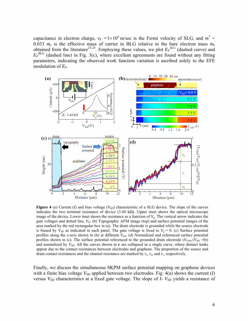
Finally, we discuss the simultaneous SKPM surface potential mapping on graphene devices with a finite bias voltage VSD applied between two electrodes. Fig. 4(a) shows the current (I) versus VSD characteristics at a fixed gate voltage. The slope of I- VSD yields a resistance of
Figure 4 (a) Current (I) and bias voltage (VSD) characteristic of a SLG device. The slope of the curves indicates the two terminal resistance of device (3.44 kΩ). Upper inset shows the optical microscope image of the device. Lower inset shows the resistance as a function of Vg. The vertical arrow indicates the gate voltages and dotted line, VD. (b) Topographic AFM image (top) and surface potential images of the area marked by the red rectangular box in (a). The drain electrode is grounded while the source electrode is biased by VSD as indicated in each panel. The gate voltage is fixed to Vg = 0. (c) Surface potential profiles along the x-axis shown in (b) at different VSD. (d) Normalized and referenced surface potential profiles shown in (c). The surface potential referenced to the grounded drain electrode (VCPD (VSD =0)) and normalized by VSD. All the curves shown in c are collapsed in a single curve, where distinct kinks appear due to the contact resistances between electrodes and graphene. The proportion of the source and drain contact resistances and the channel resistance are marked by rs, rd, and rc, respectively.
7
3.44 kΩ which includes the contributions of contact resistances between each electrode and the graphene channel. The simultaneous SKPM surface potential mapping provides a way to estimate these contributions independently. Fig. 4(b) displays topographic and surface potential mapping of the same device with increasing VSD from 0 to 2 V. The surface potential of the grounded source electrode remains close to 0 V, while the surface potential of the biased drain electrode shifts upward as VSD increases. From the horizontal profile of these images (Fig. 4(c)), we clearly observe linearly increasing VCPD in the channel and kinks in VCPD at the junctions. We attribute these sudden potential drops to the contact resistance between the electrodes and graphene. By taking the grounded drain electrode as the reference point (VCPD (VSD=0)) and normalizing the VCPD by VSD, all the surface potential profiles at different VSD collapse into one universal curve [VCPD (VSD) - VCPD (VSD =0)] / VSD
(Fig. 4(d)). The vertical ratios between the kinks and the slope correspond to the source and drain contact resistances (rs & rd) and graphene channel resistance (rc). Considering that the total two terminal resistance of this device is 3.44 kΩ, we obtain rd:rc:rs=0.5: 1.7: 1.24 kΩ for this particular device.
In conclusion, by employing a gate modulated SKPM measurement, we have demonstrated that the work function of graphene can be substantially adjusted by EFE. This widely tunable work function makes graphene an attractive material for low contact barrier electrodes. The simultaneous SKPM surface potential imaging allows us to evaluate the contacts of graphene devices.
Acknowledgements. We thank Mark S. Hybertsen for helpful discussion. This work was supported by DOE (No. DEFG02-05ER46215, DE-FG02-98ER-14861), ONR (N000140610138), NSF NSEC (No. CHE-0117752), NYSTAR, FENA MARCO center, DARPA (FA8650-08-C-7838) through CERA program, KICOS(GRL), KOSEF (EPB Center: R11-2008-052-01000), and BK21(KRF).
Supporting Information Available: Optical images and Raman spectroscopy of single-layer graphene (SLG) and bi-layer graphene (BLG) for confirming thickness, the surface potential modulation of a BLG device by the change of gate voltage, the calibration of Work function of SKPM probes, Work function offset of SLG and BLG.
Reference
(1) Bolotin, K.; Sikes, K. J.; Jiang, Z.; Klima, M.; Fudenberg, G.; Hone, J.; Kim, P.; Stomer, H. L. Solid State Commun. 146, 351-355 (2008)
(2) Du, X.; Skachko, I.; Barker, A.; Andrei, E. Y. Nature Nanotechnol. 3, 491-495 (2008). (3) Nair, R. R.; Blake, P.; Grigorenko, A. N.; Novoselov, K. S.; Booth, T. J.; Stauber, T.;
Peres, N. M.; Geim, A. K. Science 320, 1308 (2008). (4) Mak, K. F.; Sfeir, M. Y.; Wu, Y.; Lui, C. H.; Misewich, J. A.; Heinz, T. F. Phys. Rev. Lett.
101, 196405 (2008). (5) Li, X.; Zhang, G.; Bai, X.; Sun, X.; Wang, X.; Wang, E.; Dai, H. Nature Nanotechnol. 3,
538-542 (2008) (6) Eda, G.; Fanchini, G.; Chhowalla, M. Nature Nanotechnol. 3, 270-274 (2008) (7) Reina, A.; Jia, X.; Ho, J.; Nezich, D.; Son, H.; Bulovic, V.; Dresselhaus, M. S.; Kong, J.

8
Nano lett. 9, 30-35 (2009) (8) Kim, K. S.; Zhao, Y.; Jang, H.; Lee, S. Y.; Kim, J. M.; Kim, K. S.; Ahn, J. –H.; Kim, P.;
Choi, J. –Y.; Hong, B. H. Nature 457, 706-710 (2009) (9) Ishii, H.; Sugiyama, K.; Ito, E.; Seki, K. Adv. Mater. 11, 605-625 (1999) (10) Jiang, J.; Krauss, T. D.; Brus, L. E. J. Phys. Chem. B. 104, 11936-11941 (2000) (11) Filleter, T.; Emtsev, K. V.; Seyller, Th.; Bennewitz, R. Appl. Phys. Lett. 93, 133117
(2008) (12) Datta, S. S.; Strachan, D. R.; Mele, E. J.; Johnson, A. T. C. Nano lett. 9, 7-11 (2009) (13) Shi, Y.; Dong, X.; Chen, P.; Wang, J.; Li, L. -J. Phys. Rev. B 79, 115402 (2009) (14) Takahashi, T.; Tokailin, H.; Sagawa, T.; Phys. Rev. B 32, 8317-8324 (1985) (15) Giovannetti, G.; Khomyakov, P. A.; Brocks, G.; Karpan, V. M.; Van den Brink, J.;
Kelly, P. J. Phys. Rev. Lett. 101, 026803 (2008) (16) Hibino, H.; Kageshima, H.; Kotsugi, M.; Maeda, F.; Guo, F. –Z.; Watanabe, Y. Phys.
Rev. B. 79, 125437 (2009) (17) Rosenwaks, Y.; Shiker, R.; Glatzel, Th.; Sadewasser, S. Phys. Rev. B 70, 085320
(2004) (18) Novoselov, K. S.; Jiang, D.; Schedin, F.; Booth, T. J.; Khotkevich, V. V.; Morozov, S.
V.; Geim, A. K. Proc. Natl. Acad. Sci. USA 102, 10451-10453 (2005) (19) Shan, B.; Cho, K. Phys. Rev. Lett. 94, 236602 (2005) (20) Ooi, N.; Rairkar, A.; Adams, J. B. Carbon 44, 231-242 (2006) (21) Sque, S. J.; Jones, R.; Briddon, P. R. Phys. Stat. Sol. 204, 3078-3084 (2007) (22) Liu, L.; Ryu, S.; Tomasik, M. R.; Stolyarova, E.; Jung, N.; Hybertsen, M. S.;
Steigerwald, M. L.; Brus, L. E.; Flynn, G. W. Nano lett. 8, 1965-1970 (2008) (23) Li, Z. Q.; Henriksen, E. A.; Jiang, Z.; Hao, Z.; Martin, M. C.; Kim, P.; Stomer, H. L.;
Basov, D. N. Nature Phys. 4, 532-535 (2008) (24) Henriksen, E. A.; Jiang, Z.; Tung, L. –C.; Schwartz, M. E.; Takita, M.; Wang, Y. –J.;
Kim, P.; Stormer, H. L. Phys. Rev. Lett. 100, 087403 (2008) (25) Yan, J.; Henriksen, E. A.; Kim, P.; Pinczuk, A. Phys. Rev. Lett. 101, 136804 (2008)

9
Supplementary information
1. Confirmation the thickness of graphene sheets with Raman characterization
In this experiment, we employ three SLG and two BLG devices. Raman spectroscopy (Fig. S1) is used to estimate the thickness of the graphene layers.
Figure S1. Insets show the optical images of three SLG and two BLG devices. The main panel shows D* resonance peaks which display the characteristic difference between SLG and BLG samples [S1]. 512 nm wave length laser is used for the excitation.
[S1] Ferrari, A. C., Meyer, J. C., Scardaci, V., Casiraghi, C., Lazzeri, M., Mauri, F., Piscanec, S., Jiang, D., Novoselov, K. S., Roth, S. & Geim, A. K. Raman spectrum of graphene and graphene layers. Phys. Rev. Lett. 97, 187401 (2006)

10
2. Field Effect modulation of surface potential in bilayer graphene
Figure S2. (a) Top panel shows an AFM topography of graphene channels with electrodes. The surface potential map of a selected area far from the graphene edges (marked by a dotted line box) is analyzed in detail in order to minimze the effect from unscreened long ranged electrostatic force from the gate. Vg = 51 V in this image. (b) From the transport measurements using the two outer terminals as shown in the schematic diagram in the optical image inset, we obtain VD = 37 V. (c) Surface potential profile along the x-axis (averaged over the y-axis) at different gate voltages Vg (at every 2 V from 17 to 53 V). (d) The CPD of graphene Vg
CPD and electrode VeCPD at different gate voltages obtained form the
aveage surface potential in the selected gray and red filled area shown in (c). The inset shows VCPD =Vg
CPD -VeCPD as a function of Vg. The vertical dashed line indicates Vg = VD
where the corresponding VCPD is highlighted by the horizontal arrow.

11
3. Calibration of SKPM probe with HOPG
In Fig.S3, the contact potential differences (VCPD) between gold coated SKPM probes and highly oriented pyrolytic graphite (HOPG) are VCPD = -0.453, -0.132, -0.179 and -0.133 V. Thus, the averaged VCPD between SKPM probes and HOPG is -0.22 0.08 V. The work function of the SKPM probes (Wtip) is estimated to be 4.82 0.08 eV by subtracting eVCPD
(=-0.22 0.08 eV) from the work function of HOPG, WH (=4.6 eV) [S2, S3].
Figure S3. Variation of electric force microscope (EFM) cantilever amplitude is plotted as the function of the tip bias voltage relative to the HOPG substrate. The left figure shows a schematic diagram of experiment and the relationship between the Fermi energy and the work function of SKPM probe and HOPG. The right inset show the detailed plot of the zero bias regime in the green dotted box of the left figure. The sample is homogeneous and there is no back gate voltage to create a long range unscreened electrostatic force. Therefore we do not need to subtract off any electrostatic background signal in this tip calibration process
[S2] Takahashi, T., Tokailin, H. & Sagawa, T. Angle-resolved ultraviolet photoelectron spectroscopy of the unoccupied band structure of graphite. Phys. Rev. B 32, 8317-8324 (1985)
[S3] Suzuki, S., Bower, C., Watanabe, Y. & Zhou, O. Work function and valence band states of pristine and Cs-intercalated single-walled carbon nanotube bundles Appl. Phys. Lett. 76, 4007-4009 (2000)

12
4. Variation of the work function offset due to the adsorbate dipole layer formation
The range of the work function offset due to the adsorption of molecules from the environment can be estimated from the measured work function at the charge neutrality point, W sample(Vg=VD) = W0
gr+Wa. Fig.S4 shows W0gr+Wa as a function of VD for several
SLG (filled symbols) and BLG (open symbols) samples. Despite different sample preparation and different environmental conditions of the experiment (i.e., air versus dry nitrogen), which results in a wide variation of VD, the difference in work function is smaller than 50 meV. Noting that Wa depends sensitively on VD, we thus estimate that |Wa |< 50 meV for the SLG samples. Since we do not see a specific trend of Wa as a function of VD, the work function of intrinsic graphene is obtained from the mean value of W
sample(Vg=VD), where we obtained 4.57 eV for SLG (black dotted line) and 4.69 eV for BLG (red dotted line).
Figure S4. The work function (W0gr+Wa) of SLG (filled symbols) and BLG (open
symbols) at the charge neutrality points (VD) from Fig. 3(a). The shade in red denotes the deviation ( 50 meV) of work function offset (Wa) of SLG devices studied in this work. The black and red dotted line is the averaged work function (W0
gr) of SLG (4.57 eV) and BLG (4.69 eV), respectively.


![Thermal conductivity reduction in graphene with …...rounding the thermal transport properties. As regards the heat transport of tuning graphene, investigations of isotope [18], nitrogen](https://static.fdocuments.us/doc/165x107/5fda9edff35a643bca2fc359/thermal-conductivity-reduction-in-graphene-with-rounding-the-thermal-transport.jpg)