
Tuning Size and Light Emission Characteristics of CDSES ...
73
University of Wisconsin Milwaukee UWM Digital Commons eses and Dissertations May 2019 Tuning Size and Light Emission Characteristics of CDSES/ZNS Alloyed Core-shell Quantum Dots By Alcohol John Casey Marnocha University of Wisconsin-Milwaukee Follow this and additional works at: hps://dc.uwm.edu/etd Part of the Electrical and Electronics Commons is esis is brought to you for free and open access by UWM Digital Commons. It has been accepted for inclusion in eses and Dissertations by an authorized administrator of UWM Digital Commons. For more information, please contact [email protected]. Recommended Citation Marnocha, John Casey, "Tuning Size and Light Emission Characteristics of CDSES/ZNS Alloyed Core-shell Quantum Dots By Alcohol" (2019). eses and Dissertations. 2098. hps://dc.uwm.edu/etd/2098
Transcript of Tuning Size and Light Emission Characteristics of CDSES ...

University of Wisconsin MilwaukeeUWM Digital Commons
Theses and Dissertations
May 2019
Tuning Size and Light Emission Characteristics ofCDSES/ZNS Alloyed Core-shell Quantum DotsBy AlcoholJohn Casey MarnochaUniversity of Wisconsin-Milwaukee
Follow this and additional works at: https://dc.uwm.edu/etdPart of the Electrical and Electronics Commons
This Thesis is brought to you for free and open access by UWM Digital Commons. It has been accepted for inclusion in Theses and Dissertations by anauthorized administrator of UWM Digital Commons. For more information, please contact [email protected].
Recommended CitationMarnocha, John Casey, "Tuning Size and Light Emission Characteristics of CDSES/ZNS Alloyed Core-shell Quantum Dots ByAlcohol" (2019). Theses and Dissertations. 2098.https://dc.uwm.edu/etd/2098

TUNING SIZE AND LIGHT EMISSION CHARACTERISTICS OF
CdSe1−xSx/ZnS ALLOYED CORE-SHELL QUANTUM DOTS BY ALCOHOL
by
J. Casey Marnocha
A Thesis Submitted in
Partial Fulfillment of the
Requirements for the Degree of
Master of Science
in Engineering
at
The University of Wisconsin-Milwaukee
May 2019

ABSTRACT
TUNING SIZE AND LIGHT EMISSION CHARACTERISTICS OF
CdSe1−xSx/ZnS ALLOYED CORE-SHELL QUANTUM DOTS BY ALCOHOL
by
J. Casey Marnocha
The University of Wisconsin-Milwaukee, 2019
Under the Supervision of Professor Nikolai Kouklin
In this thesis, a one-step isotropic down-tuning of the size of alloyed CdSe1−xSx/ZnS core-
shell quantum dots is developed by vapor and liquid-phase etching using a ∼ 10 : 1 isopropyl
alcohol to water solution. The results of spectroscopic studies confirm continuous variation
of the excitonic emission color from red to green for samples treated for up to 15 mins using
a vapor-based method. According to HRTEM characterizations, the shift is consistent with
a diameter reduction of quantum dots that proceeds at the average rate of ∼ 1.3 A/min.
The emission intensity while seen to undergo an initial drop due to the shell removal,
was to found to remain largely unchanged with increased treatment durations. The study
presents a technologically viable alternative to adjusting the size and, in turn, the optoelec-
tronic characteristics of core-shell quantum dots and nanocrystals in II-VI semiconductor
systems.
ii

c© Copyright by J. Casey Marnocha, 2019
All Rights Reserved
iii

For Sonja and Cadence...
iv

TABLE OF CONTENTS
1 Overview 1
1.1 Introduction . . . . . . . . . . . . . . . . . . . . . . . . . . . . . . . . . . . . 1
1.2 Synthesis Techniques . . . . . . . . . . . . . . . . . . . . . . . . . . . . . . . 2
1.2.1 Molecular Beam Epitaxy . . . . . . . . . . . . . . . . . . . . . . . . 3
1.2.2 Colloidal Growth . . . . . . . . . . . . . . . . . . . . . . . . . . . . . 6
1.3 Motivation . . . . . . . . . . . . . . . . . . . . . . . . . . . . . . . . . . . . 11
1.4 Thesis Outline . . . . . . . . . . . . . . . . . . . . . . . . . . . . . . . . . . 11
2 Quantum Dots 13
2.1 Light Emission from Semiconductors . . . . . . . . . . . . . . . . . . . . . . 13
2.2 Quantum Yield and Efficiency . . . . . . . . . . . . . . . . . . . . . . . . . . 17
2.3 Derivation of Energy States . . . . . . . . . . . . . . . . . . . . . . . . . . . 21
2.3.1 Electron-Hole Interaction: Exciton Binding Energies . . . . . . . . . 22
2.3.2 Quantum Dot as Spherical Potential Well . . . . . . . . . . . . . . . 26
2.3.3 Confinement Effects on Light Emission and Absorption Characteristics 27
3 Methods of Processing Quantum Dots with Isopropyl Alcohol 29
3.1 Introduction . . . . . . . . . . . . . . . . . . . . . . . . . . . . . . . . . . . . 29
3.2 Vapor-Based ‘Sonication’ Treatment Method . . . . . . . . . . . . . . . . . 31
3.3 Liquid-Phase ‘Droplet’ Treatment Method . . . . . . . . . . . . . . . . . . . 32
4 Characterization Methods 34
4.1 High Resolution Transmission Electron Microscopy . . . . . . . . . . . . . . 35
v
4.1.1 Electron Microscopy Principles . . . . . . . . . . . . . . . . . . . . . 35
4.1.2 HRTEM of CdSeS Quantum Dots . . . . . . . . . . . . . . . . . . . 38
4.2 Photoluminescence Spectroscopy . . . . . . . . . . . . . . . . . . . . . . . . 40
4.2.1 Review of Photoluminescence Spectroscopy . . . . . . . . . . . . . . 40
4.2.2 cw-PL of CdSeS Core-Shell Quantum Dots . . . . . . . . . . . . . . 42
5 Analysis of the spectroscopic data: EMA model 46
5.1 Analysis of HRTEM Data . . . . . . . . . . . . . . . . . . . . . . . . . . . . 46
5.2 EMA Modeling of Excitonic PL Spectra . . . . . . . . . . . . . . . . . . . . 48
5.3 Chemical Pathway . . . . . . . . . . . . . . . . . . . . . . . . . . . . . . . . 52
6 Conclusion 53
6.1 Summary . . . . . . . . . . . . . . . . . . . . . . . . . . . . . . . . . . . . . 53
6.2 Potential Applications . . . . . . . . . . . . . . . . . . . . . . . . . . . . . . 54
Bibliography 56
vi

LIST OF FIGURES
1-1 QDs of increasing size, from left to right, emitting cyan through red. . . . . 1
1-2 Schematic of molecular beam epitaxy chamber. . . . . . . . . . . . . . . . . 3
1-3 AFM images and histogram of InAs QDs grown by MBE using Stranski-
Krastanov strained growth varying from 1.56 to 2.53 monolayers. . . . . . . 5
1-4 Schematic of apparatus used to grow CdSe through colloidal hot-injection
method. . . . . . . . . . . . . . . . . . . . . . . . . . . . . . . . . . . . . . . 7
1-5 Solutions and PL spectra of colloidal QDs of varying size and composition. 9
2-1 Example energy bands of direct (left) and indirect (right) semiconductors. . 14
2-2 Radiative recombination pathway examples in semiconductors. . . . . . . . 17
2-3 Energy diagram with electron and hole wavefunctions in a confined semicon-
ductor with and without shell. . . . . . . . . . . . . . . . . . . . . . . . . . 18
2-4 Schematic illustration of confinement and its effect on the idealized density
of states. . . . . . . . . . . . . . . . . . . . . . . . . . . . . . . . . . . . . . . 21
3-1 Schematic of vapor-based treatment. . . . . . . . . . . . . . . . . . . . . . . 31
3-2 Images of processed CdSe1−xSx/ZnS alloyed quantum dots . . . . . . . . . 32
3-3 Schematic of liquid-phase ‘droplet’ treatment method. A hand-held pipette
or burette (not shown) was used to drop solution directly onto QD samples. 32
4-1 Diagram outlining the internal components of a basic TEM system. . . . . . 37
4-2 Sample QD images captured during HRTEM. . . . . . . . . . . . . . . . . . 39
4-3 HRTEM image of as-grown and processed QDs. . . . . . . . . . . . . . . . . 39
4-4 Schematic of Fluorolog FL3-22 PL system. . . . . . . . . . . . . . . . . . . . 41
vii

4-5 cw-PL emission results for QDs processed via sonication method. . . . . . . 44
4-6 Gaussian multi-peak fitting of QDs processed via sonication method. . . . . 44
4-7 Excitonic emission of as-grown and processed QDs via sonication method. . 45
5-1 Histograms for the major axis and aspect ratio of as-grown and processed QDs. 46
5-2 HRTEM image of as-grown CdSe0.83S0.17/ZnS QD and its diffractogram. . . 47
5-3 Excitonic emission spectra and net PL of processed quantum dots. . . . . . 48
5-4 Experimental PL excitonic peak energy vs QD size. . . . . . . . . . . . . . . 50
5-5 Evolution of background cw-PL spectra with processing duration. . . . . . . 51
viii

LIST OF TABLES
4.1 Statistical results of HRTEM image analysis for as-grown QDs exhibiting red
emission. . . . . . . . . . . . . . . . . . . . . . . . . . . . . . . . . . . . . . 40
4.2 Statistical results of HRTEM image analysis for processed QDs exhibiting
green emission. . . . . . . . . . . . . . . . . . . . . . . . . . . . . . . . . . . 40
4.3 Fitting data extracted from cw-PL emission spectroscopy curves for processed
QDs. . . . . . . . . . . . . . . . . . . . . . . . . . . . . . . . . . . . . . . . . 43
4.4 Statistical average and standard deviation values of processed QD samples
derived from Table 4.3. . . . . . . . . . . . . . . . . . . . . . . . . . . . . . . 45
4.5 Ratio of excitonic integrated emission to net-PL of as-grown and processed
QDs. . . . . . . . . . . . . . . . . . . . . . . . . . . . . . . . . . . . . . . . . 45
5.1 Mean, range, and aspect ratio values obtained from HRTEM images as-grown
and processed QDs. . . . . . . . . . . . . . . . . . . . . . . . . . . . . . . . 47
ix

ACKNOWLEDGEMENTS
I’d like to thank my advisor, Prof. Nikolai Kouklin, for the opportunity to explore my
interests through research. I’ve come recognize you as a great steward of my educational
experience due to willingness to generate truly constructive feedback. To my lab-mates,
Elaheh Kheirandish and Niloufar Yavarishad, thank you for your collaboration within re-
search and thesis preparation. Elaheh, this thesis would not have been possible without
your characterization efforts along with Dr. Marvin Schofield and Prof. Heather Owen in
UWM’s HERTEM and SEM laboratories.
Sonja, my beloved soulmate, thank you for being a continuous grounding-force in my life.
For your continued patience during my studies, your willingness to support my professional
development, and the seemingly endless supply of nourishing meals, I express my deepest
gratitude for your unwavering support. To my family, thanks for the words of encouragement
and affirmation throughout this process. Dad, thank you for administering your infamous
red-pen to my drafts.
To Dr. Margaret Guthrie and Dr. Danielle Berg, thank you for revealing the many
tools and resources that helped me with this research. Not only are you terrific friends,
but truly great role-models. To all of my classmates, especially, David Frailey and Alex
Holmes, you’ve helped me in spirit and mind in more ways than you can imagine. It’s been
a humbling experience to learn alongside such brilliant minds.
I’d like to thank my professors at UWM, particularly, George Hanson and Ben Church,
for being impactful educators and mentors. To my students, your affirmation has helped
me realize my passion as a teacher and fellow learner. I am humbled and thank you all so
very much.
Lastly, thank you to the Royal Society, Nature Photonics, and American Chemistry
Society for permission to reprint select figures from your journals.
x

Chapter 1
Overview
1.1 Introduction
Colloidal quantum dots (QDs) have become increasingly investigated for their unique size-
dependent optoelectronic properties. Considered zero-dimensional physical systems, QDs
are small semiconductor crystals, typically of spherical shape and diameters on the order of
102 − 103 atoms. Owing to their small size, QDs offer an ultimate degree of charge carrier
and exciton confinement highlighted by broad absorption and bright emission spectra.1–4
Figure 1-1: QDs of increasing size, from left to right, emitting cyan throughred. QDs are dispersed in solution and illuminated by UV light source.5
1

It has been well-documented that QDs exhibit single-band emission, i.e. atomic-like
light emission, in the IR-UV spectral range. QDs are being used within applications once
dominated by alternatives due to superior spectral tunability and stability. One of the
bright examples is the replacement of organic dyes for in vivo and in vitro bio-medical
labeling techniques.6–9 Additionally, QDs are penetrating mainstream photo-emission mar-
kets in solid-state lighting and displays.10–14 With the added benefit of high extinction
coefficients and quantum yields approaching near unity, QDs are finding use in photo-
detection technologies, photovoltaics, and solar cells15–21 as well as single-photon sources
and detectors.22–25
Nourished by demand of efficient and stable devices, the global quantum dots market
is forecasted to grow rapidly, exceeding 60% annually.5 Flat-panel display markets, for
example, are expected to reach $135bn by 2020. Lighting alone constituted ∼7% of the total
U.S. electricity consumption per the Energy Information Administration’s 2017 reports, and
is widely estimated to be ∼20% worldwide. High reported quantum efficiency is paving the
way to higher power efficiency in QD-based LEDs and display backlights, up to twice as
energy efficient than traditional LED-LCDs.26 According to the US Department of Energy
(DOE), widespread use of solid-state lighting could save ∼490 TWh of electricity by 2035,
∼$50bn per year in current electricity prices.27 This is fueling government funding of
a multitude of research initiatives involving the use of QDs, averaging an attractive 12-
fold return on investment since 2000.28 The economic and environmental motivation for
continued development in QD-based technologies is clear.
1.2 Synthesis Techniques
The earliest investigations involved QDs created using stained-glass synthesis pathway. Such
produced QDs were simply small particles embedded within glass matrices.29 Nowadays,
the two most common pathways to synthesizing QDs are through epitaxial or colloidal
methods. Each of these methods offer distinct advantages and disadvantages, as discussed
in the next sections.
2

Figure 1-2: Schematic of molecular beam epitaxy chamber.
1.2.1 Molecular Beam Epitaxy
Molecular beam epitaxy (MBE) growth techniques are commonly used to fabricate quantum
well, quantum dot, and heterojunction based devices from liquid or gaseous precursors.30–32
A schematic of an MBE chamber is shown in Figure 1-2. The precursors containing elements
of the target material are heated in separate Knudsen effusion cells (k-cells) and undertake
a phase change, either from solid to liquid or liquid to vapor. The aperture is used to control
the amount of precursor evaporating into the low pressure environment, forming individual
atomic ‘beams’ generated from their respective k-cell. At ultra-low pressure, the mean free
path is very large and the interaction with residual gas molecules remains limited. The
sublimated atoms condense onto a substrate which is held at sufficiently high temperature
to maintain mobility of the atoms and to allow the formation of the desired atom-thick film.
In case of GaAs, the optimal substrate temperature is 500-600C.
To monitor the formation of the target structure during MBE, an electron beam is fired
upon the substrate at an acute angle (< 5◦) and the scattered electrons are detected. This
in situ system is known as reflection high energy electron diffraction (RHEED) and is used
3

to monitor the state of growth during MBE. If the surface is non-uniform, the sensor picks
up a smeared diffraction pattern. Once a crystalline monolayer has completed, the intensity
of the diffraction pattern reaches a maximum. A single oscillation of RHEED intensity from
local maximum to minimum to maximum is indicative that the formation of a monolayer
has occurred. The process is repeated for each layer until the desired number of layers
is formed, typically taking a minimum of 30 seconds to several minutes to complete each
monolayer depending on the target semiconductor.
MBE substrate selection dictates the type of growth that occurs on its surface.33 By
employing a substrate with lattice constants identical to the semiconductor being grown,
planar monolayers can be formed on the surface. To delineate patterns and to effect stronger
quantum confinement of carriers, etching of the planar MBE-grown films is used. The etch-
ing process is used in conjunction with on optical (or electron) lithography to pattern a
photoresist mask on the surface of the grown semiconductor film. Dry etching techniques
have proven useful to form QDs on the order of 10-20 nm from planar films grown by
MBE. Additionally, the connection to the substrate allows for direct charge injection, mak-
ing synthesis of infrared lasers a prominent application. particularly useful for creating
quantum well devices. The etching process, however, creates significant surface defects on
the remaining QD structures, leading to degraded quantum yield and non-ideal emission
bands.34 Furthermore, variations in photoresist properties such as mask pattern, thickness,
and sensitivity, all play into non-ideal emission behaviors. Thus, the large size and low quan-
tum yield are both inhibitors to the adoption of such a method for many optoelectronic
devices.
Alternatively, strain-induced methods use substrates with smaller lattice constants to
create self-assembled, Stranski-Krastanov (SK), growth.35,36 The strain in mismatched
lattice constants localizes the desired semiconductor as small islets atop the substrate, re-
moving the necessity of the post-growth etching as in the planar method. Mode-locked lasers
and amplifiers have been made made using SK growth with telecommunication wavelengths
near 1400 nm.37 However, the islets tend to be irregularly spaced and typically have much
4

Figure 1-3: Top: Atomic force microscopy (AFM) images of InAs QDs grown by MBEusing Stranski-Krastanov strained growth varying from 1.56 (a) to 2.53 (e) monolayers.Bottom: Example histogram showing statistical distribution of QD height (correspondingto top-left image). The islets do not require additional down-sizing after growth to exhibitconfinement effects. However, the wide size and distributions can easily be seen.32
5

larger size and shape distributions, ∼10− 30%, resulting in broad emission spectra. Figure
1-3 shows atomic force microscopy images of QDs grown in this manner.38 The non-uniform
spacing and variations in size are easy to see for each target size. When smaller islets are
targeted, they can suffer from agglomeration due to Ostwald ripening, as in (c) and (e).
The use of IR-based fiber optics in communications continues to expand. Though rel-
atively pure structures significant to IR lasing devices can be achieved using MBE growth
methods, there are a number of significant drawbacks. Primarily, MBE only allows for
growth on substrate surfaces, which must be very clean and crystalline to allow for the
formation of high quality structures. Second, the impurity rate is highly sensitive to the
vacuum environment. Any impurities in the chamber are likely to form defects in the
resultant structures. The SK method creates strain defects throughout the crystal, and
similarly, the planar post-growth etching process forms significant defects on the surface.
These surface-bound structures, therefore, suffer from significantly reduced quantum yield
compared to their colloidal counterparts. Furthermore, the size of the final structure is
dictated by the mask resolution or the percentage of strain and temperature in SK growth.
Therefore, continued research focusing on QD-based IR photoemitter and photodetectors
make use of epitaxial grown QDs, such as In(Ga)As/GaAs. Ultimately, the low-throughput,
relatively high cost, and surface bound QDs resulting from current MBE QD synthesis tech-
nologies act as barriers to their commercial viability.
1.2.2 Colloidal Growth
In the early 1980s, Brus began experimenting with reactions that produced colloidally
grown semiconductor particles.39,40 The experiments formed nanocrystals that demon-
strated strong quantum confinement effects and motivated further research into creating
and characterizing smaller and smaller semiconductor particles through the vehicle of col-
loidal synthesis. These early QDs suffered from wide size distributions, which in turn,
obscured the true single-quantum dot emission characteristics. The true narrow-emission of
quantum dots was confirmed through a number of experiments at low temperatures, fueling
6

Figure 1-4: Schematic of apparatus used to grow CdSe through colloidal hot-injection method.Reagents (Cd and Se precursors) are mixed in the syringe then injected into the hot coordinatingsolvent resulting in many nucleation sites. The process is kept at high temperature, permitting theparticles to grown in size with time. The process is quenched once the target size is reached.44
continued research initiatives.41,42 The pioneering work completed by Murray et al. in 1993
established the colloidal growth technique widely utilized in modern QD synthesis.43 This
method relies on the hot-injection of organometallic reagents into a coordinating solvent
contained in a reaction flask, the apparatus of which is depicted schematically in Figure
1-4.44 Binary semiconductors, CdSe, CdS, and CdTe, were synthesized and exhibited high
monodispersity under 10%, a previously unprecedented value.
To colloidally produce QDs, room temperature organometallic chalcogenides and cad-
mium reagents are injected into a hot-coordinating solvent (∼ 320◦C). The solvent is held at
elevated temperatures, overcoming the nucleation threshold of the system. The reagents are
injected rapidly into the vigorously stirred solvent, allowing temporally discrete nucleation
sites to form. Through pyrolysis, the reagents decompose into their ionic elements and begin
7

to nucleate within the solvent. By decreasing the temperature in the flask shortly after the
reaction starts, nucleation formation is suspended and the reaction enters a time-dependent
growth phase, a beneficial consequence of adding room temperature reagents. The flask
temperature is heated and maintained below the nucleation barrier (∼ 280− 300◦C) during
a growth phase. Although the nucleation sites are temporally discrete, the size distribution
of the colloidally grown nanoparticles remains relatively narrow due to the thermodynam-
ically driven Ostwald ripening process. The spontaneous process is caused by the relative
instability of surface molecules to those in the interior. Since small particles have larger
surface-to-volume ratios, they are ‘digested’ by larger particles, and if left to run indefinitely,
the resulting particles would be quite large. The high temperatures also act to anneal the
semiconductor during nucleation, resulting in highly crystalline, low-defect nanoparticles.
The hot-injection method results in the rapid growth of a large number semiconductor
particles exhibiting narrow size-distribution and, in turn, narrow emission spectra. By ma-
nipulating the temperature of the reaction solvent, as well as the allowed time of synthesis,
particle size can be controlled. Aliquots of the systems can be taken and analyzed to char-
acterize the state of QD formation. Once the target particle size is reached, the reaction
vessel is quenched and the quantum dots can be precipitated from the coordinating solvent
in powder form or re-dispersed in an appropriate solvent for later use.
Since this development, much research effort has gone into addressing monodispersity
as well as surface chemistry.45 Improvements include the addition of organic surfactants
(ligands), originally trioctylphosphine oxide (TOPO) or trioctylphosphine (TOP), which act
to moderately passivate the surface defects and evenly disperse the QDs.46 Additionally,
the application one or more passivating ‘shells’, consisting of wider band-gap material to
better passivate non-radiative recombination sites has become common practice.47,48 These
topics are discussed in more detail in Chapter 2. Figure 1-5 depicts the optical range and
narrow photoluminescence (PL) emission of common semiconductor QD species.10
8

Figure 1-5: (Left) Solutions of colloidal QDs of varying size and composition exhibiting PL underoptical (ultraviolet) excitation, demonstrating the size- and composition-dependent tunability of QDemission color. (Right) PL spectra of CdSe–ZnS and PbS–CdS core–shell colloidal QDs. The upperinset shows a schematic of a typical core–shell colloidal QD. The lower inset is a high-resolutiontransmission electron microscope image of a CdSe QD (scale bar, 1.5 nm). The figure shows theextension of this narrowband emission from blue to green to red and into the NIR. Adapted withpermission (2013) Nature Photonics.10
Herein lies the favorability of colloidal QDs:
• simple synthesis method composed of precursors, surfactants, and solvents
• size tunable by controlling the durations of reactions at a given temperature
• compositional flexibility
• QDs are not bound to a surface and can be precipitated into powders
• QDs are conformable for post-growth processing
• most cost-effective method of QD synthesis
Additionally, two or more semiconductors can be alloyed to form materials with composition-
dependent properties. The flexibility of precursor selection expands the applicability of
the colloidal synthesis method to ternary or quaternary alloyed QDs.49,50 Alterations to
properties such as the bandgap, effective mass, and dielectric constant directly affect the
allowed excitation energies, as derived in the next chapter. The relative alloy composition
9

alterations between two or more semiconductors offers an additional means of tuning the
excitonic emission independent of QD size.
Binary colloidal synthesis (CdSe, CdS, etc...) primarily employs the aforementioned
hot-injection synthesis technique. Alloyed QDs are primarily synthesized through a non-
injection ‘one-pot’ approach. Where binary QD precursors are injected into a hot solvent,
alloy QD precursors are mixed within the coordination solvent and brought up briefly to
nucleation temperatures.49 However, it is imperative to select alloy compositions that are
similar in lattice constant and structural phase as well as precursors that are similar in
reactivity. This reduces the formation of defects in the nanocrystal core, thus minimizing
the prevalence of internal defect states that adversely affect free-exciton radiative recom-
bination rates. The relative precursor mixture of chalcogenides (i.e. sulfur, selenium, and
telluride) determines the final alloy content in the resulting QDs which exhibit near homo-
geneity throughout the core. For the examples of CdSeTe and CdSeS, alloy composition
variation in conjunction with size-tuning has been shown to lie in the visible electromag-
netic spectrum. Recently, CdSe and CdS precursors with similar reactivity have been used
to form CdSe1−xSxalloyed cores that span the visible range.51
QD emission spectra can be tuned by a number of means. Parent material selection sets
the lowest allowed energy of the QD while increasing confinement allows for a range of blue-
shifting of the emission spectra. Parent material can be a single semiconducting material
or alloyed for more complex stoichiometries. Additionally, colloidal QDs are synthesized
in solution, making them stronger candidates for the many aforementioned applications
versus their epitaxial counterparts. Commercial application trends are favoring colloidal
QD synthesis due to favorable emission properties, owing to their optimized and stable
luminescence. In general, synthesis of II-VI semiconductors is the least difficult compared
to III-V and IV alternatives due to progressively more covalent bonding.
10
1.3 Motivation
Colloidal and Stranski-Krastanov (SK) epitaxial growth methods are bottom-up synthesis
processes resulting in stand alone nanostructures with strong carrier confinement attributes.
Though SK epitaxial methods are still used in specific cases such as building heterojunc-
tion lasers or single-photon detectors and sources, colloidal QDs dominate in biomedical,
photovoltaic, and photoemission applications due to their solution-processability as well as
relative ease and cost of manufacturing, amongst others.
Colloidally grown QDs are synthesized within solution in a time-dependent manner in
which the final size is dependent on allowed growth time. Once the growth process is
quenched, the growth subsides resulting in a QD of a particular size. However, the fine-
tuning of the QD optoelectronic response must be set during this initial synthesis. It is
apparent that growth of colloidal QDs with sizes below certain threshold is not possible due
to Ostwald ripening.52
Until today, there have been no reports of a viable post-growth etching method for
colloidal QDs that maintains shape, composition, and crystallinity of the QDs, ensuring
no loss of PL induced by exciton non-radiative decay. It should be noted, although it has
been shown that post-growth capping and shell modifications of colloidal QDs can alter
their emission and absorption spectra, the main influence on confinement energies and
optoelectronic response remains rooted in QD core size determined at the growth stage.
Thus, the search for a complimentary procedure to controllably down-size high-quality
colloidal QDs is warranted. The experimental methods developed and characterized herein
aim to address this technological void.
1.4 Thesis Outline
The experimental work comprising this thesis makes use of colloidally grown CdSe1−xSx/ZnS
core-shell alloyed quantum dots. In Chapter 2, the optoelectronic properties of QDs are
derived within the framework of effective mass approximation. Chapter 3 outlines the ex-
11

perimental processing methods employed to repeatably control optical blue-shifting in the
QD emission. To quantify the effects of processing, Chapter 4 describes the characteriza-
tion methods used to determine size, shape, crystallinity, and photoluminescence through
HRTEM and PL. Lastly, the results of these characterization methods are discussed in
Chapter 5. A short summary and potential applications of the thesis subject matter are
presented in Chapter 6.
12

Chapter 2
Quantum Dots
QDs have shown significant promise for many optoelectronic and biomedical applications.
The central attribute of semiconductor QDs is their size-tunable optoelectronic properties.
Their small size promotes excitonic emission, i.e. high radiative recombination. This chap-
ter reviews the solid-state and quantum mechanical constructs that describe such photo-
physical behavior.
2.1 Light Emission from Semiconductors
Generally speaking, semiconductors can luminesce through the absorption and subsequent
emission of an incident photon.53 When the photon is absorbed, an excited electron is pro-
moted into the conduction band with the energy of the photon. When electron is promoted
to the conduction band, a hole is formed in the valence band. At room temperature, the
Coulomb attraction within the electron-hole pair is smaller than the thermal energy of the
system, generally leading to formation of individual charge carriers. In this context, the
excited electron experiences rapid relaxations, lowering its energy level through a series of
non-radiative pathways between energy states within the conduction band – an example
being through the dissipation of electron kinetic energy into the crystal lattice (phonons).
Subsequently, the electron drops from the conduction band to the ground state (in the
valence band) emitting a photon of equal energy to the energy of the gap (bandgap). The
13

recombination process is referred to as spontaneous emission, which varies from stimulated
emission as in solid state lighting and lasers.
Considering a bulk semiconducting solid, there are two main categories of recombination
pathways: intrinsic and extrinsic. Intrinsic recombinations are those that span the bandgap
of the material and are a consequence of the ideal semiconductor structure and atomic
composition, Figure 2-2 (a). Extrinsic recombination pathways are those due to defects,
such as dopants or impurities in the material. The defect sites that occur in the otherwise
forbidden bandgap region effectively lower the energy of emitted photons, Figure 2-2 (b)
and (c).
For many optoelectronic device applications, use of semiconductor materials is preferred
over incandescent sources, which operate at high temperature and radiate a wide range of
wavelengths. Materials with an indirect bandgap require phonon assistance to emit a photon
to ensure both momentum and energy conservations, Figure 2-1. Considering the photon as
a mass-less particle, the required phonon is unlikely, lending to low radiative recombination
probability.
Figure 2-1: Example energy bands of direct (left) and indirect (right) semiconductors.The minimum energy difference between the upper conduction and lower valence band isthe bandgap of the material, Eg. Indirect semiconductors require phonon assistance tospontaneously emit whereas direct semiconductors do not.
Conversely direct-gap semiconductors, do not need phonon assistance for radiative tran-
sitions. This leads to larger radiative recombination probability, or in other words, a much
14

higher quantum yield (QY)– the ratio of absorbed photons to emitted photons. Thus, in
optoelectronic applications based on semiconductor QDs, we turn to direct gap semicon-
ductors systems.
Though silicon has proven to be an important material for electronic devices, it is an
indirect bandgap semiconductor making it a non-ideal choice for emissive systems.∗ In
what follows, we primarily consider the direct gap II-VI semiconductors CdSe, CdS, and
their alloy CdSe1−xSx, although a wide class of direct and indirect semiconductor materials
have been prepared in nanocrystal form, including Si and Ge, III-V semiconductors (GaAs,
GaP, InP), and I-VII semiconductors (CuCl, CuBr, AgBr).3 CdSe and CdS have bulk room
temperature bandgaps of 1.7 eV (red) and 2.42 eV (green), respectively, and their alloyed
bandgap can be determined using the bowing formula,
Eg(CdSeS) = (1− x)Eg(CdS) − xEg(CdSe) − bx(1− x), b = 0.28 eV (2.1)
where x is the alloy content ratio and b is the bowing constant.54 At normal temperature
and pressure they crystallize in the hexagonal, wurtzite lattice (space group P63mc), but
can also crystallize in the cubic, zinc-blende modification (space group F43m), although it is
metastable under normal conditions.55 For semiconductor QDs, these compounds dominate
in systems that operate in the visible range.
Within the effective mass approximation (EMA), semiconducting materials with direct
transition bandgap exhibit energy states in conduction and valence bands centered at k = 0,
Ec(k) = Ec(0) +h2k2
2m∗eand Ev(k) = Ev(0)− h2k2
2m∗h(2.2)
where k is the quasi-momentum of the charge carriers and m∗e (m∗h) is the effective electron
(hole) mass. By modeling the energies as simple harmonic oscillators with masses affected
by the periodic crystal structure, the density of allowed energy states form parabolic bands
∗It should be noted that silicon QDs are being investigated, exploiting the loss of translational symmetryand momentum conservation in small systems as a means to generate excitons.
15

where their energy separation, hω, for direct transitions is given by
hω = Ec − Ev (2.3)
= Ec(0)− Ev(0) +h2k2
2m∗e+h2k2
2m∗h(2.4)
= Eg +h2k2
2µ∗(2.5)
where Eg is the bandgap and µ−1 = m∗e−1 +m∗h
−1 is the reduced effective mass of the ma-
terial. The separation of valence and conduction energy bands in a semiconductor dictates
the minimum necessary energy for photon absorption to occur, taking the value Eg when
k = 0.
A third recombination pathway exists in which the electron-hole pair forms a quasi-
particle called the exciton. The attraction of the exciton is the origin of the pronounced
increase in probability of radiative recombinations compared to intrinsic and extrinsic path-
ways. Conditionally, for excitonic decay to occur, the exciton must remain intact within the
semiconductor. This can be achieved by a system meeting one of the two following condi-
tions: a) the thermal energy is to be less than the Coulombic exciton binding energy, or b)
the system must prohibit dissolution of the exciton by some other means, i.e. by providing
a confinement potential to spatial confine the electron-hole pair in the same region.
Excitonic emission has long been reported in bulk semiconductors when the thermal
energy ET is less than the binding energy.56 For example, ET ∼ kBT at 110 K is 10
meV, which is less than the exciton binding energy for many semiconductors, such as CdSe
and CdS with reported values of 15 meV and 28 meV, respectively.57 However, this low
temperature condition is unsuitable for most optoelectronic applications.
Therefore, semiconductor crystals must be small enough to spatially confine the exciton
at room temperatures. The distance between the average location of the electron and hole
is defined as the exciton Bohr radius, aB and its value is derived in Section 2.3.1. Thus,
the size of QDs must be at or less than aB to keep the exciton stable. Of course, the size
at which charges become confined varies from material to material and is dependent on
16

the quantum mechanics of the of charge carries and crystal structure. QDs comprised of
cadmium chalcogenides, such as CdSe and CdS, have reported values of aB(CdSe) = 5.4 nm
and aB(CdS) = 2.7 nm. This implies room temperature excitonic emission can be achieved
at diameters near or below ∼10.8 nm and ∼5.4 nm for these materials, respectively.
Examples of radiative recombination pathways are depicted in Figure 2-2. Intrinsic
recombinations from the conduction to valence band are shown in Figure 2-2 (a). Extrinsic
recombinations from neutral acceptor and donor defect (or dopant) sites are shown in Figure
2-2 (b) and (c), respectively. Excitonic recombinations depicted in Figure 2-2 (d) and (e)
are the idealized ‘free’ and captured ‘bound’ cases, respectively. Excitons can be bound,
or captured, by neutral (D0) or ionized (D+) sites, for example. Finally, deep trap states,
such as surface defects are shown in Figure 2-2 (f), the passivation of which are of much
interest, and are discussed in the next section.
Figure 2-2: Radiative recombination pathway examples in semiconductors. (a) Intrinsic.(b) Extrinsic acceptor and (c) donor. (d) Excitonic free and (e) bound. (f) Deep trap sitewhere the bottom transition is radiative, for example.
2.2 Quantum Yield and Efficiency
QDs offer exciton confinement, increasing the Coulombic potential between the electron-
hole pair. This offers a gateway for excitonic emission at room temperature. For a confined
system, such as the CdSe example depicted in Figure 2-3 (top), the electron and hole wave-
functions primarily exist within the confines of a spherical potential well in the conduction
and valence bands, respectively.47 Since physical system potentials are finite, the wave-
17

Figure 2-3: (Left) Electron and hole wavefunctions in a confined CdSe QD with (bottom) andwithout (top) a passivating ZnS shell. (Right) Corresponding energy diagrams with vertical axis asenergy and horizontal axis representing spatial dimension of bare-core (top) and core-shell (bottom).Adapted with permission, Copyright (1997) American Chemical Society.44
functions technically leak into the surround space, but most importantly, the wavefunctions
of the electron and hole overlap, increasing the probability of exciton decay. The offset
of peak locations of these wavefunctions is the exciton Bohr radius and is dependent on
the dielectric constant of the material. Upon further confinement, the wavefunctions are
squeezed, forcing the wave functions to overlap further, increasing the excitonic radiative
recombination probability.
The repeating semiconductor lattice within the QD core abruptly ends at the surface of
the QD. The reconstruction of atomic bonds at the surface results in the formation of the
surface-associated defect states within the band-gap of the semiconductor.45,58 Bare-core
QDs intrinsically have a high surface-defect to volume ratio η ∼ 1/a due to their small
physical size. Initial attempts to ‘passivate’ involved the use of organic ligands, such as
TOP and TOPO.
Alternatively, these surface defects can be ‘passivated’ by coating the core with a shell
semiconducting material whose bandgap is larger than the core as to maintain confinement,
18

depicted in Figure 2-3 (bottom).48,59 These are called ‘core-shell’ QDs. For the case of
CdSe and CdS, ZnS shells have been routinely used to passivate the surface. The thickness
of the shell plays an important role as the lattice mismatch of the core and shell invariably
create strain defects that can act as exciton recombination centers. Furthermore, the leakage
of the electron wavefunction is more pronounced in core-shell configurations. However, the
significant decrease in otherwise abundant surface defect states promotes increased quantum
yield from ∼10% for bare-core up to >95% for core-shell variants.60
Quantum yield (QY) is the ratio of absorbed photons to radiatively emitted photons
by a system. QY is a central figure-of-merit for synthesized QDs and can be found by
comparing emission to a known reference or through integrating sphere measurements. For
example, taking the reference case, a dye with known QY is typically used. By matching
the absorption characteristics of the dye sample with a QD sample, calibrated integrated
photoluminescence emission (PL) measurements can be obtained. The following expression
can then be used to solve for the QY of the QD,
QYQD = QYDye
IQD
IDye
nQD
nDye
FDye
FQD(2.6)
where I is the integrated PL emission, n is the refractive index of applicable solvents, and F
is the fractional absorption (optical density) coefficient at the excitation wavelength, taking
a value of 1-10.
In addition to tunability and QY, external quantum efficiency (EQE) is also key figure-
of-merit attribute in photoemitting devices such as QD-based light emitting diodes (QD-
LED)4 and photovoltaic devices, such as solar cells.19 EQE for an LED is defined as the
ratio of LED emitted photons to the number of injected electrons, or in equation form,
EQE =emitted photons
supplied electrons= ηr χ ηPL ηoc = IQE ηoc (2.7)
where ηr is the ratio of injected electrons that form excitons, χ is the ratio of those excitons
that have optical transitions,ηPL is the photoluminescence QY, ηoc is the ratio of photons
19

that are ‘output coupled’ from the device, and IQE is the ‘internal quantum efficiency’,
which is independent of ηoc.10 CdSe QDs exhibit a χ value near unity, which matches that
of organic electroluminescent devices.61 However, Auger recombinations, due to charging,
as well as energy transfer amongst an ensemble of QDs can lead to self-quenching and can
restrict the electroluminescent efficiency of QD-LEDs. With QY values reaching near unity,
it is clear that IQE is technologically limited by ηPL and EQE is limited by ηoc, as well.
Conversely for a solar cell, EQE is the ratio of the number of generated electrons to the
number of incident photons, or in monochromatic equation form,
EQE =electrons harvested
incident photons=Epe−
I
Pin≈ 1240 Jsc(λ)
λ Pin(2.8)
where Ep is the energy of a single (monochromatic) photon at wavelength λ, e− is elec-
tron charge, I is the generated current, Pin is the optical power of the source, and Jsc
is the current density. The IQE is in respect to absorbed photons and is independent of
the absorption of the system. Additionally, the power conversion efficiency (PCE) can be
calculated using current-voltage measurements,
PCE =Jsc Voc FF∫dλ Pin(λ)
(2.9)
where Jsc is the short-circuit current density, Voc is the open-circuit voltage, FF is the fill
factor, and Pin is the incident optical power spectra as a function of wavelength λ. Increas-
ingly being investigated are QD-based sensitized solar cells (QDSSC), which have recently
recorded PCE values of ∼12−13%.62 Limitations include electron injection and charge col-
lection efficiencies. Interestingly, absorption of a photon at least twice the bandgap of the
QD can produce multiple excitons, a process known as multiple exciton generation (MEG).
This phenomena has been exploited using short wavelength excitation (∼UV) to produce
EQE values in excess of 100%,63 an indication that PCEs exceeding the Shockley–Quessier
efficiency limit (32.9% for single absorber) may be be possible in the future.
20

2.3 Derivation of Energy States
It is well understood that systems on the order of the de Broglie wavelength exhibit quantum
mechanical, or wave-like, characteristics. The influence of crystal size and composition on
emission properties of a material can be found by solving for the energy eigenstates of the
system. The transition energy hω in the confined case is derived in the following sections.
The effective separation of conduction and valence bands in a isotropically confined system
is the sum of the intrinsic bandgap of the material Eg, the Coulombic exciton binding energy
of the electron-hole pair EnB
, and the confined energies of the electron and hole En,l,
hω = Eg + EnB
+ En,l (2.10)
of principle quantum number n and angular quantum number l. It is important to note,
that the value of Eg in this case is the same intrinsic value as shown in Eq (2.5) for a
direct material. However, the dispersion relation Eg(k) is formally unsolvable due to lack
of periodicity in the crystal.64 This has the effect on the density of states ρ(k) becoming
independent of k, as systematically depicted in Figure 2-4.
Figure 2-4: Schematic illustration of confinement and its effect on the idealized densityof states. The energy levels of a 3D material are continuous whereas 0D material levelsare discrete.64
21

2.3.1 Electron-Hole Interaction: Exciton Binding Energies
Given a sufficiently small system, there is a non-negligible interaction energy between the
confined electron and hole pair (exciton) in the form of a Coulombic potential. To solve the
steady-state Schrodinger equation for the allowed energies in a confined system such as the
QD, the Hamiltonian takes on a hydrogen-like description,
H = − h2
2µ∇2 + V (re, rh) (2.11)
where µ−1 = m∗e−1 +m∗h
−1 is the reduced effective mass of the material, V is the potential,
and re (rh) is the average position of the electron (hole). The Coulombic potential between
the electron and hole is,
V (re, rh) = − e2
4πε|re − rh|= − e2
4πεaB
(2.12)
where ε ≡ εrε0 is the dielectric constant of the material and the exciton Bohr radius is
aB = re − rh = r. Exciton binding energy levels can again be solved for by way of the
stationary Schrodinger equation. In the spherical coordinate system,
− h2
2µ
[1
r2∂
∂r
(r2∂ψ
∂r
)+
1
r2 sin θ
∂
∂θ
(sin θ
∂ψ
∂θ
)+
1
r2 sin2 θ
∂2ψ
∂φ2
]− e2
4πεrψ = Eψ (2.13)
1
r2∂
∂r
(r2∂ψ
∂r
)+
1
r2 sin θ
∂
∂θ
(sin θ
∂ψ
∂θ
)+
1
r2 sin2 θ
∂2ψ
∂φ2+
2µ
h2
(E +
e2
4πεr
)ψ = 0 (2.14)
Turning to the separation of variables technique, we can assume a product solution of radial
and angular functions such that,
ψ(r, θ, φ) = R(r)Y (θ, φ). (2.15)
22

Separating out the radial and angular terms,
1
R
d
dr
(r2
dR
dr
)+
1
Y sin θ
∂
∂θ
(sin θ
∂Y
∂θ
)+
1
Y sin2 θ
∂2Y
∂φ2+
2µr2
h2
(E +
e2
4πεr
)= 0. (2.16)
Separating into radial and angular equations, respectively,
d
dr
(r2
dR
dr
)+
2µr2
h2
(E +
e2
4πεr
)R−AR = 0, (2.17)
1
sin θ
∂
∂θ
(sin θ
∂Y
∂θ
)+
1
sin2 θ
∂2Y
∂φ2+AY = 0, (2.18)
where A is the separation constant. Further separation of the angular equation is possible
such that Y (θ, φ) = Θ(θ)Φ(φ) giving,
sin θ
Θ
d
dθ
(sin θ
dΘ
dθ
)+
1
Φ
d2Φ
dφ2+A sin2 θ = 0. (2.19)
Separating out the polar and azimuth equations, the system of equations becomes,
d
dr
(r2
dR
dr
)+
2µr2
h2
(E +
e2
4πεr
)R−AR = 0, (2.20)
sin θ
Θ
d
dθ
(sin θ
dΘ
dθ
)+A sin2 θ −B = 0, (2.21)
d2Φ
dφ2+BΦ = 0, (2.22)
where B is another separation constant. Starting with the azimuth equation in Eq (2.22),
solution of the form C1eimφ+C2e
−imφ where B = m2 is obvious. The domain of φ is bound
from 0 to 2π, thus m must be an integer. Choosing C2 = 0, the solution takes on the form,
Φ(φ) = Ceimφ, m = 0,±1,±2, . . . (2.23)
23

Updating the polar equation from Eq (2.21),
1
sin θ
d
dθ
(sin θ
dΘ
dθ
)+
(A− m2
sin2 θ
)Θ = 0 (2.24)
Using a change of variables, x = cos(θ), P (cos(θ)) = Θ(θ), and sin2 θ = 1− cos2 θ = 1− x2,
the polar equation becomes,
d
dx
(sin2 θ
dP
dx
)+
(A− m2
sin2 θ
)P = 0 (2.25)
(1− x2)d2P
dx2− 2x
dP
dx+
(A− m2
1− x2
)P = 0. (2.26)
The remaining differential equation is of the Sturm-Liouville form with solutions known as
the associated Legendre polynomials where,65
Pml (x) = (1− x2)m/2C0
∞∑j=0
C2j
C0x2j + C1
∞∑j=1
C2j+1
C1x2j+1
(2.27)
with the recursion relation,
Cj+2
Cj=
(j +m)(j +m+ 1)−A(j + 1)(j + 2)
. (2.28)
The above series converges asymptotically when A = l(l + 1) and l = 0,±1,±2, . . . . Coef-
ficients C1 and C2 are dependent on l to force convergence of one of the series and killing
off the other. Also, convergence criteria limits the allowed integral values of m such that
−l ≥ m ≥ l for each value of l. Note, the ground state value of P 00 (x) = 1.
After normalization, the angular wavefunctions, Y ml (θ, φ), are referred to as spherical
harmonics and can now be written as,
Y ml (θ, φ) = κ
√(2l + l)
4π
(l − |m|)!(l + |m|)!
eimφPml (cos θ) where
κ = (−1)m m ≥ 0
κ = 1 m ≤ 0
(2.29)
24

Substituting in A, the radial equation from Eq (2.20) becomes,
d
dr
(r2
dR
dr
)+
2µr2
h2
(E +
e2
4πεr
)R− l(l + 1)R = 0 (2.30)
which can be rewritten as,
− h2
2µ
(∂2
∂r2+
2
r
∂
∂r− l(l + 1)
r2
)R = (E − V )R (2.31)
where V is the Coulombic potential. Letting,
u(r) ≡ rR(r), k ≡√−2µE/h2, ρ ≡ kr, and ρ0 ≡
µe2
2πεh2k, (2.32)
(where E < 0), the expression becomes,
∂2u
∂ρ2=
(1− ρ0
ρ+l(l + 1)
ρ2
)u. (2.33)
As is well-documented, the solution can be given as,66
Rn,l(r) =1
rρl+1e−ρν(ρ) (2.34)
where,
ν(ρ) =
jmax∑j=0
Cjρj with
Cj+1
Cj=
2(j + l + 1)− ρ0(j + 1)(j + 2l + 2)
. (2.35)
Note, ν is a truncated asymptotic series that can be written as a polynomial of order
jmax known as the associated Laguerre polynomials, ν(ρ) = L2l+1n−l−1(2ρ), with ground state
L10 = 1. The numerator of the recursion relation must vanish at jmax. Defining the ‘principle
quantum number’, n ≡ jmax + l + 1, we find ρ0 = 2n.
25

In total, the final solution is,
ψnlm(r, θ, φ) = R(r)Φ(φ)Θθ = NRn,l(r)eimφPml (cosθ), (2.36)
with ground state,
ψ100(r, θ, φ) =1√πa3
B
e−r/aB , (2.37)
where N is the overall normalization constant and l, m, and n are the so-called angular,
magnetic, and principle quantum numbers, respectively. Thus, the discrete nature of the
excitons can readily be seen as a direct consequence of the integral nature of the quantum
numbers.
Most importantly, from the earlier definition of ρ0 in Eq (2.32), the exciton Bohr radius
can be defined as,
aB =4πεh2
µe2. (2.38)
Similarly the exciton binding energy EB can now be determined,
EnB
= − µ
2n2h2
(e2
4πε
)2
= − e2
8πεaBn2
=E1
B
n2n = 1, 2, 3, . . . (2.39)
Taking rough semiconductor values of µ = .1 and ε = 10, the ground state value (n = 1)
is E1B
= −13.6 meV, known as the ‘modified Ryberg’ due to its striking similarity to the
hydrogen atom. Note, there is no k dependence in this result.
2.3.2 Quantum Dot as Spherical Potential Well
A semiconductor QD can be elementarily modeled as a spherical potential well using three
main assumptions:3,58,67,68
1. The QD is perfectly spherical with radius a.
26

2. The interior of the QD is a reciprocal and uniform medium.
3. The potential energy at the surface of the QD is infinite.
The Hamiltonian for such a system is simply the sum of the kinetic and potential energies
such that,
H = Tk + V =h2
2µ∇2 + V (r), V =
0 r ≤ a
∞ r ≥ a(2.40)
where r is the radial distance from the center of the QD and, again, replacing the classical
mass with the reduced effective mass µ within the EMA framework. Solving the Schrodinger
equation for the system, the equation takes the familiar form of a radial equation, though
simplified by the zero potential within the QD,
∂2u
∂r2=
(l(l + 1)
r2− k2
)u (2.41)
where the l(l + 1) term comes from the separation constant of the polar equation. Recall,
u ≡ rR(r) and k ≡√
2µE/h2. The quantized energy state solution of a spherical quantum
dot of radius a for electrons and holes is given by,
En,l =β2n,lh
2
2µa2, (2.42)
where βn,l is the nth zero of the lth spherical Bessel function with ground state β1,0 = π.
This result shows a straightforward qualitative dependence of the energy levels the size of
the dot is confined, the energy levels increase as 1/a2.
2.3.3 Confinement Effects on Light Emission and Absorption Character-
istics
Given a QD of radius ‘a’ and modeling it as a spherical potential well, the solutions of
the exciton binding energies and the confinement energies were derived. Substituting the
27

appropriate terms, the transition energy hω is,
hω = Eg + EnB
+ En,l = Eg −e2
8πεaBn2
+β2n,lh
2
2µa2. (2.43)
Considering the ground state solution (n = 1), we find,
hω = Eg −e2
8πεaB
+π2h2
2µa2. (2.44)
When the quantum dot radius is on the same order or smaller than the exciton Bohr radius
aB , the Brus formalism shows that the ground state becomes,40
hω = Eg − 1.8e2
4πεa+π2h2
2µa2, where aB ≈
a
1.8(2.45)
where the exciton binding energy is calculated in first order perturbation theory. By making
the diameter of a quantum dot smaller, we can raise the kinetic energy as ∼ 1/a2, which has
the effect of broadening the separation of energy states. As a decreases, there is increased
separation of the discrete valence and conduction energy levels, lending to a blue-shift of
the absorption and emission spectra. The Coulombic potential goes as ∼ 1/a, offsetting
the confinement effects slightly. The increased attraction can be envisioned as increased
overlap of the electron and hole wavefunctions, lending to higher radiative recombination
probability and oscillator strength in smaller QDs. We now can see a clear dependence of
size while operating within the strong confinement regime.
The discrete ground energy states in the QD conduction and valence bands are known
as the lowest unoccupied molecular orbit (LUMO) and highest occupied molecular orbit
(HOMO). Transitions will always occur between associated energy levels of the same quan-
tum number n. Importantly, recombinations lead to the emission of a photon whose wave-
length is related to the energy gap between charge carriers prior to recombination. Thus,
the size, temperature, purity (crystallinity), and crystalline phase & composition of the
material all play into recombination properties.
28

Chapter 3
Methods of Processing Quantum
Dots with Isopropyl Alcohol
Though the colloidal production of such nanoparticles was not performed in this study, the
pathway of colloidal synthesis has become mainstream due to the fast, low-cost, high-quality
synthesis of crystalline QDs. Highly-luminescent, ∼6 nm diameter CdSe0.83S0.17/ZnS core-
shell QDs suspended in toluene (∼1 mg/mL) were obtained commercially (Sigma Aldrich).
The QDs are extremely vibrant when illuminated by UV excitation of 365 nm. Exploiting
the solution processability of colloidal QDs, a set of treatment methods were developed
simply utilizing drop-cast QDs on glass slides and exposing them to isopropyl alcohol in
various apparatus configurations.
3.1 Introduction
Colloidal QDs can be exposed to a solution, allowing full surface exposure, unlike dry
etching. Generally speaking, wet etching utilizes solution-based (liquid-phase) etchants
that remove material in three distinct steps:
1. The reagents contact the surface via solution.
2. The reagents react with the surface.
29

3. The byproducts of the reaction move away from surface.
Wet etching offers selectivity of many solutions and etchants for materials, some of which are
well-documented. However, the reaction rate and crystal face selectivity (anisotropy) of the
etchant and surface must be well-suited for the nanoscale application to QDs. Additionally,
variations in etchant concentration, temperature, and exposure time complicate results.
Ideally, reduction of colloidal QD size would bare no influence on shape, composition, or
crystallinity of the QD in order to maintain the highly luminescent behavior associated with
excitonic emission. Many of the solutions given in such texts are strong acids or bases, such
as hydrofluoric and sulfuric acids, that tout high reaction rates that would destroy the QDs
used in this study.69
Cadmium and zinc based semiconductors (CdSe, CdS, and ZnS in this case) can be
dissolved by photo-oxidation of the chalcogenides in aqueous suspension.70 Successful oxi-
dation results in Cd2+ and Zn2+ which both form soluble coordination compounds. In an
effort to form novel controllable wet etching strategy with the II-VI semiconductors, a mild
isopropyl alcohol and water mix were used to reduce the size of as-grown core-shell QDs
per the methods outlined below.
The main method developed herein makes use of a horn sonicator to expose QDs to
solution. The use of horn sonication fulfills two symbiotic purposes. First, the dissipation
of ultrasonic (acoustic) energy results increased solution temperature. This temperature is
easily monitored via thermal probe and can be indirectly controlled by setting the output
power. With increasing temperature, the chemical process will accelerate. Though this
is desirable from the standpoint of potential viability of the method, it was important
to maintain consistent solution concentrations throughout processing intervals. Therefore,
temperatures below the evaporation point of isopropyl alcohol, which has an atmospheric
boiling point of 82.5◦C, were targeted. In this case, setting the sonicator output power to
∼9 W was sufficient to increase the solution to ∼60◦C. The temperature was monitored
and routinely stabilized around 30 seconds of processing starting with an alcohol solution
at room temperature. Second, sonication provides sufficient kinetic energy to overcome the
30

surface tension of the solution thereby creating an aerosol above the liquid boundary. This
novel etching method allows the QDs to interface with solution in multiple phases while
being exposed simultaneously to atmosphere.∗
3.2 Vapor-Based ‘Sonication’ Treatment Method
Figure 3-1: Schematic of vapor-based treatment. CdSeS alloyed QDs are drop-cast ontoa slide and suspended within a vial while the solution is sonicated. The sonicator acts asa heat source and exposes the QDs to a vapor/mist blend.
As a first step, a 1µL aliquot of QDs is drop-cast onto a glass slide. Once the toluene evapo-
rates (∼3–4 min.), the slide is fitted vertically into a vial containing ∼25mL of C3H8O:H2O
10:1 solution with QDs located ∼1 cm above the liquid/air interface.
The solution is agitated and simultaneously heated ultrasonically with a horn sonica-
tor (Misonix 3000, ∼9 W, ∼54◦C). The QD samples were next exposed to the etchant
mist/vapors by sequentially increasing etch time by 3 mins for up to 15 minutes. The slide
was taken out at the end of each 3 min treatment, allowing the same sub-area of the sample
to be optically analyzed using photoluminescence (PL) emission measurements, the results
of which are discussed in more detail in the next chapter.†
∗QDs were exposed explicitly to vapors by suspension above boiling solution as well as submerged in room-temperature solution. The vapor-only and liquid-only treatment did not exhibit any visible emission shiftingafter hours of processing.†All processing treatment methods were optically monitored using a handheld UV lamp with a constantwavelength of λ ∼ 365nm. Though the lamp proved useful for easy monitoring the state of processing, themethods were also rerun for the same time periods in low-light conditions giving similar results in each
31

Figure 3-2: Optical microscope images (∼100X) of drop-cast CdSe1−xSx/ZnS QDsprocessed with 91% C3H8O water solution at varying durations captured with an in-microscope camera; the samples were excited with a UV light. λexc.= 365 nm
The emission QDs treated with the 10:1 mixture of isopropyl to DI water demonstrated
a consistent blue-shift with the exposure time, shifting visibly from red to green over the
course of 15 mins of treatment, shown in Figure 3-2. Treatments carried out with only with
pure DI water or ∼99.9% C3H8O had no impact on the emission characteristics. However,
for exposure time greater than 15 minutes, samples treated with ∼99.9% C3H8O resulted
in noticeable loss of luminescence yield.
3.3 Liquid-Phase ‘Droplet’ Treatment Method
Figure 3-3: Schematic of liquid-phase ‘droplet’ treatment method. A hand-held pipette or burette(not shown) was used to drop solution directly onto QD samples.
Alternative treatments were carried out in a liquid-phase by drop-casting 91% alcohol so-
lution directly onto drop-cast QD samples via burette or hand-held pipette. By adjusting
the burette valve, a relatively consistent rate of droplets (∼3–5/min) could be applied to
case.
32

a sample for prolonged periods of time, > 2hr. The applied solution was allowed to com-
pletely evaporate prior to reapplication of a new droplet. This exposed the QDs to solution
in liquid-phase and vapor-phase in addition to the atmosphere.
The QDs were slightly heated with an external electrical heat source to maintain similar
temperatures to those measured during sonication for direct comparison (∼60◦). While the
trends (color evolution) were similar to those described earlier, the alternative pathway is
generally found to be an order of magnitude slower compared to the sonication method,
taking several hours to exhibit a partial shift in emission color by comparison. This is
attributed to a strong dependence of the etch rate on the sample temperature and expo-
sure to atmosphere, which was generally higher for the vapor-phase, i.e. sonication-based
method. As samples treated using both approaches exhibited similar characteristics, the
characterization and analysis of the effect of the alcohol etching on the structural and optical
properties of QDs is limited to samples obtained from the first method.
33

Chapter 4
Characterization Methods
To characterize properties of the ‘as-grown’ CdSe0.83S0.17/ZnS QDs both prior to and follow-
ing alcohol processing via sonication method, various characterization techniques are used
and cross-analyzed.∗ The acquired data sets from the following characterization methods
are treated individually in this chapter, but it should be stressed that the selection of these
methods is rooted in the anticipated consequences within our theoretical framework, per
Chapter 2. In particular, the size evolution of QDs is shown to theoretically determine the
evolution of the optoelectronic behavior. Ideally, a single technique that allows measure-
ment of geometrical, structural, compositional, and optoelectronic properties would be used
simultaneously to show purely correlative data sets. However, an ideal type of measure-
ment apparatus that achieves an ‘all-in-one’ result was not available to the author, nor is it
believed generally that such an apparatus exists. Therefore, numerous samples and char-
acterization techniques were used in tandem to define the evolution of the aforementioned
properties of QDs as a function of processing time.
This chapter outlines the basic principles behind selected characterization techniques
and their general results. Results are contrasted against theoretical QD treatments more
thoroughly in the next chapter.
∗EDX evaluation completed with help from Elaheh Kheirandish and Dr. Heather Owen at UW-Milwaukee’sBiological Sciences Microscopy and Imaging laboratory, equipped with a Hitachi S-4800 FE-SEM micro-scope with Bruker Quantax EDS system. Using mapping analysis, the the QD core alloy ratio of seleniumto sulfur was found using atomic percentages assuming a 1:1 Zn:S ratio for the shell.
34

4.1 High Resolution Transmission Electron Microscopy
Over the course of processing, an emission blue-shift was observed. The QDs are suspected
to decrease in size as a function of processing time, per the theory. Therefore, obtaining
the size and shape distributions of QD samples are of interest to contrast to their emission
properties. Additionally, the crystallinity and crystal structure states of processed and as-
grown CdSe0.83S0.17/ZnS QD samples are needed to confirm processing morphology effects.
As discussed earlier, cadmium selenide, cadmium sulfide, and their alloys are II-VI semicon-
ductors with a natural crystalline phase of hexagonal (wurtzite) structure. The associated
lattice constants of these structures have been reported on the order of ∼.5 A. Thus, an
imaging mechanism by which such structures can be resolved is needed.
4.1.1 Electron Microscopy Principles
Due to diffraction and interference phenomena, imaging systems making use of particles that
exhibit wave-like properties (e.g. photons and electrons) are limited in resolution due to the
formation of an Airy disc. In a perfect optical system, resolution d (minimum discernible
distance of two points) can be described by the Rayleigh criteria,
d =1.22λ
2n sin θ= 0.61
λ
NA(4.1)
where λ is the ‘particle’ wavelength, n is the refraction index of the system, θ is the half angle
exciting the lens/aperture, and NA is the numerical aperture. Other resolution conventions
exist, such as the Abbe (0.5 λNA) and Sparrow (0.47 λ
NA) limits, but we’ll continue with the
Rayleigh limit here.
Consider the de Broglie wavelength of an electron of mass m and velocity v,
λ =h
mv(4.2)
where h is the Planck constant. By altering the velocity of the electron, the electron
35

wavelength is inversely affected. Electron microscopy methods make use of this property
by altering the electron velocity formed by a electrostatic potential V , where the electron
kinetic energy eV is given by (neglecting relativistic effects),
eV =1
2mv2. (4.3)
where e is the static charge of the electron. This is synonymous to setting the kinetic energy
of the electron by choosing the accelerating voltage V . Now,
λ =h
mv=
h
m√
2eV/m≈ 12.25× 10⁻¹⁰√
V(4.4)
If we consider the relativistic effects, the result is multiplied by a(1 + eV/2mc2
)−1/2term.
Therefore, for voltages of 100 keV, 200 keV, and 300 keV in electron microscopes, the
wavelengths are 3.70 pm, 2.51 pm and 1.96 pm, respectively. Photon sources are limited
in the gamma ray (λ ∼ 10−12 m) realm and therefore cannot match the resolutions shown
below.
If we consider n ≈ 1 and for small angle sin(θ) ≈ θ ≈ 10−2, the Rayleigh resolution limit
becomes,
d = 0.61λ
n sin θ≈ 61 · λ, (4.5)
giving resolutions of 2.25 A, 1.53 A, and 1.12 A for voltages of 100 keV, 200 keV, and 300
keV, respectively. In the practical case, aberrations and distortions determine the resolution,
∼1 A with current technology. This rather astounding imaging resolution empowers the
sub-atomic imaging of crystalline structures such as QDs by way of electron microscopy.
Specifically, transmission electron microscopy (TEM) sufficiently accelerates a beam of
electrons to propagate through a thin sample prepared typically on a small copper mesh
grid.71 The grids in this study were coated with a layer of carbon for better adsorption of QD
samples onto the mesh surface. The mean free path of the electrons must be large enough to
36

Figure 4-1: Diagram outlining the internal components of a basic TEM system.
mitigate unwanted scattering from impurities in the chamber, so the process needs to occur
in ultra-high vacuum. The electron source supplies electrons which are formed into a beam
using electromagnetic lenses. The beam of electrons interfaces with the atomic structure of
the sample, which is comprised of electron-surrounded atoms. The repulsion of the electron
beam and the atoms results in the scattering of propagating electrons. The accelerating
voltage and composition of the material dictate the maximum thickness of the sample to
ensure propagation, < 100 nm at 100 keV is typical.
Propagating electrons are then sent through a set of lenses to form an image on a
fluorescent screen. Contrast is generated either by sample thickness variations or by the
composition of the sample, where higher atomic number elements pose increased backscat-
tering probability (diffraction contrast). Both create amplitude contrast in the final image.
Non-scattered electrons generate a maximum fluorescence upon incidence with the screen,
resulting in bright areas in the image. Conversely, backscattered electrons do not make it
to the screen and no fluorescence occurs, resulting in dark areas in the image. Electron
37

phase differences can also be used to generate contrast in images. The use of both phase
and amplitude contrast allows for the highest resolution of imaging and is often referred to
as high resolution transmission electron microscopy (HRTEM). The resulting screen image
can be optically viewed through a filter screen or with use of binoculars. Additionally, a
charge-coupled device (CCD) can be used for digitally imaging.
For the case of a crystal, the regular and repeating lattice provides patterned contrast
from its surroundings. The crystalline purity, as well as any defects, can be readily detected
and distinguished. It turns out in this study, the crystal signature was absolutely paramount
to determine the size and shape of each QD, as shown below.
A crystalline sample will also exhibit Bragg scattering. The diffraction pattern is depen-
dent on sample orientation, so many specimen holders allow for rotational modification to
properly align the sample for a given plane. The diffraction pattern can be imaged and gives
insight into the crystallographic structure of the sample. Alternatively, the use of image
processing can give similar insight into crystal structure. By taking the Fourier transform
of a HRTEM image, the reciprocal space image is formed and can be analyzed to find the
crystalline structure. This latter method creates a diffractogram, the analysis of which is
presented for this study in the next chapter.
4.1.2 HRTEM of CdSeS Quantum Dots
QDs processed for 15 minutes in addition to unprocessed (as-grown) samples were sent
to the UWM-HRTEM laboratory for preparation and evaluation.† Multiple as-grown and
processed samples were imaged to allow for statistical analysis of the collected images.
Figure 4-2 shows two sample images of individual QDs. In both cases, the as-grown
(a) and processed (b) QDs exhibit regular and repeating contrast structure associated with
crystal structure.
†Specimen preparation and HRTEM evaluation completed with help from Elaheh Kheirandish and Dr.Marvin Schofield at UW-Milwaukee’s HRTEM laboratory, equipped with a Hitachi H-9000NAR microscope.
38

Figure 4-2: Sample QD images captured during HRTEM. In both cases, the as-grown (a) andprocessed (b) QDs exhibit crystallinity while the surrounding area does not.
Making use of ImageJ software, size and shape of the areas encompassed by individual
QDs were determined by tracing the patterned edge of each crystalline region. Only QDs
whose crystalline centers were in focus were used for analysis. Larger area examples are
shown in Figures 4-3. Statistical analysis of the sizes and shapes were obtained for both
as-grown and processed QDs. The calculated values are shown in Tables 4.1 and 4.2.
Figure 4-3: HRTEM image of as-grown (Left) and processed (Right) QDs. The crystalline re-gions are outlined and later statisically analyzed by ImageJ software. Note, the outlines shown areenhanced post analysis for easier viewing.
39

Table 4.1: Statistical results of HRTEM image analysis for as-grown CdSe0.83S0.17/ZnSQDs. The area, major axis, minor axis, and aspect ratio are shown.
Area (nm2) Major (nm) Minor (nm) AR
Mean 27.0 6.7 5.1 1.3StdDev 5.6 0.75 0.58 0.12
Min 12.7 4.3 3.3 1.1Max 42.0 8.0 6.7 1.7
Table 4.2: Statistical results of HRTEM image analysis for processed CdSe0.83S0.17/ZnSQDs. The area, major axis, minor axis, and aspect ratio are shown. Processing time wasfor 15 minutes via sonication method.
Area (nm2) Major (nm) Minor (nm) AR
Mean 14.6 4.7 3.8 1.2StdDev 3.6 0.65 0.56 0.12
Min 4.7 2.7 2.2 1.0Max 25.1 6.1 5.2 1.5
4.2 Photoluminescence Spectroscopy
4.2.1 Review of Photoluminescence Spectroscopy
Photoluminescence spectroscopy (PL) is a non-destructive method used for characterizing
the optical properties of materials.71,71,72 PL results offer information about energy transi-
tion processes, particularly in solid-state materials. An optically absorbing solid will create
an electron-hole pair given an incident photon of sufficient energy. The electron is promoted
from the valence band to the conduction band leaving a positive region, or ‘hole’, where
it once resided. During recombination of the electron-hole pair, a photon is emitted. The
spontaneous emission of light through this process is called photoluminescence. Thus, the
excited state properties of a material can be can be characterized by its recombination
emission spectra.
Conceptually, the transition energy, or the energy difference between lowest unoccupied
molecular orbital (LUMO) and highest occupied molecular orbital (HOMO) states, corre-
sponds to the conduction and valence band edges, respectively. Recombinations at this
transition energy are prevalent in a pure crystal and result in emission spectra localized
at this energy. However, impurities, defects, and trap sites provide energy levels within
40

Figure 4-4: Schematic of Fluorolog FL3-22 PL system, incorporating double-gratingspectrometers in both the excitation and emission positions for high resolution, sensitivity,and stray-light rejection. Reprinted with permission from HORIBA, Ltd.73
the band gap of the idealized material. Recombinations occurring from these sites are de-
tectable in PL, resulting in the presence of lower energies (or longer wavelengths) in the
PL spectra. Therefore, the transition energy and quality of a material can be qualitatively
monitored using PL techniques.
Generally speaking, PL systems require: (a) stable and selectable monochromatic light
source, (b) sufficient optics as to focus the light on a sample, (c) stage on which to affix the
sample, (d) collection optics and emission monochromator, and (e) detection mechanism.
The PL system used in this experiment is schematically depicted in Figure 4-4.73 The
system utilizes a 450 W xenon lamp as the excitation source (∼5 mW/cm2) that is filtered
with a double-grating monochromator (DGM). The monochromatic radiation is fed into
the sample through an Olympus 51x microscope (not pictured). The detected emission
41

from the sample is filtered through a second DGM and is detected by a photomultiplier
tube (PMT) in photon counting mode. The spectra obtained provide a means to determine
emission parameters such as peak symmetry, full width half max (FWHM) of the peak(s),
and center position of the peak(s) through decompositional fitting of multiple Gaussian or
Lorentzian curves using analysis software, such as Origin or SciDavis.
4.2.2 cw-PL of CdSeS Core-Shell Quantum Dots
In these studies, constant wavelength photoluminescence (cw-PL) was employed, setting
the wavelength of the excitation source in UV (λexc = 365 nm) for all data acquisitions.
CdSe0.83S0.17/ZnS QD samples sequentially processed by 10:1 isopropanol:water via sonica-
tion method were analyzed using cw-PL emission measurements.‡ The emission of samples
were spectrally analyzed from ∼380 - 700 nm with an acquisition time of 2 sec/nm. To
maximize consistency between processing time interval data sets, the sample was monitored
via CCD camera and aligned on the PL microscope stage by targeting visible density vari-
ation signatures in the drop-cast QDs. This allowed analysis of roughly the same sub-area
of a single sample as it progressed through processing intervals.
The raw cw-PL spectra data was smoothed using adjacent point averaging (5 points) to
reduce the noise-like variations present on the raw spectral data. Each of the cw-PL data
sets were decoupled from the PL background using a multi-peak fitting tool within SciDavis
open-source software. Figure 4-5 shows the resulting cw-PL spectra acquired for as-grown
and processed QDs via sonication method for intervals of 3 minutes. Though as-grown QDs
possess a single excitonic emission peak, processed QDs show multiple peaks. The fitting of
3 Gaussian distributions generated consistent results for processed samples, with accuracy
values (fitted variation / total variation) of R2 > 99%. A fitting example is shown in Figure
4-6 for QDs processed for 9 minutes. In this fitting scheme, a dominant peak migrates from
∼626 nm (red) to ∼545 nm (green) with two additional peaks located relatively near ∼556
nm and ∼500 nm, Table 4.3.
‡cw-PL measurements and equipment setup performed by Elaheh Kheirandish in Prof. Nikolai Kouklin’slaboratory, equipped with a FluorologR© FL3-22.
42

Table 4.3: Data extracted from cw-PL (λ=365 nm) emission spectroscopy curves forCdSe0.83S0.17/Zn QDs processed via sonication method in 3-minute time intervals (P.Time). Theprocessed curves were fitted using 3 Gaussian peaks, example shown in Figure 4-6. The as-grownQDs only exhibits one excitonic peak. Peak # is determined by decreasing order of center values.
P. Time Peak # Area Center Width Height FWHM
(min) (nm) (nm) (a.u) (nm)
as-grown 1 503,103.0 626.5 27.1 14794.1 63.8
3
1 10,696.2 604.7 32.4 263.0 76.2
2 12,611.1 560.7 66.3 151.7 155.9
3 5,865.4 495.6 39.5 118.5 92.8
6
1 15,743.2 598.5 31.2 402.1 73.4
2 13,063.7 566.3 52.2 199.6 122.7
3 7,709.7 500.8 46.4 132.6 109.0
9
1 13,879.7 592.2 31.8 348.4 74.7
2 18,095.6 564.5 55.9 258.3 131.4
3 7,226.3 500.1 43.9 131.3 103.2
12
1 9,968.1 579.2 40.7 195.6 95.6
2 2,935.3 545.6 29.3 80.0 68.8
3 10,822.1 502.2 60.9 141.7 143.2
15
1 9,246.4 545.8 72.1 102.3 169.4
2 943.3 543.4 23.2 32.4 54.6
3 6,170.6 500.3 41.0 120.0 96.4
43

���������lth�h
��������t.��u5mm 6mm 7mm rmm
t�t�����t0t����t7t����twt����)4t����)6t����
Figure 4-5: cw-PL emission results for CdSeS/ZnS QDs processed via sonication method in 3-minute intervals. The as-grown QDs exhibit a single excitonic peak whereas the processed samplesexhibit multiple peaks. λexc. = 365 nm
���������lth�h
��������lt��744 C44 o44 p44
t���������t���t���������t���tt�� �!���"t���t0t�� �!���"t���t5
Figure 4-6: Gaussian multi-peak fitting of QDs processed via sonication method for 9 minutes, asexample. The lowest energy peak is attributed to QD excitonic emission. The remaining peaks areattributed to background emission. λexc. = 365 nm
By decomposing each PL data set into 3 distinct Gaussians curves, the evolution of
individual recombination pathways throughout processing can be analyzed. Figure 4-7
shows the upper-most (longest peak wavelength) Gaussian for each processing duration.
This emission is attributed to the excitonic emission of the QDs, demonstrating a color
shift consistent with visual results, shown in Figure 3-2.
44

���������lth�h
��������lt��744 r44 o44 w44
�t�����6tt����ott����9tt����05tt����0rtt����
Figure 4-7: Excitonic emission of as-grown and processed QDs via sonication method in 3-minuteintervals. Emission peaks consistently migrate to higher energy wavelengths with processing time.λexc. = 365 nm
Table 4.4: Statistical average (mean) and standard deviation (∆) values of processed QD samples(3-15 minutes) derived from Table 4.3.
Peak Center (nm) ∆ Height (a.u.) ∆ FWHM (nm) ∆
1 584.1 23.4 262.3 119.3 169.4 41.02 556.1 10.8 144.4 90.5 155.9 43.13 499.8 2.5 128.8 9.6 143.2 20.2
Table 4.5: Ratio of excitonic integrated emission to net-PL (total integrated emission) of as-grownand processed QDs in 3-minute intervals. Derived from Table 4.3.
Time (min.) Total Area Excitonic Area Ratio
as-grown 503,103.0 503,103.0 1.003 29,173 10,696 0.376 36,517 15,743 0.439 39,202 13,880 0.3512 23,726 9,968 0.4215 16,360 9,246 0.57
45

Chapter 5
Analysis of the spectroscopic data:
EMA model
5.1 Analysis of HRTEM Data
Figure 5-1: Statistical distributions of major axis diameter and aspect ratio of as-grownand processed CdSe0.83S0.17/ZnS QDs plotted as histograms. The major diameter (Left)for and aspect ratio (Right) distributions of QDs before (Top) and after processing (Bot-tom) for 15 min via sonication method. Statistical mean, range, and processing inducedchange values shown in Table 5.1.
46

Table 5.1: Statistical mean, range, and change values obtained from HRTEM images for as-grownand QDs processed for 15 minutes, supplementary to histograms plotted in Figure 5-1.
As-grown Processed Change
Major DiameterMean (nm) 6.65 4.74 1.91Range (nm,%) 3.79 3.39 10%
Aspect RatioMean (nm) 1.31 1.25 0.06Range (nm,%) 0.50 0.59 18%
Figure 5-2: (Left) HRTEM image of single as-grown CdSe0.83S0.17/ZnS QD, with dimen-sions 5.61×5.04 nm2 and lattice parameters a = 4.1 A and c = 6.7 A. (Right) Diffractogramof image on left showing the hexagonal structure with average angle of 60 ±6.84◦.
HRTEM images of as-grown and processed CdSe0.83S0.17were collected to understand the
impact of the alcohol processing on the diameter and aspect ratio distributions. These
images contain QD ensembles, the shapes and sizes of which were determined though sta-
tistical analysis via image processing. The statistical distribution histograms are presented
in Figure 5-1 with the corresponding mean values and ranges listed in Table 5.1. During
processing the major diameter undergoes reduction of 1.91 nm while the diameter aspect
ratio value undergoes only a slight change from 1.31 to 1.25. The distribution range is main-
tained for both parameters, confirming that the used alcohol-based processing is isotropic.
As such, the etching rate of QD structures by alcohol in this context does not appear to be
selective or dependent on crystal plane orientation at the surface. This result is substantial,
as there has been no known reported method to isotropically down-tune such QDs without
distorting the shape or destroying the crystallinity through more aggressive treatments.
HRTEM of the as-grown quantum dots matches with CdSeS hexagonal wurtzite struc-
47

ture with {100}, {002} and {101} planes.74 The average lattice constants a and c of the
as-grown quantum dots is 4.1 A and 6.7 A, respectively.∗ A single as-grown QD HRTEM
and corresponding diffractogram are shown in Figures 5-2.
5.2 EMA Modeling of Excitonic PL Spectra
Inte
nsity
, a.u
.
Wavelength, nm400 500 600 700
as grown3 mins6 mins9 mins12 mins15 mins
x 0.01
log(
Inte
nsity
), a.
u.
Processing Time, min.0 3 6 9 12 15
Figure 5-3: (a) Excitonic emission spectra of alcohol processed CdSe0.83S0.17/ZnS QDs in 3-minsonication intervals. (b) Semi-log plot of total integrated emission (net PL). After initial processing,the net PL remains relatively unchanged for the durations up to 15 minutes. λexc. = 365 nm
Figure 5-3 shows the excitonic emission and total integrated emission obtained through
constant wave photoluminescence spectroscopy (PL). The reduction of quantum yield (QY)
occurring in the first 3 minutes of processing is generally expected as the removal of ZnS
is known to de-passivate non-radiative surface recombination sites.47,49 With the typical
thickness of ZnS shell on the order of a monolayer, i.e. ∼ 3.1 A, for core-shell QDs with
an optimized quantum yield47,59 and the average etch rate of ∼ 1.3 A/min in this case,
3 minutes remains sufficient to entirely remove the ZnS shell. This expectedly coincides
with the increase of non-radiative recombinations and the reduction of excitonic emission
intensity, Figure 5-3(b).
It is critical to note that treatments exceeding up to 5× the initial period of 3 minutes
∗HRTEM diffractogram and lattice constant analysis completed with help by Elaheh Kheirandish.
48

had no appreciable effect on quantum yield (QY).† The surface-to-volume ratio,
η =4πa2
43πa
3, (5.1)
is to increase as ∼ 1/a for smaller diameter QDs and the QY is expected to drop with the
etching time since more defects will be present per particle volume. The time-independent
QY measured in this case is a likely due to an increase of the oscillator strength of the
optical transitions for smaller size 0D systems offsetting the expected QY reduction.
The PL measurements show a consistent blue-shifting of the excitonic peak dependent
on processing time. Per HRTEM results, processed QD radii are generally less that of
calculated exciton Bohr radius,
aB ≈ 53× 1012 · εr m0
µ= 3.1 nm (5.2)
suggesting that all samples are adequately confined to exhibit room temperature excitonic
emission, (εr, m0, and µ are the relative dielectric constant, electron mass at rest, and
reduced effective mass, respectively). Furthermore, the assessment that the shell is removed
during initial processing implies the measurements of bare-core QDs (processed QDs) can
be readily contrasted to the framework of a spherical potential well in the effective mass
approximation, as covered in Chapter 2.29,75
The ground-state quantum dot exciton energy is,
hω = Eg − 1.8e2
4πεa+π2h2
2µa2, (5.3)
where the three summed terms are the bulk material band-gap, Coulomb exciton potential,
and quantum confinement of electrons and holes, respectively.
The as-grown QDs have a relative sulfur:selenium ratio of 0.17:0.83 per EDX measure-
†Though no explicit quantum yield measurements were completed, the comparisons of QY are made inreference to that of the as-grown CdSe0.83S0.17/ZnS QDs.
49

ments. The linear interpolation (‘bowing’) formula,
Eg(CdSeS) = (1− x)Eg(CdSe)− xEg(CdS)− bx(1− x) (5.4)
can be used to compute the alloy band-gap Eg(CdSe0.83S0.17), with x standing for sulfur
content.76 In the cited work of Wei et. al, the CdSeS bowing constant, b is reported to be
0.28 eV.54 Using room temperature bandgaps of 1.74 eV and 2.42 eV for CdSe and CdS,
respectively, the alloy bandgap is found to be 1.81 eV.
The value of dielectric content (εr = ε/ε0 = 6), effective electron mass (m∗e = 0.13 m0)
and effective hole mass (m∗h = 0.45 m0) for the remaining calculation variables are approx-
imated for the alloy by assuming those of reported bulk CdSe values, due to sulfur content
being relatively small to selenium. The measured emission energies and theoretical energy
curve, per Eq (5.3),are plotted versus radius in Figure 5-4.
Radius, nm
En
erg
y,
eV
12 min
15 min
9 min6 min
3 min
Figure 5-4: Experimental PL excitonic peak energy of processed QDs vs size as determined byHRTEM. The corresponding FWHM is depicted as error bars for each peak. The blue line showsexcitonic transition energy (hω) for CdSe1−xSx QDs per EMA modeling, with sulfur content x =0.17.
The QD diameter size distribution range only changes slightly, per HRTEM results.
Thus, the relative diameter range and, in turn, excitonic emission peak broadening are
expected to increase with etch time. Furthermore, with the temperature remaining constant,
the etch rate remains consistent through processing, resulting in size reduction of QDs at
50

∼1.3 A/min. Per Eq (5.3), confinement contribution will outweigh the Coulomb terms as
the radius decreases, leading to non-linear spectral shifting with processing time. The non-
linear emission broadening and spectral shifting evident in Figure 5-4. The results serve as
additional evidence of shifting due to quantum confinement effects. The small deviations
can likely be associated with the presence of an unaccounted deviations in alloy content in
the QD cores, induced by unbalanced precursor reactivity during synthesis.49,77,78 However,
these inconsistencies seem to be nearly negligible as the experimental and theoretical exciton
transition energies are in good agreement. In this context, the outlined QD processing and
characterization techniques could provide a useful method of characterizing the homogeneity
of alloyed QD structures.
In addition to the excitonic peak, two background peaks were found through Gaussian
spectral decomposition. The two PL bands with peaks at ∼500 and ∼556 nm that constitute
background PL, only appear in the processed samples and are therefore assigned to etch
reaction byproducts. The intensity and width of the 500 nm peak remains constant for
all treatment times, whereas the 556 nm peak is seen to slightly increase in intensity with
initial processing time from 3 to 9 minutes, then continues to evolve through 15 minutes.
This is shown in Figure 5-5. As etching is clearly taking place, Zn2+ and Cd2+ being soluble
are formed and attributed to defect-associated PL of ZnO and CdO.79,80
���������lth�h
��������lt��744 344 944 144
���������lth�h
��������lt��744 344 944 144
t6t���t9t���t�t���t05t���t03t���
Figure 5-5: Evolution of background cw-PL of etched CdSeS/ZnS QDs with processing durationsfrom 3 to 15 minutes by alcohol. The byproduct emission spectra are consistent with the formationof defect-associated CdO (Left) and ZnO (Right) with respective mean peaks at 500 nm and 556nm.
51
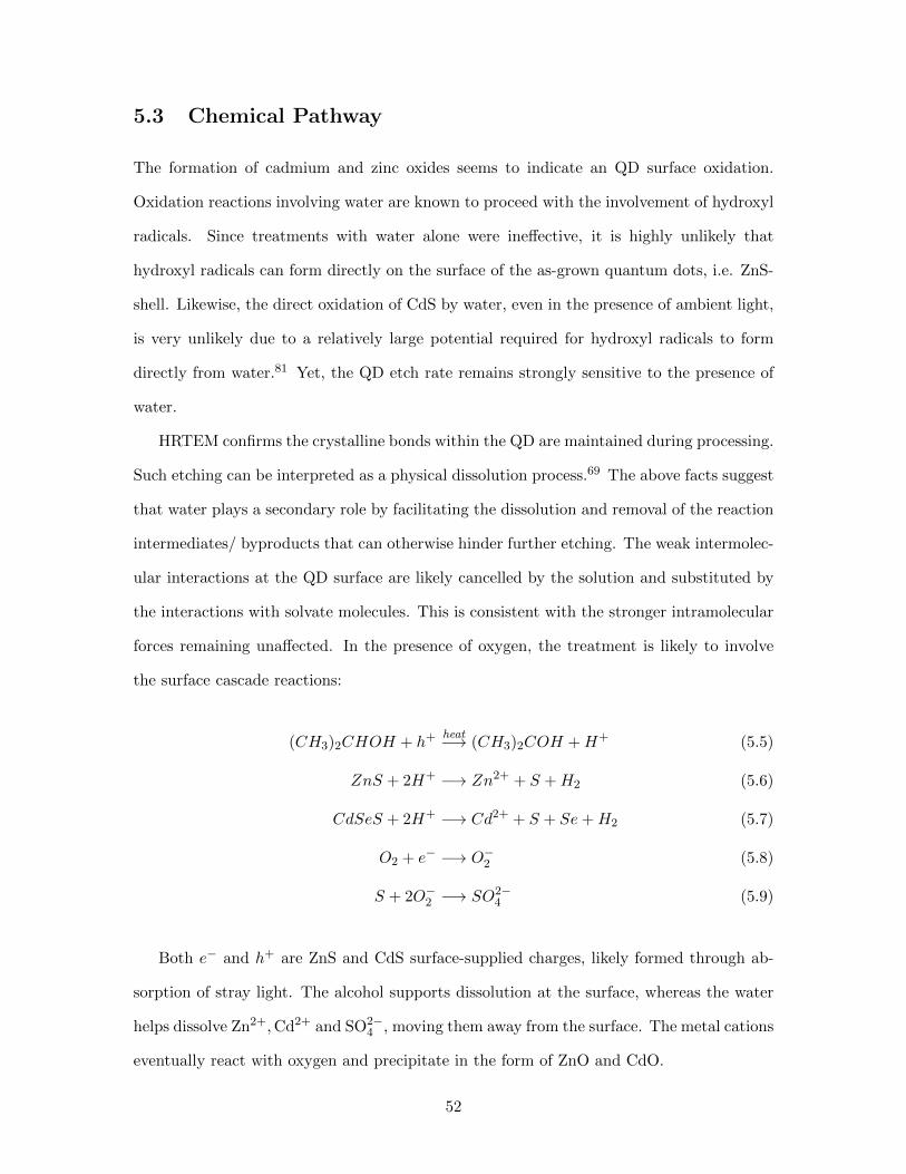
5.3 Chemical Pathway
The formation of cadmium and zinc oxides seems to indicate an QD surface oxidation.
Oxidation reactions involving water are known to proceed with the involvement of hydroxyl
radicals. Since treatments with water alone were ineffective, it is highly unlikely that
hydroxyl radicals can form directly on the surface of the as-grown quantum dots, i.e. ZnS-
shell. Likewise, the direct oxidation of CdS by water, even in the presence of ambient light,
is very unlikely due to a relatively large potential required for hydroxyl radicals to form
directly from water.81 Yet, the QD etch rate remains strongly sensitive to the presence of
water.
HRTEM confirms the crystalline bonds within the QD are maintained during processing.
Such etching can be interpreted as a physical dissolution process.69 The above facts suggest
that water plays a secondary role by facilitating the dissolution and removal of the reaction
intermediates/ byproducts that can otherwise hinder further etching. The weak intermolec-
ular interactions at the QD surface are likely cancelled by the solution and substituted by
the interactions with solvate molecules. This is consistent with the stronger intramolecular
forces remaining unaffected. In the presence of oxygen, the treatment is likely to involve
the surface cascade reactions:
(CH3)2CHOH + h+heat−→ (CH3)2COH +H+ (5.5)
ZnS + 2H+ −→ Zn2+ + S +H2 (5.6)
CdSeS + 2H+ −→ Cd2+ + S + Se+H2 (5.7)
O2 + e− −→ O−2 (5.8)
S + 2O−2 −→ SO2−4 (5.9)
Both e− and h+ are ZnS and CdS surface-supplied charges, likely formed through ab-
sorption of stray light. The alcohol supports dissolution at the surface, whereas the water
helps dissolve Zn2+,Cd2+ and SO2−4 , moving them away from the surface. The metal cations
eventually react with oxygen and precipitate in the form of ZnO and CdO.
52

Chapter 6
Conclusion
6.1 Summary
Colloidal QDs are driving the commercial viability of QD-based technologies. Though
colloidal chemistry methods offer low-cost, high quality quantum dot nanocrystal structures,
it is an additive, one-way technique that results in QDs of a particular size predetermined
during initial synthesis. Additionally, due to Ostwald ripening, synthesis of QDs with
sizes below a certain threshold is not feasible with colloidal methods. For the first time, a
controllable, complimentary down-sizing technique to colloidally grown QDs is reported.
The size and underlying optoelectronic characteristics of the alloyed QDs in II-VI semi-
conductors are manipulated using a top-down approach, achieved by performing alcohol-
based treatments. According to photoluminescence tests, the emission color evolves from
red to green for samples that were treated for up to ∼15 mins through a vapor-based
sonication method. The spectral evolution is found to be consistent with isotropic size re-
duction. Spectroscopic studies are corroborated by HRTEM investigations and, in tandem,
are in strong agreement with the effective mass approximation model. In contrast to prior-
developed top-down semiconductor processing routes, crystallinity, size distribution, and
aspect ratio of QDs remain relatively unaffected throughout the processing. The PL results
exhibit a steady quantum yield once the shell is removed (> 3 min), confirming a minimal
number of defects are created as a side-effect of processing. For the applications requiring
53

high quantum yields, the restoration of the ZnS cap could be considered as a concluding
processing step.
The study presents an technologically viable processing route to achieve post-growth
adjustment to the size and, therefore, the optoelectronic characteristics of core-shell, alloyed
nano-crystals in II-VI semiconductor systems. With this approach, it should be possible
to overcome size limitations due to Ostwald ripening in colloidal synthesis, extending the
emission spectrum and application range of alloyed semiconductor QDs.
6.2 Potential Applications
The most impactful attribute of the reported study is the prospect of post-growth QDs with
down-tunable diameters through facile alcohol treatment. The processing approach herein
could be developed to consistently create previously unobtainable sizes of QDs, unleashing
the potential for many new studies of QDs.
In particular, smaller QDs could be exploited in biomedical applications, by enabling
even smaller size biologically compatible QD-based probes.82–84 In addition to ligand ex-
change, proteins are routinely attached to the shell of the QDs and are used to deploy QDs
to a target site within an in vivo or in vitro specimen.7,8 The core size has a large effect
on the hydrodynamics of the system since the attached protein is comparably small. A
smaller QD would allow for additional penetration schemes into tissues and cells, furthering
the imaging and drug delivery efforts currently underway. For example, the penetration
and accumulation of nanotherapeutics into a tumor cell has been shown to dramatically
increase with the use of 10 nm nanoparticles compared to common 100 nm alternatives.85
A continuation of order-of-magnitude shrinkage could lead to similar drug delivery efficacy
improvements. Furthermore, the ultra-small nanoparticle can more readily pass through
the renal barrier, minimizing in vivo toxicity through renal clearance.
Additionally, it has been shown that the charge injection rate of QD sensitized solar
cells (QDSSC) can be directly attributed to QD size.86 The reported coverage of transport
layer in QDSSCs remains low (< 34%) and could benefit from the deposition of smaller
54

QDs.87 Therefore, integration of smaller QDs could potentially open pathways to better
efficiencies in photovoltaic devices.
The cost of QD manufacturing still stands as a barrier to wide-scale adoption of QD-
based devices. The post-growth size-inflexibility inherent to colloidally grown QDs has yet
to be overcome. Optimized throughput of single-size colloidal QDs would likely drive down
synthesis cost. Through further development of the elementary etching techniques employed
in this study, the potential for bulk QD growth followed by inexpensive processing to control
final size may be achievable.
55

Bibliography
1 A Paul Alivisatos. Perspectives on the Physical Chemistry of Semiconductor Nanocrys-tals. The Journal of Physical Chemistry, 100(31):13226–13239, January 1996.
2 M A Hines and G D Scholes. Colloidal PbS Nanocrystals with Size-Tunable Near-InfraredEmission: Observation of Post-Synthesis Self-Narrowing of the Particle Size Distribution.Advanced Materials, 15(21):1844–1849, November 2003.
3 Al L Efros and M Rosen. The Electronic Structure of Semiconductor NANOCRYSTALS.Annual Review of Materials Research, 30(1):475–521, August 2000.
4 Kyung-Sang Cho, Eun Kyung Lee, Won-Jae Joo, Eunjoo Jang, Tae-Ho Kim, Sang JinLee, Soon-Jae Kwon, Jai Yong Han, Byung-Ki Kim, Byoung Lyong Choi, and Jong MinKim. High-performance crosslinked colloidal quantum-dot light-emitting diodes. NaturePhotonics, 3(6):341–345, May 2009.
5 Future Market Insights. NANOMATERIALS, August 2014.
6 Xiaohu Gao, Yuanyuan Cui, Richard M Levenson, Leland W K Chung, and ShumingNie. In vivo cancer targeting and imaging with semiconductor quantum dots. Naturebiotechnology, 22(8):969–976, August 2004.
7 Igor L Medintz, H Tetsuo Uyeda, Ellen R Goldman, and Hedi Mattoussi. Quantum dotbioconjugates for imaging, labelling and sensing. Nature materials, 4(6):435–446, June2005.
8 Ute Resch-Genger, Markus Grabolle, Sara Cavaliere-Jaricot, Roland Nitschke, andThomas Nann. Quantum dots versus organic dyes as fluorescent labels. Nature methods,5(9):763–775, September 2008.
9 Xiangyou Liu, Gary B Braun, Mingde Qin, Erkki Ruoslahti, and Kazuki N Sugahara. Invivo cation exchange in quantum dots for tumor-specific imaging. Nature Communica-tions, pages 1–12, August 2017.
10 Yasuhiro Shirasaki, Geoffrey J Supran, Moungi G Bawendi, and Vladimir Bulovic. Emer-gence of colloidal quantum-dot light-emitting technologies. Nature Photonics, 7(1):13–23,January 2013.
11 Elise Talgorn, Yunan Gao, Michiel Aerts, Lucas T Kunneman, Juleon M Schins, T JSavenije, Marijn A van Huis, Herre S J van der Zant, Arjan J Houtepen, and LaurensD A Siebbeles. Unity quantum yield of photogenerated charges and band-like transportin quantum-dot solids. Nature Nanotechnology, 6(1):733–739, November 2011.
56

12 Ou Chen, Jing Zhao, Vikash P Chauhan, Jian Cui, Cliff Wong, Daniel K Harris, He Wei,Hee-Sun Han, Dai Fukumura, Rakesh K Jain, and Moungi G Bawendi. Compact high-quality CdSe–CdS core–shell nanocrystals with narrow emission linewidths and sup-pressed blinking. Nature materials, 12(5):445–451, February 2013.
13 J M Caruge, J E Halpert, V Wood, V Bulovic, and M G Bawendi. Colloidal quantum-dot light-emitting diodes with metal-oxide charge transport layers. Nature Photonics,2(4):247–250, March 2008.
14 Hilmi Volkan Demir, Sedat Nizamoglu, Talha Erdem, Evren Mutlugun, Nikolai Gaponik,and Alexander Eychmuller. Quantum dot integrated LEDs using photonic and excitoniccolor conversion. Nano Today, 6(6):632–647, December 2011.
15 Steven A McDonald, Gerasimos Konstantatos, Shiguo Zhang, Paul W Cyr, Ethan J DKlem, Larissa Levina, and Edward H Sargent. Solution-processed PbS quantum dotinfrared photodetectors and photovoltaics. Nature materials, 4(2):138–142, January 2005.
16 Qing Shen, Junya Kobayashi, Lina J Diguna, and Taro Toyoda. Effect of ZnS coating onthe photovoltaic properties of CdSe quantum dot-sensitized solar cells. Journal of AppliedPhysics, 103(8):084304, April 2008.
17 Prashant V Kamat. Quantum Dot Solar Cells. Semiconductor Nanocrystals as LightHarvesters. The Journal of Physical Chemistry C, 112(48):18737–18753, November 2008.
18 Wanli Ma, Joseph M Luther, Haimei Zheng, Yue Wu, and A Paul Alivisatos. Photo-voltaic Devices Employing Ternary PbSxSe1-x Nanocrystals. Nano Letters, 9(4):1699–1703, March 2009.
19 Prashant V Kamat. Quantum Dot Solar Cells. The Next Big Thingin Photovoltaics. TheJournal of Physical Chemistry Letters, 4(6):908–918, March 2013.
20 K W Song, R Costi, and V Bulovic. Electrophoretic Deposition of CdSe/ZnS QuantumDots for Light-Emitting Devices. Wiley Online Library, 2013.
21 F Pelayo Garcıa de Arquer, Ardalan Armin, Paul Meredith, and Edward H Sargent.Solution-processed semiconductors for next-generation photodetectors. Nature ReviewsMaterials, 2(3):13424–16, January 2017.
22 P Michler, A Kiraz, C Becher, W V Schoenfeld, P M Petroff, Lidong Zhang, E Hu,and A Imamoglu. A Quantum Dot Single-Photon Turnstile Device. Science (New York,N.Y.), 290(5500):2282–2285, December 2000.
23 Rudolf Bratschitsch and Alfred Leitenstorfer. Artificial atoms for quantum optics. Naturematerials, 5(11):855–856, November 2006.
24 Robert H Hadfield. Single-photon detectors for optical quantum information applications.Nature Photonics, 3(12):696–705, December 2009.
25 M D Eisaman, J Fan, A Migdall, and S V Polyakov. Invited Review Article: Single-photon sources and detectors. Review of Scientific Instruments, 82(7):071101–26, July2011.
57

26 U.S. E.I.A. Frequently Asked Questions How much electricity is used for lighting in theUnited States? pages 1–2, December 2018.
27 US Department of Energy. LED Efficacy: What America Stands to Gain, October 2017.
28 J R Brodrick. DOE Solid-State Lighting Program, 2015.
29 A I Ekimov and A A Onushchenko. Quantum size effect in three-dimensional microscopicsemiconductor crystals. Journal of Experimental and Theoretical Physics Letters, 34:345–,September 1981.
30 Ch Heyn, A Stemmann, A Schramm, H Welsch, W Hansen, and A Nemcsics. Regimes ofGaAs quantum dot self-assembly by droplet epitaxy. Physical Review B, 76(7):075317,August 2007.
31 V B Verma, M J Stevens, K L Silverman, NL Dias Optics, and 2011. Photon antibunchingfrom a single lithographically defined InGaAs/GaAs quantum dot. osapublishing.org.
32 Andrew Griffiths. Exploring MBE Growth Of Quantum Dots: Low Density Growth ForQuantum Information Devices. 2014.
33 Vitaly Shchukin, Eckehard Scholl, and Peter Kratzer. Thermodynamics and Kinetics ofQuantum Dot Growth. Springer Berlin Heidelberg, Berlin, Heidelberg, 2008.
34 Y Arakawa and H Sakaki. Multidimensional quantum well laser and temperature depen-dence of its threshold current. Applied Physics Letters, 40(11):939–941, August 1998.
35 D Leonard, K Pond, and P M Petroff. Critical layer thickness for self-assembled InAsislands on GaAs. Physical Review B, 50(16):11687–11692, October 1994.
36 Xiaogang Peng, Michael C Schlamp, Andreas V Kadavanich, and A Paul Alivisatos.Epitaxial Growth of Highly Luminescent CdSe/CdS Core/Shell Nanocrystals with Pho-tostability and Electronic Accessibility. Journal of the American Chemical Society,119(30):7019–7029, July 1997.
37 Arto Nurmikko. What future for quantum dot-based light emitters? Nature PublishingGroup, 10(12):1001–1004, December 2015.
38 H T Johnson and L B Freund. Mechanics of coherent and dislocated island morphologiesin strained epitaxial material systems. Journal of Applied Physics, 81(9):6081–6090, June1998.
39 L E Brus. A simple model for the ionization potential, electron affinity, and aqueousredox potentials of small semiconductor crystallites. The Journal of Chemical Physics,79(1):5566–5571, December 1983.
40 L E Brus. Electron-electron and electron-hole interactions in small semiconductor crystal-lites: The size dependence of the lowest excited electronic state. The Journal of ChemicalPhysics, 80(9):4403–4409, May 1984.
41 M G Bawendi, A R Kortan, M L Steigerwald, and L E Brus. X-ray structural char-acterization of larger CdSe semiconductor clusters. The Journal of Chemical Physics,91(1):7282–7290, December 1989.
58

42 A Paul Alivisatos, A L Harris, N J Levinos, M L Steigerwald, and L E Brus. Electronicstates of semiconductor clusters: Homogeneous and inhomogeneous broadening of theoptical spectrum. The Journal of Chemical Physics, 89(7):4001–4011, October 1988.
43 C B Murray, D J Norris, and M G Bawendi. Synthesis and characterization of nearlymonodisperse CdE (E = sulfur, selenium, tellurium) semiconductor nanocrystallites.Journal of the American Chemical Society, 115(19):8706–8715, 1993.
44 C B Murray. Synthesis and characterization of II-VI quantum dots and their assemblyinto 3D quantum dot superlattices. . . . CHEMICAL SOC 1155 16TH ST, September1995.
45 Michael A Boles, Daishun Ling, Taeghwan Hyeon, and Dmitri V Talapin. The surfacescience of nanocrystals. Nature materials, 15(3):364–, March 2016.
46 Irina Lokteva, Nikolay Radychev, Florian Witt, Holger Borchert, Jurgen Parisi, andJoanna Kolny-Olesiak. Surface Treatment of CdSe Nanoparticles for Application in Hy-brid Solar Cells: The Effect of Multiple Ligand Exchange with Pyridine. The Journal ofPhysical Chemistry C, 114(29):12784–12791, June 2010.
47 B O Dabbousi, J Rodriguez-Viejo, F V Mikulec, J R Heine, H Mattoussi, R Ober,K F Jensen, and M G Bawendi. (CdSe)ZnS Core Shell Quantum Dots: Synthesis andCharacterization of a Size Series of Highly Luminescent Nanocrystallites. The Journal ofPhysical Chemistry B, 101(46):9463–9475, November 1997.
48 Margaret A Hines and Philippe Guyot-Sionnest. Synthesis and Characterization ofStrongly Luminescing ZnS-Capped CdSe Nanocrystals. The Journal of Physical Chem-istry, 100(2):468–471, January 1996.
49 Robert E Bailey and Shuming Nie. Alloyed semiconductor quantum dots: tuning theoptical properties without changing the particle size. Journal of the American ChemicalSociety, 125(23):7100–7106, June 2003.
50 Zhengtao Deng, Hao Yan, and Yan Liu. Band Gap Engineering of Quaternary-AlloyedZnCdSSe Quantum Dots via a Facile Phosphine-Free Colloidal Method. Journal of theAmerican Chemical Society, 131(49):17744–17745, November 2009.
51 Tangi Aubert, Marco Cirillo, Stijn Flamee, Rik Van Deun, Holger Lange, Christian Thom-sen, and Zeger Hens. Homogeneously Alloyed CdSe 1– xS xQuantum Dots (0 ≤ x≤ 1): AnEfficient Synthesis for Full Optical Tunability. Chemistry of Materials, 25(12):2388–2390,June 2013.
52 Nguyen T K Thanh, N Maclean, and S Mahiddine. Mechanisms of Nucleation and Growthof Nanoparticles in Solution. ACS Publications, July 2014.
53 Peter Y Yu and Manuel Cardona. Fundamentals of Semiconductors: Physics and Mate-rials Properties, 4th Edition. pages 1–793, April 2010.
54 Su-Huai Wei, S B Zhang, and Alex Zunger. First-principles calculation of band offsets,optical bowings, and defects in CdS, CdSe, CdTe, and their alloys. Journal of AppliedPhysics, 87(3):1304–1311, February 2000.
59

55 Susumu Ninomiya and Sadao Adachi. Optical properties of cubic and hexagonal CdSe.Journal of Applied Physics, 78(7):4681–4689, October 1995.
56 Y S Park and D C Reynolds. Exciton Structure in Photoconductivity of CdS, CdSe, andCdS: Se Single Crystals. Physical Review, 132(6):2450–2457, 1963.
57 Ivan Pelant and Jan Valenta. Luminescence of excitons. Oxford University Press, 2012.
58 A Paul Alivisatos. Semiconductor Clusters, Nanocrystals, and Quantum Dots. Science(New York, N.Y.), 271(5):933–937, February 1996.
59 Jonathan S Steckel, John P Zimmer, Seth Coe Sullivan, Nathan E Stott, Vladimir Bulovic,and Moungi G Bawendi. Blue Luminescence from (CdS)ZnS Core Shell Nanocrystals.Angewandte Chemie International Edition, 43(16):2154–2158, April 2004.
60 Jennifer A Hollingsworth. Semiconductor Nanocrystal Quantum Dots, volume 23. JohnWiley & Sons, Ltd, Chichester, UK, December 2011.
61 M A Baldo, D F O’Brien, Y You, A Shoustikov, S Sibley, M E Thompson, and S R Forrest.Highly efficient phosphorescent emission from organic electroluminescent devices. Nature,395(6698):151–154, September 1998.
62 Wei Wang, Wenliang Feng, Jun Du, Weinan Xue, Linlin Zhang, Leilei Zhao, Yan Li, andXinhua Zhong. Cosensitized Quantum Dot Solar Cells with Conversion Efficiency over12%. Advanced Materials, 30(11):1705746, March 2018.
63 O E Semonin, J M Luther, S Choi, H Y Chen, J Gao, A J Nozik, and M C Beard. PeakExternal Photocurrent Quantum Efficiency Exceeding 100in a Quantum Dot Solar Cell.Science (New York, N.Y.), 334(6062):1530–1533, December 2011.
64 T Edvinsson. Optical quantum confinement and photocatalytic properties in two-,one- and zero-dimensional nanostructures. Royal Society Open Science, 5(9):180387–17,September 2018.
65 K F Riley, M P Hobson, and S J Bence. Mathematical Methods for Physics and Engi-neering. A Comprehensive Guide. Cambridge University Press, March 2006.
66 David J Griffiths. Introduction to Quantum Mechanics. Introduction to quantum me-chanics/ David J. Griffiths. Englewood Cliffs, 1995.
67 Tadd Kippeny, Laura A Swafford, and Sandra J Rosenthal. Semiconductor Nanocrys-tals: A Powerful Visual Aid for Introducing the Particle in a Box. Journal of ChemicalEducation, 79(9):1094–, September 2002.
68 M G Bawendi, M L Steigerwald, and L E Brus. The Quantum Mechanics of Larger Semi-conductor Clusters (”Quantum Dots”). Annual Review of Physical Chemistry, 41(1):477–496, October 1990.
69 Michael Kohler. Etching in Microsystem Technology. Weinheim ; New York : Wiley-VCH,1999.
70 A Henglein. Catalysis of photochemical reactions by colloidal semiconductors. Pure andApplied Chemistry, 56(9):1215–1224, 1984.
60

71 Y Yang Leng. Materials characterization : introduction to microscopic and spectroscopicmethods. Singapore ; Hoboken, NJ : J. Wiley, 2008.
72 Takeshi Aoki. Photoluminescence Spectroscopy. John Wiley & Sons, Inc., Hoboken, NJ,USA, 2012.
73 Horiba. Fluorolog 3 Operation Manual. pages 1–250, October 2002.
74 Th Hahn. International Tables for Crystallography . June 2008.
75 Al L Efros and M Rosen. Quantum size level structure of narrow-gap semiconductornanocrystals: Effect of band coupling. Physical Review B (Condensed Matter and Mate-rials Physics), 58(1):7120–7135, September 1998.
76 James E Bernard and Alex Zunger. Electronic structure of ZnS, ZnSe, ZnTe, and theirpseudobinary alloys. Physical Review B (Condensed Matter), 36(6):3199–3228, August1987.
77 Jianying Ouyang, Christopher I Ratcliffe, David Kingston, Baptiste Wilkinson, JasmijnKuijper, Xiaohua Wu, John A Ripmeester, and Kui Yu. Gradiently Alloyed Zn xCd1-xS Colloidal Photoluminescent Quantum Dots Synthesized via a Noninjection One-PotApproach. The Journal of Physical Chemistry C, 112(13):4908–4919, March 2008.
78 Danielle K Smith, Joseph M Luther, Octavi E Semonin, Arthur J Nozik, and Matthew CBeard. Tuning the Synthesis of Ternary Lead Chalcogenide Quantum Dots by BalancingPrecursor Reactivity. ACS Nano, 5(1):183–190, December 2010.
79 Yow-Jon Lin, Chia-Lung Tsai, Yang-Ming Lu, and Chia-Jyi Liu. Optical and electricalproperties of undoped ZnO films. Journal of Applied Physics, 99(9):093501–5, May 2006.
80 S K Vasheghani Farahani, V Munoz-Sanjose, J Zuniga-Perez, C F McConville, and T DVeal. Temperature dependence of the direct bandgap and transport properties of CdO.Applied Physics Letters, 102(2):022102–5, January 2013.
81 George V Buxton, Clive L Greenstock, W Phillips Helman, and Alberta B Ross. CriticalReview of rate constants for reactions of hydrated electrons, hydrogen atoms and hydroxylradicals (OH/O−)in Aqueous Solution. Journal of Physical and Chemical Reference Data,17(2):513–886, April 1988.
82 Pavel Zrazhevskiy, Mark Sena, and Xiaohu Gao. Designing multifunctional quantum dotsfor bioimaging, detection, and drug delivery. Chem. Soc. Rev., 39(11):4326–29, 2010.
83 Ajmeeta Sangtani, Eleonora Petryayeva, Miao Wu, Kimihiro Susumu, Eunkeu Oh, Alan LHuston, Guillermo Lasarte-Aragones, Igor L Medintz, W Russ Algar, and James BDelehanty. Intracellularly Actuated Quantum Dot–Peptide–Doxorubicin Nanobioconju-gates for Controlled Drug Delivery via the Endocytic Pathway. Bioconjugate Chemistry,29(1):136–148, December 2017.
84 Janet Y Sheung, Pinghua Ge, Sung Jun Lim, Sang Hak Lee, Andrew M Smith, andPaul R Selvin. Structural Contributions to Hydrodynamic Diameter for Quantum DotsOptimized for Live-Cell Single-Molecule Tracking. The Journal of Physical Chemistry C,122(30):17406–17412, July 2018.
61

85 Cliff Wong, Triantafyllos Stylianopoulos, Jian Cui, John Martin, Vikash P Chauhan, WenJiang, Zoran Popovic, Rakesh K Jain, Moungi G Bawendi, and Dai Fukumura. Multi-stage nanoparticle delivery system for deep penetration into tumor tissue. In Proceedingsof the National Academy of Sciences, pages 2426–2431. Department of Chemistry, Mas-sachusetts Institute of Technology, Cambridge, MA 02139, February 2011.
86 Hyeong Jin Yun, Taejong Paik, Benjamin Diroll, Michael E Edley, Jason B Baxter, andChristopher B Murray. Nanocrystal Size-Dependent Efficiency of Quantum Dot SensitizedSolar Cells in the Strongly Coupled CdSe Nanocrystals/TiO 2System. ACS AppliedMaterials & Interfaces, 8(23):14692–14700, June 2016.
87 Zhenxiao Pan, Huashang Rao, Ivan Mora-Sero, Juan Bisquert, and Xinhua Zhong. Quan-tum dot-sensitized solar cells. Chem. Soc. Rev., 47(20):7659–7702, 2018.
62