Tunable fully-differential filter employing MOTA and DACA...
13
Indian Journal of Engineering & Materials Sciences Vol. 23, April & June 2016, pp. 107-119 Tunable fully-differential filter employing MOTA and DACA elements L Langhammer*, J Jerabek, J Polak, R Sotner & P Stork Department of Telecommunication, Faculty of Electrical Engineering and Communication, Brno University of Technology, Technicka 12, 616 00, Brno, Czech Republic Received 16 February 2015; accepted 14 January 2016 A new fully-differential (F-D) filtering structure of the second-order current-mode universal filter is described in this paper. Presented filter is also proposed in a single-ended (S-E) form in order to compare behavior of single-ended and fully-differential structures. Signal-flow graphs method is used to design both presented filters. Multi-output transconductance amplifiers (MOTAs), digitally adjustable current amplifier (DACA), multi-output current follower (MO-CF) and fully differential current follower (FD-CF) are used in proposed filters. Filters possess of ability to adjust their pole frequency and quality factor independently of each other. The actual function of proposed filters has been verified by PSpice simulations and experimental measurements. Keywords: Current amplifiers, Current-mode, DACA, Frequency filter, Fully-differential, MOTA, Single-ended, Operational transconductance amplifier Analogue frequency filters have a wide range of usage in electrical circuitry. We can name branches of industry such as measurement technology, radio- technology, telecommunication, electro-acoustics etc. Lately, we can experience tendency of reducing of the size of integrated circuits in order to decrease energy consumptions leading to decreasing of supply voltage and level of processed signals. This subsequently results in reduction of signal-to-noise ratio and limiting of the dynamic range of the circuit. Therefore, the designers focus also on active elements operating in a current-mode due to advantages which can be achieved in particular cases. The advantages include better signal-to-noise ratio, wider frequency bandwidth, greater dynamic range and lower power consumption 1 . Filters employing different types of current conveyors (CC) can be found for instance in refs. 2-5 Furthermore, it is possible to come across filters using differential voltage current conveyors (DVCC) 6,7 fully-differential current conveyors (FDCC) 8-10 , or differential difference current conveyors (DDCC) 11 . We can mention research of current-mode frequency filters using a variety of amplifiers such as operational transconductance amplifiers (OTA) 12-14 , current differencing transconductance amplifiers (CDTA) 15 , current follower transconductance amplifiers (CFTA) 16-18 and current differential buffered amplifiers (CDBA) 19,20 . Filters employing current followers (CF) can be found for instance in refs. 21-24 Designing of frequency filters can be approached by a multitude of design methods. One of the most common way how to design frequency filters is using autonomous circuit design method 25,26 . Autonomous circuit can be expressed as a circuit of passive and active elements without any excitation source and with no input or output terminals. Such a circuit is purely described by its determinant of admittance matrix which represents the characteristic equation of the analyzed circuit 25 . Subsequently, such circuit can be used as a base element to design various types of frequency filters. The next well-known method used for frequency filter design is synthetic immittance system method 27,28 . Higher-order immittance synthetic elements which consist of serial or parallel combinations of D or E type two-port network can be suitably connected to the circuitry of frequency- dependent voltage or current dividers in order to create filters of the demanded order 27 . We can also mention signal-flow graphs (SFGs) method 13,21 . For the analysis and synthesis of linear electrical networks, Mason-Coates' (M-C) graphs are used. These graphs are formed in the form of nodes and directed branches when variables are represented by nodes and branches define mutual relations between nodes of the analyzed structure. Foremost, a type of —————— *Corresponding author (E-mail: [email protected])
Transcript of Tunable fully-differential filter employing MOTA and DACA...

Indian Journal of Engineering & Materials Sciences Vol. 23, April & June 2016, pp. 107-119
Tunable fully-differential filter employing MOTA and DACA elements
L Langhammer*, J Jerabek, J Polak, R Sotner & P Stork Department of Telecommunication, Faculty of Electrical Engineering and Communication,
Brno University of Technology, Technicka 12, 616 00, Brno, Czech Republic
Received 16 February 2015; accepted 14 January 2016
A new fully-differential (F-D) filtering structure of the second-order current-mode universal filter is described in this paper. Presented filter is also proposed in a single-ended (S-E) form in order to compare behavior of single-ended and fully-differential structures. Signal-flow graphs method is used to design both presented filters. Multi-output transconductance amplifiers (MOTAs), digitally adjustable current amplifier (DACA), multi-output current follower (MO-CF) and fully differential current follower (FD-CF) are used in proposed filters. Filters possess of ability to adjust their pole frequency and quality factor independently of each other. The actual function of proposed filters has been verified by PSpice simulations and experimental measurements.
Keywords: Current amplifiers, Current-mode, DACA, Frequency filter, Fully-differential, MOTA, Single-ended, Operational transconductance amplifier
Analogue frequency filters have a wide range of usage in electrical circuitry. We can name branches of industry such as measurement technology, radio-technology, telecommunication, electro-acoustics etc. Lately, we can experience tendency of reducing of the size of integrated circuits in order to decrease energy consumptions leading to decreasing of supply voltage and level of processed signals. This subsequently results in reduction of signal-to-noise ratio and limiting of the dynamic range of the circuit. Therefore, the designers focus also on active elements operating in a current-mode due to advantages which can be achieved in particular cases. The advantages include better signal-to-noise ratio, wider frequency bandwidth, greater dynamic range and lower power consumption1.
Filters employing different types of current conveyors (CC) can be found for instance in refs.2-5 Furthermore, it is possible to come across filters using differential voltage current conveyors (DVCC)6,7 fully-differential current conveyors (FDCC)8-10, or differential difference current conveyors (DDCC)11. We can mention research of current-mode frequency filters using a variety of amplifiers such as operational transconductance amplifiers (OTA)12-14, current differencing transconductance amplifiers (CDTA)15, current follower transconductance
amplifiers (CFTA)16-18 and current differential buffered amplifiers (CDBA)19,20. Filters employing current followers (CF) can be found for instance in refs.21-24
Designing of frequency filters can be approached by a multitude of design methods. One of the most common way how to design frequency filters is using autonomous circuit design method25,26. Autonomous circuit can be expressed as a circuit of passive and active elements without any excitation source and with no input or output terminals. Such a circuit is purely described by its determinant of admittance matrix which represents the characteristic equation of the analyzed circuit25. Subsequently, such circuit can be used as a base element to design various types of frequency filters. The next well-known method used for frequency filter design is synthetic immittance system method27,28. Higher-order immittance synthetic elements which consist of serial or parallel combinations of D or E type two-port network can be suitably connected to the circuitry of frequency-dependent voltage or current dividers in order to create filters of the demanded order27. We can also mention signal-flow graphs (SFGs) method13,21. For the analysis and synthesis of linear electrical networks, Mason-Coates' (M-C) graphs are used. These graphs are formed in the form of nodes and directed branches when variables are represented by nodes and branches define mutual relations between nodes of the analyzed structure. Foremost, a type of
—————— *Corresponding author (E-mail: [email protected])

INDIAN J. ENG. MATER. SCI., APRIL 2016
108
desired transfer function is determined followed by creation of the M-C graph of the filter according chosen determinant and rules of M-C graphs. Thus, this method represents easy approach to frequency filter design21.
Fully-differential (F-D) structures have some advantages when compared to single-ended (S-E) circuits such as lower harmonic distortion, possibility of greater dynamic range of the processed signal, greater attenuation of common-mode signals and
better power supply rejection ratio. F-D structures have also a few drawbacks that they have more complex design than single-ended structures which leads to larger area taken on the chip and higher power consumption22.
Comparison of the previously reported research2-28 dealing with current-mode filters is given in Table 1. As it can be seen from the table, the proposed filtering structures suffer from one or more of the following drawbacks:
Table 1 – Comparison of the previously reported research
Ref
eren
ce
Yea
r
Num
ber o
f act
ive e
lem
ents
Num
ber o
f pas
sive
elem
ents
Inde
pend
ent t
unin
g o
f f0
Inde
pend
ent t
unin
g o
f Q
Expe
rimen
tal m
easu
rem
ent
Type
of u
sed
activ
e el
emen
t(s)
All
resp
onse
s tak
en fr
om
high
-impe
danc
e out
puts
All
capa
cito
rs g
roun
ded
Tran
sfer
func
tions
F-D
stru
ctur
e
2 2011 2 2 Yes Yes No CCCII Yes Yes All No
3 2012 3 5 Yes Yes No ICCII Yes Yes All No
4 2011 3 7 Yes Partly No MO-CCII Yes Yes All No
5 2009 3 2 Yes Partly No MO-CCCIIs Yes Yes All No
6 2012 3 5 Yes Yes No DVCC Yes Yes All No
7 2003 2 5 Yes Yes No DVCC No Yes All No
8 2012 1 4 Yes Partly No FDCCII Yes Yes All No
9 2009 2 5 Yes Yes No FDCCII Yes Yes H, BP, L No
10 2009 1/1 4/4 Yes Partly No FDCCII No/Yes No/Yes H, BP, L No
11 2014 1 4 Yes Partly No DDCC Yes Yes All No
12 2010 4/5 2/2 Yes Partly No OTA-C Yes Yes All No
13 2011 3 2 Yes Partly Yes CF, OTA Yes Yes All No
14 2009 3 3 Yes Yes Yes OTA Yes Yes All No
15 2009 1 4 Yes Partly No CDTA No Yes H, BP, BS, L No
16 2014 1 3 Yes Partly No CFTA No Yes All No
17 2011 4 2 Yes Yes No CFTA Yes Yes All No
18 2010 1 2 Yes Partly No CCCFTA No Yes All No
19 2008 4 2 Yes Yes No CCCDBA Yes Yes All No
20 2010 3 2 Yes Yes No DO-CCCDBA Yes Yes All No
21 2013 5/6 4/4 Yes Yes No CF, DACA Yes Yes All Yes
22 2013 3/4 4/4 Yes Yes No CF, DACA Yes Yes All (BP) Yes
23 2011 4 2 Yes Yes No CF, DACA Yes Yes All Yes
24 2012 4 4 Yes Yes No CF, DACA Yes Yes All Yes
25 2009 6 3 Yes Yes No CFTA, PCA Yes Yes All No
(Cond.)

LANGHAMMER et al.: TUNABLE FULLY-DIFFERENTIAL FILTER EMPLOYING MOTA AND DACA ELEMENTS
109
Table 2 – Comparison of the previously reported research (Contd.)
Ref
eren
ce
Yea
r
Num
ber o
f ac
tive
elem
ents
Num
ber o
f pa
ssiv
e el
emen
ts In
depe
nden
t tu
ning
o
f f0
Inde
pend
ent
tuni
ng
of Q
Expe
rimen
tal
mea
sure
men
t
Type
of u
sed
activ
e el
emen
t(s)
All
resp
onse
s ta
ken
from
hi
gh-
impe
danc
e ou
tput
s
All
capa
cito
rs
grou
nded
Tran
sfer
fu
nctio
ns
F-D
stru
ctur
e
26 2007 2 3 Yes Yes No OTA No Yes All No 27 2012 1 6 Yes Partly No CCII No No LP No
proposal - 4 2 Yes Yes Yes CF, OTA, DACA
Yes Yes All Yes
CCCII – Second Generation Current-Controlled Conveyor ICCII – Inverting Second Generation Current Conveyor CCII – Second Generation Current Conveyor MO-CCCIIs – Multiple-Output Second Generation Current-Controlled Conveyor DVCC– Differencing Voltage Current Conveyor FDCC – Second Generation Fully-differential Current Conveyor DDCC – Differential Difference Current Conveyor OTA – Operational Transconductance Amplifier CF – Current Follower CDTA – Current Differencing Transonductance Amplifier CFTA – Current Follower Transconductance Amplifier CCCFTA – Current Controlled Current Following Transconductance Amplifier CCCDBA – Current Controlled Current Differencing Buffered Amplifier DO- CCCDBA – Dual-Output Current Controlled Current Differencing Buffered Amplifier DACA – Digitally Adjustable Current Amplifier PCA – Programable Current Amplifier
(i) The quality factor and pole frequency cannot be adjusted independently of each other/or their adjustability is just partly independent4,5,8,10-13,15,16,18,27.
(ii) The structure requires external resistors which leads to greater power consumption and area taken on the chip3,4,6-11,14-16,21-26,27.
(iii) Some of currents responses are not taken from the high-impedance outputs7,10,15,16,18,26,27.
(iv) The structures contain at least one floating capacitor which is not suitable for the implementation and integrability of the circuit10,27.
(v) The filter requires copies of the input currents to obtain particular transfer functions2,5,6,8-12.
(vi) Only structures in refs21-24 are also proposed in the fully-differential form when we can profit from advantages of the F-D structures stated above.
(vii) Additionally, only structures in refs13,14 are supported by experimental measurements of the proposed filters.
Definition of used Active Elements
The designed filters include three types of active elements. The first one is a balanced operational transconductance amplifier (BOTA)13.
Fig. 1 – (a) Schematic symbol of the BOTA, (b) simplified M-C graph of the BOTA, (c) schematic symbol of the multi-output transonductance amplifier, (d) implementation of the MOTA using the UCC-N1B device
Its schematic symbol and simplified M-C graph can be seen in Fig. 1. (a) and (b), respectively. It consists of two balanced inputs and outputs. For our purposes, more output terminals are required especially in case of the F-D structure. Therefore, two more output terminals were added, turning BOTA into a multiple-output transconductance amplifier (MOTA)13. Its schematic symbol is illustrated in
INDIAN J. ENG. MATER. SCI., APRIL 2016
110
Fig. 1 (c). Implementation of the MOTA is shown in Fig. 1 (d) when the universal current conveyor (UCC)29 is used. Resistor R is used to set tranconductance of this element according relation gm = 1/R.
The BOTA element is described by following relation:
),( ININmOUTUTO VVgII … (1)
where gm is the transconductance of this element. The next element is a digitally adjustable current
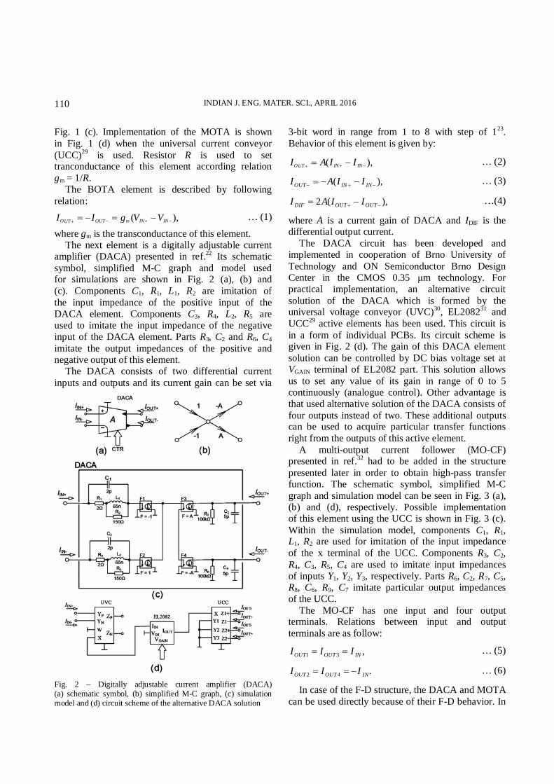
amplifier (DACA) presented in ref.22 Its schematic symbol, simplified M-C graph and model used for simulations are shown in Fig. 2 (a), (b) and (c). Components C1, R1, L1, R2 are imitation of the input impedance of the positive input of the DACA element. Components C3, R4, L2, R5 are used to imitate the input impedance of the negative input of the DACA element. Parts R3, C2 and R6, C4 imitate the output impedances of the positive and negative output of this element.
The DACA consists of two differential current inputs and outputs and its current gain can be set via
3-bit word in range from 1 to 8 with step of 123. Behavior of this element is given by:
),( ININUTO IIAI … (2)
),( ININOUT IIAI … (3)
),(2 OUTOUTDIF IIAI …(4)
where A is a current gain of DACA and IDIF is the differential output current.
The DACA circuit has been developed and implemented in cooperation of Brno University of Technology and ON Semiconductor Brno Design Center in the CMOS 0.35 μm technology. For practical implementation, an alternative circuit solution of the DACA which is formed by the universal voltage conveyor (UVC)30, EL208231 and UCC29 active elements has been used. This circuit is in a form of individual PCBs. Its circuit scheme is given in Fig. 2 (d). The gain of this DACA element solution can be controlled by DC bias voltage set at VGAIN terminal of EL2082 part. This solution allows us to set any value of its gain in range of 0 to 5 continuously (analogue control). Other advantage is that used alternative solution of the DACA consists of four outputs instead of two. These additional outputs can be used to acquire particular transfer functions right from the outputs of this active element.
A multi-output current follower (MO-CF) presented in ref.32 had to be added in the structure presented later in order to obtain high-pass transfer function. The schematic symbol, simplified M-C graph and simulation model can be seen in Fig. 3 (a), (b) and (d), respectively. Possible implementation of this element using the UCC is shown in Fig. 3 (c). Within the simulation model, components C1, R1, L1, R2 are used for imitation of the input impedance of the x terminal of the UCC. Components R3, C2, R4, C3, R5, C4 are used to imitate input impedances of inputs Y1, Y2, Y3, respectively. Parts R6, C2, R7, C5, R8, C6, R9, C7 imitate particular output impedances of the UCC.
The MO-CF has one input and four output terminals. Relations between input and output terminals are as follow:
,31 INOUTOUT III … (5)
.42 INOUTOUT III … (6)
In case of the F-D structure, the DACA and MOTA can be used directly because of their F-D behavior. In
Fig. 2 – Digitally adjustable current amplifier (DACA) (a) schematic symbol, (b) simplified M-C graph, (c) simulation model and (d) circuit scheme of the alternative DACA solution

LANGHAMMER et al.: TUNABLE FULLY-DIFFERENTIAL FILTER EMPLOYING MOTA AND DACA ELEMENTS
111
case of MOCF, the digitally adjustable current amplifier has been used to substitute a F-D current follower. Filter Description
The aim of proposal was to design second-order F-D universal frequency filter working in a current-mode. The next condition was that the filters possess of possibility to adjust their pole frequencies and quality factors independently of each other. The proposed filter is firstly designed in its S-E form in order to compare behavior of the S-E and F-D structure. Single-ended version of the proposed filter includes one MO-CF, two elements of operational transconductance amplifier (BOTA, MOTA) and one DACA element. The circuit structure and simplified M-C graph of this circuit are presented in Fig. 4. The F-D structure of this filter which is shown in Fig. 5 consists of two MOTAs, one DACA and F-D current follower which is constructed by other DACA.
The denominator of transfer functions which is common for both filters is equal to:
.2112212
mmm ggAgsCCCsD … (7)
Fig. 4. S-E structure of the proposed frequency filter: a) scheme, b) simplified M-C graph
Fig. 5 – F-D structure of the proposed frequency filter: (a) scheme, (b) simplified M-C graph and (c) implementation of non-floating capacitances between nodes A and B
Fig. 3 – Multi-output current follower (MOCF) (a) schematic symbol, (b) simplified M-C graph, (c) realization using the UCC-N1B device and (d) simulation model

INDIAN J. ENG. MATER. SCI., APRIL 2016
112
The pole frequency can be adjusted independently of the quality factor of the filter by simultaneous change of transconductances gm1, gm2. Furthermore, the current gain of the DACA allows us to adjust the quality factor of the filter independently of the pole frequency. The pole frequency and quality factor are defined accordingly:
,21
21
210 CC
ggf mm
… (8)
,1
12
21
m
m
gCgC
AQ … (9)
where f0 is the pole frequency, Q is the filter quality factor and parameter A represents the current gain of DACA.
Equations (8) and (9) prove that the pole frequency and quality factor can be adjusted independently. In order to obtain almost the same transfer functions for the F-D filter, factor A has to be replaced by 2A because of the differential gain of the DACA, which is twice higher than in case of S-E structure as it can be seen from Eq. (4). The same applies for gm1, gm2 when their values must be twice higher than in case of S-E transconductances.
The transfer functions of presented filters are represented by:
,2156
Dgg
II
II
I mm
IN
O
IN
OLP … (10)
,1234
DAgsC
II
II
I m
IN
O
IN
OBP … (11)
,212
12
DCCs
II
III
IN
O
IN
OHP … (12)
,21212
1526
DggCCs
III
III
I
mm
IN
OO
IN
OOBS
… (13)
.2112212
145236
DggAgsCCCs
IIII
IIII
I
mmm
IN
OOO
IN
OOOAP
… (14)
Equations (10)-(14) prove that filters are universal because we can obtain all standard transfer functions. It is obvious that all transfer functions correspond
with particular terms of the denominator of proposed filters therefore, they have unity gain in pass-band area regardless values of gm and A parameters (no matching is required for unity gain). Moreover, all transfer functions are taken directly from high-impedance outputs of active elements.
The proposed circuits could be created in CMOS technology in the form of chips for instance. The transistor structure of the DACA and CF elements can be found in ref.22 The transistor structure of the OTA element can be taken for example from ref.33 Tunability of the pole frequency and quality factor of filters would be then controlled by external DC currents (or voltages) set at particular bias terminals. For the practical implementation we have implemented proposed filters in the form of PCBs with individual passive and active elements. The advantage of this autonomous circuit blocks approach is that it is easier to find out if the proposed circuit will be practically functioning correctly and consequently if it is suitable for CMOS implementation in the first place. Similarly with the implementation, using different levels of complexity of simulation models of used active elements we can easily determine how each block affects the proposed circuit as a whole. Used active elements are already implemented on the transistor level in the form of chips, which significantly reduces complexity of PCBs. Simulation and Experimental Results
Simulation and experimental results were carried out to verify appropriate function of proposed filters. Simulations have been performed using PSpice. Models of active elements used for simulation are shown in Figs 2 and 3. Experimental results were performed by measurements of implemented circuits in form of PCBs using a network analyzer Agilent 4395A and V/I, I/V converters. Obtained results were then transferred to a PC using a GPIB bus. Active elements of the proposed filters (OTAs and CFs) were implemented using the UCC-N1B chips connected to the circuits in forms shown in Fig. 1(d) in case of the OTA elements and Fig. 3(c) in case of the CF element. In case of the DACA elements, the alternative circuit solution shown in Fig. 2 (d) has been used. Converters are implemented using integrated circuits OPA86034 and OPA86135. All output responses illustrated in this paper are non-inverting transfer functions.

LANGHAMMER et al.: TUNABLE FULLY-DIFFERENTIAL FILTER EMPLOYING MOTA AND DACA ELEMENTS
113
Specification of values used for simulations and experimental measurements
Following values of specific filter parameters have been chosen for PSpice simulations and experimental measurements: the starting pole frequency f0 = 500 kHz, the starting quality factor Q = 0.707 (Butterworth approximation), values of conductance gm1, gm2 equal to 1 mS, the starting current gain of DACA element has been chosen A = 1. Values of current gain of the F-D filter are half of the values of the S-E structure. As it has been declared above instead of DACA element, an alternative element solution has been used, therefore, values chosen to verify ability to tune the quality factor of proposed filters are solely demonstrational and do not necessary correspond with values which can be obtained by using a real element of the DACA amplifier. The reason why this alternative solution of the DACA element instead of the DACA chip is used is that in case of the F-D we need 4 outputs otherwise it would not be possible to obtain the band-pass transfer function. It would be possible to use a current follower in order to copy and multiply the output signal of the DACA, but that would increase the number of active elements on the PCB. Another advantage is that the quality factor of the filters can tune continuously instead of being limited by discrete steps. Therefore, the proposed filters were simulated and implemented with this circuit instead of the chips. Values of capacitors C1, C2 are calculated according the following relations:
,05.2252 0
11 pF
fQAg
C m
… (15)
.23.4502 0
22 pF
AQfg
C m
… (16)
Hence, for simulations and implementations C1 = 220 pF and C2 = 440 pF have been used. In case of the F-D structure, capacitors have been separated for each branch to avoid using floating elements which is not appropriate for implementation. These capacitors must have twice the values of capacitors used for the S-E filter. Results evaluation
Comparison of simulation and measured output responses of the S-E structure of the proposed filter can be seen in Fig. 6. High-pass transfer function (blue lines) has been taken from output IO2 and the slope of attenuation is 38 dB per decade. Band-pass function (red lines) is taken from IO4 with the slope of 19 dB per decade. Low-pass function (green lines) is taken from output IO6 with 39 dB per decade. Measured functions have slightly lower attenuation than in case of simulated transfer functions. Band-stop transfer function (turquoise lines) has been created by combination of outputs IO2 and IO6. The highest attenuation of this function is at 35 dB in case of simulations and 25 dB of measured function.
Simulated and measured transfer functions of F-D form of the proposed filter are shown in Fig. 7. High-pass transfer function (blue lines) is taken from IO1 with attenuation of 39 dB per decade. In case of band-pass functions (red lines), output IO2 is used and the slope is 20 dB per decade. Low-pass function (green lines) is taken from output IO3 and attenuation is 40 dB per decade. Measured function
Fig. 6 – Comparison of S-E transfer functions high pass, band pass, low pass, band stop simulation (solid lines) and measured functions (dashed lines)

INDIAN J. ENG. MATER. SCI., APRIL 2016
114
of high-pass function have slightly lower attenuation than the simulated function, approximately the same slope in case of band-pass and slightly higher slope for low-pass function. Band-stop transfer function (turquoise lines) has been taken from outputs IO1 and IO3. The highest attenuation is at 47 dB in case of simulations and 35 dB of measured function.
Comparison of experimental measurement of S-E and F-D transfer functions is presented in Fig. 8. From the graph can be seen that F-D transfer functions have slightly higher attenuation than in case of S-E functions, which is mainly given by that the values of conductance used in F-D structures must be twice the values used in case of S-E structures to obtain the same pole frequency. High-pass transfer function of the F-D filter is shifted to higher frequencies, which is also reflected on band-stop function. It can be seen that the filters can be suitably used approximately up to frequency of 6 MHz
because of bandwidth limitations of used active elements. Results are also affected by limitations of used converters. Nevertheless, these results are satisfactory and confirm design correctness and correct operation of both filters.
Possibilities of tuning the pole frequency of proposed S-E and F-D filters are shown if Figs 9-11. For this presentation, low-pass transfer function has been used as an example. Values of parameters gm have been set as gm = (0.5 mS, 1 mS, 1.961 mS) in case of the S-E structure and (1 mS, 2mS, 3.92 mS) in case of the F-D structure. Calculated values of the pole frequency for S-E and F-D structures for chosen values of parameters gm are {255.8 kHz, 511.5 kHz, 1003.0 kHz}. Figure 9 demonstrates possibility of tuning the pole frequency of the proposed S-E filter when simulation and experimental results are compared. Values obtained from simulations are {246.6 kHz, 501.2 kHz, 999.8 kHz} and measured
Fig. 7 – Comparison of F-D transfer functions high pass, band pass, low pass, band stop simulation (solid lines) and measured functions (dashed lines)
Fig. 8 – Comparison of measured S-E (solid lines) and F-D (dashed lines) transfer functions high pass, band pass, low pass, band stop

LANGHAMMER et al.: TUNABLE FULLY-DIFFERENTIAL FILTER EMPLOYING MOTA AND DACA ELEMENTS
115
values are {228.8 kHz, 456.4 kHz, 1085.4 kHz}. From the graph can be seen that gain of measured transfer functions slightly changes when changing values of conductance gm. Results for the F-D filter when simulation and experimental results are compared are shown in Fig. 10. Values obtained from simulations are {251.2 kHz, 505.8 kHz, 1018.6 kHz} and measured values are {259.0 kHz, 525.9 kHz, 1305.4 kHz}. Comparison of S-E and F-D measured transfer functions is illustrated in Fig. 11. Values of the measured pole frequencies can be compared from Table 2. The pole frequencies of the F-D filter are at lower frequencies closer to calculated values than values obtained from the S-E filter. The slopes of attenuation are greater in case of the F-D filter.
Ability of adjusting the quality factor of the proposed filters are presented in Figs 12-14. In this
case, band-pass transfer function has been chosen. Values of the current gain of DACA element have been selected as follows: A = (0.25, 0.5, 1) in case of the S-E filter and (0.125, 0.25, 0.5) in case of the F-D filter. Values of the quality factors calculated for these values of parameter A are {2.83, 1.41, 0.71}.
Comparison of the proposed S-E filter of simulation and experimental results is illustrated in Fig. 12. Values of obtained quality factors are {0.73, 1.49, 3.08} in case of simulation and {0.67, 1.39, 3.26} for measured results. Figure 13 shows comparison of the F-D filter when simulation and experimental results are compared. The quality factors obtained from simulations are {0.71, 1.41, 2.87} and {0.91, 2.02, 3.42}. Comparison of S-E and F-D measured results is presented in Fig. 14. Values of measured pole frequencies can be compared in Table 3. From Table 2, it can be seen that measured
Fig. 9 – Demonstration of possibility of adjusting the pole frequency of the S-E filter: simulation (solid lines) and experimental measurement (dashed lines)
Fig. 10 – Demonstration of possibility of adjusting the pole frequency of the F-D filter: simulation (solid lines) and experimental measurement (dashed lines)

INDIAN J. ENG. MATER. SCI., APRIL 2016
116
values of the quality factor of the F-D structure are significantly higher than expected values. Also the pole frequency in case of the F-D structure is shifting when the quality factor changes.
Differences between simulated and measured results at higher frequencies are mainly given by bandwidth limitations of used real active elements and also by limitations of used converters. The measured results are also affected by input/output impedances (they are not low/high enough) of the active elements in the structure. The input impedance of the DACA element is the most dominant parasitic element at higher frequencies.
The dynamic range of the proposed implemented S-E (red line) and F-D (green line) filter is illustrated in Fig. 15. For this matter, measurement of the DC transfer function of the all-pass filters has been carried out. Measurement has been set from -3 mA to 3 mA with 5 uA step and it has been carried out using current source Agilent B2902A and multimeters Agilent 34410A. From the graph it can be seen that the dynamic range of the F-D filter is significantly greater than the dynamic range of the S-E filter. Furthermore, the dynamic range of the S-E filter has its bottom limit at 0.81 mA when the upper limit is 0.55 mA. In case of the F-D filter it is 1.3 mA for the upper limit and 1.1 mA for the bottom limit.
The PCB implementation of the proposed S-E filter including the UCC chips is shown in Fig. 16. Figure 17 shows the PCB implementation of the proposed F-D filter also including the UCC chips.
Fig. 11 – Comparison of possibility of adjusting the pole frequency when comparing experimental results: S-E filter (solid lines), F-D filter (dashed lines)
Fig. 12 – Demonstration of possibility of adjusting the quality factor of the S-E filter: simulation (solid lines) and experimental measurement (dashed lines)
Table 2 – Comparison of measured pole frequencies (kHz)
Conductance (S-E/F-D) 0.5/1 mS 1/2 mS 1.961/3.922 mS
Calculated 255.8 511.5 1003.0 S-E filter 228.8 456.4 1085.4 F-D filter 259.0 525.9 1305.4

LANGHAMMER et al.: TUNABLE FULLY-DIFFERENTIAL FILTER EMPLOYING MOTA AND DACA ELEMENTS
117
Table 3 – Comparison of measured quality factors Gain A (S-E/F-D) 0.25/0.125 0.5/0.25 1/0.5
Calculated 2.83 1.41 0.71 S-E filter 3.26 1.39 0.67 F-D filter 3.42 2.02 0.91
A chip of the DACA element (each chip includes two DACA elements, in this case DACA elements designated as no. 5 and 6) and its alternative circuit solution are illustrated in Fig. 18.
Fig. 13 – Demonstration of possibility of adjusting the quality factor of the F-D filter: simulation (solid lines) and experimental measurement (dashed lines)
Fig. 14 – Comparison of possibility of adjusting the quality factor when comparing experimental results: S-E filter (solid lines), F-D filter (dashed lines)

INDIAN J. ENG. MATER. SCI., APRIL 2016
118
Fig. 15 – Comparison of the dynamic range of proposed filters (experimental results): S-E filter (red line), F-D filter (green line)
Fig. 16 – PCB of the proposed S-E filter (top side)
Fig. 17 – PCB of the proposed F-D filter (top side)
Fig. 18 – DACA element: chip (right), alternative circuit solution of the DACA element (left) Conclusions
An actual function of proposed filters has been verified by simulation and also by experimental measurements. From relations (10)-(14) can be seen that the S-E and F-D proposed filters are universal because we can obtain all transfer functions. Furthermore, all transfer functions match the particular term of the denominator therefore, they have the unity gain in pass-band area regardless the values of gm and A parameters. Ability of adjusting the pole frequency and quality factor of proposed filters has been discussed. Comparing the S-E and F-D structure, transfer functions of the F-D structure possess of greater attenuation and the pole frequencies of this

LANGHAMMER et al.: TUNABLE FULLY-DIFFERENTIAL FILTER EMPLOYING MOTA AND DACA ELEMENTS
119
filter are closer to calculated values. The quality factors of the S-E filter are closer to calculated values when quality factors of the F-D filter are significantly higher than expected and the pole frequency is slightly shifting when the quality factor changes.
Acknowledgement Research described in the paper was supported by
the National Sustainability Program under grant LO1401. For the research, infrastructure of the SIX Center was used.
References 1 Tomazou C, Lidgey F J & Haigh D G, Analog IC design: the
current-mode approach (Institution of Electrical Engineers, London) 1996, 646.
2 Kumngern M, J Electr Electron Eng Res, 3(9) (2011) 162-170.
3 Chen H, Int J Circuits Theor Appl, 42(4) (2012) 376-393. 4 Horng J W, Indian J Eng Mater Sci, 17(3) (2010) 169-174. 5 Chen H P & Chu P L, IEICE Electron Express, 6(2) (2009)
122-128. 6 Chen H, AEU-Int J Electron Commun, 66(4) (2012) 332-339. 7 Temizyurek C & Myderrizi I, Current-Mode Universal Filter
Implemented with DVCCs, in Proc. Int Conf on Electrical and Electronics Engineering, Bursa, Turkey, December 2003, 3-7.
8 Chen H, Wang S, Li P, Chou N & Chang C H, Single FDCCII-based current-mode universal biquadratic filter, in Proc. 2nd Int Conf on Consumer Electronics, Communications and Networks (CECNet), Yichang, China, 21-23 April 2012, 2076 - 2079.
9 Gür F & Anday F, Analog Integrated Circuits Signal Process, 60(3) (2009) 231-236.
10 Kaçar F, Metin B, Kuntman H & Cicekoglu O, Current-Mode Multifunction Filters Using a Single FDCCII, in Proc Int Conf on Electrical and Electronics Engineering ELECO , Bursa, Turkey, 2009, II-54-II-57.
11 Horng J W, Wu C M & Herencsar N, Indian J Pure Appl Phys, 52, (2014), 556-562.
12 Lee C H, Circuits, Syst Signal Process, 29(2) (2010) 263-274. 13 Jerabek J, Sotner R & Vrba K, J Electr Eng, 62(6) (2011)
317-326. 14 Sotner R, Petrzela J & Slezak J, Radioengineering, 18(3)
(2009) 285-294. 15 Prasad D, Bhaskar D R & Singh A K, AEU - Int J Electron
Commun, 63(6) (2009) 497-501. 16 Tangsrirat W, Indian J Eng Mater Sci, 17(2) (2010)
99-104. 17 Tangsrirat W, AEÜ-Int J Electron Commun, 65 (2011) 783-
787. 18 Herencsar N, Koton J, Vrba K, Lahiri A & Cicekoglu O,
Current-Controlled CFTA-Based Current-Mode SITO
Universal Filter and Quadrature Oscillator, in Proc Int Conf on Applied Electronics (AE), Pilsen, Czech Republic, 8-9 September 2010, 1-4.
19 Tsukutani T, Sumi Y & Yabuki N, Electronically tunable current-mode universal biquadratic filter using CCCDBAs, in Proc Int Symp on Intelligent Signal Processing and Communications Systems ISPACS, Bangkok, Thailand, 6-8 December 2008, 1 - 4.
20 Siripruchyanun M & Jaikla W, Int J Circuit Theory Appl, 38(3) (2010) 321-330.
21 Langhammer L & Jerabek J, Int J Adv Telecommun, Electrotech, Signals Syst, 3(1) (2014) 1-12.
22 Jerabek J, Koton J, Sotner R & Vrba K, Analog Integrated Circuits Signal Process, 74(1) (2013) 129-139.
23 Jerabek J, Vrba K & Jelinek M, in Proc Int Conf on Applied Electronics, Pilsen, Czech Republic, 2011, 189-192.
24 Jerabek J & Vrba K, Comparison of the Fully-Differential and Single-Ended Solutions of the Frequency Filter with Current Followers and Adjustable Current Amplifier, in Proc 11th Int Conf on Networks ICN, Reunion, France, 2012, 50-54.
25 Herencsar N, Koton J, Vrba K, Lattenberg I & Misurec J, Telfor J, 1(2) (2009) 49-52.
26 Herencsar N & Vrba K, IEICE Electrons Express, 4(21) (2007) 650-656.
27 Brandstetter P & Klein L, Design of Frequency Filters by Method of Synthetic Immittance Elements with Current Conveyors, in Proc Int Conf Applied Electronics (AE), Pilsen, Czech Republic, 9-11 September 2012, 37-40.
28 Jerabek J & Vrba K, Design of Fully-Differential Filters with nth-order Synthetic Elements and Comparison with Single-Ended Solution, in Proc 3rd Int Conf on Communication Software and Networks (ICCSN), Xi'an, China, 27-29 May 2011, 437-441.
29 Sponar R & Vrba K, Int J Comput Sci Network Security, 3A(6) (2006) 57-63.
30 Herencsar N, Koton J, Jerabek J, Vrba K & Cicekoglu O, Radioengineering, 20(1) (2011) 10-18.
31 EL2082 - Current-mode Multiplier (datasheet). Online, <http://html.alldatasheet.com/html-pdf/59879/ELANTEC/EL2082/245/1/EL2082.html>
32 Jerabek J, Sotner R & Vrba K, Comparison of the SITO Current-Mode Universal Filters Using Multiple- Output Current Followers, in Proc 35th Int Conf on Telecommunications and Signal Processing, Prague, Czech Republic, 3-4 July 2012, 406-410.
33 Biolek D, Biolková V & Kolka Z, Int J Electron, Circuits Syst, 1(4) (2007) 214.
34 Texas Instruments - OPA860 - Wide Bandwidth Operational Transconductance Amplifier (datasheet). Online, <http://www.ti.com/lit/ds/symlink/opa860.pdf>
35 Texas Instruments - OPA861 - Wide Bandwidth Operational Transconductance Amplifier (datasheet). Online, http://www.ti.com/lit/ds/symlink/opa861.pdf