TTL Logic Databook TexasInstruments
56
The TTL Data Book General Information N
-
Upload
zeca-vieira -
Category
Documents
-
view
76 -
download
8
Transcript of TTL Logic Databook TexasInstruments

The TTL Data Book
General Information N

Contents
Title Page
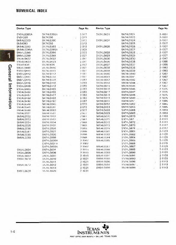
D NUMERICAL INDEX 1-3
FUNCTIONAL INDEX 1-7
GLOSSARY 1-39
EXPLANATION OF FUNCTION TABLES 1-43
PARAMETER MEASUREMENT INFORMATION 1-45
TYPICAL CHARACTERISTICS 1-51
uoR
eLuJ
oim
i iw
aueD
1 -2

Device Type Page No. Device Type Page No.
SN 5400 SN7400 2-3 SN54S30 SN74S30 2-127 SN54LSOO SN74LSOO 2-3 SN54LS31 SN74LS31 • 2-133 SN54S00 SN74S00 2-3 SN5432 SN7432 • 2-137 SN5401 SN7401 2-9 SN54LS32 SN74LS32 2-137 SN54LSO1 SN74LSO1 2-9 SN54S32 SN74S32 . .. 2-137 SN 5402 SN7402 2-13 SN5433 SN7433 ....... 2-143 SN54LSO2 SN74LSO2 . 2-13 SN54LS33 SN74LS33 2 - 143 SN54S02 SN74S02 . .. 2-13 SN5437 SN7437 . 2-147 SN5403 SN7403 . 2-19 SN54LS37 SN74LS37 . 2-147 SN54LSO3 SN74LSO3 2-19 SN54S37 SN74S37 2-147 SN54S03 SN74S03 .. 2-19 SN5438 SN7438 . . . . 2-153 SN5404 SN7404 2-25 SN54LS38 SN74LS38 2-153 SN54LSO4 SN74LSO4 2-25 SN54S38 SN74S38 2-153 SN54SO4 SN74SO4 . . . 2-25 SN5439 SN7439 2.159 SN5405 SN7405 . 2-31 SN5440 SN7440 2-161 SN54LS05 SN74LSO5 .. 2-31 SN54LS40 SN74LS40 . . . . 2-161 SN54S05 SN74S05 2-31 SN54S40 SN74S40 . 2-161 SN5406 SN7406 . 2-37 SN5442A SN7442A 2-167 SN 5407 SN7407 2-39 SN54LS42 SN74LS42 2-167 SN5408 SN7408 . 2-41 SN5445 SN7445 .. 2-173 SN54LSO8 SN74LSO8 2-41 SN5446A SN7446A 2-175 SN54S08 SN74S08 2-41 SN5447A SN7447A . 2-175 SN5409 SN7409 2-47 SN54LS47 SN74LS47 2.175 SN54LSO9 SN74LSO9 2-47 SN5448 SN7448 . 2-175 SN54S09 SN74S09 2-47 SN54LS48 SN74LS48 2-175 SN5410 SN7410 2-53 SN54LS49 SN74LS49 2-175 SN54LS10 SN74LS10 2-53 SN5450 SN7450 2-189 SN54S10 SN74S10 2-53 SN5451 SN7451 2-193 SN54LS11 SN74LS11 2.59 SN54LS51 SN74LS51 2-193 SN54S11 SN74S11 2-59 SN54S51 SN74S51 2.193 SN5412 SN7412 2-63 SN5453 SN7453 . 2-199 SN54LS12 SN74LS12 2-63 SN5454 SN7454 2-201 SN5413 SN7413 .. 2-67 SN54LS54 SN74LS54 2-201 SN54LS13 SN74LS13 2-67 SN54LS55 SN74LS55 2-205 SN5414 SN7414 . 2-77 SN54LS56 SN74LS56 2-207 SN54LS14 SN74LS14 .. 2-77 SN54LS57 SN74LS57 2-207 SN54LS15 SN74LS15 2.87 SN54S64 SN74S64 2.211 SN54515 SN74S15 2.87 SN54S65 SN74S65 2-211 SN5416 SN7416 .. 2-37 SN54LS68 SN74LS68 2-215 SN5417 SN7417 2-39 SN54LS69 SN74LS69 2-215
SN74LS19A 2-91 SN5470 SN7470 2-221 SN 5420 SN7420 2-95 SN5472 SN7472 . 2-225 SN54LS20 SN74LS20 2-95 SN5473 SN7473 .. . 2-229 SN54S20 SN74S20 . 2-95 SN54LS73A SN74LS73A 2-229 SN54LS21 SN74LS21 2.101 SN5474 SN7474 2-235 SN5422 SN7422 2.105 SN54LS74A SN74LS74A 2.235 SN54LS22 SN74LS22 .. 2-105 SN54S74 SN74S74 2-235 SN54S22 SN74S22 2-105 SN5475 SN7475 2-241 SN 5423 SN7423 2-111 SN54LS75 SN74LS75 2-241
SN74LS24A 2-91 SN5476 SN7476 2-247 SN5425 SN7425 2-111 SN54LS76A SN74LS76A 2-247 SN 5426 SN7426 . 2-115 SN5477 2-241 SN54LS26 SN74LS26 . 2-115 SN54LS77 2.241 SN5427 SN7427 2-119 SN54LS78A SN74LS78A 2.253 SN54LS27 SN74LS27 2-119 SN5483A SN7483A 2-257 SN5428 SN7528 2-123 SN54LS83A SN74LS83A 2-257 SN54LS28 SN74LS28 2-123 SN5485 SN7485 2-263 SN 5430 SN7430 2-127 SN54LS85 SN74LS85 2-263 SN54LS30 SN74LS30 2-127 SN54S85 SN74S85 2-263
Ge
ne
ral In
form
ati
on
NUMERICAL INDEX
TEXAS INSTRUMENTS 1 -3
POST OFFICE BOX 655012 • DALLAS. TEXAS 75265

Device Type Page No. Device Type Page No.
SN5486 SN7486 2-271 31454143 SN74143 2-439 SN54LS86A SN74LS86A 2 271 SN54145 SN74145 2.447 SN54S86 SN74S86 2-271 3N541.S145 SN74LS145 2-447 SN5490A SN7490A 2-271 SN54147 SN74147 2-451 SN54LS90 SN74LS90 2-277 SN54LS147 SN74LS147 . . 2-451 SN5491A SN7491A 2-289 3354148 SN74148 2-451 SN54LS91 SN74LS91 2 289 3N54L.S148 SN74LS148 2-451 SN5492A SN7492A 2 277 3354150 SN74150 2-457 SN54LS92 SN74LS92 2 277 33541510 SN74151A 2-457 SN5493A SN7493A 2-277 SN54LS151 SN74LS151 2-457 SN54LS93 SN74LS93 2-277 SN54S151 SN74S151 2 457 SN5494 SN7494 2-293 5554153 SN74153 2-465 SN5495A SN7495A 2-297 SN54LS153 SN74LS153 2-465 SN54LS95B SN74LS958 2 297 3N5-1S153 SN74S153 2 465 SN5496 537496 2-305 3354154 5374154 2 471 SN54LS96 SN74LS96 2 305 SN54155 5374155 2-475 SN5497 SN7497 2 311 SN54LS155A SN74LS155A 2-475 SN54107 SN74107 .. 2-319 SN54156 SN74156 2-475 SN54LS107A SN74LS107A . 2-319 SN54LS156 SN74LS156 2-475 SN54109 3374109 2 325 5354157 SN74157 2-483 SN54LS109A SN74LS109A 2-325 SN54LS157 SN74LS157 2-483 SN54111 SN74111 2-331 SN54S157 SN74S157 . 2-483 SN54LS112A SN74LS112A 2-335 3N54LS158 SN74LS158 2 483 SN54S112 511745112 2-335 51\1545158 SN74S158 2-483 SN54LS113A SN74LS113A 2-343 31\154159 SN74159 2-489 SN54S113 SN74S113 2-343 SN54160 SN74160 2-493 SN54LS114A SN74LS114A 2-349 9N541.S160A SN74LS1600 2-493 SN54S114 SN74S114 2-349 5354161 SN74161 2-493 SN54116 SN74116 2-357 3N5455161A SN74LS161A 2-493 SN54120 SN74120 2-361 3354152 SN74162 2 493 SN54121 SN74121 2 367 SN54LS162A SN74LS162A 2-493 SN54122 SN74122 2-373 SN54S162 SN74S162 2-493 SN54LS122 SN74LS122 2-373 3554163 9N174163 2-493 SN54123 3N74123 2 373 SN54LS163A SN74LS163A 2-493 SN54LS123 SN74LS123 2-373 33545163 SN74S163 2-493 SN54S124 SN74S124 2 383 SN54164 SN74164 2-515 SN54125 SN74125 2 387 535453164 SN74LS164 2-515 SN54LS125A SN74LS125A 2-387 5354165 SN74165 2-521 SN54126 SN74126 2 387 SN54LS165A SN74LS165A 2-521 SN54L5126A SN74LS126A . 2-387 SN54166 SN74166 . 2-529 SN54128 SN74128 2-393 SN54LS166A SN74LS166A 2 529 SN54130 SN74130 2-373 SN54167 SN74167 2-537 SN54132 SN74132 2-395 3N154L916913 SN74LS1698 2-543 SN54LS132 SN74LS132 2 395 53545169 SN74S169 2-543
SN54S132 SN74S132 2 395 5354170 SN74170 2-555 SN54S133 93746133 2 407 53541.5170 SN74LS170 2-555 SN54S134 SN74S134 2 -111 33541.5171 SN74LS171 2-565
SN54S135 SN74S135 2-415 SN74172 2-569 SN54136 SN74136 2-417 5354173 5374173 . 2-575
SN54LS136 SN74LS136 2-417 3N54L5173A SN74LS173A 2-575 SN54LS137 SN74LS137 2 421 5354171 5N74174 2-581 SN54LS138 SN74LS138 2-425 SN54LS174 SN74LS174 2-581 SN54S138 SN74S138A 2-425 SN54S174 SN74S174 2-581 SN54LS139A SN74LS139A 2-431 3354175 SN74175 2-581
SN54S139 SN74S139A 2-431 3N54LS175 SN74LS175 2-581 SN54S140 SN74S140 2-435 SN543175 SN74S175 2-581
uop,e
wio
lui
NUMERICAL INDEX
1 - 4 TEXAS
INSTRUMENTS

1
Ge
ner
al In
form
ati
on
NUMERICAL INDEX
Device Type Page No. Device Type Page No.
SN54176 SN74176 2-587 SN54LS266 SN74LS266 2-757 SN54177 SN74177 2 587 SN54273 SN74273 2-759 SN54178 SN74178 2-593 SN54LS273 SN74LS273 2-759 SN54180 SN74180 2-597 SN54276 SN74276 2-763 SN54LS181 SN74LS181 2-601 SN54278 SN74278 2 767
SN54S181 SN745181 ....... .. .. 2-601 SN54279 SN74279 2-771 SN54S182 SN74S182 2-611 SN54LS279A SN74LS279A . 2-771 SN54LS183 SN74LS183 2-617 SN54LS280 SN74LS280 2-775 SN54190 SN74190 2-619 SN54S280 SN74S280 ... 2-775 SN54LS190 SN74LS190 2-619 SN54283 SN74283 2 781 SN54191 SN74191 2-619 SN54LS283 SN74LS283 2-781
SN54LS191 SN74LS191 2-619 SN54S283 SN74S283 2-781
SN54192 SN74192 2-633 SN54284 SN74284 2-787 SN54LS192 SN74LS192 2-633 5N54285 SN74285 2-787 SN54193 SN74193 2-633 SN54290 SN74290 2 791 SN54LS193 SN74LS193 2-633 5N54L5290 SN74LS290 2-791 SN54194 91174194 2-645 SN54LS292 SN74LS292 2 799 SN54LS194A SN74LS194A 2-645 SN54293 SN74293 2-791 SN54S194 SN74S194 2-645 SN54LS293 SN74LS293 2-791 SN54195 SN74195 2-655 SN54LS294 SN74LS294 2-799 SN54LS195A SN74LS195A 2-655 SN54LS2958 SN74LS295B 2-807 SN54S195 SN74S195 2-663 SN54LS297 SN74LS297 2-811 SN54196 SN74196 2-663 SN54298 SN74298 2-817 SN54LS196 SN74LS196 2-663 SN54LS298 SN74LS298 . 2-817 SN54S196 SN74S196 2-663 SN54LS299 SN74LS299 2-823 SN54197 SN74197 2-663 SN54S299 SN74S299 2-823 SN54LS197 SN74LS197 2-663 SN54LS320 SN74LS320 2-829 SN54S197 SN74S197 . 2-663 SN54LS321 SN74LS321 . 2 829 SN54198 SN74198 2-671 SN54LS322A SN74LS322A 2-835 SN54199 SN74199 2-671 SN54ALS323 SN74ALS323 2-841 SN54221 SN74221 2-681 SN54LS348 SN74LS348 2-845 SN54LS221 SN74LS221 2-681 SN54S350 SN74S350 2-849 SN54LS240 SN74LS240 2-691 SN54LS352 SN74LS352 2-855 SN54S240 SN74S240 2-691 SN54L5353 SN74LS353 2-859 SN54LS241 SN74LS241 2-691 SN54LS354 SN74LS354 2-863 SN54S241 SN74S241 2-691 SN54LS355 SN74LS355 2-863 SN54LS242 SN74LS242 2-697 SN54LS356 SN74LS356 2-863 SN54LS243 SN74LS243 2-697 SN54365A SN74365A 2-873 SN54LS244 SN74LS244 2-691 SN54LS365A SN74LS365A 2-873 SN54S244 SN74S244 2-691 SN54366A SN74366A 2-873 SN54LS245 SN74LS245 2-701 SN54LS366A SN74LS366A 2-873 SN54246 SN74246 2-705 SN54367A SN74367A 2-873 SN54247 SN74247 2-705 SN54LS367A SN74LS367A 2 873 SN54LS247 SN74LS247 2-705 SN54368A SN74368A 2-873 SN54LS248 SN74LS248 2-705 SN54LS368A SN74LS368A 2-873 SN54251 SN74251 2-715 SN54LS373 SN74LS373 2-883 SN54LS251 SN74LS251 2-715 SN54S373 SN74S373 2-883 SN54S251 SN74S251 2-715 SN54LS374 SN74LS374 2-883 SN54LS253 SN74LS253 2-723 SN54S374 SN74S374 2-883 SN54S253 SN74S253 2-723 SN54LS375 SN74LS375 2 891 SN54LS25713 SN74LS257B 2 729 SN54376 SN74376 2 893 SN54S257 SN74S257 2-729 SN54LS377 SN74LS377 2-895 5N54LS2586 SN74LS2586 2-729 SN54LS378 SN74LS378 2-895 SN54S258 SN74S258 2-729 SN54LS379 SN74LS379 2-895 SN54259 SN74259 2-735 SN54LS381A SN74LS381A 2-899 SN54LS2598 SN74LS2598 2-735 SN54S381 SN74S381 2-899 SN54S260 SN74S260 2-739 SN54L5382 SN74LS382 2 899 SN54LS261 SN74LS261 2-743 SN54LS384 SN74LS384 2 907 SN54265 SN74265 2-751 SN54LS385 SN74LS385 2-913
TEXAS INSTRUMENTS
4
6
1-5
POST OFFICE BOX 655012 • DALLAS. TEXAS 75265
NUMERICAL INDEX
Device Type
SN54LS386A
SN54390
SN54LS390
SN54393
SN54LS393
MI/SN54LS395A
SN54LS396
. 5N54LS399
SN54LS422
. SN54LS423
SN54S436
SN54LS440
SN54LS441
SN54LS442
SN54LS444
SN54LS445
SN54LS446
SN54L5449
SN54LS465
SNE4LS466
SN54LS467
SN54LS468
SN54LS490
SN54LS540
SN54LS541
SN54LS590
SN54LS591
SN54LS592
SN54LS593
SN54LS594
SN54LS595
SN54LS596
SN54LS597
SN54LS598
SN54L5599
SN54LS604
SN54LS606
SN54LS607
SN54LS610
SN54LS612
SN54LS620
Page No. Device Type Page No.
SN74LS386A 2-917 SN54LS621 SN74LS621 2-1031 SN74390 . . . 2-919 SN74LS623 2-1031 SN74LS390 2-919 SN 54 LS624 SN74LS624 .. 2-1037 SN74393 2-919 SN74LS625 2-1037 SN74LS393 2-919 SN54LS626 SN74LS626 . . . 2-1037 SN74LS395A 2-929 SN74L8627 2-1037 SN74LS396 2-933 SN54LS628 SN74LS628 . . 2-1037 SN74LS399 2-937 SN54LS629 SN74LS629 2-1037 SN74LS422 2-941 SN54LS630 SN74LS630 2-1047
SN74LS423 2-941 SN54LS636 SN74LS636 2-1055 SN74S436 2-947 SN54LS637 SN74LS637 2-1055 SN74LS440 2-951 SN54LS638 SN74LS638 2-1063
SN74LS441 2-951 SN54LS639 SN74LS639 2-1063
SN74LS442 2-951 SN54LS640 SN74LS640 2-1067 SN74 LS444 2-951 SN54LS641 SN74LS641 2-1067 SN74LS445 2-957 SN54LS642 SN74LS642 2-1067
SN74LS446 2-959 SN54LS644 SN74LS644 .. 2-1067
SN74LS449 2-959 SN54LS645 SN74LS645 2-1067 SN74LS465 2-963 SN54LS646 SN74LS646 2-1075
SN74LS466 2-963 SN54LS647 SN74LS647 2-1075 SN74LS467 2-963 SN54 LS648 SN74L5648 . 2-1075 SN74 LS468 2-963 SN54LS649 SN74LS649 2-1075
SN74LS490 2-967 SN54LS651 SN74LS651 2-1085
SN74LS540 2-973 SN54LS652 SN74LS652 2-1085
SN74LS541 2-973 SN54LS653 SN74LS653 2-1085 SN74LS590 2-977 SN54LS668 SN74LS668 . 2-1093
SN74LS591 2-977 SN54LS669 SN74LS669 . 2-1093
SN74L5592 2-981 SN54LS670 3N74L3670 2-1103 SN74LS593 2-981 SN54LS671 SN74LS671 . 2-1111
SN74LS594 2-989 SN54LS672 SN74LS672 .. 2-1111
SN74LS595 2-993 SN54 LS673 SN74LS673 2-1117
SN74LS596 2-993 SN54LS674 SN74LS674 . . . 2-1117
SN74LS597 2-999 SN54LS681 SN74LS681 2-1123
SN74LS598 2-999 SN54LS682 SN74LS682 2-1129
SN74LS599 2-989 SN54LS684 SN74LS684 2-1129
SN74LS600A 2-1007 SN54LS685 SN74LS685 2-1129
SN74LS601A 2-1007 SN74LS686 2-1129
SN74LS603A 2-1007 SN54LS687 SN74LS687 2-1129
SN74LS604 2-1015 SN54LS688 SN74LS688 2-1129
SN74LS606 2-1015 SN54LS690 SN74LS690 2-1139
SN74LS607 2-1015 SN54LS691 SN74LS691 2-1139
SN74LS610 2-1021 SN54LS693 SN74LS693 2-1139
SN74 LS611 2-1021 SN54LS696 SN74LS696 2-1149
SN74LS612 2-1021 SN54LS697 SN74LS697 . 2-1149
SN74LS613 2-1021 SN54LS699 SN74LS699 .. 2-1149
SN74 LS620 2-1031
uoR
ewa
olui
lei
auaD
1-6 TEXAS
INSTRUMENTS 4
POST OFFICE BOO 655012 • DALLAS, TEXAS 75265

FUNCTIONAL INDEX
Column heading Literature Number provides the latest available technical source for a particular product.
TI's technical literature is identified by a seven- or eight-character product source code consisting of four 141 alpha characters, three 131 numeric characters, and a revision letter, if applicable. If the fourth alpha character is an "S", then the document is a stand-alone data sheet, e.g., SDAS106A. The code is printed
at the upper right-hand corner on the front cover and the lower left-hand corner on the back cover of a
data book, and at the lower left-hand corner on the back page of a data sheet.
List of Applicable Databooks:
SCAD001 A = Advanced CMOS Logic Databook SCLD001B = High-Speed CMOS Logic Databook
SDADOO1B = ALS/AS Logic Databook
SDFD001 = F Logic Databook
SDLD001A = Standard TTL Logic Databook
SDVD001 = LSI Logic Databook
SDZDOO1 B = Programmable Logic Databook
Gen
era
l In
form
atio
n
TEXAS INSTRUMENTS
POST OFFICE BOX 655012 • DALLAS, TEXAS 75265
1-7
FUNCTIONAL INDEX uog
ewaolu
i le
aau
a9
GATES
POSITIVE-NAND GATES
DESCRIPTION TYPE
TECHNOLOGY LITERATURE
NUMBER STD
TTL LS S ALS AS F HC AC ACT
8-Input '30
• • • sill rInnl A
A • : ' ••B
• ..,... '9
• SD: '
'11030 • • SC.. • •1A
13-Input '133
• SD'• 'B
• SC IB
• -. IA
12-Input '134 • 'A
Dual 2-Input '8003 • SDADOO1B
Dual 4-Input
'13 • • SDLD001A
20
• • • SDI. I 'A
A • SD/ I • 113
• • i • ' • '
40 A '.300113
• • • )001A
'1020 A SD! 'I3
'11020 • • SC!. A
Triple 3-Input
10
• • • SDLD001A
• • SDAD001B
• I )001B
• )001
'1010 A SD: • IB
'11010 • • SC •1 • 'A
Quad 2-input
00
A • SDAD001B
• • • SD 'A
• SC • i B
• SDI '
'26 • • SDI 'A
'37 • • • SDI .A
A SD! • 1B
38 • • • SDI • IA
A SDA.,.....71B
'39 • grIl 0001A
'132 • • • •.• )001A
• .. )001B
'5 A A '•00018
'1: • • : )001A
Hex 2-Input '804
A B SDAD0018
• SC IR
'1804 A •
• . Denotes available technology.
♦ = Denotes planned new.
A = Denotes "A" suffix available in the technology indicated.
B . Denotes "B" suffix available in the technology indicated.
TBA Denotes information To Be Announced.
TEXAS INSTRUMENTS
POST OFFICE BOX 655012 • DALLAS TEXAS 75265
1-s

DESCRIPTION TYPE
TECHNOLOGY LITERATURE
NUMBER STD
TTL LS S ALS AS F HC AC ACT
Dual 4-Input '22 • • SDLD001A
B SDAD00113
Triple 3-Input '12 • • SDLD001A
A SDAD00113
Quad 2-Input
'01 • • SDLD001A
• SDAD001 B • )001B
'03
• • • )001A
B 'D0018
• )001B
'1003 A SDAD00113
POSITIVE-AND GATES WITH OPEN-COLLECTOR OUTPUTS
DESCRIPTION TYPE
TECHNOLOGY LITERATURE
NUMBER STD
TTL LS S ALS AS F HC AC ACT
Triple 3-Input '15 • • SDLD001A
A SDADOO1B
Quad 2-Input '09
• • • SDLD001A
• SDA0001B
• SCLD001B
• SDFD001
Quad Schmitt '7001 • SCLD001B
Gen
eral In
form
ati
on
FUNCTIONAL INDEX
POSITIVE-NAND GATES WITH OPEN-COLLECTOR OUTPUTS
• = Denotes available technology.
♦ Denotes planned new.
A Denotes "A" suffix available in the technology indicated. B Denotes "B" suffix available in the technology indicated. TBA = Denotes information To Be Announced.
TEXAS INSTRUMENTS
POST OFFICE 80X 855012 • DALLAS. TEXAS 75265
1-9

FUNCTIONAL INDEX u
og
etw
om
IM
MO
POSITIVE -AND GATES
DESCRIPTION TYPE
TECHNOLOGY LITERATURE
NUMBER STD
TTL LS S ALS AS F HC AC ACT
Dual 4-Input '21
A • SDATIRR18
• SD' 'A
• SC B
• SD • • •
'11021 • • SC' lA
Triple 3-Input
11
• • SDI. A
A • SD/ 1B
• 'B
•
'1011 A soapon , R
'11011 • • • S CAT ", _
Quad 2-Input
08
• • • , ... • • ......A...J01B
• SCLD0018
• SDFD001
'1008 A A SDAD001 B
'11008 • • SCADOO1A
POSITIVE-OR GATES
DESCRIPTION TYPE
TECHNOLOGY LITERATURE
NUMBER STD
TTL LS S ALS AS F HC AC ACT
Triple 3-Input '4075 • SCLD001B
Quad 2- Input
32 '
• • • SDLDO01A
• • SDAD001 B • • B
• .
A A gilt!, D0018
• • 10018
'11032 • • .,Apoo 1 A
Hex 2-Input 832
A B SDAD001 B
• SCLD001B
'1832 A • SDADOO1B
• Denotes available technology.
♦ Denotes planned new.
A Denotes "A" suffix available in the technology Indicated.
B Denotes "B" suffix available in the technology indicated.
TBA Denotes information To Be Announced.
TEXAS INSTRUMENTS
POST OFFICE sox 655012 • DALLAS, TEXAS 75265
1-10

FUNCTIONAL INDEX
POSITIVE-NAND GATES
DESCRIPTION TYPE
TECHNOLOGY LITERATURE
NUMBER STD
TTL LS S ALS AS F HC AC ACT
Dual 4-Input
with Strobe '25 • SDLD001A
Dual 4-Input '4002 • SCLD0018
Dual 5-Input '260 • SDL0001A
Triple 3-Input 27
• • SDLD001A
• • SDA000113 —
• SCLC ' -
• SDK
'11027 • • SCAD001 A
Quad 2-Input
'02
• • • SDLD00 I A
• • '8
• i 'B
• )001
28 • • .. )001A
A SDAD001B
'33 • • SDLDOO1A
A SDAD00113
'36 • SCLD001B
• SDFD001
'1002 A SDAD001B
A SDAD0018
'7002 • SC B
'11002 • • SC ' 1 A
Hex 2-Input '805
A B
• ' B
'1805 A • SDAD00113
POSITIVE-OR/NOR GATES
DESCRIPTION TYPE
TECHNOLOGY LITERATURE
NUMBER STD
TTL LS S ALS AS
I F HC j AC ACT
8-Input '4078 [ A I_ SCLD001B
• -= Denotes available technology.
♦ = Denotes planned new
A = Denotes "A" suffix available in the technology indicated
B = Denotes "B" suffix available in the technology indicated.
TBA = Denotes information To Be Announced.
TExAs INSTRUMENTS
POST OFFICE BOX 655012 • DALLAS, TEXAS 75265

FUNCTIONAL INDEX u
og
eiw
olu
i IR
JO
UG
D
1-12
EXCLUSIVE-OR/-NOR GATES
DESCRIPTION TYPE
TECHNOLOGY LITERATURE
NUMBER STD
TTL LS S ALS AS HC
Quad 2-Input
Exclusive-OR
Gates with
Totem-Pole Outputs
'86
• A • qn , O001A
• _ • •
. .
• • • — SCLD001 B
Quad 2-Input
Exclusive-OR
Gates with Open-
Collector Outputs
'136
• • SDLD001A
• —
— ♦ SDAD001B
Quad 2-Input
Exclusive-NOR
Gates
'266 • SDI Iloo1A
•
'810 • ♦ S..' 113
'7266 • SCLD001B
Quad 2-Input
Exclusive-NOR
Gates with Open-
Collector Outputs
'811 • ♦ SDADOO1B
Quad Exclusive-
OR/-NOR Gates '135 • SDLD001A
AND-NOR GATES
DESCRIPTION TYPE
TECHNOLOGY LITERATURE
NUMBER STD
TTL LS S ALS AS HC HCT
2-Wide 4-Input '55 •
SDLD001A
4-Wide 4-2-3-2
Input '64 •
4-Wide 2-2-3-2
Input '54 • •
Dual 2-Wide
2-Input '51
• • •
• SCLD001B
AND-NOR GATES WITH OPEN-COLLECTOR OUTPUTS
DESCRIPTION TYPE
TECHNOLOGY LITERATURE
NUMBER STD
TTL LS S ALS AS HC HCT
4-Wide 4-2-3-2-
Input '65 • SDLD001A
• m- Denotes available technology.
• Denotes planned new.
A Denotes "A" suffix available in the technology indicated.
B m Denotes "B" suffix available in the technology indicated.
TBA Denotes information To Be Announced.
TEXAS INSTRUMENTS
POST OFFICE BOX 665012 • DALLAS, TEXAS 75265
40

Gen
eral In
form
ati
on
FUNCTIONAL INDEX
EXPANDABLE GATES
DESCRIPTION TYPE
TECHNOLOGY LITERATURE
NUMBER STD
TTL LS S ALS AS HC HCT
Dual 2-Wide
AND-OR-Invert '50 •
SDLD001A Dual 4-Input
Positive-NOR
with Strobe
'23 •
MULTIFUNCTION GATES AND ELEMENTS
DESCRIPTION TYPE
TECHNOLOGY LITERATURE
NUMBER STD
TTL LS S ALS AS HC HCT
Inverter,3-/4-
Input NAND/NOR
Combination
'7006 • SCLD001B
6-Section NAND
Invert, NOR '7008 • SC LD001B
Quadruple
Complimentary
Output Logic
Element
'265 • SDLD001A
DELAY ELEMENTS
DESCRIPTION TYPE
TECHNOLOGY LITERATURE
NUMBER STD
TTL LS S ALS AS HC HCT
Inverting and
Noninverting
Elements 2-Input
NAND-Buffer
31 • SDLD001A
• = Denotes available technology.
♦ = Denotes planned new.
A = Denotes "A" suffix available in the technology indicated. B Denotes "B" suffix available in the technology indicated.
TBA = Denotes information To Be Announced.
TEXAS 444/1 INSTRUMENTS 1-13
POST OFFICE BOX 655012 • DALLAS, TEXAS 75265

FUNCTIONAL INDEX uo
Rew
aNui
lea
eueD
INVERTERS/NONINVERTINI; BUFFERS
HEX INVERTERS/NONINVERTERS
DESCRIPTION TYPE
TECHNOLOGY LITERATURE
NUMBER STD
TTL LS S ALS AS F HC AC ACT HCU
Hex Inverters
'04
• • • A B • ..a. A • I B
• SCI.' ' B • SCI B
• SDFD001 '11004 • • SCAD001A
'05 • • • SDLD001A
A crlArinnt B
• '06 • ,.r•I ".. 'A
'14 • • . 'A
• •B '16 • SDLD001A '19 • SDLD001A
'1004 • A SDADOO1B '1005 • SDAD001B
Hex
Noninverter
'34 • • SDAD001B '11034 • • SCADOO1A
• Denotes available technology.
• Denotes planned new.
A Denotes "A ' suffix available in the technology indicated.
• Denotes "B" suffix available in the technology indicated.
TBA = Denotes information To Be Announced.
1-14 TrxAs INSI RI IMENTS
POST OFFICE BOX 655012 • DALLAS, TEXAS 75265

Gen
eral In
form
atio
n
FUNCTIONAL INDEX
DRIVER AND BUS TRANSCEIVERS
HEX DRIVERS
DESCRIPTION TYPE
TECHNOLOGY LITERATURE
NUMBER STD
TTL LS S ALS AS HC HCT
Hex 2-Input
Driver
'808 A B - - )001B
• )001 B
'1808 A • SDAD00113
Hex Driver
'07 • SDLD001A
'17 •
'1R, A SDADOO1B
. • A SDADOO1B _ . • SDADOO1B
Noninverting
Hex Buffers/
Drivers
' 365 A A )001A
• )001B
'366 A A SDLD001A
• SCLD001B
'367 A A SDLD001A
• SCLD001B
'368 A A SDLD001A
• SCLD001B
DRIVERS WITH OPEN-COLLECTOR OUTPUTS
DESCRIPTION TYPE
TECHNOLOGY LITERATURE
NUMBER STD
TTL LS S ALS AS HC HCT
Noninverting
Octal Buffers,
Drivers
'757 • SDADOO1B
760 •
SDADOO1B •
Inverting
Octal Buffers,
Drivers
'756 • • SDADOO1B
'763 • • SDADOO1B
Inverting and
Noninverting
Octal Buffers,
Drivers
'762 5 SDADOO1B
• = Denotes available technology.
• . Denotes planned new.
A Denotes "A" suffix available in the technology indicated.
B . Denotes "B" suffix available in the technology indicated.
TBA . Denotes information To Be Announced.
TEXAS IN STRU M ENTS
POST OFFICE BOX 655012 • DALLAS TEXAS I
4 1 - 1 5

FUNCTIONAL INDEX U
OR
BIL
UN
LII I
MIB
UO
D
1-16
BUS TRANSCEIVERS WITH OPEN-COLLECTOR OUTPUTS
DESCRIPTION TYPE
TECHNOLOGY LITERATURE
NUMBER STD
TTL LS S ALS AS F HC
Noninverting
Quad
Transceivers
'759 • SDAD00113
Inverting Quad
Transceivers '758 • • SDADOO1B
12-mA/24-mA/
40-mA Sink
Transceivers
'615 • SDAD0018
'621
A • SDA0001B
• )001A
• • )001
'639 A • CllAIVIO113
•
641 A • .....
• SC 'A
12-mA/24-mA/
48-mA Sink
Inverting Output
Transceivers
'614 • SC•• 18
'622 A • crlArinn .1 B
•
'638 A •
• SLDLOO1A
'642 A • SDAD0018
• SDLD001A
'653 • ' •1B
• A
12-mA/24-rnA/
48-mA Sink, True
and Inverting
Output Transceivers
'644
A • SDAD00113
• SDLD001A
Registered with
Multiplexed
12-mA/24-mA/
48-mA True
Output Transceivers
'647 A • SDADOO1B
• SDLD001A
'654 • SDLD001A
• SDV0001
Registered with
Multiplexed
12-mA/24-mA/
48-mA Inverting
Output Transceivers
'649
• SDLD001A
• SDVD001
• = Denotes available technology .
• m Denotes planned new.
A m Denotes "A" suffix available in the technology indicated.
B Denotes "B" suffix available in the technology indicated.
TBA Denotes information To Be Announced.
TEXAS 49/ INSTRUMENTS
POST OFFICE BOX 655012 • DALLAS, TEXAS 75265

DESCRIPTION TYPE TECHNOLOGY
LITERATURE NUMBER
STD TTL
LS S ALS AS F HC HCT AC ACT BCT
Quad Buffers/ Drivers with Independent Output Controls
'125 • A • • 'A
• 'B
'126 • A )01A
• • • )01B
Noninverting Octal Buffers/ Drivers
'241
• • SDLD001A B • SDADOO1B
• • SCLD00113 • crwrIont
• ••
'11241 • •
'244
• • SDLD001A B • SDADOO1B
• • qcl 0001B • • • '
• • '11244 • • SCADOO1A
'465 • SDLD001A
A SDAD0016
'467 A SDADOO1B
• SDLD001A
'541
• • -101A • ,......A,...J01B
S • SCLD001B '1244 A SDADOO1B
1
Gen
era
l In
form
ati
on
FUNCTIONAL INDEX
DRIVERS WITH 3-STATE OUTPUTS
• Denotes available technology.
• Denotes planned new,
A Denotes "A" suffix available in the technology indicated.
B Denotes "B" suffix available in the technology indicated.
TBA Denotes information To Be Announced.
TEXAS Ail INSTRUMENTS
POST OFFICE BOX 655012 • DALLAS. TEXAS 75265
1-17

uop,
ewaN
ui p
eieu
eD
FUNCTIONAL INDEX
DRIVERS WITH 3-STATE OUTPUTS (continued)
DESCRIPTION TYPE
TECHNOLOGY LITERATURE
NUMBER STD
TTL LS S ALS AS F HC HCT AC ACT BCT
Inverting Octal
Buffers/Drivers
'231 • • SDAD001B
'240
• • SDLD001A A • SDAD001B
• • )001B • )001
• ;004 '11240 • • )001A
'466 • 1001A
A ' )001 B
'468 A SDADOO1B
• SDLD001A
'540
• SDLD001A
• SDADOO1B • • E 'B
'1240 • E.....,, 1B
Inverting and
Noninverting
Octal Buffers/
Drivers
'230 • SDADOO1B
Noninverting
10-Bit Buffers/
Drivers
'2827 • SCLS051
'29827 • SDVD001
• SCLS052
Inverting 10-Bit
Buffers/Drivers
'2828 • SCLS051
'29828 • SOVD001
• SCLS052
• Denotes ava lable technology.
• . Denotes planned new.
A Denotes "A" suffix available in the technology indicated.
B Denotes "B" suffix available in the technology indicated.
TBA Denotes information To Be Announced.
1-18 TEXAS 11"01/
INSINSTRUMENTS POST OFFICE 000 655012 • DALLAS, TEXAS 75205

FUNCTIONAL INDEX
BUS TRANSCEIVERS WITH 3-STATE OUTPUTS
DESCRIPTION TYPE TECHNOLOGY LITERATURE
Nt VI l it LS S ALS AS F HC HCT AC ACT BCT
Noninverting
Quad
Transceivers
'243
• SDLI 1 A • SDADOO1B
• • SCLD001B
• SDFD001
Inverting Quad
Transceivers
'242
• SDLD001A
B • SDADOO1B • • SCLD0016
• SDFD001
'1242 • SDADOO1B
Quad
Tridirectional
Transceivers
'442 • SDL0001A
Octal
Transceivers
'245
• SDLD001A
A • SDAD0018 • • SCLD00113
• SDFD001
♦ TBA '11245 • • SCAD001A
'620
• • SCLD001B
A • SDAD003 • SD
• SC '11620 ♦ ♦ SCAD001A
'640
• • SCLD001B
A • SDADOO1B • SDLD001A
'11640 ♦ • SCAD001A
'643
• • SCLD001B A • SDADOO1B
• SDLD001A '11643 • • SCAD001A
'1245 A SDAD001A
♦ TBA
• . Denotes available technology.
♦ Denotes planned new.
A Denotes "A" suffix available in the technology indicated
B Denotes "B" suffix available in the technology indicated.
TBA Denotes information To Be Announced.
TEXNS INSTRUMENTS
POST OFFICE BOX 655012 • DALLAS, TEXAS 75265
4
Ge
ner
al In
form
ati
on
1-19

FUNCTIONAL INDEX U
OR
BLU
JOW
I leiG
UO
D
1-20
BUS TRANSCEIVERS WITH 3-STATE OUTPUTS (continued)
DESCRIPTION TYPE TECHNOLOGY LITERATURE NUMBER LS S ALS AS F HC HCT AC ACT BCT
Octal Bus Transceivers with Registers
'543 • SDFD001 '544 • SDFD001
'646 • • SCL B
• • SDI. 1B • SD A
648 • • SC B
• • SD' • • ' B • SD . • • A
'651 • • SCLD001B
• • SDADOO1B • SDLD001A
'652 • • SCLD001B
• • SDAD001B • SDLD001A
'11646 • •
SCADOO1A '11648 • • '11651 • • '11652 • •
8-/9-Bit Bus
Transceivers
with Parity
Checker/ Generator
'658 • •
S '659 • • '664 • •
CLD001B
'665 • •
'29833 • SDAS119A
• SCBS003
'29834 • SDAS119A
• SCBS003
'29853 • 3118
• 3002
'29854 • SDAS118
• SCBS002
• Denotes available technology.
♦ _== Denotes planned new
A Denotes "A" suffix available in the technology indicated
B Denotes "B" suffix available in the technology indicated.
TBA Denotes information To Be Announced.
TEXAS 40 INSTRUMENTS
POST OFFICE BOX 655012 • DALLAS. TEXAS 75265

Ge
ne
ral I
nfo
rma
tio
n
FUNCTIONAL INDEX
BUS TRANSCEIVERS WITH 3-STATE OUTPUTS (continued)
DESCRIPTION TYPE TECHNOLOGY LITERATURE
NUMBER LS S ALS AS F HC HCT AC ACT BCT
Noninverting 9-
Bit Transceivers '29863
• SD iA
• SC
Inverting 9-Bit
Transceivers 29864
• SDAS096A
♦ TBA
Noninverting 10-
Bit Transceivers '29861
• SDAS097
• SCLS056 Inverting 10-Bit
Transceivers 29862
• SDAS097
♦ TBA
12-mA/24-mA/
48-mA Sink,
True Output
Transceivers
'623
A • SDADOO1B • SDLD001A
• • SCLD001B
• )001
'645
• • )001B
A • 1B
• A
'654 • SDADOO1B
• SDLD001A
'1640 A SDAD0018
'1645 A
'1' ♦ ♦ SCAD001A Universal
Transceiver/
Port Controllers
. •
SDAD00113 '856 •
'877 •
• m Denotes ava lable technology.
♦ Denotes planned new.
A -= Denotes "A" suffix available in the technology indicated.
B m Denotes "B" suffix available in the technology indicated.
TBA Denotes information To Be Announced.
TEXAS INSTRUMENTS
POST OFFICE BOX 655012 • DALLAS. TEXAS 75265
4 1-21

FUNCTIONAL INDEX u
oRet
woiL
ii IW
OU
G9
LINE DRIVERS/BUS TRANSCEIVERS/MOS DRIVERS
DESCRIPTION TYPE
TECHNOLOGY LITERATURE
NUMBER STD
TTL LS S ALS AS HC BCT
Bus
Transceivers
'2242 •
SDAD001E1
•
. •.
'2640 •
'2645 •
Line
Drivers
'2240 •
'2240 •
TBA '2241 •
'2244 •
'2244 •
'2540 • SDA0001B
'2541 •
LINE DRIVERS
DESCRIPTION TYPE
TECHNOLOGY LITERATURE
NUMBER STD
TTL LS S ALS AS HC HCT
Octal Buffers
AND/Line Drivers
with Input
Pull up
Resistors
'746 •
SDADOO1B
'747 •
Octal/Line
Dnvers.'wyth
3-State Output
'2540 •
"2541 •
• Denotes available technology.
• . Denotes planned new.
A Denotes "A" suffix available in the technology indicated.
B Denotes "B" suffix available in the technology indicated.
TBA = Denotes information To Be Announced.
1-22 TEXAS INSTRUMENTS
POST LJL ,CE HD% 1S5012 • DAL L

DESCRIPTION TYPE
TECHNOLOGY LITERATURE
NUMBER STD
TTL LS S ALS AS HC HCT
Quad 2-Input
Positive-NOR '128 •
SDLD001A Dual 4-Input
Positive-NAND '140 •
Hex 2-Input
Positive-NAND
'804 A B SDADOO1B
• SCLD001B
'1804 A • SDADOO1B
Hex 2-Input
Positive-NOR
'805 A B
• SCLD001B
'1805 A • SDADOO1B
Hex 2-Input
Positive-AND
'808 A B
• SCLD001B
'1808 A • SDADOO1B
Hex 2-Input
Positive-OR
'832 A B
SCLD001 13 •
'1832 A • SDAD0018
MULTIFUNCTION DRIVERS Gen
era
l In
form
ati
on
FUNCTIONAL INDEX
50-OHM/75-OHM LINE DRIVERS
DESCRIPTION TYPE
TECHNOLOGY LITERATURE
NUMBER STD
TTL LS S ALS AS HC HCT
Dual Pulse
Synchronizers/
Drivers
'120 • SDLD001 A
• . Denotes available technology.
• Denotes planned new.
A Denotes "A" suffix available in the technology indicated.
B . Denotes "B" suffix available in the technology indicated.
TBA Denotes information To Be Announced.
TEXAS INSTRUMENTS 1-23
POST OFFICE BOX 655012 • DALLAS, TEXAS 75265

DESCRIPTION TYPE
TECHNOLOGY LITERATURE
NUMBER STD
TTL LS S ALS AS HC AC ACT F
Dual J-K Edge-Triggered
'73 • A .. • !A
• 'B
'76 • A SDLD001A
• SCLD001B
78 • A SDLD001A
• SCLD001B
107 • A SDLD001A
• SCLD001B
109
• A SDLD001A A • SDADOO1B
• SCLD001B • SDFD001
'112
A A sni ilnni A
A • SC. --' 8
• SD. • '
'113
A A SD • • 'A A SDADOO1B
• sci 0001B
• ' )001
'114
A A 1001A A SDADOO1B
• SC A 00018 • . Inn .1
'11109 • •
Single J-K Edge- Triggered
70 • SDL0001A
Dual D-Type 74
• A • A • ' )001B
• • 10018 • SDFD001
'11074 • • SCADOO1A
Dual D-Type with 2-Input NAND/NOR Gates
'7074 • SCLD001B '7075 •
'7076 •
Dual 4-Bit D-Type Edge-Triggered
'874 B •
SDAD001B 876 A •
'878 A •
'879 A •
uop
etw
om
lea
gue°
FUNCTIONAL INDEX
FLIP-FLOPS
DUAL AND SINGLE FLIP-FLOPS
1 -24
• m Denotes available technology.
• m Denotes planned new.
A Denotes "A" suffix available in the technology indicated.
B Denotes "B" suffix available in the technology indicated.
TBA Denotes information To Be Announced.
TEXAS AP INSTRUMENTS
POST OFFICE BOX 655012 • DALLAS. TEXAS 75265
Gen
eral In
form
ati
on
FUNCTIONAL INDEX
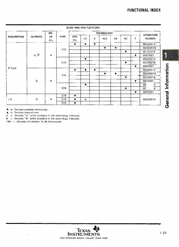
QUAD AND HEX FLIP-FLOPS
DESCRIPTION OUTPUTS NO. OF
FFs
TYPE TECHNOLOGY
LITERATURE NUMBER
STD
TTL LS S ALS AS HC F
D-Type
Q, iri 4
175
• • • SDLD001A • • SDAD001 B
• SCLD001B
• SDFD001
'379 • SDLD001A
• SCLD001B • SDFD001
Q 6
'174
• • • SDLD001A • • SDAD001B
• SCLD001B • SDFD001
'378 • SD A
• SC B
• SDFD001
J-K a 4
'276 • SDLD001A '279 • A
'376 •
• Denotes available technology. • Denotes planned new. A = Denotes "A" suffix available in the technology indicated, • Denotes "B" suffix available in the technology indicated. TBA Denotes information To Be Announced.
TEXAS 1/0 INSTRUMENTS
POST OFFICE SOX 856012 • DALLAS, TEXAS 75265
1-25

uoR
euu
olui
le.
lau
aD
FUNCTIONAL INDEX
1 -26
OCTAL, 9-BIT, AND 10-BIT D•TYPE FLIP-FLOPS
DESCRIPTION NO. OF
BITS OUTPUTS TYPE
TECHNOLOGY LITERATURE
NUMBER STD LS S ALS AS HC HCT AC ACT BCT F
True Data
Octal
3-State
'374
• • SDLD001A • • SDADOO1B
• • SCLD001B
♦ TBA
• SDFD001
'574
A • ' )OO1B • • )0018
• • • •001
'11374 • • ' )001A
True Data with
Clear
2-State '273
• • SDLD001A
• SDAD00113
• SCLD001B
• SDFD001
3-State
'575 A •
SDADOO1B '874 A •
'878 A •
True with
Enable 2-State '377
• )001A • )001B
• SDFD001
Inverting 3-State
'534
• • SD 'B
• • SC B
• -
•
• 001
'564
A SDADOO1B
• • SCLD001B
• SDFD001
'576 A • SDAD001B
'826 • SDAD00113
'11534 • • SCAD001A
Inverting with
Clear 3-State
'577 A •
SDADOO1B '879 A •
Inverting with
Preset 3-State '876 A •
True
'825 • SDAD0018
9-Bit 3-State
'823 • •
'1823 • SDAS126
Inverting 3-State '824 • SDAD0018
True 10-Bit
3-State '821 •
'1821 • SDAS131
Inverting 3-State '822 • SDAD001B
• . Denotes available technology.
• Denotes planned new
A . Denotes "A" suffix available in the technology indicated
B . Denotes "B" suffix available in the technology indicated.
TBA Denotes information To Be Announced.
TEXAS AP INSTRUMENTS
POST OFFICE SOX 655012 • ()All AS TEXAS 7526',

DESCRIPTION TYPE
TECHNOLOGY LITERATURE
NUMBER STD
TTL LS S ALS AS HC HCT
Bistable
'75 • • SDI A
• SC 'B
'375 • SDLD001A
• SCLD001B
S-R '279 • A SDLD001A
MONOSTABLE MULTIVIBRATORS
DESCRIPTION TYPE
TECHNOLOGY LITERATURE
NUMBER STD
TTL LS S ALS AS HC HCT
Single
'121 •
S
• •
•
Dual
'123 • • DLDOOIA
'221 • •
'423 •
1
Ge
ne
ral In
form
ati
on
FUNCTIONAL INDEX
LATCHES AND MULTIVIBRATORS
QUAD LATCHES WITH 2-STATE OUTPUTS
D-TYPE OCTAL, 9-BIT, AND 10-BIT READ-BACK LATCHES
DESCRIPTION NO. OF
BITS TYPE
TECHNOLOGY LITERATURE
NUMBER STD
TTL LS S ALS AS HC HCT
Edge-Triggered
Inverting and
Noninverting
Octal '996 •
SDADOO1B
Transparent
True
Octal '990 •
9-Bit •
10-Bit ..4 •
Transparent
Noninverting
Octal '991 •
9-Bit '993 •
10-Bit '995 •
Transparent with
Clear and True
Outputs
Octal '666 •
Transparent
with Clear and
Inverting Outputs
Octal '667 •
• Denotes available technology.
♦ Denotes planned new.
A Denotes "A" suffix available in the technology indicated.
B Denotes "B" suffix available in the technology indicated.
TBA Denotes information To Be Announced.
TEXAS INSTRUMENTS
POST OFFICE BOX 655012 • DALLAS TEXAS 75265
4 1-27

FUNCTIONAL INDEX U
OR
BU.1.
101
U1 l
eie
UeD
1-28
OCTAL, 9-BIT, AND 10-BIT LATCHES
DESCRIPTION NO. OF
BITS OUTPUTS TYPE
TECHNOLOGY LITERATURE
NUMBER STD
TTL LS S ALS AS HC HCT AC ACT BCT F
Transparent Octal 3-State
'373
• • SDLD001A
• • SDADOO1B
aD • SCLD001B
A TBA
• SDFD001
'573
B • ' I B
• • B
• SDFD001
'11373 • • SCADOO1A
Dual 4-Bit
Transparent Octal
2-State
3-State
'116 • SDLD001A
'873 B • SDADOO1B
Inverting
Transparent Octal 3-State
'533
• • SDADOO1B
• • SCLD001B
• TBA
• SDFD001
'11533 • • SCADOO1A
'563
A '.' Q1B
• • 5.,,,....,01B
• SDFD001
'580 A •
SDADOO1B Dual 4-Bit
Inverting
Transparent
Octal 3-State '880 A •
2-Input
Multiplexed Octal
3-State '604 • SDLDOOIA
• SCLD001B
OC '607 • SDLD001A
Addressable Octal 2-State '259
• B
• ' 1B
• IB
Q only '4724 • SCLD001B
True 10-Bit 3-State '841 e • SDADOO1B
'1841 • SDAS130
True 9-Bit 3-State '843 • • SDADOO1B
'1843 • SDAS127
True Octal 3-State '845 • •
SDADOO1B Inverting
10-Bit 3-State '842 • •
9-Bit 3-State '844 • •
Octal 3-State '846 • •
• . Denotes available technology.
• Denotes planned new.
A .- Denotes "A" suffix available in the technology indicated. B 'Denotes "B" suffix available in the technology indicated. TBA = Denotes infnrmation To Be Announced
TE., INSTRUMENTS
Ib I Uf EiL.•012 • f,e,1l AS I i',26`•

DESCRIPTION NO. OF
BITS
MODES TYPE
TECHNOLOGY LITERATURE
NUMBER STD
TTL LS S ALS AS HC F S- S L I-I
Sign-
Protected X X X '322 A SDLD001A
Parallel-In
Parallel-Out
Bidirectional
4 X X X X '194
• A • St•I • • A
• SD '• B
• SCLD001B
8
X X X X '198 • SDLDOO1A
X X X X '299
• F- nip, -
• 5,...: • 1B
• SC - - - -.1B
• SDFD001
X X X X '323
• SDLD001A
•
• . • •-•-B
• • ')001
Parallel-In
Parallel-Out
4
X X '95 A B .. .001A
• ••• 18
X X '195 • • • SD 'A
• -
SCLL,...., ; B
X X '295 B
SDLD001A X X '395
5 X X '96 • •
8 X X X '199 •
Serial-In
Parallel-Out 8 X '164
• • 'A -
• • ' I • 'ES
Parallel-In
Serial-Out 8
X X X '165 • A . 1 )001A
• )001 B
X X X '166 • A ' )001A
• )001E1
16 X X X '674 •
SDLD001A Serial In
Serial-Out 8 X '91 •
1
Gen
era
l In
form
ati
on
FUNCTIONAL INDEX
REGISTERS
SHIFT REGISTERS
NOTE . Modes: S- - S R. S - St_ t Load, H Hold
• = Denotes available technology.
♦ Denotes planned new. A Denotes "A" suffix available in the technology indicated. B Denotes "B" suffix available in the technology indicated. TBA Denotes information To Be Announced
INSTRUMENTS TEXAS 4 1-29
P(1,1 ()MU BOX 655012 • 13ALI AS TEXAS 75265

uo
ge
uu
olu
i f M
IGU
OD
FUNCTIONAL INDEX
1-30
SHIFT REGISTERS WITH LATCHES
DESCRIPTION
NO. OF
BITS OUTPUT TYPE
TECHNOLOGY LITERATURE
NUMBER STD
TTL LS S ALS AS HC
Parallel-In,
Parallel-Out
with Output
Latches
4 3-State
•
•
671
SDLD001A
672
Serial-In
Parallel-Out
with Output
Latches
8
Buffered '594 • SDLD001A
• 'B
3-State '595 • A
• SCLD001B
OC '599 •
SDLD001A
16 2-State '673 •
Parallel-In,
Serial-Out
with Input
Latches
8 2-State '597 •
Parallel I/O
Ports with
Input Latches
Multiplexed
Serial Inputs
8 3-State '598 •
SIGN-PROTECTED REGISTERS
DESCRIPTION NO. OF
BITS
MODES TYPE
TECHNOLOGY LITERATURE
NUMBER STD
TTL LS S ALS AS HC S- S L H
Sign-Protected
Registers 8 X X X '322 A SDLD001A
REGISTER FILES
DESCRIPTION OUTPUT TYPE
TECHNOLOGY LITERATURE
NUMBER STD
TTL LS S ALS AS HC
Dual 16 Words X
4 Bits 3-State
'870 A • SDAD001B
'871 ♦ •
4 Words X 4 Bits OC '170 • •
SDLD001A 3-State '670 •
8 Words X 2 Bits 3-State '172 •
64 Words X 40
Bits 3-State '8834 ♦ TBA
• Denotes available technology.
• Denotes planned new.
A Denotes "A" suffix available in the technology indicated.
B Denotes "B" suffix available in the technology indicated.
TBA a Denotes information To Be Announced.
TEXAS Aid INSTRUMENTS
POST OFFICE BOX 655012 • DALLAS. TEXAS 75265

1
Ge
ne
ral I
nfo
rma
tio
n
FUNCTIONAL INDEX
OTHER REGISTERS
DESCRIPTION TYPE
TECHNOLOGY LITERATURE
NUMBER STD
TTL LS S ALS AS HC BCT
Quadruple
Multiplexers
with Storage
'298
• • SDLD001A
• SDAD00113
• SCLD001B
8-Bit Universal
Shift Registers ' 299
• SDLD001 A
• • SDAD001B
Quadruple Bus
Buffer Register 173
• A SDLD001A
• SCLD0018
Data Selector/
Multiplexer/
Register
'356 • SDLD001A
• SCLD001B
Dual-Rank 8-Bit
Shift Register
'963 • SDVD001
'964 •
8-Bit
Diagnostic/
Pipeline
Register
'819 • SDAS105
29818 •
♦ TBA
• . Denotes avai able technology.
• Denotes planned new.
A Denotes "A" suffix available in the technology indicated.
B Denotes "B" suffix available in the technology indicated.
TBA . Denotes information To Be Announced.
TEXAS INSTRUMENTS
440 1-31
POST OFFICE 80X 655012 • DALLAS. TEXAS 75285

FUNCTIONAL INDEX uo
llew
iow
i le
Joue
D
1-32
COUNTERS
SYNCHRONOUS COUNTERS — POSITIVE-EDGE TRIGGERED
DESCRIPTION PARALLEL
LOAD TYPE
TECHNOLOGY LITERATURE
NUMBER STD
TTL LS S ALS AS HC F
Decade Sync
'160
• A SDL 'A
B • SD? 'B
• B •
'162
• A • SDLD001A
B • SDAD00113
• SCLD001B
• SDFD001
'560 A SDADOO1B
'692 • SDLD001A
Decade Up/Down
Sync '168 B • SDADOO1B
• SDFD001
Async
'190
• • SDLD001A
• SDADOO1B
• SCLD001B
'192
• • SDLD001A
• SDADOO1B
• SCLD001B
Sync '568
A SDADOO1B
• SDFD001
'696 • A SDLD001A
4-Bit Binary Sync
'161
• A SDL0001A
B • SD 'B
• SC B
• SDI
'163
• A SDI A
B • SDADOO1B
• SCLD001B
• SDI
'561 A SD,- 1B • SDLDOOIA • SDLD001A
'693 • SDLD001A
'8161 • SDAS116
'8163 • SDAS1O4
• . Denotes available technology .
• . Denotes planned new.
A . Denotes "A" suffix available in the technology indicated.
B . Denotes "B" suffix available In the technology indicated.
TBA . Denotes information To Be Announced.
TEXAS INSTRUMENTS
POST OFFICE BOX 655012 • DALLAS. TEXAS 75265

DESCRIPTION PARALLEL
LOAD TYPE
TECHNOLOGY LITERATURE
NUMBER STD
TTL LS S ALS AS HC F
4-Bit Binary Up/Down
Async
'191 • • SDI IA
• SDAL,J1B • SCLD001B
'193
• • i001A • ,,,....A3001B
• SCL0001B
Sync
'169 B • SDLD001A
B • SDAS001B • • )001
'569 A .....A3001B
• SDFD001 '697 •
SOLD001A '699
'8169 • SDAS117 8-Bit Up/Down
Async CLR '867 • • SDVD001
Sync CLR '869 • • Divide-By-10 Johnson Counter
'4017 • SCLD00113
Divide-By-8 Johnson Counter
'7022 •
Gen
eral In
form
atio
n
FUNCTiONAL INDEX
SYNCHRONOUS COUNTERS — POSITIVE-EDGE TRIGGERED (continued)
• Denotes available technology.
♦ Denotes planned new
A Denotes "A" suffix available in the technology indicated.
B Denotes "B" suffix available in the technology indicated.
TBA Denotes information To Be Announced.
TE INSTRUM
XASENTS
1-33
POST OFFICE BOX 655012 • DALLAS. TEXAS 75265

DESCRIPTION PARALLEL
LOAD TYPE
TECHNOLOGY LITERATURE
NUMBER STD TTL
LS S ALS AS HC
Decade
Set-to-9 '90 A •
SDLD001A
Yes '176 • Yes '196 • • •
Set-to-9 . • A •
4-Bit Binary
None J., A A Yes '177 • Yes '197 • • •
None
• • •
Divide-By-12 Dual Decade
J._ A •
'390 • • SDLD001A
• ' • 1)001B
Set-to-9 '490 • ' 1)00113
• • )001A Dual 4-Bit Binary
None '393 • • )001A
• SCLD001B 7-Bit Binary '4024 •
SCLD0018 12-Bit Binary '4040 •
14-Bit Binary '4020 • '4060 • '4061 •
uog
ewa
olu
i le
nu
e9
FUNCTIONAL INDEX
ASYNCHRONOUS COUNTERS (RIPPLE CLOCK) — NEGATIVE-EDGE TRIGGERED
• Denotes available technology.
• Denotes planned new.
A = Denotes "A" suffix available in the technology indicated.
B Denotes "B" suffix available in the technology indicated.
TBA Denotes information To Be Announced.
1 -34 TEXAS
INSTRUMENTS POST OFFICE BOX 655012 • DALLAS, TEXAS 75265

FUNCTIONAL INDEX
8-BIT BINARY COUNTERS WITH REGISTERS
DESCRIPTION PARALLEL
LOAD TYPE
TECHNOLOGY LITERATURE
NUMBER STD
TTL LS S ALS AS HC
Parallel
Register
Outputs
3-State '590 • SDLD001A
• SCLO001B
OC '591 •
SDLD001A
Parallel
Register
Inputs
2-State '592 •
Parallel I/O 3-State '593 •
FREQUENCY DIVIDERS, RATE MULTIPLIERS
DESCRIPTION TYPE
TECHNOLOGY LITERATURE
NUMBER STD
TTL LS S ALS AS HC HCT
60-Bit Binary
Rate Multiplier '97 •
SDLD001A Decade Rate
Multiplier '167 •
Programable
Frequency
Dividers/Digital
Timers
'282 • SDAD001B
'284 • SDLD001A
• Denotes available technology .
♦ Denotes planned new.
A Denotes "A" suffix available in the technology indicated.
B . Denotes "B" suffix available in the technology indicated.
TBA Denotes information To Be Announced.
Gen
eral In
form
ati
on
TEXAS INSTRUMENTS 1 -35
POST OFFICE BOX 655012 • DALLAS. TEXAS 75265

uog
eun
owi l
enue
D
FUNCTIONAL INDEX
1-36
PROGRAMMABLE LOGIC ARRAYS
STANDARD HIGH-SPEED PAL' CIRCUITS IALSI
TYPE INPUTS OUTPUTS NO. OF
PINS PACKAGES
LITERATURE
NUMBER NO. TYPE
PAL1 ALBA 8 Active Low
PALI 6R4A 4
PAL1ARRA 6 Registered
16 8
20 FK,FN,J,N PAL'i chuA-2 8 Active Low
PALI 6R4A-2 4
PALI 6R6A-2 6 Registered
PALI 6R8A-2 8 SDZDOO1B
PAI . • • 1 8 Active Low
PAL.,,,•-k 4
PAL . 6 Registered
PAL 8 20 24 FK,FN,JT,NT
PAI A-2 8 Active Low
PAI. '•A-2 4
PAI • ■ -2 6 Registered
PAI . 1 - 2 8
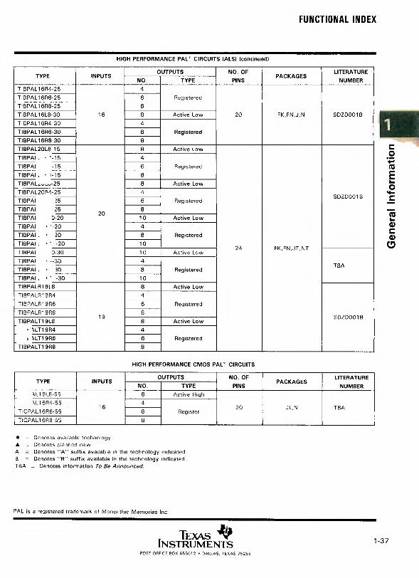
HIGH PERFORMANCE PAL' CIRCUITS (ALS)
TYPE INPUTS OUTPUTS NO. OF
PINS PACKAGES
LITERATURE
NUMBER NO. TYPE
406L8-10 8 Active High
4L16R4-10 4
TIBPAL16R6-10 6 Register
TIBPAL16R8-10 8 SDZDOO1B
TIBPAL16L8-12 8 Active High
TIBPAL16R4-12 4
TIBPAL16R6-12 6 Register
TIBPAL16R8-12
TIBPAL161-18-15 Active High TBA
TIBPAL16HD8-15 16 8 20 FK,FN,J,N
TIBPAL16L8-15 SDZDOO1 B Active Low
TIBPAL, 1-15 TBA
TIBPAL1 1,•.4-15
TlADAL" • • 15 6 Registered SDZDOO1B
\ L' • • 15 8
• AL, •• 25 8 Active High TBA
TIBPAL16FID8-25
TIRPAL16L8 25 . )001C 8 Active Low
• 4L16LD8-25
• = Denotes available technology
• = Denotes planned new.
A = Denotes "A" suffix available in the technology indicated
B = Denotes "B" suffix available in the technology indicated
TBA = Denotes information To Be Announced
PAL is a registered trademark of Monolithic Memories Inc.
TEXAS INSTRUMENTS
POST OFFICE BOX 665012 • DALLAS, TEXAS 75265
FUNCTIONAL INDEX
HIGH PERFORMANCE PAL' CIRCUITS (ALS) (continued)
TYPE INPUTS OUTPUTS NO. OF
PINS PACKAGES
LITERATURE
NUMBER NO. TYPE
TIBPAL16R4-25 4
TIBPAL16R6-25 6 Registered
TIBPAL16R8-25 8
TIBPAL16L8-30 16 8 Active Low 20 FK,FN,J,N SDZDOO1B
TIBPAL16R4-30 4
TIBPAL16R6-30 6 Registered
TIBPAL16R8-30 8
TIBPAL20L8-15 8 Active Low
TIBPAI . • '-15 4
TIBPAI -15 6 Registered
TIBPAI. • I-15 8
TIBPAL,_...,_..-25 8 Active Low
TIBPAL20R4-25 4
TIBPAI (5 6 Registered SDZD00113
TIBPAI 25 8 20
TIBPAI 0-20 10 Active Low
TIBPAI • '-20 4
TIBPAI. • 20 8 Registered
TIBPAI . • ' -20 10 24
TIBPAI 0-30 10 Active Low FK,FN,JT,NT
TIBPAI • •-30 4
TIBPAI. • 30 8 Registered TBA
TIBPAI . • ' 1-30 10
TIBPALR19L8 8 Active Low
TIBPALR19R4 4
TIBPALR19R6 6 Registered
TIBPALR19R8 8 19 SDZDOO1B
TIBPALT19L8 8 Active Low
• 4LT19R4 _ 4
_ . 4LT19R6 6 Registered
TIBPALT19R8 8
HIGH PERFORMANCE CMOS PAL' CIRCUITS
TYPE INPUTS OUTPUTS NO. OF
PINS PACKAGES
LITERATURE
NUMBER NO. TYPE
1..161..8-55
16
8 Active High
20 JL,N TBA kL16R4-55
— 4
Register TICPAL16R6-55 6
TICPAL16R8-55 8
• = Denotes available technology.
♦ Denotes planned new
A Denotes "A" suffix available in the technology indicated.
B Denotes "B" suffix available in the technology indicated.
TBA . Denotes information To Be Announced.
PAL is a registered trademark of Monolithic Memories Inc
TEXAS 40 INSTRUMENTS
Ge
ner
al In
form
atio
n
1 -37
POST OFFICE PDX 655012 • DALLAS. TEXAS 75265

uog
etw
olu
i le
JO
UG
D
FUNCTIONAL INDEX
1-38
HIGH PERFORMANCE IMPACT PROGRAMMABLE ARRAY LOGIC
TYPE INPUTS OUTPUTS NO. OF
PINS PACKAGES
LITERATURE
NUMBER NO TYPE
TIBPAL22V10 _ 12 Inputs or
11 Inputs
with CLK
10 I/O 24 NT,FN SDPS015
_ 4L22V10A
' 41_22V10A SDPS106
FIELD PROGRAMMABLE LOGIC ARRAY (ALS)
TYPE INPUTS OUTPUTS NO. OF
PINS ARRAY PACKAGES
LITERATURE
NUMBER NO. TYPE
TIFPLA839
14 6
3-State
24
14x32x6
FK,FN,N,NT
SDZ0001A
TIFPLA840 OC
TIB828167B 3-State
14 x 48 x 6 67A
2S105B 16 8
3-State 28 FK,FN,JD,N
. ' 05A 3-State
BIPOLAR MEMORY
FIRST-IN FIRST-OUT MEMORIES (FIFOs)
DESCRIPTION
TYPE
OF TYPE
TECHNOLOGY
PACKAGES LITERATURE
NUMBER STD
TTL ALS AS LS S HC HCT
16 Words x 4 Bits
3-State .. • J,N
SDVD001
3-State ..' •
3-State :-: A D,N,FK,FN
OC . • JN
OC . •
16 Words x 5 Bits
3-State . • J,N
3-State '229 A DW,FK,FN
3-State '234 • DW,J,FK,FN SDAS106
3-State A DW,FK,FN,J,N SDVD001
64 Words x 4 Bits 3-State . • DW,J,FK,FN SDAS107
64 Words x 5 Bits 3-State '235 • DW,FN,FK,N SDAS108
• Denotes available technology.
• Denotes planned new.
A Denotes "A" suffix available in the technology indicated
B Denotes "B" suffix available in the technology indicated.
TBA Denotes information To Be Announced.
Tr xias ANSI 1 ,Z1 'MENTS
POST OFFICE BOX 655012 • DALLAS, TEXAS 75265

Gen
era
l In
form
ati
on
GLOSSARY SYMBOLS, TERMS, AND DEFINITIONS
INTRODUCTION
These symbols, terms, and definitions are in accordance with those currently agreed upon by the JEDEC
Council of the Electronic Industries Association (EIA) for use in the USA and by the International Electrotechnical Commission (IEC) for international use.
OPERATING CONDITIONS AND CHARACTERISTICS (IN SEQUENCE BY LETTER SYMBOLS)
f max
Maximum clock frequency
The highest rate at which the clock input of a bistable circuit can be driven through its required
sequence while maintaining stable transitions of logic level at the output with input conditions
established that should cause changes of output logic level in accordance with the specification.
ICC Supply current
The current into the VCC supply terminal of an integrated circuit.
ICCH Supply current, outputs high The current into* the VCC supply terminal of an integrated circuit when all (or a specified number)
of the outputs are at the high level.
ICCL Supply current, outputs low
The current into* the VCC supply terminal of an integrated circuit when all (or a specified number)
of the outputs are at the low level.
IIH High-level input current The current into an input when a high-level voltage is applied to that input.
IIL Low-level input current
The current into* an input when a low-level voltage is applied to that input.
10H High-level output current The current into an output with input conditions applied that, according to the product
specification, will establish a high level at the output.
IOL Low-level output current The current into* an output with input conditions applied that, according to the product specification, will establish a low level at the output.
IOS Short-circuit output current The current into* an output when that output is short-circuited to ground (or other specified
potential) with input conditions applied to establish the output logic level farthest from ground potential lor other specified potential).
10Z Off-state (high-impedance-state) output current (of a three-state output) The current flowing into an output having three-state capability with input conditions established that, according to the production specification, will establish the high-impedance state at the output.
to Access time
The time interval between the application of a specified input pulse and the availability of valid signals at an output.
'Current out of a terminal is given as a negative value
TEXAS INSTRUMENTS 1-39
POST OFFICE BOX 655012 • DALLAS, TEXAS 75265

UO
UE
WJ
OJ
UI le
JOU
OD
GLOSSARY SYMBOLS, TERMS, AND DEFINITIONS
1-40
tdis Disable time (of a three-state output)
The time interval between the specified reference points on the input and output voltage waveforms, with the three-state output changing from either of the defined active levels (high or low) to a
high-impedance (off) state. (tdis = tPHZ or tPLZ)•
ten
Enable time (of a three-state output)
The time interval between the specified reference points on the input and output voltage waveforms,
with the three-state output changing from a high-impedance (off) state to either of the defined
active levels (high or low). (ten = tpZH or tpzLI.
tf Fall time The time interval between two reference points (90% and 10% unless otherwise specified) on
a waveform that is changing from the defined high level to the defined low level.
th Hold time
The time interval during which a signal is retained at a specified input terminal after an active
transition occurs at another specified input terminal.
NOTES: 1. The hold time is the actual time interval between two signal events and is determined by the system in which the digital circuit operates. A minimum value is specified that
is the shortest interval for which correct operation of the digital circuit is guaranteed.
2. The hold time may have a negative value in which case the minimum limit defines the longest interval (between the release of the signal and the active transition) for
which correct operation of the digital circuit is guaranteed.
tpd Propagation delay time The time between the specified reference points on the input and output voltage waveforms with
the output changing from one defined level (high or low) to the other defined level. (tpd = tPHL
or tPLH)•
tPHL
Propagation delay time, high-to-low level output
The time between the specified reference points on the input and output voltage waveforms with
the output changing from the defined high level to the defined low level.
tpHZ
Disable time (of a three-state output) from high level The time interval between the specified reference points on the input and the output voltage
waveforms with the three-state output changing from the defined high level to a high-impedance
(off) state.
tPLH
Propagation delay time, low-to-high-level output The time between the specified reference points on the input and output voltage waveforms with the output changing from the defined low level to the defined high level.
tpLZ
Disable time (of a three-state output) from low level
The time interval between the specified reference points on the input and output voltage waveforms with the three-state output changing from the defined low level to a high-impedance (off) state.
tpZH
Enable time (of a three-state output) to high level The time interval between the specified reference points on the input and output voltage waveforms with the three-state output changing from a high-impedance (off) state to the defined high level.
tpzL
Enable time (of a three-state output) to low level The time interval between the specified reference points on the input and output voltage waveforms
with the three-state output changing from a high-impedance (off) state to the defined low level.
TEXAS 4 INSTRUMENTS
POST OFFICE BOX 655012 • DALLAS. TEXAS 75265

■ C O
R
O
C
O
a)
GLOSSARY SYMBOLS, TERMS, AND DEFINITIONS
tr Rise time The time interval between two reference points (10% and 90% unless otherwise specified) on a waveform that is changing from the defined low level to the defined high level.
tsu Setup time The time interval between the application of a signal at a specified input terminal and a subsequent active transition at another specified input terminal.
NOTES: 1. The setup time is the actual time interval between two signal events and is determined
by the system in which the digital circuit operates. A minimum value is specified that
is the shortest interval for which correct operation of the digital circuit is guaranteed.
2. The setup time may have a negative value in which case the minimum limit defines
the longest interval (between the active transition and the application of the other signal) for which correct operation of the digital circuit is guaranteed.
tt
Transition time (general) The time interval between two reference points (10% and 90% unless otherwise specified) on a waveform that is changing from the defined low level to the defined high level (rise time) or from
the defined high level to the defined low level (fall time).
tw Pulse duration (width)
The time interval between specified reference points on the leading and trailing edges of the pulse
waveform.
VIH High-level input voltage An input voltage within the more positive (less negative) of the two ranges of values used to
represent the binary variables. NOTE: A minimum is specified that is the least-positive value of high-level input voltage for which
operation of the logic element within specification limits is guaranteed.
V11 Low-level input voltage An input voltage level within the less positive (more negative) of the two ranges of values used
to represent the binary variables. NOTE: A maximum is specified that is the most-positive value of low-level input voltage for which
operation of the logic element within specification limits is guaranteed.
VOH High-level output voltage The voltage at an output terminal with input conditions applied that, according to the product specification, will establish a high level at the output.
VOL Low-level output voltage The voltage at an output terminal with input conditions applied that, according to the product
specification, will establish a low level at the output.
VT+ Positive-going threshold level The voltage level at a transition-operated input that causes operation of the logic element according
to specification as the input voltage rises from a level below the negative-going threshold voltage,
VT — .
VT— Negative-going threshold level The voltage level at a transition-operated input that causes operation of the logic element according to specification as the input voltage falls from a level above the positive-going threshold voltage,
VT + •
TEXAS INSTRUMENTS
1-41
POST OFFICE BOX 655012 • DALLAS. TEXAS 75265

1
UO
IIM
UJO
IU1
lele
tlaD

Gen
eral In
form
atio
n
EXPLANATION OF FUNCTION TABLES
The following symbols are used in function tables on TI data sheets:
high level (steady state)
L = low level (steady state)
= transition from low to high level
= transition from high to low level
value/level or resulting value/level is routed to indicated destination
value/level is re-entered
X = irrelevant (any input, including transitions)
off (high-impedance) state of a 3-state-output
a .. h = the level of steady-state inputs at inputs A through H respectively
00 = level of Q before the indicated steady-state input conditions were established
Q0 complement of Qo or level of Q before the indicated steady-state input conditions were established
Qn level of Q before the most recent active transition indicated by 1 or t
J—L one high-level pulse
one low-level pulse
TOGGLE each output changes to the complement of its previous level on each active transition
indicated by 1 or t
If, in the input columns, a row contains only the symbols H, L, and/or X, this means the indicated output is valid whenever the input configuration is achieved and regardless of the sequence in which it is achieved.
The output persists so long as the input configuration is maintained.
If, in the input columns, a row contains H, L, and/or X together with t and/or 1, this means the output
is valid whenever the input configuration is achieved but the transition(s) must occur following the
achievement of the steady-state levels. If the output is shown as a level (H, L, Q0, or Q0), it persists
so long as the steady-state input levels and the levels that terminate indicated transitions are maintained.
Unless otherwise indicated, input transitions in the opposite direction to those shown have no effect at the output. (If the output is shown as a pulse, JL o r , the pulse follows the indicated input transition and persists for an interval dependent on the circuit.)
TEXAS INSTRUMENTS 1-43
POST OFFICE BOX 655012 • DALLAS, TEXAS 75265

uop
m.w
olui
ieJ
oueD
EXPLANATION OF FUNCTION TABLES
1-44
Among the most complex function tables in this book are those of the shift registers. These embody most
of the symbols used in any of the function tables, plus more. Below is the function table of a 4-bit
bidirectional universal shift register, g., type SN74194.
FUNCTION TABLE
INPUTS OUTPUTS
CLEAR MODE
Si SO CLOCK
SERIAL
LEFT RIGHT A
PARALLEL
B C D OA OB OC OD
==
==
=2
2
X X
=
2I
-,-
,-
■
X X
=
-,-1
22
-,
X-
, x
X X
X
=
-■
X X
X
X X
X
X
X
I
--J X
X X
-o
X X
X
X >
d
X X
.X
X
X
X
X
X X
=X
X X
X X
X X
m X
X X
X X
L
0A0 a
H
L
08n
°Br)
0A0
L
OBO b
DA,
ClA n
°Cn
0Cn
°B0
L
°CO c
°Bn
0 55
°Dn
ODn
°CO
L
°DO d
°Cn
°On
H
L
°DO
The first line of the table represents a synchronous clearing of the register and says that if clear is low, all
four outputs will be reset low regardless of the other inputs. In the following lines, clear is inactive (high)
and so has no effect.
The second line shows that so long as the clock input remains low (while clear is high), no other input has
any effect and the outputs maintain the levels they assumed before the steady-state combination of clear high and clock low was established. Since on other lines of the table only the rising transition of the clock
is shown to be active, the second line implicitly shows that no further change in the outputs will occur while
the clock remains high or on the high-to-low transition of the clock.
The third line of the table represents synchronous parallel loading of the register and says that if S1 and SO
are both high then, without regard to the serial input, the data entered at A will be at output QA, data entered
at B will be at GB, and so forth, following a low-to-high clock transition.
The fourth and fifth lines represent the loading of high- and low-level data, respectively, from the shift-right
serial input and the shifting of previously entered data one bit; data previously at QA is now at QB, the previous
levels of QB and Qc are now at Qc and QD respectively, and the data previously at QD is no longer in the
register. The entry of serial data and shift takes place on the low-to-high transition of the clock when S
is low and SO is high and the levels at inputs A through D have no effect.
The sixth and seventh lines represent the loading of high- and low-level data, respectively, from the shift-left
serial input and the shifting of previously entered data one bit; data previously at QB is now at QA, the previous levels of Qc and QD are now at QB and Qc, respectively, and the data previously at CIA is no longer in the
register. This entry of serial data and shift takes place on the low-to-high transition of the clock when S1
is high and SO is low and the levels at inputs A through D have no effect.
The last line shows that as long as both mode inputs are low, no other input has any effect and, as in the
second line, the outputs maintain the levels they assumed before the steady-state combination of clear high
and both mode inputs low was established.
TrxAs 1Ns1 RI 1MENTS
POST OFFICE BOX 655012 • DALLAS TEXAS 75265

Gen
eral In
form
ati
on
REMAINING
INPUTS
OPEN
NOTE: Each input is tested separately.
FIGURE 3. Vi
FIGURE 2. VII• VIL. VOL
II or IIH 1+)_11.
VI
REMAINING 0_
INPUTS
(See Note El
Vcc
OUTPUT IS)
OPEN OUTPUT IS)
OPEN
PARAMETER MEASUREMENT INFORMATION
SERIES 54/74, 54LS/74LS, 54S/74S
INPUT
CONDITIONS
(See Test Table
and Note)
Vcc OPEN.
COLLECTOR
OUTPUTS 1 0H
4- 1+1 VOH
TOTEM-POLE
OUTPUTS
IOH "—
VOH —
41-
NOTE: For functions having three-state outputs, input conditions
are maintained which will cause the outputs to be enabled
(low-impedance).
Vcc
loL 4— 1+1
VOL
NOTE: For functions having three-state outputs, input conditions
are maintained which will cause the outputs to be enabled
(low-impedance).
TEST TABLE
FUNCTION INPUT CONDITIONS
NAND Input under test at VIL max, all others at 4.5 V
AND All inputs at VIH min
NOR All inputs at VIL max
OR Input under test at VIH min, all others at GND
AND-OR
INVERT
Inputs under test la set including one input of
each AND gate) at VIE max, all others at 4.5 V
AND-OR All inputs of AND gate under test
at VIH min, all others at GND
TEST TABLE
FUNCTION INPUT CONDITIONS
NAND All inputs at VIH min
AND Input under test at VIL max, all others at 4.5 V
NOR Input under test at VIH min, others at GND
OR All inputs at VIL max
AND-OR-
INVERT
All inputs of AND gate under test
at VIH min, all others at GND
AND-OR Inputs under test la set including one input of
each AND gate) at VIH min, all others at 4.5 V
INPUT
CONDITIONS
(See Test Table
and Note)
FIGURE 1. VIH , VIL, VOH , 1 0H
vcc
_L NOTES: A. Each input is tested separately.
B. When testing AND-OR-INVERT or AND-OR gates,
each AND gate is tested separately with inputs of AND
gates not under test open when testing II and grounded when testing IIH
FIGURE 4. II, IIH
TEXAS 1 - 45 INSTRUMENTS
POST OFFICE BOX 655012 • DALLAS, TEXAS 75265

REMAINING
INPUTS
1 IL 4— -
VI
VCC
INPUT
(See Test Table
and Note) —
CONDITIONS
vt I
4, los
FUNCTION INPUT CONDITIONS FOR lecH INPUT CONDITIONS FOR lcu
NAND All inputs at GND All inputs at 4.5 V
AND All inputs at 4.5 V All inputs at GND
NOR All inputs at GND One input at 4.5 V,
all others at GND
OR One input at 4.5 V
all others at GND All inputs at GND
AND-OR-INVERT All inputs at GND All inputs of one AND gate
at 4.5 V, all others at GND
AND-OR All inputs of one AND gate
at 4 5 V, all others at GND All inputs at GND
(+1
'CC
VCC
INPUT r
CONDITIONS
(See Test Table
and Note) —
OUTPUTIS)
OPEN
PARAMETER MEASUREMENT INFORMATION
SERIES 54/74, 54LS/74LS, 54S/74S
4.5 V VCC
uog
ew
aolu
i le
ieueo
OUTPUT(S)
OPEN
NOTES. A. Each Input is tested separately.
B. When testing AND-OR-INVERT or AND-OR gates, each AND
gate is tested separately with input of AND gates not under test
open
FIGURE 5. III
FIGURE 6. 10S. 1 0
TEST TABLE
FUNCTION INPUT CONDITIONS
NAND All inputs at GND
AND All inputs at 4.5 V
NOR All inputs at GND
OR All inputs at 4.5 V_
AND-OR-INVERT All inputs at '. _
AND-OR All inputs at 4., .
NOTE: For functions having three-state
outputs, input conditions are main-
tained which will cause the outputs
to be enabled llowdrnpedancel.
TEST TABLE
NOTE: Icc is measured simultaneously for all functions in a package. The average-per-gate values are calculated
from the appropriate one of the following equations.:
total Icc. IccH, or Ica_ lcc, IcCH, or Icct, (average per gate or flip-flop) -
(number of gates or flip-flops in package)
ICCH T ICCL
2 (number of gates in package)
FIGURE 7. Icc
1-46
INSTRUMENTS TEXAS ,to
!cc (average per gate, 50% duty cycle) -
POST OFFICE BOX 655012 • DALLAS. TEXAS 75265

Ge
nera
l In
form
ati
on
VBE (0)
1 0L 4— 1-0
=27 kit
(Adjust lx)
PARAMETER MEASUREMENT INFORMATION
SERIES 54/74, 54LS/74LS, 54S/74S
VT
FIGURE 8. V-r+, IT + , VOL
(FOR NAND SCHMITT TRIGGERS)
VCC
IOL OPEN
4-1+1 0 2
FIGURE 9. VT – , IT VON (FOR NAND SCHMITT TRIGGERS)
NOTES: A. Switches are in position 1 for SN54'/SN74'
B. The IX limit for SN54' and SN74' circuits may be
verified by an alternate equivalent procedure. The
Vgx source is replaced by a resistor (see table
below) in parallel with a voltmeter between the X
and X pins. If the measured voltage, Vxx, is less
than 0.4, the specified limit for ly( is met.
RESISTANCE VALUE TABLE
SN5423 114
SN5450, SN5453 138 0
SN7423 105 2 v)7
SN7450, SN7453 130 0
FIGURE 10. Ix (FOR EXPANDABLE GATES)
1-47
FIGURE 11. VBE(Q) (FOR EXPANDABLE GATES) FIGURE 12. VOH (FOR EXPANDABLE GATES)
Tr XAS INS1 RUM ENTS
POST OFFICE BOX 655012 • DALLAS, TEXAS 75265

PARAMETER MEASUREMENT INFORMATION
SERIES 54/74, 54LS/74LS, 54S/74S
uo!
leu
uo
lui le
ieu
eD
4— (--) x
FIGURE 13. VOH (FOR EXPANDABLE GATES)
IX 4--1+1
V111
4— (-1 IX
FIGURE 14. Vol_ (FOR EXPANDABLE GATES)
IX
4.5 V
VCC
(+) V5Z
x
V IL
VCC
FIGURE 15. ON-STATE CHARACTERISTICS FIGURE 16. OFF-STATE CHARACTERISTICS FOR EXPANDERS
vcc
FOR EXPANDERS
VCC
4.5 V
4— (+1 Ix
4-- (+1 IX
vx
VIL
FIGURE 17. ON-STATE CHARACTERISTICS FIGURE 18. OFF-STATE CHARACTERISTICS
VIH
FOR EXPANDERS FOR EXPANDERS
I Vcc
(See Notes
2 and 3) —
OTHER
INPUTS
1 01offl
4— 1+1 (See Note 2)
(See Note 3)
To Vg..1 Of VIL
(See Note 11 —
OUTPUT
CONTROL
INPUTS
NOTES: 1. Input conditions are maintained which will ensure that the three-state outputis) is (are) disabled to the high-impedance state. See function table or logic for the particular device.
Vo 2. When testing for current into the output with a high-level output voltage, input conditions are applied that would cause the output to be low if it were enabled.
3. When testing for current out of the output with a low-level output voltage, input conditions are applied that would cause the output to be high if it were enabled.
FIGURE 19. lo( off) (THREE-STATE OUTPUTS)
TEXAS 4 INSTRUMENTS
1 -48
POST OFFICE BOX 655012 • DALLAS. TEXAS 75265

FROM OUTPUT
UNDER TEST
(See Note B)
CL (See Note A/ ..1 .•
TEST
POINT
CL
T (See Note A)
FROM OUTPUT
UNDER TEST
PARAMETER MEASUREMENT INFORMATION
SERIES 54/74 and 54S/74S
TEST
POINT TEST
POINT VCC VCC
VCC
Gen
era
l In
form
ati
on
FROM OUTPUT
UNDER TEST
CL (See Note A)
S1
(See Note B)
S2
LOAD CIRCUIT FOR
HI-STATE
LOAD CIRCUIT FOR LOAD CIRCUIT FOR
TOTEM-POLE OUTPUTS
OPEN-COLLECTOR OUTPUTS THREE-STATE OUTPUTS
NOTES: A. CL includes probe and jig capacitance.
B. All diodes are 1N3064 or equivalent
NPUTG
1.5 V
3 V HIGH-LEVEL /
1.5 V 1.5 V 4 I
l.
0V PULSE
TIMIN
4...._tw ____04
,,r, iii thold tsatup 4 41--two 4 3 V
DATA j 1.5 V INPUT
\1.5 V LOW-LEVEL Thi\
i 1.5 V 1.5 V
0 V PULSE
VOLTAGE WAVEFORMS VOLTAGE WAVEFORMS
SETUP AND HOLD TIMES PULSE WIDTHS
3 V OUTPUT 3 V
INPUT 1.5 V 1.5 V CONTROL j I
\ \ 1.5 V 1.5 V
I 111--lertPHL enabling/
(Low-level 0 V
,
I 0 V
I4— , PZL-11.1 (4 tPLZ
IN-PHASE
PLH-14—II1 I I
OUTPUT I
1 I \__.-t- , 5 v -4.5 V I S2 closed 1 WAVEFORM 1 St closed,
NI,.
1.5 V
I alK - 4
I S1 and
1.5 V -1.5 V
VOH
tpHL46-11.1 I VOL (See Note Cl S2 open
I4-4*-tPLH i 10.5 V VOL
OUT-OF-PHASE
OUTPUT I 1.5V i i 17V "H
eli---tPZH—Ill tPHZ-14-101 EO.5 V
I
I
H
VOL WAVEFORM 2 Si open, N--f
(See Note CI S2 closed / 1 5 V -
V1
O.5 V
0 V S1 and
S2 closed
VOLTAGE WAVEFORMS VOLTAGE WAVEFORMS
PROPAGATION DELAY TIMES ENABLE AND DISABLE TIMES, THREE-STATE OUTPUTS
NOTES: C. Waveform 1 is for an output with internal conditions such that the output is low except when disabled by the output control.
Waveform 2 is for an output with internal conditions such that the output is high except when disabled by the output control. D. In the examples above, the phase relationships between inputs and outputs have been chosen arbitrarily.
E. All input pulses are supplied by generators having the following characteristics: PRR < 1 MHz, Z out = 50 0 and:
For Series 54/74, t r W. 7 ns, tf 7 ns.
For Series 54S/74S, t r s 2.5 ns, If 2.5 ns.
F. When measuring propagation delay times of 3-state outputs, switches S1 and S2 are closed. G. The outputs are measured one at a time with one input transition per measurement.
TEXAS INSTRUMENTS
POST OFFICE BOX 655012 • DALLAS. TEXAS 75265
(See Note F)
4 1 -49

FROM OUTPUT UNDER TEST
CL
(See Note Al
LOAD CIRCUIT FOR
BI-STATE
TOTEM-POLE OUTPUTS
NOTES A CL includes probe and Jig capacitance
B. All diodes are 1 N3064 or equivalent.
FROM OUTPUT UNDER TEST TEST
POINT
cL
i ISee Note Al
=
-=t
LOAD CIRCUIT FOR
LOAD CIRCUIT FOR
OPEN-COLLECTOR OUTPUTS THREE-STATE OUTPUTS
uog
ew
iNui
IR
JOU
O9
FROM OUTPUT UNDER TEST
CL
(See Note Al
S
PARAMETER MEASUREMENT INFORMATION
SERIES 54LS/74LS
TEST
POINT
VCC TEST
POINT VCC
VCC
- 0 V
3 V
INPUT TIMING
411.3 V
0 V PULSE HIGH-LEVEL
/1.3 V 1.3 V i aiii II ',hold 14---1w--114
tsetup 14 4--1w --lel -1. 3 V T'
.3 V DATA j1.3 V
LOW-L ---\1.3 V \1.3V 1 INPUT PULSE
0 V
VOLTAGE WAVEFORMS VOLTAGE WAVEFORMS
SETUP AND HOLD TIMES PULSE WIDTHS
3 V OUTPUT 3 V
INPUT _11.3 V I
\1.3 V CONTROL V 1 3 V
I 0 V (Low-level
14-41-tPHL enabling) 14—tPZL-11.1 14-14- tPLZ
1 tPLH /4-01
IN-PHASE OUTPUT I I
VOH I I I
1.3 V 1 \__, t 1.3"
WAVEFORM 1
1
1.3 V I
-4.5 V I I Si and
S2 closed
I 1 VOL (See Note Cl S2 open Si closed, ‘
I i - 4 1.5 V
tpHL--14---101 14-114- 1PLH i 10.5 V
VOL
OUT-OF-PHASE OUTPUT
-----\ 1.3 V
I VOH 4— , PZH — 1.3 V
101 I
VH2-14—►4
1
VOL
i0.5 V
(See Note Fl WAVEFORM 2 51 open, I 1.3 V `
__f -.1.5 VOH
ISee (See Note Cl S2 dosed S1 and S2 closed
VOLTAGE WAVEFORMS VOLTAGE WAVEFORMS
PROPAGATION DELAY TIMES ENABLE AND DISABLE TIMES, THREE-STATE OUTPUTS
NOTES: C. Waveform 1 is for an output with internal conditions such that the output is low except when disabled by the output control
Waveform 2 is for an output with internal conditions such that the output is high except when disabled by the output control.
D. In the examples above, the phase relationships between inputs and outputs have been chosen arbitrarily.
E. All input pulses are supplied by generators having the following characteristics: PRR < 1 MHz, Z ou t = 50 0 and for Series
54LS/74LS, t r s 1.5 ns, tr s 2.6 ns.
F. When measuring propagation delay times of 3-state outputs, switches S1 and S2 are closed.
G. The outputs are measured one at a time with one input transition per measurement.
1-50 TEXAS INSTRUMENTS
POST OFFICE BOX 655012 • DALLAS, 11XAS 75205

4.0
3.6 Mil. 30 TA = -55 E
2.5
Ni , 2.0
li. :;'
TA - 25'C
0 1.5 i
O
1.0 ! 1 1A = 125'E-
h 1 I i 0 5
0 I 02 04 06 00 1 12 14 16 16 2
V1--Input Voltage-V
VCS 5V
RL • 400 S-1
TA • -55°C
0 5
0 1_ I 0 -5 -10 -15 -20 -25 -30
10H-High-Level Output Current-mit
06
0.5
I !
- I I VEE = 5 V VI • 2.4 V TA. -55°C
40
► 35
30 1111111IMN MOW! • t OA
O
•
0.3 25
,t 20
02 - CL =
0 EL = 15 pF I
IN '
0 I L _1 - 75 -50 -25 0 5 50 75 100 125
TA -Free Air T roperature-"C
25 15 10 20 35 40 30
IOL - Low Level-Output Currant-OA
40
FVEC 5 1., 1;11
35 - RI. 40011 • •
E 1—
E.; 0 25
20
15
it to
30
s 25 co
II 20 14 15
21
FIGURE A3
PROPAGATION DELAY TIME, LOW-TO-HIGH LEVEL OUTPUT
vs rerr AIR TEMPERATURE.
meincL.,54F mos
-75 -50 -25 0 25 50 75 100 125
TA-Free Alf Tempe ature-° C
FIGURE A5
FIGURE A4
PROPAGATION DELAY TIME. HIGH-T0•1-0141.LEVEL OUTPUT
vs
FREE AIR TEMPERATURE
40 -
VEc - 5 V 26 r RL=400 11
- 75 -50 -25 0 25 50 75 100 125
7 A Free AirT mper tore- ° C
FIGURE A6
TYPICAL CHARACTERISTICS
SERIES 54/74t
OUTPUT VOLTAGE
INPUT VOLTAGE
FIGURE Al
LOW.LEVEL OUTPUT VOLTAGE vs
LOW LEVEL OUTPUT CURRENT
111511 LEVEL OUTPUT VOLTAGE
HIGH-LEVEL OUTPUT CURRENT
FIGURE A2
AVERAGE PROPAGATION DELAY TIME vs
FREE AIR TEMPERATURE
tData for temperatures below 0°C and above 70°C are applicable for Series 54 circuits only. Data as shown are applicable specifically for the NAND gates with totem-pole outputs.
4 TEXAS INSTRUMENTS
1-51
POST OFFICE BOX 055012 • DALLAS. TEXAS 75255

CD
CD
uog
ewA
olu
i
LOW-LEVEL OUTPUT VOLTAGE vs
LOW-LEVEL OUTPUT CURRENT (STANDARD OUTPUT)
VCc vi
- 5 V 2 V
TA = 125°C
TA = -55°C/ TA = 25°C
1 2 3 4 5 6 7 B 9 10
10L — Low Le el Outpu Current—mA
FIGURE D3
POWER DISSIPATION PER GATE
FREQUENCY
OUTPUT VOLTAGE
vs INPUT VOLTAGE
IPNP INPUT)
4.0
3.5
.o
25
2.0
5
5 I 0
0.5
ik 0.4
3
O
01 O
0 02 0.4 0 6 0 8 1 12
1.6 18 2
put Volt, ge—V
FIGURE D2
LOW-LEVEL OUTPUT VOLTAGE vs
LOW-LEVEL OUTPUT CURRENT (BUFFER OUTPUT)
INL—Low Level 0 tout Current ;r1A
VO
L—
Lo
w-L
ev
el O
utp
ut
Vo
ltag
e—
V
FIGURE D4
HIGH-LEVEL OUTPUT VOLTAGE
vs HIGH-LEVEL OUTPUT CURRENT
00 -10 -20 -30 -40 -50 -60 -70
10,-1-11411 Level Output Current -mil
FIGURE D5
-80
4.0
3.5
I4 3.0
5 2.5
tf, 2.0
7-;
E.' OS
VCC =5V
TA = 25° C
TA = 25 ° C
PO
—P
ow
er
Dis
sip
atio
n P
er G
ate—
mW
2 VCC= 5 v
TA = 25° C Duty Cycle
1111111
15
CL - 2
al_ .21 1- .I 10—
0.1 0.4 1 4 40
I--Frequency—MHz
FIGURE D6
20
113
1.; 14
4
2
0 10 20 30 40 50 60 70 80 90 100
CL-Load Capecitance-pF
FIGURE D8
-75 -50 -25 0 25 50 75 100 125
TA-Free-Air Temperature- ° C
FIGURE D7
tData for temperatures below 0°C and above 70°C are applicable for Series 54LS circuits only.
TEXAS INSTRUMENTS
1-52 4,4#
TYPICAL CHARACTERISTICS
SERIES 54LS/74LSt
OUTPUT VOLTAGE
vs
INPUT VOLTAGE
(DIODE INPUT) elms vcc -sv RL = 2 kfit
MEMO!
_
n
TA - 25 ° C
TA=125 C
TA -- - 55C
0 0.2 04 06 08 1 12 1 4 1 6 1 8 2
v i --i Tut Volt 91—V
FIGURE D1
2.0
U 15
5 10
OS
PROPAGAT 10,1 DLEAY 1 5 1 1 1101 1 AerATION DELAY TIMES
vs
F FILE AIR TEMPERATURE
LOAD CAPACITANCE
POST OFFICE BOX 655012 • DALLAS, TEXAS 75265

40
3.0
.82 2.5
20
1.5
1.0
0
0,JFITcrT
116010 VO4766,1'
:0 TT-rsst7
12
SERIES 54S/74St
0.92
I 0.88
—0.84
-0.80 a t —0.76
0.72
, 0 68
— 064
0.60
Vcc = !Li EL = 280 EINIERIL
OM ■■■■■11111 ■■
MINIM
1
Ge
ne
ral In
form
ati
on
0 02 04 0.6 08 10 1.2 1.4 16 1 8 2 0
V1—Input Voltage—V
FIGURE El
—75 —50 —25 0 25 50 76 100 126
TA—Free-Air Tempe eture— °C
FIGURE E2
FIGURE E3
INPUT CURRENT
INPUT VOLTAGE
FIGURE E4
HIGH LEVEL INPUT CURRENT
FREE-AIR TEMPERATURE 10
4
.11 2
VCC = 5. Vi • 2.7 1.
07
.06 94
02
o 1 .5. 0 07
004
0 02
0.01 —75 —50 —26 0 25 60 75 100 125
Iq sErcesAir Temperature—C
LOW-LEVEL OUTPUT VOLTAGE vs
LOW-LEVEL OUTPUT CURRENT
I0L—Low-Level Output Current—mA
HIGH-LEVEL OUTPUT VOLTAGE
HIGH-LEVEL OUTPUT CURRENT
I TA -
0 —10 —20 —30 —40 —50 —60 —70 —80
JOH—HO-Level Output Current—mA
INPUT CLAMPING DIODE
FORV:ARD VOLTAGE
vs
1 - 1iLl - AIR TEMPERATURE
L„,_ 5 V
■■■■■■■■ ■NEIN■■■■■ ENRIFI ■20L —25 mA ■ "'AMINE.
I L°-10 rnA
TYPICAL CHARACTERISTICS
FIGURE E5
FIGURE E6
tData for temperatures below 0°C and above 70°C are applicable for Series 54S circuits only.
Data as shown are applicable specifically for the NAND gates with totem-pole outputs.
k; INSTRUMENTS
TEXAS 1-53
POST OFFICE BOX 665012 • DALLAS, TEXAS 75265

0 4.5 475 50 5.25
Vcc—Supply Voltage—V
7
10
$.7 9 S
5
a.
8' 4
a
PROPAGATION DELAY TIME, HIGH-TO-LOW-LEVEL OUTPUT
vs SUPPLY VOLTAGE
55 475 50 5.25
Vcc—Supply Voltage—V
RL 280 S2 TA 25°C -
CL . 150 pF
CL . 50 pF
CL 16 pF
1
0 45
10
9
4! rg 00 6
Kpp I 5
0; 4
51 3
FIGURE E8
55
CL . 150 pF
CL= 50 pF
15 pF
10 RL`28O0
TA 25°C -
FIGURE El 0
UO
IMU
IJO
IU1
IR
JOU
GD
• ■
125 —75 —50 —25 0 25 50 75 100
TA—Free.0,0 Temperature— ° C
EMM■N MINEIMIE
CL -15O pF..,
1.11110193111.! .11111MMEM11111111 MINCISIMENIESE
VCC 5 V RL 280 SI
Si
1 3 5 4
.7 i 3
M 2
10
if
28 6
FIGURE E7
PROPAGATION DELAY TIME,
HIGH-TO-LOW-LEVEL OUTPUT vs
FREE-AIR TEMPERATURE
anNM
v. RL - .250 5 V
a
r
EN Ili,
1 --8.1mmiglEill
CL= 50 pF
Illffilmill
—50 —25 0 25 50 75 100 125
TA—Free-AIR TEMPERATURE—° C
FIGURE E9
10
9
4
3
E 2
0
-75
80
; 70
° 50
40 a
2 30
0
POWER DISSIPATION PER GATE
FREQUENCY
VCC . 6 V CL .15 pF TA 26°C Duty Cycle 50%
AVERAGE PROPAGATION DELAY TIME vs
FREE-AIR TEMPERATURE
VCC - 5 V AL 280a
CL 150 pF
2 4 7 10 20 40 70 100
1 — F equency—MHz
FIGURE E12
—50 —25 0 25 60 75 100 125
TA—Free Air T I0PeraI 0 re—°0
FIGURE El 1
TYPICAL CHARACTERISTICS
SERIES 545/74S t
PROPAGATION DELAY TIME, PROPAGATION DELAY TIME,
LOW-TO-HIGH-LEVEL OUTPUT
LOW-TO-HIGH-LEVEL OUTPUT
vs
vs
FREE-AIR TEMPERATURE
SUPPLY VOLTAGE
1-54
tData for temperatures below 0°C and above 70°C are applicable for Series 54S circuits only.
Data as shown are applicable specifically for the NAND gates with totem-pole outputs.
TEXAS INSTRUMENTS
4 POST OFFICE BOX 855012 • DALLAS, TEXAS 75265

0
-2
4
6
HIGH LEVEL INPUT CURRENT V5
FR EEAIR TEMPERATURE
Vcc • 1, 4 VI. 2.7
04
0 0 2
01 r 0 07
1 004
002
001 -75 -60 -25
10
0 25 50
75 100 125
10
0.8 07
5 06
05
D
03
JO02
Ge
ner
al I
nfo
rma
tion
1 5112, 1 5113, '5114 AVERAGE PROPAGATION DELAY TIME,
CLOCK TO OUTPUT vs
LOAD CAPACITANCE
MCC` 5 _EL-280 02
TA •
2
-75 50 25 0 25 50 75 100 125 25 50 76 100 125 160 175 200 0 0
2112. 'S113, '5114 AVERAGE PROPAGATION DELAY TIME,
CLOCK TO OUTPUT vs
FREE-AIR TEMPERATURE
U....
CL 1 0 pF
J....C L .50pF
V66 .5 V R1 28011
16
14
c' 12
10
6
4
2
TYPICAL CHARACTERISTICS FOR FLIP-FLOPS
SERIES 54S/74S t
8 2
4 i
O
HIGH LEVEL OUTPUT VOLTAGE
vs HIGH LEVEL OUTPUT CURRENT
0 -10 -20 -30 -40 -50 -60 -70 -80
I0H-High-Level Output Current -mA
FIGURE E13
S112, 1 5113 INPUT CURRENT
vs INPUT VOLTAGE
. iorr
4 —
/K INPUTS I -- -1
4 1 ,--
PRESET/CLEAR INPUTS
CLOCKINPUT -
I 1
1 VCC = 5 V TA - 25°C
0 1 2 3 4
VI-Input Voltage-V
FIGURE E15
LOW-LEVEL OUTPUT VOLTAGE
LOW LEVEL OUTPUT CURRENT
VCCSV
-TA= -55°C
TA 25 C
-...!
MIIII4W,.. ,"" %1- I,/
TA = 125°C
- --/ - , I
FIGURE E14
TA-Free4ur Temperature- ° C
FIGURE E16
0 0 5 10 15 20 25 30 35 40
IOL-Low.Level Output Currant-PIA
CL-Load Capaenance-PE
FIGURE E17
tData for temperatures below 0°C and above 70°C are applicable for Series 54S circuits only.
FIGURE E18
TEXAS INSTRUMENTS
4 1-55
POST OFFICE BOX 655012 • DALLAS, TEXAS 76265

1