TS5USBC400 Datasheet - TI.com · • 0-V to 16-V Overvoltage Protection (OVP) on Common Pins ......
29
USB VCC D1- D2+ D1+ OVP Logic Control GND VBUS DP_T DP_B DM_T DM_B GND USB Connector TS5USBC400 Copyright © 2017, Texas Instruments Incorporated UART USB D2- SEL1 SEL2 OE FLT Product Folder Order Now Technical Documents Tools & Software Support & Community An IMPORTANT NOTICE at the end of this data sheet addresses availability, warranty, changes, use in safety-critical applications, intellectual property matters and other important disclaimers. PRODUCTION DATA. TS5USBC400 SCDS374A – SEPTEMBER 2017 – REVISED SEPTEMBER 2017 TS5USBC400 Dual 2:1 USB 2.0 Mux/DeMux with 16-V Overvoltage Protection 1 1 Features 1• Supply Range 2.3 V to 5.5 V • Differential 2:1 or 1:2 Switch/Multiplexer • 0-V to 16-V Overvoltage Protection (OVP) on Common Pins • Powered Off Protection When V CC =0V • Low R ON of 9 Ω Maximum • BW of 1.1 GHz Typical • C ON of 4.5 pF Typical • Low Power Disable Mode • 1.8-V Compatible Logic Inputs • ESD Protection Exceeds JESD 22 – 2000-V Human Body Model (HBM) • TS5USBC400: Standard Temperature Range of 0°C to 70°C • TS5USBC400I: Industrial Temperature Range of -40°C to 85°C • Small DSBGA Package 2 Applications • Mobile • PC/Notebook • Tablet • Anywhere a USB Type-C™ or Micro-B Connector is Used 3 Description The TS5USBC400 is a bidirectional low-power dual port, high-speed, USB 2.0 analog switch with integrated protection for USB Type-C™ systems. The device is configured as a dual 2:1 or 1:2 switch and is optimized for handling the USB 2.0 D+/- lines in a USB Type-C™ systems. The TS5USBC400 protection on the I/O pins can tolerate up to 16V with automatic shutoff circuitry to protect system components behind the switch. The TS5USBC400 comes in a small 12 pin DSBGA package making it a perfect candidate for mobile and space constrained applications. Device Information (1) PART NUMBER PACKAGE BODY SIZE (NOM) TS5USBC400 TS5USBC400I DSBGA (12) 1.582 mm × 1.182 mm (1) For all available packages, see the orderable addendum at the end of the data sheet. Simplified Schematic
Transcript of TS5USBC400 Datasheet - TI.com · • 0-V to 16-V Overvoltage Protection (OVP) on Common Pins ......

USB
VCC
D1-
D2+
D1+OVP
LogicControl
GND
VB
US
DP
_TD
P_B
DM
_TD
M_B
GN
D
USBConnector
TS5USBC400
Copyright © 2017, Texas Instruments Incorporated
UARTUSB
D2-
SEL1
SEL2
OE
FLT
Product
Folder
Order
Now
Technical
Documents
Tools &
Software
Support &Community
An IMPORTANT NOTICE at the end of this data sheet addresses availability, warranty, changes, use in safety-critical applications,intellectual property matters and other important disclaimers. PRODUCTION DATA.
TS5USBC400SCDS374A –SEPTEMBER 2017–REVISED SEPTEMBER 2017
TS5USBC400 Dual 2:1 USB 2.0 Mux/DeMux with 16-V Overvoltage Protection
1
1 Features1• Supply Range 2.3 V to 5.5 V• Differential 2:1 or 1:2 Switch/Multiplexer• 0-V to 16-V Overvoltage Protection (OVP) on
Common Pins• Powered Off Protection When VCC = 0 V• Low RON of 9 Ω Maximum• BW of 1.1 GHz Typical• CON of 4.5 pF Typical• Low Power Disable Mode• 1.8-V Compatible Logic Inputs• ESD Protection Exceeds JESD 22
– 2000-V Human Body Model (HBM)• TS5USBC400: Standard Temperature Range of
0°C to 70°C• TS5USBC400I: Industrial Temperature Range of
-40°C to 85°C• Small DSBGA Package
2 Applications• Mobile• PC/Notebook• Tablet• Anywhere a USB Type-C™ or Micro-B Connector
is Used
3 DescriptionThe TS5USBC400 is a bidirectional low-power dualport, high-speed, USB 2.0 analog switch withintegrated protection for USB Type-C™ systems. Thedevice is configured as a dual 2:1 or 1:2 switch and isoptimized for handling the USB 2.0 D+/- lines in aUSB Type-C™ systems.
The TS5USBC400 protection on the I/O pins cantolerate up to 16V with automatic shutoff circuitry toprotect system components behind the switch.
The TS5USBC400 comes in a small 12 pin DSBGApackage making it a perfect candidate for mobile andspace constrained applications.
Device Information(1)
PART NUMBER PACKAGE BODY SIZE (NOM)TS5USBC400TS5USBC400I DSBGA (12) 1.582 mm × 1.182 mm
(1) For all available packages, see the orderable addendum atthe end of the data sheet.
Simplified Schematic

2
TS5USBC400SCDS374A –SEPTEMBER 2017–REVISED SEPTEMBER 2017 www.ti.com
Submit Documentation Feedback Copyright © 2017, Texas Instruments Incorporated
Table of Contents1 Features .................................................................. 12 Applications ........................................................... 13 Description ............................................................. 14 Revision History..................................................... 25 Pin Configuration and Functions ......................... 36 Specifications......................................................... 4
6.1 Absolute Maximum Ratings ...................................... 46.2 ESD Ratings.............................................................. 46.3 Recommended Operating Conditions....................... 46.4 Thermal Information .................................................. 56.5 Electrical Characteristics........................................... 56.6 Dynamic Characteristics ........................................... 76.7 Timing Requirements ................................................ 76.8 Typical Characteristics .............................................. 8
7 Parameter Measurement Information .................. 98 Detailed Description ............................................ 13
8.1 Overview ................................................................. 13
8.2 Functional Block Diagram ....................................... 138.3 Feature Description................................................. 148.4 Device Functional Modes........................................ 16
9 Application and Implementation ........................ 179.1 Application Information............................................ 179.2 Typical Application .................................................. 17
10 Power Supply Recommendations ..................... 1811 Layout................................................................... 19
11.1 Layout Guidelines ................................................. 1911.2 Layout Example .................................................... 20
12 Device and Documentation Support ................. 2112.1 Documentation Support ........................................ 2112.2 Community Resources.......................................... 2112.3 Trademarks ........................................................... 2112.4 Electrostatic Discharge Caution............................ 2112.5 Glossary ................................................................ 21
13 Mechanical, Packaging, and OrderableInformation ........................................................... 21
4 Revision HistoryNOTE: Page numbers for previous revisions may differ from page numbers in the current version.
Changes from Original (September 2017) to Revision A Page
• Added ICC Active supply current and Supply current during OVP condition to the Electrical Specification table .................. 4

SEL1 D+ D- FLT
VCC SEL2 GND OE
D1+ D1-D2+ D2-
A
B
C
1 2 3 4
3
TS5USBC400www.ti.com SCDS374A –SEPTEMBER 2017–REVISED SEPTEMBER 2017
Submit Documentation FeedbackCopyright © 2017, Texas Instruments Incorporated
5 Pin Configuration and Functions
YFP Package12-Pin DSBGA
Top View
Pin FunctionsPIN
I/O DESCRIPTIONNAME NO.SEL1 A1 I Switch select1 (Active high)
D+ A2 I/O Data switch input (Differential +)D– A3 I/O Data switch input (Differential –)FLT A4 O Fault indicator output pin (Active low) - open drainVCC B1 PWR Supply VoltageSEL2 B2 I Switch select2 (Active high)GND B3 GND GroundOE B4 I Output enable (Active low)D2+ C1 I/O Data switch output 2 (Differential +)D2– C2 I/O Data switch output 2 (Differential -)D1+ C3 I/O Data switch output 1 (Differential +)D1– C4 I/O Data switch output 1 (Differential -)

4
TS5USBC400SCDS374A –SEPTEMBER 2017–REVISED SEPTEMBER 2017 www.ti.com
Submit Documentation Feedback Copyright © 2017, Texas Instruments Incorporated
(1) Stresses beyond those listed under Absolute Maximum Ratings may cause permanent damage to the device. These are stress ratingsonly, which do not imply functional operation of the device at these or any other conditions beyond those indicated under RecommendedOperating Conditions. Exposure to absolute-maximum-rated conditions for extended periods may affect device reliability.
(2) The algebraic convention, whereby the most negative value is a minimum and the most positive value is a maximum.(3) All voltages are with respect to ground, unless otherwise specified.
6 Specifications
6.1 Absolute Maximum Ratingsover operating free-air temperature range (unless otherwise noted) (1) (2)
MIN MAX UNITVCC Supply voltage (3) –0.5 6 VVI/O Input/Output DC voltage (D+, D-) (3) –0.5 18 VVI/O Input/Output DC voltage (D1+/D1-, D2+/D2-) (3) –0.5 6 VVI Digital input voltage (SEL1, SEL2, OE) –0.5 6 VVO Digital output voltage (FLT) –0.5 6 V
IKInput-output port diode current (D+, D-,D1+, D1-, D2+, D2-) VIN < 0 –50 mA
IIKDigital logic input clamp current (SEL1,SEL2, OE) (3) VI < 0 –50 mA
ICC Continuous current through VCC 100 mAIGND Continuous current through GND –100 mATstg Storage temperature –65 150 °C
(1) JEDEC document JEP155 states that 500-V HBM allows safe manufacturing with a standard ESD control process.(2) JEDEC document JEP157 states that 250-V CDM allows safe manufacturing with a standard ESD control process.
6.2 ESD RatingsVALUE UNIT
V(ESD)Electrostaticdischarge
Human body model (HBM), per ANSI/ESDA/JEDEC JS-001 (1) ±2000V
Charged-device model (CDM), per JEDEC specification JESD22-C101 (2) ±1000
6.3 Recommended Operating ConditionsMIN MAX UNIT
VCC Supply voltage 2.3 5.5 VVI/O (D+, D-) Analog input/output voltage
0 18 VVI/O (D1, D1-, D2+, D2-) 0 3.6 VVI Digital input voltage (SEL1, SEL2, OE) 0 5.5 VVO Digital output voltage (FLT) 0 5.5 VII/O (D+, D-, D1+, D1-, D2+, D2-) Analog input/output port continuous current -50 50 mAIOL Digital output current 3 mATA Operating free-air temperature (TS5USBC400) Standard 0 70 ºCTA Operating free-air temperature (TS5USBC400I) Industrial –40 85 ºCTJ Junction temperature –40 125 ºC

5
TS5USBC400www.ti.com SCDS374A –SEPTEMBER 2017–REVISED SEPTEMBER 2017
Submit Documentation FeedbackCopyright © 2017, Texas Instruments Incorporated
(1) For more information about traditional and new thermal metrics, see the Semiconductor and IC Package Thermal Metrics applicationreport.
6.4 Thermal Information
THERMAL METRIC (1)TS5USBC400
UNITYFP12 PINS
RθJA Junction-to-ambient thermal resistance 91.8 °C/WRθJC(top) Junction-to-case (top) thermal resistance 0.8 °C/WRθJB Junction-to-board thermal resistance 22.8 °C/WψJT Junction-to-top characterization parameter 0.5 °C/WψJB Junction-to-board characterization parameter 23.0 °C/W
6.5 Electrical CharacteristicsTA = –40°C to +85°C (Industrial), TA = 0 to 70 (Standard), VCC = 2.3 V to 5.5 V, GND = 0V, Typical values are at VCC =3.3 V, TA = 25°C, (unless otherwise noted)
PARAMETER TEST CONDITIONS MIN TYP MAX UNITSUPPLYVCC Power supply voltage 2.3 5.5 V
ICC
Active supply currentOE = 0 VSEL1, SEL2 = 0 V, 1.8 V or VCC0 V < VI/O < 3.6 V
72 100 µA
Supply current during OVP conditionOE = 0 VSEL1, SEL2 = 0 V, 1.8 V or VCCVI/O > VPOS_THLD
80 120 µA
ICC_PDStandby powered down supplycurrent
OE = 1.8 V or VCCSEL1 = 0 V, 1.8 V, or VCCSEL2 = 0 V, 1.8 V, or VCC
2.2 10 µA
DC Characteristics
RON ON-state resistanceVI/O = 0.4 VISINK = 8 mARefer to ON-State Resistance Figure
5.6 9 Ω
ΔRONON-state resistance match betweenchannels
VI/O = 0.4 VISINK = 8 mARefer to ON-State Resistance Figure
0.07 0.3 Ω
RON (FLAT) ON-state resistance flatnessVI/O = 0 V to 0.4 VISINK = 8 mARefer to ON-State Resistance Figure
0.07 0.4 Ω
IOFF I/O pin OFF leakage current
VD± = 0 V or 3.6 VVCC = 2.3 V to 5.5 VVD1±or VD2+/- = 3.6 V or 0 VRefer to Off Leakage Figure
-1 1.2 6 µA
VD± = 0 V or 16 VVCC = 2.3 V to 5.5 VVD1± or VD2+/- = 0 VRefer to Off Leakage Figure
-1 165 200 µA
ION ON leakage currentVD± = 0 V or 3.6 VVD1± and VD2+/- = high-ZRefer to On Leakage Figure
-1 1.2 6 µA
Digital CharacteristicsVIH Input logic high SEL1, SEL2, OE 1.4 VVIL Input logic low SEL1, SEL2, OE 0.5 V
VOL Output logic low FLTIOL = 3 mA 0.4 V
IIH Input high leakage current SEL1, SEL2, OE = 1.8 V, VCC -1 1 5 μAIIL Input low leakage current SEL1, SEL2, OE = 0 V -1 ±0.2 5 μA

6
TS5USBC400SCDS374A –SEPTEMBER 2017–REVISED SEPTEMBER 2017 www.ti.com
Submit Documentation Feedback Copyright © 2017, Texas Instruments Incorporated
Electrical Characteristics (continued)TA = –40°C to +85°C (Industrial), TA = 0 to 70 (Standard), VCC = 2.3 V to 5.5 V, GND = 0V, Typical values are at VCC =3.3 V, TA = 25°C, (unless otherwise noted)
PARAMETER TEST CONDITIONS MIN TYP MAX UNIT
RPDInternal pull-down resistor on digitalinput pins 6 MΩ
CI Digital input capacitance SEL1, SEL2 = 0 V, 1.8 V or VCCf = 1 MHz 3.4 pF
ProtectionVOVP_TH OVP positive threshold 4.5 4.8 5.2 VVOVP_HYST OVP threshold hysteresis 75 230 425 mV
VCLAMP_VMaximum voltage to appear on D1±and D2± pins during OVP scenario
VD± = 0 to 18 VtRISE and tFALL(10% to 90 %) = 100 nsRL = OpenSwitch on or offOE = 0 V
0 9.6 V
VD± = 0 to 18 VtRISE and tFALL(10% to 90 %) = 100 nsRL = 50ΩSwitch on or offOE = 0 V
0 9.0 V
tEN_OVP OVP enable timeRPU = 10 kΩ to VCC (FLT)CL = 35 pFRefer to OVP Timing Diagram Figure
0.6 3 μs
tREC_OVP OVP recovery timeRPU = 10 kΩ to VCC (FLT)CL = 35 pFRefer to OVP Timing Diagram Figure
1.5 5 μs

7
TS5USBC400www.ti.com SCDS374A –SEPTEMBER 2017–REVISED SEPTEMBER 2017
Submit Documentation FeedbackCopyright © 2017, Texas Instruments Incorporated
6.6 Dynamic CharacteristicsTA = –40°C to +85°C (Industrial), TA = 0 to 70 (Standard), VCC = 2.3 V to 5.5V, GND = 0V, Typical values are at VCC =3.3 V, TA = 25°C, (unless otherwise noted)
PARAMETER TEST CONDITIONS MIN TYP MAX UNIT
COFF
D+, D- off capacitanceVD+/- = 0 or 3.3 V,OE = VCCf = 240 MHz
Switch OFF 1.2 3.5 6.2 pF
D1+, D1-, D2+, D2- offcapacitance
VD+/- = 0 or 3.3 V,OE = VCC or OE = 0V with SEL1,SEL2 (switch not selected)f = 240 MHz
Switch OFF ornot selected 1.2 3.5 6.2 pF
CON IO pins ON capacitance VD+/- = 0 or 3.3 V,f = 240 MHz Switch ON 1.4 4.5 6.2 pF
OISO Differential off isolation
RL = 50 ΩCL = 5 pFf = 100 kHzRefer to Off Isolation Figure
Switch OFF -90 dB
RL = 50 ΩCL = 5 pFf = 240 MHzRefer to Off Isolation Figure
Switch OFF -22 dB
XTALK Channel to Channel crosstalk
RL = 50 ΩCL = 5 pFf = 100 kHzRefer to Crosstalk Figure
Switch ON -90 dB
BW Bandwidth RL = 50 Ω; Refer to BW andInsertion Loss Figure
Switch ON 1.1 GHz
ILOSS Insertion lossRL = 50 Ωf = 240 MHz; Refer to BW andInsertion Loss Figure
Switch ON -0.7 dB
6.7 Timing RequirementsTA = –40°C to +85°C (Industrial), TA = 0 to 70 (Standard), VCC = 2.3 V to 5.5V, GND = 0V, Typical values are at VCC =3.3 V, TA = 25°C, (unless otherwise noted)
PARAMETER TEST CONDITIONS MIN NOM MAX UNIT
tswitchSwitching time between channels(SEL1, SEL2 to output)
VD+/- = 0.8 VRefer to Tswitch Timing Figure
RL = 50 Ω,CL = 5 pF,VCC = 2.3 V to 5.5 V
0.45 1.2 µs
ton Device turn on time (OE to output) VD+/- = 0.8 VRefer to Ton and Toff Figure 100 250 µs
toff Device turn off time (OE to output) VD+/- = 0.8 VRefer to Ton and Toff Figure 0.35 1 µs
tSK(P)Skew of opposite transitions ofsame output (between D+ and D-)
VD+/- = 0.4 VRefer to Tsk Figure
RL = 50 Ω,CL = 1 pF,VCC = 2.3 V to 5.5 V
9 50 ps
tpd Propagation delay VD+/- = 0.4 VRefer to Tpd Figure
RL = 50 Ω,CL = 5 pF,VCC = 2.3 V to 5.5 V
130 180 ps

VIN, Input Voltage (V)
RO
N, R
esis
tanc
e (:
)
0 0.4 0.8 1.2 1.6 2 2.4 2.8 3.2 3.64
4.5
5
5.5
6
6.5
7
7.5
8
D001
8
TS5USBC400SCDS374A –SEPTEMBER 2017–REVISED SEPTEMBER 2017 www.ti.com
Submit Documentation Feedback Copyright © 2017, Texas Instruments Incorporated
6.8 Typical Characteristics
VCC = 3.3 V TA = 25°CFigure 1. ON-Resistance vs Input Voltage

VD+/-
SEL RLCL
RLCL
VSEL
VSEL
VD2+/-
tSWITCH tSWITCH
1.2 V
80 % 20 %
1.8 V
VD+/-
0 V
0 V
0.8 VVSEL
VD1+/-
tSWITCH tSWITCH
0.8 V
80 %20 %
1.8 V
VD+/-
0 V
0 V
1.2 V
VD1+/-
VD2+/-
Copyright © 2017, Texas Instruments Incorporated
Switch
VD+/-A
Switch
VD+/- VDX+/-A A
ISINKSwitch
VD+/-
V
9
TS5USBC400www.ti.com SCDS374A –SEPTEMBER 2017–REVISED SEPTEMBER 2017
Submit Documentation FeedbackCopyright © 2017, Texas Instruments Incorporated
7 Parameter Measurement Information
Channel ON, RON = V/ISINK
Figure 2. ON-State Resistance (RON)
Figure 3. Off Leakage
Figure 4. On Leakage
(1) All input pulses are supplied by generators having the following characteristics: PRR ≤ 10 MHz, ZO = 50 Ω, tr < 500ps, tf < 500 ps.
(2) CL includes probe and jig capacitance.
Figure 5. tSWITCH Timing

SwitchNetwork Analyzer
SourceSignal
50 D+
50
D-
50
50
50
50
Copyright © 2017, Texas Instruments Incorporated
SwitchNetwork Analyzer
SourceSignal
50 O
50 O D+
SourceSignal
50 O
50 O
D-50 O
50 O
Copyright © 2017, Texas Instruments Incorporated
VD+/-
OERLCL
VOE
VOE
VDX+/-
tON
0.8 V
90 % 10 %
1.8 V
VD+/-
0 V
0 V1.2 V
tOFF
VCC
2.3 V
Copyright © 2017, Texas Instruments Incorporated
10
TS5USBC400SCDS374A –SEPTEMBER 2017–REVISED SEPTEMBER 2017 www.ti.com
Submit Documentation Feedback Copyright © 2017, Texas Instruments Incorporated
Parameter Measurement Information (continued)
(1) All input pulses are supplied by generators having the following characteristics: PRR ≤ 10 MHz, ZO = 50 Ω, tr < 500ps, tf < 500 ps.
(2) CL includes probe and jig capacitance.
Figure 6. tON, tOFF for OE
Figure 7. Off Isolation
Figure 8. Cross Talk

Switch
D+/-
50
50
tPD
50 % 50 %0.4 V
0 VVD+/-
50 % 50 %0.4 V
0 V
tPD
VDX+/-
Copyright © 2017, Texas Instruments Incorporated
VD+/-
OERLCL
VOE
VD+/-
tEN_OVP
18 V
0 V
tREC_OVP
FLTVCC
0 V
VPOS_THLD
10 % 10 %
Copyright © 2017, Texas Instruments Incorporated
SwitchNetwork Analyzer
SourceSignal
50
50 D+
SourceSignal
50
50
D-50
50
Copyright © 2017, Texas Instruments Incorporated
11
TS5USBC400www.ti.com SCDS374A –SEPTEMBER 2017–REVISED SEPTEMBER 2017
Submit Documentation FeedbackCopyright © 2017, Texas Instruments Incorporated
Parameter Measurement Information (continued)
Figure 9. BW and Insertion Loss
Figure 10. tEN_OVP and tDIS_OVP Timing Diagram
(1) All input pulses are supplied by generators having the following characteristics: PRR ≤ 10 MHz, ZO = 50 Ω, tr < 500ps, tf < 500 ps.
(2) CL includes probe and jig capacitance.
Figure 11. tPD

Switch
D+
D-
50 O
50 O
50 O
50 O
tSK
50 % 50 %
0.4 V
0 VVDX+
50 % 50 %
0.4 V
0 V
tSK
VDX-
0.4 V
0 V
VD+/-
Copyright © 2017, Texas Instruments Incorporated
12
TS5USBC400SCDS374A –SEPTEMBER 2017–REVISED SEPTEMBER 2017 www.ti.com
Submit Documentation Feedback Copyright © 2017, Texas Instruments Incorporated
Parameter Measurement Information (continued)
(1) All input pulses are supplied by generators having the following characteristics: PRR ≤ 10 MHz, ZO = 50 Ω, tr < 500ps, tf < 500 ps.
(2) CL includes probe and jig capacitance.
Figure 12. tSK

D+
D-
OVP
Control Logic
VCC
VOVP
SEL2
OE
FLT
D1+
D1-
D2+
D2-Switches
SEL1
6 M
6 M
6 M
Copyright © 2017, Texas Instruments Incorporated
13
TS5USBC400www.ti.com SCDS374A –SEPTEMBER 2017–REVISED SEPTEMBER 2017
Submit Documentation FeedbackCopyright © 2017, Texas Instruments Incorporated
8 Detailed Description
8.1 OverviewThe TS5USBC400 is a bidirectional low-power dual port, high-speed, USB 2.0 analog switch with integratedprotection for USB Type-C systems. The device is configured as a dual 2:1 or 1:2 switch and is optimized forhandling the USB 2.0 D+/- lines in a USB Type-C system as shown in Figure 13.
Figure 13. USB Type-C Connector Pinout
The TS5USBC400 also works in traditional USB systems that need protection from fault conditions such asautomotive and applications that require higher voltage charging. The device maintains excellent signal integritythrough the optimization of both RON and BW while protecting the system with 0 V to 16 V OVP protection. TheOVP implementation is designed to protect sensitive system components behind the switch that cannot survive afault condition where VBUS is shorted the D+ and D- pins on the connector.
8.2 Functional Block Diagram

Existing Solutions
D+
D2-
D-D1-
D2+
D1+
D+
D-
D-
D+
CC2
CC1UARTUSB
USB
VBUS VBUS
VBUS VBUS
SBU1
SBU2
Moisture
16 V
Copyright © 2017, Texas Instruments Incorporated
14
TS5USBC400SCDS374A –SEPTEMBER 2017–REVISED SEPTEMBER 2017 www.ti.com
Submit Documentation Feedback Copyright © 2017, Texas Instruments Incorporated
8.3 Feature Description
8.3.1 Powered-off ProtectionWhen the TS5USBC400 is powered off the I/Os of the device remain in a high-Z state. The crosstalk, off-isolation, and leakage remain within the Electrical Specifications.
This prevents errant voltages from reaching the rest of the system and maintains isolation when the system ispowering up.
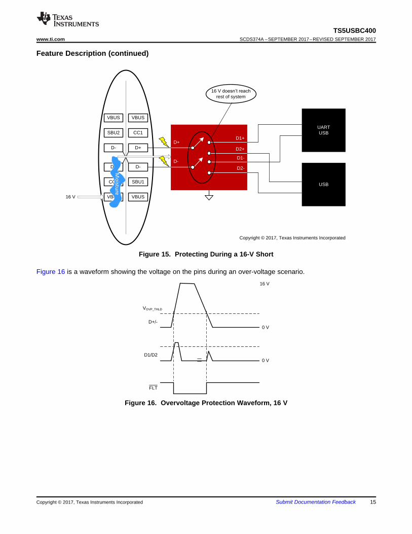
8.3.2 Overvoltage ProtectionThe OVP of the TS5USBC400 is designed to protect the system from D+/- shorts to VBUS at the USB and USBType-C connector. Figure 14 depicts a moisture short that would cause 16 V to appear on an existing USBsolution that could pass through the device and damage components behind the device.
Figure 14. Existing Solution Being Damaged by a Short, 16 V
The TS5USBC400 will open the switches and protect the rest of the system by blocking the 16 V as depicted in .
D+/-
D1/D2
FLT
VOVP_THLD
0 V
0 V
16 V
D+
D2-
D-D1-
D2+
D1+
D+
D-
D-
D+
CC2
CC1UARTUSB
USB
VBUS VBUS
VBUS VBUS
SBU1
SBU2
16 9GRHVQ¶WUHDFKrest of system
Moisture
16 V
Copyright © 2017, Texas Instruments Incorporated
15
TS5USBC400www.ti.com SCDS374A –SEPTEMBER 2017–REVISED SEPTEMBER 2017
Submit Documentation FeedbackCopyright © 2017, Texas Instruments Incorporated
Feature Description (continued)
Figure 15. Protecting During a 16-V Short
Figure 16 is a waveform showing the voltage on the pins during an over-voltage scenario.
Figure 16. Overvoltage Protection Waveform, 16 V

16
TS5USBC400SCDS374A –SEPTEMBER 2017–REVISED SEPTEMBER 2017 www.ti.com
Submit Documentation Feedback Copyright © 2017, Texas Instruments Incorporated
8.4 Device Functional Modes
8.4.1 Pin Functions
Table 1. Function TableOE SEL1 SEL2 D- Connection D+ ConnectionH X X High-Z High-ZL L L D- to D1- D+ to D1+L L H D- to D1- D+ to D2+L H L D- to D2- D+ to D1+L H H D- to D2- D+ to D2+

USB
VCC
D1-
D2+
OVP
LogicControl
GND
VB
US
DP
_TD
P_B
DM
_TD
M_B
GN
D
USBConnector
Copyright © 2017, Texas Instruments Incorporated
UARTUSB
D2-
SEL1
SEL2
OE
FLT
D1+
VCC
100 nF
17
TS5USBC400www.ti.com SCDS374A –SEPTEMBER 2017–REVISED SEPTEMBER 2017
Submit Documentation FeedbackCopyright © 2017, Texas Instruments Incorporated
9 Application and Implementation
NOTEInformation in the following applications sections is not part of the TI componentspecification, and TI does not warrant its accuracy or completeness. TI’s customers areresponsible for determining suitability of components for their purposes. Customers shouldvalidate and test their design implementation to confirm system functionality.
9.1 Application InformationThere are many USB applications in which the USB hubs or controllers have a limited number of USB I/Os orneed to route signals from a single USB connector. The TS5USBC400 solution can effectively expand the limitedUSB I/Os by switching between multiple USB buses to interface them to a single USB hub or controller or routesignals from on connector to two different locations. With independent control of the two switches using SEL1and SEL2, TS5USBC400 can be used to cross switch single ended signals.
9.2 Typical ApplicationTS5USBC400 USB/UART switch. The TS5USBC400 is used to switch signals between the USB path, whichgoes to the baseband or application processor, or the UART path, which goes to debug port. The TS5USBC400has internal 6-MΩ pull-down resistors on SEL1, SEL2, and OE. The pull-down on SEL1 and SEL2 pins ensurethe D1+/D1- channel is selected by default. The pull-down on OE enables the switch when power is applied.
Figure 17. Typical TS5USBC400 Application
9.2.1 Design RequirementsDesign requirements of USB 1.0,1.1, and 2.0 standards must be followed. The TS5USBC400 has internal 6-MΩpulldown resistors on SEL1, SEL2, and OE, so no external resistors are required on the logic pins. The internalpull-down resistor on SEL1 and SEL2 pins ensures the D1+ and D1- channels are selected by default. Theinternal pull-down resistor on OE enables the switch when power is applied to VCC.
9.2.2 Detailed Design ProcedureThe TS5USBC400can be properly operated without any external components. However, TI recommends thatunused pins must be connected to ground through a 50-Ω resistor to prevent signal reflections back into thedevice. TI does recommend a 100nF bypass capacitor placed close to TS5USBC400 VCC pin.

0.0 0.5 1.0 1.5 2.0
-0.2
-0.4
0.0
0.4
0.2
Time (ns)
Diff
eren
tial S
igna
l (V
)
0.0 0.5 1.0 1.5 2.0
-0.2
-0.4
0.0
0.4
0.2
Time (ns)
Diff
eren
tial S
igna
l (V
)
18
TS5USBC400SCDS374A –SEPTEMBER 2017–REVISED SEPTEMBER 2017 www.ti.com
Submit Documentation Feedback Copyright © 2017, Texas Instruments Incorporated
Typical Application (continued)9.2.3 Application Curves
Figure 18. High Speed Eye Diagram With TS5USBC400 Figure 19. High Speed Eye Diagram Without TS5USBC400
10 Power Supply RecommendationsPower to the device is supplied through the VCC pin and must follow the USB 1.0, 1.1, and 2.0 standards. TIrecommends placing a 100nF bypass capacitor as close to the supply pin VCC as possible to help smooth outlower frequency noise to provide better load regulation across the frequency spectrum.

Signal 1
GND Plane
Power Plane
Signal 2
19
TS5USBC400www.ti.com SCDS374A –SEPTEMBER 2017–REVISED SEPTEMBER 2017
Submit Documentation FeedbackCopyright © 2017, Texas Instruments Incorporated
11 Layout
11.1 Layout Guidelines1. Place supply bypass capacitors as close to VCC pin as possible and avoid placing the bypass caps near the
D± traces.2. The high-speed D± must match and be no more than 4 inches long; otherwise, the eye diagram performance
may be degraded. A high-speed USB connection is made through a shielded, twisted pair cable with adifferential characteristic impedance. In layout, the impedance of D+ and D– traces must match the cablecharacteristic differential impedance for optimal performance.
3. Route the high-speed USB signals using a minimum of vias and corners which reduces signal reflections andimpedance changes. When a via must be used, increase the clearance size around it to minimize itscapacitance. Each via introduces discontinuities in the signal’s transmission line and increases the chance ofpicking up interference from the other layers of the board. Be careful when designing test points on twistedpair lines; through-hole pins are not recommended.
4. When it becomes necessary to turn 90°, use two 45° turns or an arc instead of making a single 90° turn. Thisreduces reflections on the signal traces by minimizing impedance discontinuities.
5. Do not route USB traces under or near crystals, oscillators, clock signal generators, switching regulators,mounting holes, magnetic devices or ICs that use or duplicate clock signals.
6. Avoid stubs on the high-speed USB signals because they cause signal reflections. If a stub is unavoidable,then the stub must be less than 200 mm.
7. Route all high-speed USB signal traces over continuous GND planes, with no interruptions.8. Avoid crossing over anti-etch, commonly found with plane splits.9. Due to high frequencies associated with the USB, a printed circuit board with at least four layers is
recommended; two signal layers separated by a ground and power layer as shown in Figure 20.
Figure 20. Four-Layer Board Stack-Up
The majority of signal traces must run on a single layer, preferably Signal 1. Immediately next to this layer mustbe the GND plane, which is solid with no cuts. Avoid running signal traces across a split in the ground or powerplane. When running across split planes is unavoidable, sufficient decoupling must be used. Minimizing thenumber of signal vias reduces EMI by reducing inductance at high frequencies.

C3C2C1
B1
A2A2A1
D+
B2
C4
B4
A3
B3
D-
Top Layer 1 (Signal1)
Inner Layer 2 (GND)
Inner Layer 3 (VCC)
Bottom Layer 4 (Signal2)
Example 4 layer PCB Stackup
Via to layer 2 (GND)
Via to layer 3 (VCC)
D2+ D2- D1+ D1-
Via to layer 4 (Signal)
SEL1
SEL2
VCC
FLT#
OE#
GND
Place near VCC pin.
20
TS5USBC400SCDS374A –SEPTEMBER 2017–REVISED SEPTEMBER 2017 www.ti.com
Submit Documentation Feedback Copyright © 2017, Texas Instruments Incorporated
11.2 Layout Example
Figure 21. Layout Example

21
TS5USBC400www.ti.com SCDS374A –SEPTEMBER 2017–REVISED SEPTEMBER 2017
Submit Documentation FeedbackCopyright © 2017, Texas Instruments Incorporated
12 Device and Documentation Support
12.1 Documentation Support
12.1.1 Related DocumentationFor related documentation see the following:• USB 2.0 Board Design and Layout Guidelines• High-Speed Layout Guidelines Application Report• High-Speed Interface Layout Guidelines
12.2 Community ResourcesThe following links connect to TI community resources. Linked contents are provided "AS IS" by the respectivecontributors. They do not constitute TI specifications and do not necessarily reflect TI's views; see TI's Terms ofUse.
TI E2E™ Online Community TI's Engineer-to-Engineer (E2E) Community. Created to foster collaborationamong engineers. At e2e.ti.com, you can ask questions, share knowledge, explore ideas and helpsolve problems with fellow engineers.
Design Support TI's Design Support Quickly find helpful E2E forums along with design support tools andcontact information for technical support.
12.3 TrademarksE2E is a trademark of Texas Instruments.USB Type-C is a trademark of USB Implementers Forum.All other trademarks are the property of their respective owners.
12.4 Electrostatic Discharge CautionThis integrated circuit can be damaged by ESD. Texas Instruments recommends that all integrated circuits be handled withappropriate precautions. Failure to observe proper handling and installation procedures can cause damage.
ESD damage can range from subtle performance degradation to complete device failure. Precision integrated circuits may be moresusceptible to damage because very small parametric changes could cause the device not to meet its published specifications.
12.5 GlossarySLYZ022 — TI Glossary.
This glossary lists and explains terms, acronyms, and definitions.
13 Mechanical, Packaging, and Orderable InformationThe following pages include mechanical, packaging, and orderable information. This information is the mostcurrent data available for the designated devices. This data is subject to change without notice and revision ofthis document. For browser-based versions of this data sheet, refer to the left-hand navigation.

www.ti.com
PACKAGE OUTLINE
C0.5 MAX
0.190.13
0.8
TYP
1.2 TYP
0.4 TYP
0.4
TYP
12X0.250.21
B1.6121.552 A
1.2121.152
4223498/B 04/2017
DSBGA - 0.5 mm max heightYFP0012-C01DIE SIZE BALL GRID ARRAY
NOTES:
1. All linear dimensions are in millimeters. Any dimensions in parenthesis are for reference only. Dimensioning and tolerancingper ASME Y14.5M.
2. This drawing is subject to change without notice.
BALL A1CORNER
SEATING PLANE
BALL TYP 0.05 C
A
B
C
1 2 3
0.015 C A B
SYMM
SYMM
4
SCALE 8.000
22
TS5USBC400SCDS374A –SEPTEMBER 2017–REVISED SEPTEMBER 2017 www.ti.com
Submit Documentation Feedback Copyright © 2017, Texas Instruments Incorporated
www.ti.com
EXAMPLE BOARD LAYOUT
12X ( 0.23)
(0.4) TYP
(0.4) TYP
( 0.23)METAL
0.05 MAX
SOLDER MASKOPENING
METAL UNDERSOLDER MASK
( 0.23)SOLDER MASKOPENING
0.05 MIN
4223498/B 04/2017
DSBGA - 0.5 mm max heightYFP0012-C01DIE SIZE BALL GRID ARRAY
NOTES: (continued)
3. Final dimensions may vary due to manufacturing tolerance considerations and also routing constraints.For more information, see Texas Instruments literature number SNVA009 (www.ti.com/lit/snva009).
SYMM
SYMM
LAND PATTERN EXAMPLEEXPOSED METAL SHOWN
SCALE:50X
A
B
C
1 2 3 4
NON-SOLDER MASKDEFINED
(PREFERRED)
NOT TO SCALESOLDER MASK DETAILS
EXPOSEDMETAL
SOLDER MASKDEFINED
EXPOSEDMETAL
23
TS5USBC400www.ti.com SCDS374A –SEPTEMBER 2017–REVISED SEPTEMBER 2017
Submit Documentation FeedbackCopyright © 2017, Texas Instruments Incorporated

www.ti.com
EXAMPLE STENCIL DESIGN
(0.4) TYP
(0.4) TYP
12X ( 0.25) (R0.05) TYP
METALTYP
4223498/B 04/2017
DSBGA - 0.5 mm max heightYFP0012-C01DIE SIZE BALL GRID ARRAY
NOTES: (continued)
4. Laser cutting apertures with trapezoidal walls and rounded corners may offer better paste release.
SYMM
SYMM
SOLDER PASTE EXAMPLEBASED ON 0.1 mm THICK STENCIL
SCALE:50X
A
B
C
1 2 3 4
24
TS5USBC400SCDS374A –SEPTEMBER 2017–REVISED SEPTEMBER 2017 www.ti.com
Submit Documentation Feedback Copyright © 2017, Texas Instruments Incorporated

PACKAGE OPTION ADDENDUM
www.ti.com 6-Oct-2017
Addendum-Page 1
PACKAGING INFORMATION
Orderable Device Status(1)
Package Type PackageDrawing
Pins PackageQty
Eco Plan(2)
Lead/Ball Finish(6)
MSL Peak Temp(3)
Op Temp (°C) Device Marking(4/5)
Samples
TS5USBC400IYFPR ACTIVE DSBGA YFP 12 3000 Green (RoHS& no Sb/Br)
SNAGCU Level-1-260C-UNLIM -40 to 85 USB4
TS5USBC400IYFPT ACTIVE DSBGA YFP 12 250 Green (RoHS& no Sb/Br)
SNAGCU Level-1-260C-UNLIM -40 to 85 USB4
TS5USBC400YFPR ACTIVE DSBGA YFP 12 3000 Green (RoHS& no Sb/Br)
SNAGCU Level-1-260C-UNLIM 0 to 70 USB4
TS5USBC400YFPT ACTIVE DSBGA YFP 12 250 Green (RoHS& no Sb/Br)
SNAGCU Level-1-260C-UNLIM 0 to 70 USB4
(1) The marketing status values are defined as follows:ACTIVE: Product device recommended for new designs.LIFEBUY: TI has announced that the device will be discontinued, and a lifetime-buy period is in effect.NRND: Not recommended for new designs. Device is in production to support existing customers, but TI does not recommend using this part in a new design.PREVIEW: Device has been announced but is not in production. Samples may or may not be available.OBSOLETE: TI has discontinued the production of the device.
(2) RoHS: TI defines "RoHS" to mean semiconductor products that are compliant with the current EU RoHS requirements for all 10 RoHS substances, including the requirement that RoHS substancedo not exceed 0.1% by weight in homogeneous materials. Where designed to be soldered at high temperatures, "RoHS" products are suitable for use in specified lead-free processes. TI mayreference these types of products as "Pb-Free".RoHS Exempt: TI defines "RoHS Exempt" to mean products that contain lead but are compliant with EU RoHS pursuant to a specific EU RoHS exemption.Green: TI defines "Green" to mean the content of Chlorine (Cl) and Bromine (Br) based flame retardants meet JS709B low halogen requirements of <=1000ppm threshold. Antimony trioxide basedflame retardants must also meet the <=1000ppm threshold requirement.
(3) MSL, Peak Temp. - The Moisture Sensitivity Level rating according to the JEDEC industry standard classifications, and peak solder temperature.
(4) There may be additional marking, which relates to the logo, the lot trace code information, or the environmental category on the device.
(5) Multiple Device Markings will be inside parentheses. Only one Device Marking contained in parentheses and separated by a "~" will appear on a device. If a line is indented then it is a continuationof the previous line and the two combined represent the entire Device Marking for that device.
(6) Lead/Ball Finish - Orderable Devices may have multiple material finish options. Finish options are separated by a vertical ruled line. Lead/Ball Finish values may wrap to two lines if the finishvalue exceeds the maximum column width.
Important Information and Disclaimer:The information provided on this page represents TI's knowledge and belief as of the date that it is provided. TI bases its knowledge and belief on informationprovided by third parties, and makes no representation or warranty as to the accuracy of such information. Efforts are underway to better integrate information from third parties. TI has taken and

PACKAGE OPTION ADDENDUM
www.ti.com 6-Oct-2017
Addendum-Page 2
continues to take reasonable steps to provide representative and accurate information but may not have conducted destructive testing or chemical analysis on incoming materials and chemicals.TI and TI suppliers consider certain information to be proprietary, and thus CAS numbers and other limited information may not be available for release.
In no event shall TI's liability arising out of such information exceed the total purchase price of the TI part(s) at issue in this document sold by TI to Customer on an annual basis.

TAPE AND REEL INFORMATION
*All dimensions are nominal
Device PackageType
PackageDrawing
Pins SPQ ReelDiameter
(mm)
ReelWidth
W1 (mm)
A0(mm)
B0(mm)
K0(mm)
P1(mm)
W(mm)
Pin1Quadrant
TS5USBC400IYFPR DSBGA YFP 12 3000 180.0 8.4 1.32 1.72 0.62 4.0 8.0 Q2
TS5USBC400IYFPT DSBGA YFP 12 250 180.0 8.4 1.32 1.72 0.62 4.0 8.0 Q2
TS5USBC400YFPR DSBGA YFP 12 3000 180.0 8.4 1.32 1.72 0.62 4.0 8.0 Q2
TS5USBC400YFPT DSBGA YFP 12 250 180.0 8.4 1.32 1.72 0.62 4.0 8.0 Q2
PACKAGE MATERIALS INFORMATION
www.ti.com 9-Mar-2018
Pack Materials-Page 1

*All dimensions are nominal
Device Package Type Package Drawing Pins SPQ Length (mm) Width (mm) Height (mm)
TS5USBC400IYFPR DSBGA YFP 12 3000 182.0 182.0 20.0
TS5USBC400IYFPT DSBGA YFP 12 250 182.0 182.0 20.0
TS5USBC400YFPR DSBGA YFP 12 3000 182.0 182.0 20.0
TS5USBC400YFPT DSBGA YFP 12 250 182.0 182.0 20.0
PACKAGE MATERIALS INFORMATION
www.ti.com 9-Mar-2018
Pack Materials-Page 2

IMPORTANT NOTICE
Texas Instruments Incorporated (TI) reserves the right to make corrections, enhancements, improvements and other changes to itssemiconductor products and services per JESD46, latest issue, and to discontinue any product or service per JESD48, latest issue. Buyersshould obtain the latest relevant information before placing orders and should verify that such information is current and complete.TI’s published terms of sale for semiconductor products (http://www.ti.com/sc/docs/stdterms.htm) apply to the sale of packaged integratedcircuit products that TI has qualified and released to market. Additional terms may apply to the use or sale of other types of TI products andservices.Reproduction of significant portions of TI information in TI data sheets is permissible only if reproduction is without alteration and isaccompanied by all associated warranties, conditions, limitations, and notices. TI is not responsible or liable for such reproduceddocumentation. Information of third parties may be subject to additional restrictions. Resale of TI products or services with statementsdifferent from or beyond the parameters stated by TI for that product or service voids all express and any implied warranties for theassociated TI product or service and is an unfair and deceptive business practice. TI is not responsible or liable for any such statements.Buyers and others who are developing systems that incorporate TI products (collectively, “Designers”) understand and agree that Designersremain responsible for using their independent analysis, evaluation and judgment in designing their applications and that Designers havefull and exclusive responsibility to assure the safety of Designers' applications and compliance of their applications (and of all TI productsused in or for Designers’ applications) with all applicable regulations, laws and other applicable requirements. Designer represents that, withrespect to their applications, Designer has all the necessary expertise to create and implement safeguards that (1) anticipate dangerousconsequences of failures, (2) monitor failures and their consequences, and (3) lessen the likelihood of failures that might cause harm andtake appropriate actions. Designer agrees that prior to using or distributing any applications that include TI products, Designer willthoroughly test such applications and the functionality of such TI products as used in such applications.TI’s provision of technical, application or other design advice, quality characterization, reliability data or other services or information,including, but not limited to, reference designs and materials relating to evaluation modules, (collectively, “TI Resources”) are intended toassist designers who are developing applications that incorporate TI products; by downloading, accessing or using TI Resources in anyway, Designer (individually or, if Designer is acting on behalf of a company, Designer’s company) agrees to use any particular TI Resourcesolely for this purpose and subject to the terms of this Notice.TI’s provision of TI Resources does not expand or otherwise alter TI’s applicable published warranties or warranty disclaimers for TIproducts, and no additional obligations or liabilities arise from TI providing such TI Resources. TI reserves the right to make corrections,enhancements, improvements and other changes to its TI Resources. TI has not conducted any testing other than that specificallydescribed in the published documentation for a particular TI Resource.Designer is authorized to use, copy and modify any individual TI Resource only in connection with the development of applications thatinclude the TI product(s) identified in such TI Resource. NO OTHER LICENSE, EXPRESS OR IMPLIED, BY ESTOPPEL OR OTHERWISETO ANY OTHER TI INTELLECTUAL PROPERTY RIGHT, AND NO LICENSE TO ANY TECHNOLOGY OR INTELLECTUAL PROPERTYRIGHT OF TI OR ANY THIRD PARTY IS GRANTED HEREIN, including but not limited to any patent right, copyright, mask work right, orother intellectual property right relating to any combination, machine, or process in which TI products or services are used. Informationregarding or referencing third-party products or services does not constitute a license to use such products or services, or a warranty orendorsement thereof. Use of TI Resources may require a license from a third party under the patents or other intellectual property of thethird party, or a license from TI under the patents or other intellectual property of TI.TI RESOURCES ARE PROVIDED “AS IS” AND WITH ALL FAULTS. TI DISCLAIMS ALL OTHER WARRANTIES ORREPRESENTATIONS, EXPRESS OR IMPLIED, REGARDING RESOURCES OR USE THEREOF, INCLUDING BUT NOT LIMITED TOACCURACY OR COMPLETENESS, TITLE, ANY EPIDEMIC FAILURE WARRANTY AND ANY IMPLIED WARRANTIES OFMERCHANTABILITY, FITNESS FOR A PARTICULAR PURPOSE, AND NON-INFRINGEMENT OF ANY THIRD PARTY INTELLECTUALPROPERTY RIGHTS. TI SHALL NOT BE LIABLE FOR AND SHALL NOT DEFEND OR INDEMNIFY DESIGNER AGAINST ANY CLAIM,INCLUDING BUT NOT LIMITED TO ANY INFRINGEMENT CLAIM THAT RELATES TO OR IS BASED ON ANY COMBINATION OFPRODUCTS EVEN IF DESCRIBED IN TI RESOURCES OR OTHERWISE. IN NO EVENT SHALL TI BE LIABLE FOR ANY ACTUAL,DIRECT, SPECIAL, COLLATERAL, INDIRECT, PUNITIVE, INCIDENTAL, CONSEQUENTIAL OR EXEMPLARY DAMAGES INCONNECTION WITH OR ARISING OUT OF TI RESOURCES OR USE THEREOF, AND REGARDLESS OF WHETHER TI HAS BEENADVISED OF THE POSSIBILITY OF SUCH DAMAGES.Unless TI has explicitly designated an individual product as meeting the requirements of a particular industry standard (e.g., ISO/TS 16949and ISO 26262), TI is not responsible for any failure to meet such industry standard requirements.Where TI specifically promotes products as facilitating functional safety or as compliant with industry functional safety standards, suchproducts are intended to help enable customers to design and create their own applications that meet applicable functional safety standardsand requirements. Using products in an application does not by itself establish any safety features in the application. Designers mustensure compliance with safety-related requirements and standards applicable to their applications. Designer may not use any TI products inlife-critical medical equipment unless authorized officers of the parties have executed a special contract specifically governing such use.Life-critical medical equipment is medical equipment where failure of such equipment would cause serious bodily injury or death (e.g., lifesupport, pacemakers, defibrillators, heart pumps, neurostimulators, and implantables). Such equipment includes, without limitation, allmedical devices identified by the U.S. Food and Drug Administration as Class III devices and equivalent classifications outside the U.S.TI may expressly designate certain products as completing a particular qualification (e.g., Q100, Military Grade, or Enhanced Product).Designers agree that it has the necessary expertise to select the product with the appropriate qualification designation for their applicationsand that proper product selection is at Designers’ own risk. Designers are solely responsible for compliance with all legal and regulatoryrequirements in connection with such selection.Designer will fully indemnify TI and its representatives against any damages, costs, losses, and/or liabilities arising out of Designer’s non-compliance with the terms and provisions of this Notice.
Mailing Address: Texas Instruments, Post Office Box 655303, Dallas, Texas 75265Copyright © 2018, Texas Instruments Incorporated


![Index [] · 2015-01-08 · mcz ovp cl 48vuc 1,25a 8449040000 b.115 mcz ovp cl fg 24vuc 0,5a 8704240000 b.118 mcz ovp filter 24v 0,5a 8449100000 b.119 mcz ovp gasableiter 90v 8449130000](https://static.fdocuments.us/doc/165x107/5e96e66af12683124d138cf4/index-2015-01-08-mcz-ovp-cl-48vuc-125a-8449040000-b115-mcz-ovp-cl-fg-24vuc.jpg)