TS 136 212 - V10.6.0 - LTE; Evolved Universal Terrestrial - ETSI

ETSI TS 125 104 V10.6.0 (2012-07)
Universal Mobile Telecommunications System (UMTS); Base Station (BS) radio transmission and reception (FDD)
(3GPP TS 25.104 version 10.6.0 Release 10)
Technical Specification

ETSI
ETSI TS 125 104 V10.6.0 (2012-07)13GPP TS 25.104 version 10.6.0 Release 10
Reference RTS/TSGR-0425104va60
Keywords UMTS
ETSI
650 Route des Lucioles F-06921 Sophia Antipolis Cedex - FRANCE
Tel.: +33 4 92 94 42 00 Fax: +33 4 93 65 47 16
Siret N° 348 623 562 00017 - NAF 742 C
Association à but non lucratif enregistrée à la Sous-Préfecture de Grasse (06) N° 7803/88
Important notice
Individual copies of the present document can be downloaded from: http://www.etsi.org
The present document may be made available in more than one electronic version or in print. In any case of existing or perceived difference in contents between such versions, the reference version is the Portable Document Format (PDF).
In case of dispute, the reference shall be the printing on ETSI printers of the PDF version kept on a specific network drive within ETSI Secretariat.
Users of the present document should be aware that the document may be subject to revision or change of status. Information on the current status of this and other ETSI documents is available at
http://portal.etsi.org/tb/status/status.asp
If you find errors in the present document, please send your comment to one of the following services: http://portal.etsi.org/chaircor/ETSI_support.asp
Copyright Notification
No part may be reproduced except as authorized by written permission. The copyright and the foregoing restriction extend to reproduction in all media.
© European Telecommunications Standards Institute 2012.
All rights reserved.
DECTTM, PLUGTESTSTM, UMTSTM and the ETSI logo are Trade Marks of ETSI registered for the benefit of its Members. 3GPPTM and LTE™ are Trade Marks of ETSI registered for the benefit of its Members and
of the 3GPP Organizational Partners. GSM® and the GSM logo are Trade Marks registered and owned by the GSM Association.

ETSI
ETSI TS 125 104 V10.6.0 (2012-07)23GPP TS 25.104 version 10.6.0 Release 10
Intellectual Property Rights IPRs essential or potentially essential to the present document may have been declared to ETSI. The information pertaining to these essential IPRs, if any, is publicly available for ETSI members and non-members, and can be found in ETSI SR 000 314: "Intellectual Property Rights (IPRs); Essential, or potentially Essential, IPRs notified to ETSI in respect of ETSI standards", which is available from the ETSI Secretariat. Latest updates are available on the ETSI Web server (http://ipr.etsi.org).
Pursuant to the ETSI IPR Policy, no investigation, including IPR searches, has been carried out by ETSI. No guarantee can be given as to the existence of other IPRs not referenced in ETSI SR 000 314 (or the updates on the ETSI Web server) which are, or may be, or may become, essential to the present document.
Foreword This Technical Specification (TS) has been produced by ETSI 3rd Generation Partnership Project (3GPP).
The present document may refer to technical specifications or reports using their 3GPP identities, UMTS identities or GSM identities. These should be interpreted as being references to the corresponding ETSI deliverables.
The cross reference between GSM, UMTS, 3GPP and ETSI identities can be found under http://webapp.etsi.org/key/queryform.asp.

ETSI
ETSI TS 125 104 V10.6.0 (2012-07)33GPP TS 25.104 version 10.6.0 Release 10
Contents
Intellectual Property Rights ................................................................................................................................ 2
Foreword ............................................................................................................................................................. 2
Foreword ............................................................................................................................................................. 7
1 Scope ........................................................................................................................................................ 8
2 References ................................................................................................................................................ 8
3 Definitions and abbreviations ................................................................................................................... 8
3.1 Definitions .......................................................................................................................................................... 8
3.2 Abbreviations ..................................................................................................................................................... 9
4 General ................................................................................................................................................... 10
4.1 Relationship between Minimum Requirements and Test Requirements .......................................................... 10
4.2 Base station classes .......................................................................................................................................... 10
4.3 Regional requirements ...................................................................................................................................... 11
4.4 Environmental requirements for the BS equipment ......................................................................................... 12
4.5 Applicability of requirements ........................................................................................................................... 12
5 Frequency bands and channel arrangement ............................................................................................ 12
5.1 General ............................................................................................................................................................. 12
5.2 Frequency bands ............................................................................................................................................... 13
5.3 Tx-Rx frequency separation ............................................................................................................................. 14
5.4 Channel arrangement ........................................................................................................................................ 15
5.4.1 Channel spacing .......................................................................................................................................... 15
5.4.2 Channel raster ............................................................................................................................................. 15
5.4.3 Channel number .......................................................................................................................................... 15
6 Transmitter characteristics ..................................................................................................................... 16
6.1 General ............................................................................................................................................................. 16
6.2 Base station output power ................................................................................................................................ 17
6.2.1 Base station maximum output power .......................................................................................................... 17
6.2.1.1 Minimum requirement .......................................................................................................................... 17
6.3 Frequency error ................................................................................................................................................ 17
6.3.1 Minimum requirement ................................................................................................................................ 18
6.4 Output power dynamics .................................................................................................................................... 18
6.4.1 Inner loop power control in the downlink ................................................................................................... 18
6.4.1.1 Power control steps ............................................................................................................................... 18
6.4.1.1.1 Minimum requirement ..................................................................................................................... 18
6.4.2 Power control dynamic range ..................................................................................................................... 19
6.4.2.1 Minimum requirements ......................................................................................................................... 19
6.4.3 Total power dynamic range ........................................................................................................................ 19
6.4.3.1 Minimum requirement .......................................................................................................................... 19
6.4.4 Primary CPICH power ................................................................................................................................ 19
6.4.4.1 Minimum requirement .......................................................................................................................... 19
6.4.4A Secondary CPICH power ............................................................................................................................ 19
6.4.4A.1 Minimum Requirement ...................................................................................................................................... 19
6.4.5 IPDL time mask .......................................................................................................................................... 19
6.4.5.1 Minimum Requirement ......................................................................................................................... 20
6.4.6 Home base station output power for adjacent channel protection ............................................................... 20
6.4.6.1 Minimum requirement .......................................................................................................................... 21
6.5 (void) ................................................................................................................................................................ 21
6.6 Output RF spectrum emissions ......................................................................................................................... 21
6.6.1 Occupied bandwidth ................................................................................................................................... 21
6.6.1.1 Minimum requirement .......................................................................................................................... 21
6.6.2 Out of band emission .................................................................................................................................. 21
6.6.2.1 Spectrum emission mask ....................................................................................................................... 22
6.6.2.2 Adjacent Channel Leakage power Ratio (ACLR) ................................................................................. 25
ETSI
ETSI TS 125 104 V10.6.0 (2012-07)43GPP TS 25.104 version 10.6.0 Release 10
6.6.2.2.1 Minimum requirement ..................................................................................................................... 25
6.6.3 Spurious emissions ..................................................................................................................................... 25
6.6.3.1 Mandatory Requirements ...................................................................................................................... 26
6.6.3.1.1 Spurious emissions (Category A) .................................................................................................... 26
6.6.3.1.2 Spurious emissions (Category B) .................................................................................................... 26
6.6.3.2 Protection of the BS receiver of own or different BS ........................................................................... 28
6.6.3.2.1 Minimum Requirement ................................................................................................................... 28
6.6.3.3 Co-existence with other systems in the same geographical area ........................................................... 30
6.6.3.3.1 Minimum Requirements .................................................................................................................. 31
6.6.3.4 Co-existence with co-located and co-sited base stations ....................................................................... 33
6.6.3.4.1 Minimum Requirements .................................................................................................................. 34
6.6.3.5 Co-existence with PHS ......................................................................................................................... 37
6.6.3.5.1 Minimum Requirement ................................................................................................................... 37
6.6.3.6 Co-existence with services in adjacent frequency bands....................................................................... 37
6.6.3.6.1 Minimum requirement ..................................................................................................................... 37
6.6.3.7 Void....................................................................................................................................................... 38
6.6.3.7.1 Void ................................................................................................................................................. 38
6.6.3.7.2 Void ................................................................................................................................................. 38
6.6.3.8 Protection of Public Safety Operations ................................................................................................. 38
6.6.3.8.1 Minimum Requirement ................................................................................................................... 38
6.6.3.9 Co-existence with Home BS operating in other bands .......................................................................... 38
6.6.3.9.1 Minimum Requirements .................................................................................................................. 39
6.7 Transmit intermodulation ................................................................................................................................. 40
6.7.1 Minimum requirement ................................................................................................................................ 40
6.8 Transmit modulation ........................................................................................................................................ 40
6.8.1 Transmit pulse shape filter .......................................................................................................................... 40
6.8.2 Error Vector Magnitude .............................................................................................................................. 41
6.8.2.1 Minimum requirement .......................................................................................................................... 41
6.8.3 Peak code Domain error ............................................................................................................................. 41
6.8.3.1 Minimum requirement .......................................................................................................................... 41
6.8.4 Time alignment error .................................................................................................................................. 41
6.8.4.1 Minimum Requirements ........................................................................................................................ 41
6.8.5 Relative Code Domain Error for 64QAM modulation............................................................................... 41
6.8.5.1 Minimum requirement .......................................................................................................................... 42
7 Receiver characteristics .......................................................................................................................... 42
7.1 General ............................................................................................................................................................. 42
7.2 Reference sensitivity level ................................................................................................................................ 42
7.2.1 Minimum requirement ................................................................................................................................ 43
7.2.2 Maximum Frequency Deviation for Receiver Performance ....................................................................... 43
7.3 Dynamic range ................................................................................................................................................. 43
7.3.1 Minimum requirement ................................................................................................................................ 43
7.4 Adjacent Channel Selectivity (ACS) ................................................................................................................ 43
7.4.1 Minimum requirement ................................................................................................................................ 44
7.4.2 Minimum requirement - Co-location with UTRA-TDD ............................................................................. 44
7.5 Blocking characteristics ................................................................................................................................... 44
7.5.1 Minimum requirement ................................................................................................................................ 45
7.5.2 Minimum Requirement - Co-location with GSM, DCS, PCS, CDMA, UTRA and/or E-UTRA, UTRA TDD and/or E-UTRA TDD ............................................................................................................ 51
7.5.3 Void ............................................................................................................................................................ 55
7.6 Intermodulation characteristics ........................................................................................................................ 55
7.6.1 Minimum requirement ................................................................................................................................ 55
7.7 Spurious emissions ........................................................................................................................................... 56
7.7.1 Minimum requirement ................................................................................................................................ 57
8 Performance requirement ....................................................................................................................... 57
8.1 General ............................................................................................................................................................. 57
8.2 Demodulation in static propagation conditions ................................................................................................ 58
8.2.1 Demodulation of DCH ................................................................................................................................ 58
8.2.1.1 Minimum requirement .......................................................................................................................... 58
8.3 Demodulation of DCH in multipath fading conditions .................................................................................... 59
8.3.1 Multipath fading Case 1 .............................................................................................................................. 59

ETSI
ETSI TS 125 104 V10.6.0 (2012-07)53GPP TS 25.104 version 10.6.0 Release 10
8.3.1.1 Minimum requirement .......................................................................................................................... 59
8.3.2 Multipath fading Case 2 .............................................................................................................................. 59
8.3.2.1 Minimum requirement .......................................................................................................................... 59
8.3.3 Multipath fading Case 3 .............................................................................................................................. 60
8.3.3.1 Minimum requirement .......................................................................................................................... 60
8.3.4 Multipath fading Case 4 .............................................................................................................................. 60
8.3.4.1 Minimum requirement .......................................................................................................................... 61
8.4 Demodulation of DCH in moving propagation conditions ............................................................................... 61
8.4.1 Minimum requirement ................................................................................................................................ 61
8.5 Demodulation of DCH in birth/death propagation conditions .......................................................................... 61
8.5.1 Minimum requirement ................................................................................................................................ 62
8.5A Demodulation of DCH in high speed train conditions ..................................................................................... 62
8.5A.1 General ........................................................................................................................................................ 62
8.5A.2 Minimum requirement ................................................................................................................................ 62
8.6 (void) ................................................................................................................................................................ 62
8.7 Performance requirement for RACH ................................................................................................................ 62
8.7.1 Performance requirement for RACH preamble detection ........................................................................... 62
8.7.2 Demodulation of RACH message ............................................................................................................... 63
8.7.2.1 Minimum requirements for Static Propagation Condition .................................................................... 63
8.7.2.2 Minimum requirements for Multipath Fading Case 3 ........................................................................... 64
8.7.2.3 Minimum requirements for high speed train conditions ....................................................................... 64
8.8 (void) ................................................................................................................................................................ 65
8.9 (void) ................................................................................................................................................................ 65
8.10 Performance of ACK/NACK detection for HS-DPCCH .................................................................................. 65
8.10.1 ACK false alarm ......................................................................................................................................... 65
8.10.2 ACK mis-detection ..................................................................................................................................... 65
8.10A Performance of ACK/NACK detection for 4C-HSDPA HS-DPCCH .............................................................. 65
8.10A.1 Performance requirements .......................................................................................................................... 66
8.10A.1.1 ACK false alarm .................................................................................................................................... 66
8.10A.1.2 ACK mis-detection................................................................................................................................ 66
8.10A.2 Applicability of requirements ..................................................................................................................... 67
8.11 Demodulation of E-DPDCH in multipath fading condition ............................................................................. 67
8.12 Performance of signaling detection for E-DPCCH in multipath fading condition ........................................... 68
Annex A (normative): Measurement channels .................................................................................. 70
A.1 Summary of UL reference measurement channels ................................................................................. 70
A.2 UL reference measurement channel for 12.2 kbps ................................................................................. 71
A.3 UL reference measurement channel for 64 kbps .................................................................................... 72
A.4 UL reference measurement channel for 144 kbps .................................................................................. 73
A.5 UL reference measurement channel for 384 kbps .................................................................................. 74
A.6 (void) ...................................................................................................................................................... 74
A.7 Reference measurement channels for UL RACH .................................................................................. 75
A.8 Reference measurement channel for HS-DPCCH .................................................................................. 75
A.8A Reference measurement channel for HS-DPCCH for 4C-HSDPA ........................................................ 76
A.9 Summary of E-DPDCH Fixed reference channels ................................................................................. 77
A.10 E-DPDCH Fixed reference channel 1 (FRC1) ....................................................................................... 77
A.11 E-DPDCH Fixed reference channel 2 (FRC2) ....................................................................................... 78
A.12 E-DPDCH Fixed reference channel 3 (FRC3) ....................................................................................... 79
A.13 E-DPDCH Fixed reference channel 4 (FRC4) ....................................................................................... 80
A.14 E-DPDCH Fixed reference channel 5 (FRC5) ....................................................................................... 81
A.15 E-DPDCH Fixed reference channel 6 (FRC6) ....................................................................................... 82

ETSI
ETSI TS 125 104 V10.6.0 (2012-07)63GPP TS 25.104 version 10.6.0 Release 10
A.16 E-DPDCH Fixed reference channel 7 (FRC7) ....................................................................................... 82
A.17 E-DPDCH Fixed reference channel 8 (FRC8) ....................................................................................... 83
Annex B (normative): Propagation conditions .................................................................................. 85
B.1 Static propagation condition ................................................................................................................... 85
B.2 Multi-path fading propagation conditions .............................................................................................. 85
B.3 Moving propagation conditions .............................................................................................................. 85
B.4 Birth-Death propagation conditions ....................................................................................................... 86
B.4A High speed train conditions .................................................................................................................... 87
B.5 Multipath fading propagation conditions for E-DPDCH and E-DPCCH ............................................... 89
Annex C (normative): Characteristics of the W-CDMA interference signal .................................. 90
Annex D (normative): Regional requirement for protection of DTT .............................................. 91
Annex E (informative): Change History .............................................................................................. 92
History .............................................................................................................................................................. 95

ETSI
ETSI TS 125 104 V10.6.0 (2012-07)73GPP TS 25.104 version 10.6.0 Release 10
Foreword This Technical Specification has been produced by the 3GPP.
The contents of the present document are subject to continuing work within the TSG and may change following formal TSG approval. Should the TSG modify the contents of this TS, it will be re-released by the TSG with an identifying change of release date and an increase in version number as follows:
Version 3.y.z
where:
x the first digit:
1 presented to TSG for information;
2 presented to TSG for approval;
3 Indicates TSG approved document under change control.
y the second digit is incremented for all changes of substance, i.e. technical enhancements, corrections, updates, etc.
z the third digit is incremented when editorial only changes have been incorporated in the specification.

ETSI
ETSI TS 125 104 V10.6.0 (2012-07)83GPP TS 25.104 version 10.6.0 Release 10
1 Scope This document establishes the Base Station minimum RF characteristics of the FDD mode of UTRA.
2 References The following documents contain provisions which, through reference in this text, constitute provisions of the present document.
● References are either specific (identified by date of publication, edition number, version number, etc.) or non-specific.
● For a specific reference, subsequent revisions do not apply.
● For a non-specific reference, the latest version applies. In the case of a reference to a 3GPP document (including a GSM document), a non-specific reference implicitly refers to the latest version of that document in the same Release as the present document.
[1] ITU-R Recommendation SM.329, " Unwanted emissions in the spurious domain ".
[2] (void)
[3] ETSI ETR 273-1-2: "Electromagnetic compatibility and Radio spectrum Matters (ERM); Improvement of radiated methods of measurement (using test sites) and evaluation of the corresponding measurement uncertainties; Part 1: Uncertainties in the measurement of mobile radio equipment characteristics; Sub-part 2: Examples and annexes".
[4] 3GPP TR 25.942 "RF System Scenarios".
[5] 3GPP TS 45.004: "Digital cellular telecommunications system (Phase 2+); Modulation".
[6] 3GPP TS 25.213: "Spreading and modulation (FDD)".
[7] ITU-R recommendation SM.328: "Spectra and bandwidth of emissions".
[8] 3GPP TS 36.104: " Evolved Universal Terrestrial Radio Access (E-UTRA); Base Station (BS) radio transmission and reception".
[9] ECC/DEC/(09)03 " Harmonised conditions for MFCN in the band 790-862 MHz", 30 Oct. 2009
[10] 3GPP TS 37.104: " E-UTRA, UTRA and GSM/EDGE; Multi-Standard Radio (MSR) Base Station (BS) radio transmission and reception".
[11] 3GPP TS 25.331: " Radio Resource Control. Protocol Specification".
[12] 3GPP TS 25.214: "Physical layer procedures (FDD) ".
3 Definitions and abbreviations
3.1 Definitions For the purposes of the present document, the following definitions apply:
Output power: The mean power of one carrier of the base station, delivered to a load with resistance equal to the nominal load impedance of the transmitter.
Rated output power: Rated output power of the base station is the mean power level per carrier that the manufacturer has declared to be available at the antenna connector.

ETSI
ETSI TS 125 104 V10.6.0 (2012-07)93GPP TS 25.104 version 10.6.0 Release 10
Maximum output Power: The mean power level per carrier of the base station measured at the antenna connector in a specified reference condition.
Mean power: When applied to a W-CDMA modulated signal this is the power (transmitted or received) in a bandwidth of at least (1+ α) times the chip rate of the radio access mode. The period of measurement shall be at least one timeslot unless otherwise stated.
Power control dynamic range: The difference between the maximum and the minimum transmit output power of a code channel for a specified reference condition.
RRC filtered mean power: The mean power as measured through a root raised cosine filter with roll-off factor α and a bandwidth equal to the chip rate of the radio access mode.
NOTE 1: The RRC filtered mean power of a perfectly modulated W-CDMA signal is 0.246 dB lower than the mean power of the same signal.
Code domain power: That part of the mean power which correlates with a particular (OVSF) code channel. The sum of all powers in the code domain equals the mean power in a bandwidth of (1+ α) times the chip rate of the radio access mode.
Total power dynamic range: The difference between the maximum and the minimum total transmit output power for a specified reference condition.
NOTE 2: The roll-off factor α is defined in section 6.8.1.
Secondary serving HS-DSCH cell(s): In addition to the serving HS-DSCH cell, the set of cells where the UE is configured to simultaneously monitor an HS-SCCH set and receive the HS-DSCH if it is scheduled in that cell. There can be up to 3 secondary serving HS-DSCH cells.
3.2 Abbreviations For the purposes of the present document, the following abbreviations apply:
4C-HSDPA Four-Carrier HSDPA. HSDPA operation configured on 3 or 4 DL carriers 16QAM 16 Quadrature Amplitude Modulation ACIR Adjacent Channel Interference Ratio ACLR Adjacent Channel Leakage power Ratio ACS Adjacent Channel Selectivity BS Base Station BER Bit Error Ratio BLER Block Error Ratio CPICH Common Pilot Channel CW Continuous Wave (unmodulated signal) DB-DC-HSDPA Dual Band Dual Cell HSDPA DC-HSDPA Dual Cell HSDPA DC-HSUPA Dual Cell HSUPA DL Down Link (forward link) DTT Digital Terrestrial Television FDD Frequency Division Duplexing GSM Global System for Mobile Communications HSDPA High Speed Downlink Packet Access HSUPA High Speed Uplink Packet Access IE Information Element MIMO Multiple Input Multiple Output Pout Output Power PRAT Rated Output Power P-CPICH Primary CPICH PHS Personal Handyphone System PPM Parts Per Million RAT Radio Access Technology QPSK Quadrature Phase Shift Keying RSSI Received Signal Strength Indicator

ETSI
ETSI TS 125 104 V10.6.0 (2012-07)103GPP TS 25.104 version 10.6.0 Release 10
S-CPICH Secondary CPICH SIR Signal to Interference ratio TDD Time Division Duplexing TPC Transmit Power Control UARFCN UTRA Absolute Radio Frequency Channel Number UE User Equipment UL Up Link (reverse link) WCDMA Wideband Code Division Multiple Access
4 General
4.1 Relationship between Minimum Requirements and Test Requirements
The Minimum Requirements given in this specification make no allowance for measurement uncertainty. The test specification 25.141 section 4 defines Test Tolerances. These Test Tolerances are individually calculated for each test. The Test Tolerances are used to relax the Minimum Requirements in this specification to create Test Requirements.
The measurement results returned by the Test System are compared - without any modification - against the Test Requirements as defined by the shared risk principle.
The Shared Risk principle is defined in ETR 273 Part 1 sub-part 2 section 6.5.
4.2 Base station classes The requirements in this specification apply to Wide Area Base Stations, Medium Range Base Stations, Local Area Base Stations and Home Base Stations unless otherwise stated.
Wide Area Base Stations are characterised by requirements derived from Macro Cell scenarios with a BS to UE minimum coupling loss equals to 70 dB. The Wide Area Base Station class has the same requirements as the base station for General Purpose application in Release 99, 4 and 5.
Medium Range Base Stations are characterised by requirements derived from Micro Cell scenarios with a BS to UE minimum coupling loss equals to 53 dB.
Local Area Base Stations are characterised by requirements derived from Pico Cell scenarios with a BS to UE minimum coupling loss equals to 45 dB.
Home Base Stations are characterised by requirements derived from Femto Cell scenarios.

ETSI
ETSI TS 125 104 V10.6.0 (2012-07)113GPP TS 25.104 version 10.6.0 Release 10
4.3 Regional requirements Some requirements in TS 25.104 may only apply in certain regions. Table 4.1 lists all requirements that may be applied differently in different regions.
Table 4.1: List of regional requirements
Clause number
Requirement Comments
5.2 Frequency bands Some bands may be applied regionally. 5.3 Tx-Rx Frequency Separation The requirement is applied according to what
frequency bands in Clause 5.2 that are supported by the BS.
5.4 Channel arrangement The requirement is applied according to what frequency bands in Clause 5.2 that are supported by the BS.
6.2.1 Base station maximum output power
In certain regions, the minimum requirement for normal conditions may apply also for some conditions outside the range of conditions defined as normal.
6.6.2.1 Spectrum emission mask The mask specified may be mandatory in certain regions. In other regions this mask may not be applied.
6.6.2.2.1 Adjacent Channel Leakage power Ratio
In Japan, the requirement depicted in the note of Table 6.7 shall be applied.
6.6.3.1.1 Spurious emissions (Category A) These requirements shall be met in cases where Category A limits for spurious emissions, as defined in ITU-R Recommendation SM.329 [1], are applied.
6.6.3.1.2 Spurious emissions (Category B) These requirements shall be met in cases where Category B limits for spurious emissions, as defined in ITU-R Recommendation SM.329 [1], are applied.
6.6.3.3 Co-existence with other systems in the same geographical area
These requirements may apply in geographic areas in which both UTRA FDD and GSM, DCS, PCS, CDMA, E-UTRA and/or UTRA BS operating in another frequency band are deployed.
6.6.3.4 Co-existence with co-located and co-sited base stations
These requirements may be applied for the protection of other BS receivers when GSM, DCS, PCS, CDMA, E-UTRA and/or UTRA BS operating in another frequency band are co-located with a UTRA FDD BS.
6.6.3.5 Co-existence with PHS This requirement may be applied for the protection of PHS in geographic areas in which both PHS and UTRA FDD are deployed.
6.6.3.6 Co-.existence with services in adjacent frequency bands
This requirement may be applied for the protection in bands adjacent to the downlink bands as defined in clause 5.2 in geographic areas in which both an adjacent band service and UTRA FDD are deployed.
6.6.3.8 Protection of public safety operations
This requirement shall be applied to BS operating in Bands XIII and XIV to ensure that appropriate interference protection is provided to 700 MHz public safety operations.
7.4.2 Adjacent Channel Selectivity Co-location with UTRA-TDD
This requirement may be applied for the protection of UTRA-FDD BS receivers when UTRA-FDD BS and UTRA-TDD BS are co-located.
7.5 Blocking characteristic The requirement is applied according to what frequency bands in Clause 5.2 that are supported by the BS.
7.5.2 Blocking characteristics Co-location with GSM900, DCS 1800, PCS1900 and/or UTRA
This requirement may be applied for the protection of UTRA FDD BS receivers when UTRA FDD BS and GSM 900, DCS1800, PCS1900, GSM850 and/or UTRA BS (operating in different frequency bands) are co-located.
7.5.3 Blocking characteristics Co-location with UTRA TDD
This requirement may be applied for the protection of UTRA FDD BS receivers when UTRA FDD BS and UTRA TDD BS are co-located.

ETSI
ETSI TS 125 104 V10.6.0 (2012-07)123GPP TS 25.104 version 10.6.0 Release 10
7.6 Intermodulation characteristics The requirement is applied according to what frequency bands in Clause 5.2 that are supported by the BS.
7.7 Spurious emissions The requirement is applied according to what frequency bands in Clause 5.2 that are supported by the BS.
Base station classes* Only requirements for Wide Area (General Purpose), Medium Range and Local Area Base Stations are applicable in Japan.
Note *: Base station classes,: This regional requirement should be reviewed to check its necessity every TSG RAN meeting.
4.4 Environmental requirements for the BS equipment The BS equipment shall fulfil all the requirements in the full range of environmental conditions for the relevant environmental class from the relevant IEC specifications listed below
60 721-3-3 "Stationary use at weather protected locations"
60 721-3-4 "Stationary use at non weather protected locations"
Normally it should be sufficient for all tests to be conducted using normal test conditions except where otherwise stated. For guidance on the use of test conditions to be used in order to show compliance refer to TS 25.141.
4.5 Applicability of requirements For BS that is UTRA (single-RAT) capable only, the requirements in the present document are applicable and additional conformance to TS 37.104 [10] is optional. For a BS additionally conforming to TS 37.104 [10], conformance to some of the RF requirements in the present document can be demonstrated through the corresponding requirements in TS 37.104 [10] as listed in Table 4.2.
Table 4.2: Alternative RF minimum requirements for a BS additionally conforming to TS 37.104 [10]
RF requirement Clause in the present document
Alternative clause in TS 37.104 [10]
Base station output power 6.2 6.2.1 6.2.2
Unwanted emissions Spectrum emission mask 6.6.2.1 6.6.2 (except for 6.6.2.3
and 6.6.2.4) Transmitter spurious emissions 6.6.3 (except for 6.6.3.8) 6.6.1 (except for 6.6.1.1.3) Transmitter intermodulation 6.7.1 6.7.1 Narrowband blocking 7.5.1 7.4.2 Blocking 7.5.1 7.4.1 Out-of-band blocking 7.5.1 7.5.1 Co-location with other base stations 7.5.2, 7.5.3 7.5.2 Receiver spurious emissions 7.7.1 7.6.1 Intermodulation 7.6.1 7.7.1 Narrowband intermodulation 7.6.1 7.7.2
5 Frequency bands and channel arrangement
5.1 General The information presented in this section is based on a chip rate of 3.84 Mcps.
NOTE 1: Other chip rates may be considered in future releases.

ETSI
ETSI TS 125 104 V10.6.0 (2012-07)133GPP TS 25.104 version 10.6.0 Release 10
5.2 Frequency bands a) UTRA/FDD is designed to operate in the following paired bands:
Table 5.0: Frequency bands
Operating Band
UL Frequencies UE transmit, Node B receive
DL frequencies UE receive, Node B transmit
I 1920 - 1980 MHz 2110 -2170 MHz II 1850 -1910 MHz 1930 -1990 MHz III 1710-1785 MHz 1805-1880 MHz IV 1710-1755 MHz 2110-2155 MHz V 824 - 849MHz 869-894MHz VI 830-840 MHz 875-885 MHz VII 2500 - 2570 MHz 2620 - 2690 MHz VIII 880 - 915 MHz 925 - 960 MHz IX 1749.9 - 1784.9 MHz 1844.9 - 1879.9 MHz X 1710-1770 MHz 2110-2170 MHz XI 1427.9 - 1447.9 MHz 1475.9 - 1495.9 MHz XII 699 - 716 MHz 729 - 746 MHz XIII 777 - 787 MHz 746 - 756 MHz XIV 788 - 798 MHz 758 - 768 MHz XV Reserved Reserved XVI Reserved Reserved XVII Reserved Reserved XVIII Reserved Reserved XIX 830 – 845 MHz 875 -890 MHz XX 832 - 862 MHz 791 - 821 MHz XXI 1447.9 - 1462.9 MHz 1495.9 - 1510.9 MHz XXII 3410 – 3490 MHz 3510 – 3590 MHz XXV 1850 -1915 MHz 1930 -1995 MHz
b) Deployment in other frequency bands is not precluded
c) DB-DC-HSDPA is designed to operate in the following configurations:
Table 5.0aA: DB-DC-HSDPA configurations
DB-DC-HSDPA Configuration
UL Band DL Bands
1 I or VIII I and VIII 2 II or IV II and IV 3 I or V I and V 4 I or XI I and XI 5 II or V II and V
d) Single band 4C-HSDPA is designed to operate in the following configurations:
Table 5.0aB Single band 4C-HSDPA configurations
Single band 4C-HSDPA Configuration
Operating Band
Number of DL carriers
I-3 I 3 NOTE: Single band 4C-HSDPA configuration is numbered as
(X-M) where X denotes the operating band and M denotes the number of DL carriers.
e) Dual band 4C-HSDPA is designed to operate in the following configurations:

ETSI
ETSI TS 125 104 V10.6.0 (2012-07)143GPP TS 25.104 version 10.6.0 Release 10
Table 5.0aC Dual band 4C-HSDPA configurations
Dual band 4C-HSDPA Configuration
UL Band DL Band A
Number of DL carriers in Band A
DL Band B
Number of DL carriers in Band B
I-2-VIII-1 I or VIII I 2 VIII 1 I-3-VIII-1 I or VIII I 3 VIII 1 II-1-IV-2 II or IV II 1 IV 2 II-2-IV-1 II or IV II 2 IV 1 II-2-IV-2 II or IV II 2 IV 2 I-1-V-2 I or V I 1 V 2 I-2-V-1 I or V I 2 V 1 I-2-V-2 I or V I 2 V 2
NOTE: Dual band 4C-HSDPA configuration is numbered as (X-M-Y-N) where X denotes the DL Band A, M denotes the number DL carriers in the DL Band A, Y denotes the DL Band B, and N denotes the number of DL carriers in the DL Band B
5.3 Tx-Rx frequency separation a) UTRA/FDD is designed to operate with the following TX-RX frequency separation:
Table 5.0A: Tx-Rx frequency separation
Operating Band TX-RX frequency separation I 190 MHz II 80 MHz III 95 MHz IV 400 MHz V 45 MHz VI 45 MHz VII 120 MHz VIII 45 MHz IX 95 MHz X 400 MHz XI 48 MHz XII 30 MHz XIII 31 MHz XIV 30 MHz XIX 45 MHz XX 41 MHz XXI 48 MHz XXII 100 MHz XXV 80 MHz
b) UTRA/FDD can support both fixed and variable transmit to receive frequency separation.
c) The use of other transmit to receive frequency separations in existing or other frequency bands shall not be precluded.
d) When configured to operate in DC-HSDPA with a single UL frequency, the TX-RX frequency separation in Table 5.0A shall be applied for the serving HS-DSCH cell. For bands XII, XIII and XIV, the TX-RX frequency separation in Table 5.0A shall be the minimum spacing between the UL and either of the DL carriers.
e) When configured to operate on dual cells in both the DL and UL, the TX-RX frequency separation in Table 5.0A shall be applied to the primary UL frequency and DL frequency of the serving HS-DSCH cell, and to the secondary UL frequency and the frequency of the secondary serving HS-DSCH cell respectively.
f) When configured to operate on single/dual band 4C-HSDPA with a single UL frequency, the TX-RX frequency separation in Table 5.0A shall be applied for the DL frequency of the serving HS-DSCH cell. When configured to operate on single/dual band 4C-HSDPA with dual UL frequencies, the TX-RX frequency separation in Table 5.0A shall be applied to the primary UL frequency and DL frequency of the serving HS-DSCH cell, and to the secondary UL frequency and the frequency of the 1st secondary serving HS-DSCH cell respectively.

ETSI
ETSI TS 125 104 V10.6.0 (2012-07)153GPP TS 25.104 version 10.6.0 Release 10
g) For bands XII, XIII and XIV, the requirements in TS 25.104 are applicable only for a single uplink carrier frequency, however dual cell uplink operation may be considered in future releases.
5.4 Channel arrangement
5.4.1 Channel spacing
The nominal channel spacing is 5 MHz, but this can be adjusted to optimise performance in a particular deployment scenario.
5.4.2 Channel raster
The channel raster is 200 kHz for all bands, which means that the centre frequency must be an integer multiple of 200 kHz. In addition a number of additional centre frequencies are specified according to table 5.1A, which means that the centre frequencies for these channels are shifted 100 kHz relative to the general raster.
5.4.3 Channel number
The carrier frequency is designated by the UTRA Absolute Radio Frequency Channel Number (UARFCN). For each operating Band, the UARFCN values are defined as follows:
Uplink: NU = 5 * (FUL - FUL_Offset), for the carrier frequency range FUL_low ≤ FUL ≤ FUL_high
Downlink: ND = 5 * (FDL - FDL_Offset), for the carrier frequency range FDL_low ≤ FDL ≤ FDL_high
For each operating Band, FUL_Offset, FUL_low, FUL_high, FDL_Offset,, FDL_low and FDL_high are defined in Table 5.1 for the general UARFCN. For the additional UARFCN, FUL_Offset, FDL_Offset and the specific FUL and FDL are defined in Table 5.1A.
Table 5.1: UARFCN definition (general)
Band
UPLINK (UL) UE transmit, Node B receive
DOWNLINK (DL) UE receive, Node B transmit
UARFCN formula offset FUL_Offset [MHz]
Carrier frequency (FUL) range [MHz]
UARFCN formula offset FDL_Offset [MHz]
Carrier frequency (FDL) range [MHz]
FUL_low FUL_high FDL_low FDL_high I 0 1922.4 1977.6 0 2112.4 2167.6 II 0 1852.4 1907.6 0 1932.4 1987.6 III 1525 1712.4 1782.6 1575 1807.4 1877.6 IV 1450 1712.4 1752.6 1805 2112.4 2152.6 V 0 826.4 846.6 0 871.4 891.6 VI 0 832.4 837.6 0 877.4 882.6 VII 2100 2502.4 2567.6 2175 2622.4 2687.6 VIII 340 882.4 912.6 340 927.4 957.6 IX 0 1752.4 1782.4 0 1847.4 1877.4 X 1135 1712.4 1767.6 1490 2112.4 2167.6 XI 733 1430.4 1445.4 736 1478.4 1493.4 XII -22 701.4 713.6 -37 731.4 743.6 XIII 21 779.4 784.6 -55 748.4 753.6 XIV 12 790.4 795.6 -63 760.4 765.6 XIX 770 832.4 842.6 735 877.4 887.6 XX -23 834.4 859.6 -109 793.4 818.6 XXI 1358 1450.4 1460.4 1326 1498.4 1508.4 XXII 2525 3412.4 3487.6 2580 3512.4 3587.6 XXV 875 1852.4 1912.6 910 1932.4 1992.6

ETSI
ETSI TS 125 104 V10.6.0 (2012-07)163GPP TS 25.104 version 10.6.0 Release 10
Table 5.1A: UARFCN definition (additional channels)
Band
UPLINK (UL) UE transmit, Node B receive
DOWNLINK (DL) UE receive, Node B transmit
UARFCN formula offset FUL_Offset [MHz]
Carrier frequency [MHz] (FUL)
UARFCN formula offset FDL_Offset [MHz]
Carrier frequency [MHz] (FDL)
I - - - -
II
1850.1
1852.5, 1857.5, 1862.5, 1867.5, 1872.5, 1877.5, 1882.5, 1887.5, 1892.5, 1897.5, 1902.5, 1907.5
1850.1
1932.5, 1937.5, 1942.5, 1947.5, 1952.5, 1957.5, 1962.5, 1967.5, 1972.5, 1977.5, 1982.5, 1987.5
III - - - - IV 1380.1
1712.5, 1717.5, 1722.5, 1727.5, 1732.5, 1737.5 1742.5, 1747.5, 1752.5
1735.1
2112.5, 2117.5, 2122.5, 2127.5, 2132.5, 2137.5, 2142.5, 2147.5, 2152.5
V 670.1
826.5, 827.5, 831.5, 832.5, 837.5, 842.5
670.1
871.5, 872.5, 876.5, 877.5, 882.5, 887.5
VI 670.1
832.5, 837.5 670.1
877.5, 882.5
VII 2030.1
2502.5, 2507.5, 2512.5, 2517.5, 2522.5, 2527.5, 2532.5, 2537.5, 2542.5, 2547.5, 2552.5, 2557.5,
2562.5, 2567.5
2105.1
2622.5, 2627.5, 2632.5, 2637.5, 2642.5, 2647.5, 2652.5, 2657.5, 2662.5, 2667.5, 2672.5, 2677.5,
2682.5, 2687.5 VIII - - - - IX - - - - X 1075.1 1712.5, 1717.5, 1722.5,
1727.5, 1732.5, 1737.5, 1742.5, 1747.5, 1752.5, 1757.5, 1762.5, 1767.5
1430.1 2112.5, 2117.5, 2122.5, 2127.5, 2132.5, 2137.5, 2142.5, 2147.5, 2152.5, 2157.5, 2162.5, 2167.5
XI - - - - XII -39.9 701.5, 706.5, 707.5,
712.5, 713.5 -54.9 731.5, 736.5, 737.5, 742.5, 743.5
XIII 11.1 779.5, 784.5 -64.9 748.5, 753.5 XIV 2.1 790.5, 795.5 -72.9 760.5, 765.5 XIX 755.1 832.5, 837.5, 842.5 720.1 877.5, 882.5, 887.5 XX - - - - XXI - - - - XXII - - - - XXV 810.1 1852.5, 1857.5, 1862.5,
1867.5, 1872.5, 1877.5, 1882.5, 1887.5, 1892.5, 1897.5, 1902.5, 1907.5,
1912.5
845.1
1932.5, 1937.5, 1942.5, 1947.5, 1952.5, 1957.5, 1962.5, 1967.5, 1972.5, 1977.5, 1982.5, 1987.5,
1992.5
6 Transmitter characteristics
6.1 General Unless otherwise stated, the requirements in clause 6 are expressed for a single transmitter antenna connector. In case of transmit diversity, DB-DC-HSDPA or MIMO transmission, the requirements apply for each transmitter antenna connector.
A BS supporting DC-HSDPA and DB-DC-HSDPA transmits two cells simultaneously. A BS supporting DC-HSDPA transmits two cells simultaneously on adjacent carrier frequencies.
Unless otherwise stated, the transmitter characteristics are specified at the BS antenna connector (test port A) with a full complement of transceivers for the configuration in normal operating conditions. If any external apparatus such as a TX amplifier, a filter or the combination of such devices is used, requirements apply at the far end antenna connector (port B).

ETSI
ETSI TS 125 104 V10.6.0 (2012-07)173GPP TS 25.104 version 10.6.0 Release 10
BS
cabinet
Test port A Test port B
External device
e.g. TX filter
(if any)
External PA
(if any)
Towards antenna connector
⇒
Figure 6.1: Transmitter test ports
6.2 Base station output power Output power, Pout, of the base station is the mean power of one carrier delivered to a load with resistance equal to the nominal load impedance of the transmitter.
Rated output power, PRAT, of the base station is the mean power level per carrier that the manufacturer has declared to be available at the antenna connector.
6.2.1 Base station maximum output power
Maximum output power, Pmax, of the base station is the mean power level per carrier measured at the antenna connector in specified reference condition.
The rated output power, PRAT, of the BS shall be as specified in Table 6.0A.
Table 6.0A: Base Station rated output power
BS class PRAT Wide Area BS - (note)
Medium Range BS < +38 dBm Local Area BS < + 24 dBm
Home BS < + 20 dBm (without transmit diversity or MIMO)
< + 17 dBm (with transmit diversity or MIMO)
NOTE: There is no upper limit required for the rated output power of the Wide Area Base Station like for the base station for General Purpose application in Release 99, 4, and 5.
6.2.1.1 Minimum requirement
In normal conditions, the Base station maximum output power shall remain within +2 dB and -2dB of the manufacturer's rated output power.
In extreme conditions, the Base station maximum output power shall remain within +2.5 dB and -2.5 dB of the manufacturer's rated output power.
In certain regions, the minimum requirement for normal conditions may apply also for some conditions outside the range of conditions defined as normal.
6.3 Frequency error Frequency error is the measure of the difference between the actual BS transmit frequency and the assigned frequency. The same source shall be used for RF frequency and data clock generation.

ETSI
ETSI TS 125 104 V10.6.0 (2012-07)183GPP TS 25.104 version 10.6.0 Release 10
6.3.1 Minimum requirement
The modulated carrier frequency of the BS shall be accurate to within the accuracy range given in Table 6.0 observed over a period of one timeslot.
Table 6.0: Frequency error minimum requirement
BS class Accuracy Wide Area BS ±0.05 ppm
Medium Range BS ±0.1 ppm Local Area BS ±0.1 ppm
Home BS ±0.25 ppm
6.4 Output power dynamics Power control is used to limit the interference level. The transmitter uses a quality-based power control on the downlink.
6.4.1 Inner loop power control in the downlink
Inner loop power control in the downlink is the ability of the BS transmitter to adjust the transmitter output power of a code channel in accordance with the corresponding TPC symbols received in the uplink.
6.4.1.1 Power control steps
The power control step is the required step change in the code domain power of a code channel in response to the corresponding power control command. The combined output power change is the required total change in the DL transmitted power of a code channel in response to multiple consecutive power control commands corresponding to that code channel.
6.4.1.1.1 Minimum requirement
The BS transmitter shall have the capability of setting the inner loop code domain power with a step sizes of 1dB mandatory and 0.5, 1.5, 2.0 dB optional
a) The tolerance of the power control step due to inner loop power control shall be within the range shown in Table 6.1.
b) The tolerance of the combined output power change due to inner loop power control shall be within the range shown in Table 6.2.
Table 6.1: Transmitter power control step tolerance
Power control commands in the down link
Transmitter power control step tolerance
2 dB step size 1.5 dB step size 1 dB step size 0.5 dB step size Lower Upper Lower Upper Lower Upper Lower Upper Up (TPC command "1") +1.0 dB +3.0 dB +0.75 dB +2.25 dB +0.5 dB +1.5 dB +0.25 dB +0.75 dB Down (TPC command "0") -1.0 dB -3.0 dB -0.75 dB -2.25 dB -0.5 dB -1.5 dB -0.25 dB -0.75 dB
Table 6.2: Transmitter aggregated power control step range
Power control commands in the down link
Transmitter aggregated power control step change after 10 consecutive equal commands (up or down)
2 dB step size 1.5 dB step size 1 dB step size 0.5 dB step size Lower Upper Lower Upper Lower Upper Lower Upper
Up (TPC command "1") +16 dB +24 dB +12 dB +18 dB +8 dB +12 dB +4 dB +6 dB Down (TPC command "0") -16 dB -24 dB -12 dB -18 dB -8 dB -12 dB -4 dB -6 dB

ETSI
ETSI TS 125 104 V10.6.0 (2012-07)193GPP TS 25.104 version 10.6.0 Release 10
6.4.2 Power control dynamic range
The power control dynamic range is the difference between the maximum and the minimum code domain power of a code channel for a specified reference condition. Transmit modulation quality shall be maintained within the whole dynamic range as specified in subclause 6.8.
6.4.2.1 Minimum requirements
Down link (DL) power control dynamic range:
Maximum code domain power: BS maximum output power - 3 dB or greater
Minimum code domain power: BS maximum output power - 28 dB or less
6.4.3 Total power dynamic range
The total power dynamic range is the difference between the maximum and the minimum output power for a specified reference condition.
NOTE: The upper limit of the dynamic range is the BS maximum output power. The lower limit of the dynamic range is the lowest minimum power from the BS when no traffic channels are activated.
6.4.3.1 Minimum requirement
The downlink (DL) total power dynamic range shall be 18 dB or greater.
6.4.4 Primary CPICH power
Primary CPICH (P-CPICH) power is the code domain power of the Primary Common Pilot Channel. P-CPICH power is indicated on the BCH..
6.4.4.1 Minimum requirement
The difference between the P-CPICH power transmitted at the antenna connector and the P-CPICH power indicated on the BCH shall be within ±2.1 dB.
6.4.4A Secondary CPICH power
Secondary CPICH (S-CPICH) power is the code domain power of the Secondary Common Pilot Channel. S-CPICH power is equal to the sum of the P-CPICH power and the power offset, which are signalled to the UE. The power offset is signalled in the IE 'Power Offset for S-CPICH for MIMO', defined in section 10.3.6.41b in TS 25.331 [11].
6.4.4A.1 Minimum Requirement
The difference between P-CPICH power transmitted at the first antenna connector and the S-CPICH power transmitted at the second antenna connector shall be within ±2 dB of the IE 'Power Offset for S-CPICH for MIMO'.
Note: The accuracy level of the power offset for S-CPICH may affect both MIMO HS-DSCH demodulation and CQI reporting performance.
6.4.5 IPDL time mask
To support IPDL location method, the Node B shall interrupt all transmitted signals in the downlink (i.e. common and dedicated channels).
The IPDL time mask specifies the limits of the BS output power during these idle periods.
The requirement in this section shall apply to BS supporting IPDL.

ETSI
ETSI TS 125 104 V10.6.0 (2012-07)203GPP TS 25.104 version 10.6.0 Release 10
6.4.5.1 Minimum Requirement
The mean power measured over a period starting 27 chips after the beginning of the IPDL period and ending 27 chips before the expiration of the IPDL period shall be equal to or less than
BS maximum output power - 35 dB
see also Figure 6.1A.
27 chips 27 chips
BS maximum output power
35 dB
IP_Length
Figure 6.1A: IPDL Time Mask
The requirement applies to all output powers within the total power dynamic range as specified in subclause 6.4.3.
6.4.6 Home base station output power for adjacent channel protection
The Home BS shall be capable of adjusting the transmitter output power to minimize the interference level on the adjacent channels licensed to other operators in the same geographical area while optimize the Home BS coverage. These requirements are only applicable to Home BS. The requirements in this clause are applicable for AWGN radio propagation conditions.
The output power, Pout, of the Home BS shall be as specified in Table 6.3 under the following input conditions:
- CPICH Êc, measured in dBm, is the code power of the Primary CPICH on one of the adjacent channels present at the Home BS antenna connector for the CPICH received on the adjacent channels. If Tx diversity is applied on the Primary CPICH, CPICH Êc shall be the sum in [W] of the code powers of the Primary CPICH transmitted from each antenna.
- Ioh, measured in dBm, is the total received power density, including signals and interference but excluding the own Home BS signal, present at the Home BS antenna connector on the Home BS operating channel.
In case that both adjacent channels are licensed to other operators, the most stringent requirement shall apply for Pout. In case the Home BS"s operating channel and both adjacent channels are licensed to the same operator, the requirements of this clause do not apply.
The input conditions defined for the requirements in this section are specified at the antenna connector of the Home BS. For Home BS receivers with diversity, the requirements apply to each antenna connector separately, with the other one(s) terminated or disabled .The requirements are otherwise unchanged. For Home BS(s) without measurement capability, a reference antenna with a gain of 0 dBi is assumed for converting these power levels into field strength requirements.

ETSI
ETSI TS 125 104 V10.6.0 (2012-07)213GPP TS 25.104 version 10.6.0 Release 10
Table 6.3: Home BS output power for adjacent operator channel protection
Input Conditions Output power, Pout (without transmit diversity or
MIMO)
Output power, Pout (with transmit diversity or MIMO)
Ioh > CPICH Êc + 43 dB And CPICH Êc ≥ -105dBm
≤ 10 dBm ≤ 7dBm
Ioh ≤ CPICH Êc + 43 dB and CPICH Êc ≥ -105dBm
≤ max(8 dBm, min(20 dBm, CPICH Êc + 100 dB))
≤ max(5 dBm, min(17 dBm, CPICH Êc + 97 dB))
NOTE 1: The Home BS transmitter output power specified in Table 6.3 assumes a Home BS reference antenna gain of 0 dBi, an target outage zone of 47dB around the Home BS for an UE on the adjacent channel, with an allowance of 2 dB for measurement errors, an ACIR of 33 dB, an adjacent channel UE CPICH Ec/Io target of -18 dB and the same CPICH Êc value at the adjacent channel UE as for the Home BS.
Note 2: For CPICH Êc < -105dBm, the requirement in section 6.2.1 applies.
6.4.6.1 Minimum requirement
In normal operating conditions, the output power, Pout, of the Home BS shall be equal to or less than the value specified in Table 6.3 plus 2 dB.
In extreme operating conditions, the output power, Pout, of the Home BS shall be equal to or less than the value specified in Table 6.3 plus 2.5 dB.
6.5 (void)
6.6 Output RF spectrum emissions
6.6.1 Occupied bandwidth
The occupied bandwidth is the width of a frequency band such that, below the lower and above the upper frequency limits, the mean powers emitted are each equal to a specified percentage β/2 of the total mean transmitted power. See also ITU-R Recommendation SM.328 [7].
The value of β/2 shall be taken as 0,5%.
6.6.1.1 Minimum requirement
The occupied channel bandwidth shall be less than 5 MHz based on a chip rate of 3.84 Mcps.
6.6.2 Out of band emission
Out of band emissions are unwanted emissions immediately outside the channel bandwidth resulting from the modulation process and non-linearity in the transmitter but excluding spurious emissions. This out of band emission requirement is specified both in terms of a spectrum emission mask and adjacent channel power ratio for the transmitter.

ETSI
ETSI TS 125 104 V10.6.0 (2012-07)223GPP TS 25.104 version 10.6.0 Release 10
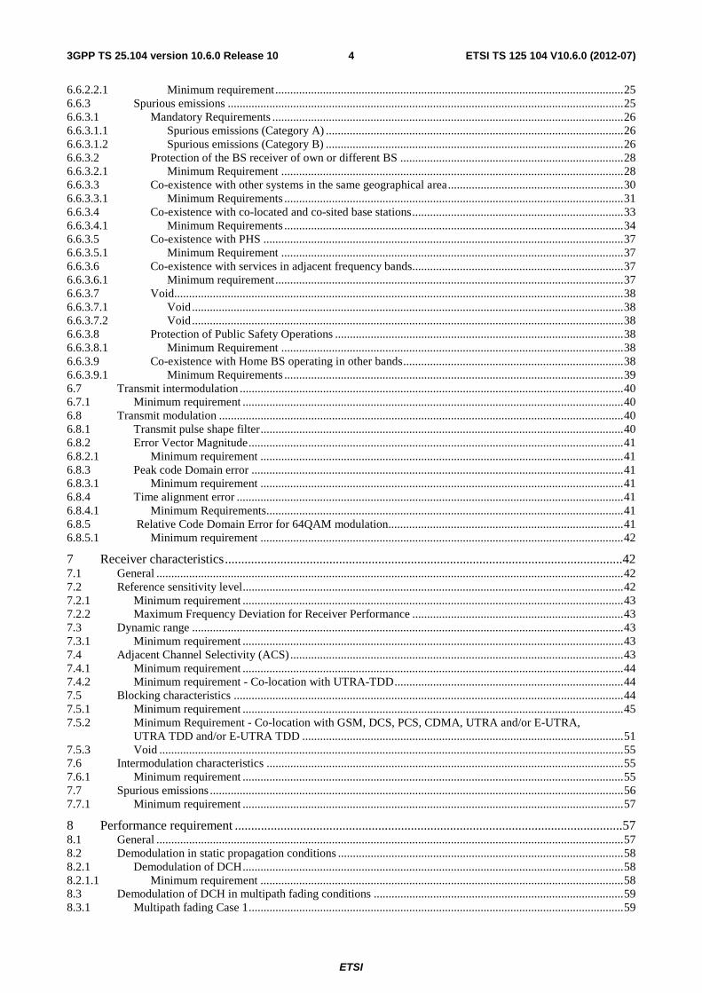
6.6.2.1 Spectrum emission mask
The mask defined in Tables 6.3 to 6.6 below may be mandatory in certain regions. In other regions this mask may not be applied.
For regions where this clause applies, the requirement shall be met by a base station transmitting on a single RF carrier configured in accordance with the manufacturer's specification. Emissions shall not exceed the maximum level specified in tables 6.3 to 6.6 for the appropriate BS maximum output power, in the frequency range from Δf = 2.5 MHz to Δfmax from the carrier frequency, where:
- Δf is the separation between the carrier frequency and the nominal -3dB point of the measuring filter closest to the carrier frequency.
- F_offset is the separation between the carrier frequency and the centre of the measuring filter.
- f_offsetmax is either 12.5 MHz or the offset to the UMTS Tx band edge as defined in section 5.2, whichever is the greater.
- Δfmax is equal to f_offsetmax minus half of the bandwidth of the measuring filter.
2.5 2.7 3.5
-15 0
Frequency separation Δf from the carrier [MHz]
Pow
er d
ensi
ty in
30k
Hz
[dB
m]
Δfmax
-20
-25
-30
-35
-40
Pow
er d
ensi
ty in
1 M
Hz
[dB
m]
-5
-10
-15
-20
-25
7.5
P = 39 dBmP = 39 dBm
P = 43 dBmP = 43 dBm
P = 31 dBmP = 31 dBm
Illustrative diagram of spectrum emission mask
Figure 6.2: Spectrum emission mask
Table 6.3: Spectrum emission mask values, BS maximum output power P ≥ 43 dBm
Frequency offset of measurement filter -3dB point,
Δf
Frequency offset of measurement
filter centre frequency, f_offset
Minimum requirement Measurement bandwidth
(Note 2)
2.5 MHz ≤ Δf < 2.7 MHz
2.515MHz ≤ f_offset < 2.715MHz
-14 dBm 30 kHz
2.7 MHz ≤ Δf < 3.5 MHz
2.715MHz ≤ f_offset < 3.515MHz dB
MHz
offsetfdBm ⎟
⎠
⎞⎜⎝
⎛ −⋅−− 715.2_
1514 30 kHz
(Note 1) 3.515MHz ≤ f_offset < 4.0MHz
-26 dBm 30 kHz
3.5 MHz ≤ Δf ≤ Δfmax
4.0MHz ≤ f_offset < f_offsetmax
-13 dBm 1 MHz

ETSI
ETSI TS 125 104 V10.6.0 (2012-07)233GPP TS 25.104 version 10.6.0 Release 10
Table 6.4: Spectrum emission mask values, BS maximum output power 39 ≤ P < 43 dBm
Frequency offset of measurement filter -3dB point,
Δf
Frequency offset of measurement filter centre frequency,
f_offset
Minimum requirement Measurement bandwidth
(Note 2)
2.5 MHz ≤ Δf < 2.7 MHz
2.515MHz ≤ f_offset < 2.715MHz
-14 dBm 30 kHz
2.7 MHz ≤ Δf < 3.5 MHz
2.715MHz ≤ f_offset < 3.515MHz dB
MHz
offsetfdBm ⎟
⎠
⎞⎜⎝
⎛ −⋅−− 715.2_
1514 30 kHz
(Note 1) 3.515MHz ≤ f_offset < 4.0MHz
-26 dBm 30 kHz
3.5 MHz ≤ Δf < 7.5 MHz
4.0MHz ≤ f_offset < 8.0MHz
-13 dBm 1 MHz
7.5 MHz ≤ Δf ≤ Δfmax
8.0MHz ≤ f_offset < f_offsetmax
P - 56 dB 1 MHz
Table 6.5: Spectrum emission mask values, BS maximum output power 31 ≤ P < 39 dBm
Frequency offset of measurement
filter -3dB point,Δf
Frequency offset of measurement filter centre frequency,
f_offset
Minimum requirement Measurement bandwidth
(Note 2)
2.5 MHz ≤ Δf < 2.7 MHz
2.515MHz ≤ f_offset < 2.715MHz
P - 53 dB 30 kHz
2.7 MHz ≤ Δf < 3.5 MHz
2.715MHz ≤ f_offset < 3.515MHz dB
MHz
offsetfdBP ⎟
⎠
⎞⎜⎝
⎛ −⋅−− 715.2_
1553 30 kHz
(Note 1) 3.515MHz ≤ f_offset < 4.0MHz
P - 65 dB 30 kHz
3.5 MHz ≤ Δf < 7.5 MHz
4.0MHz ≤ f_offset < 8.0MHz
P - 52 dB 1 MHz
7.5 MHz ≤ Δf ≤ Δfmax
8.0MHz ≤ f_offset < f_offsetmax
P - 56 dB 1 MHz
Table 6.6: Spectrum emission mask values, BS maximum output power P < 31 dBm
Frequency offset of measurement filter
-3dB point, Δf
Frequency offset of measurement filter centre
frequency, f_offset
Minimum requirement Measurement bandwidth
(Note 2) 2.5 MHz ≤ Δf < 2.7
MHz 2.515MHz ≤ f_offset <
2.715MHz -22 dBm 30 kHz
2.7 MHz ≤ Δf < 3.5 MHz
2.715MHz ≤ f_offset < 3.515MHz dB
MHz
offsetfdBm ⎟
⎠
⎞⎜⎝
⎛ −⋅−− 715.2_
1522 30 kHz
(Note 1) 3.515MHz ≤ f_offset < 4.0MHz
-34 dBm 30 kHz
3.5 MHz ≤ Δf < 7.5 MHz
4.0MHz ≤ f_offset < 8.0MHz -21 dBm 1 MHz
7.5 MHz ≤ Δf ≤ Δfmax 8.0MHz ≤ f_offset < f_offsetmax
-25 dBm 1 MHz
For operation in band II, IV, V, X, XII, XIII, XIV and XXV, the applicable additional requirements in Tables 6.6A, 6.6B or 6.6C apply in addition to the minimum requirements in Tables 6.3 to 6.6.

ETSI
ETSI TS 125 104 V10.6.0 (2012-07)243GPP TS 25.104 version 10.6.0 Release 10
Table 6.6A: Additional spectrum emission limits for Bands II, IV, X, XXV
Frequency offset of measurement filter -3dB point,
Δf
Frequency offset of measurement filter centre frequency,
f_offset
Additional requirement
Measurement bandwidth
(Note 2)
2.5 MHz ≤ Δf < 3.5 MHz
2.515MHz ≤ f_offset < 3.515MHz
-15 dBm 30 kHz
3.5 MHz ≤ Δf ≤ Δfmax
4.0MHz ≤ f_offset < f_offsetmax
-13 dBm 1 MHz
Table 6.6B: Additional spectrum emission limits for Band V
Frequency offset of measurement filter -3dB point,
Δf
Frequency offset of measurement filter centre frequency,
f_offset
Additional requirement
Measurement bandwidth
(Note 2)
2.5 MHz ≤ Δf < 3.5 MHz
2.515MHz ≤ f_offset < 3.515MHz
-15 dBm 30 kHz
3.5 MHz ≤ Δf ≤ Δfmax
3.55MHz ≤ f_offset < f_offsetmax
-13 dBm 100 kHz
Table 6.6C: Additional spectrum emission limits for Bands XII, XIII, XIV
Frequency offset of measurement filter -3dB point,
Δf
Frequency offset of measurement filter centre frequency,
f_offset
Additional requirement
Measurement bandwidth
(Note 2)
2.5 MHz ≤ Δf < 2.6 MHz
2.515MHz ≤ f_offset < 2.615MHz
-13 dBm 30 kHz
2.6 MHz ≤ Δf ≤ Δfmax
2.65MHz ≤ f_offset < f_offsetmax
-13 dBm 100 kHz
For Home BS, the applicable additional requirements in Tables 6.6D or 6.6E apply in addition to the minimum requirements in Tables 6.3 to 6.6.
Table 6.6D: Additional spectrum emission limit for Home BS, BS maximum output power 6 ≤ P ≤ 20 dBm
Frequency offset of measurement filter -3dB point,
Δf
Frequency offset of measurement filter centre frequency,
f_offset
Additional requirement
Measurement bandwidth
(Note 2)
12.5 MHz ≤ Δf ≤ Δfmax
13MHz ≤ f_offset < f_offsetmax
P - 56 dBm 1 MHz
Table 6.6E: Additional spectrum emission limit for Home BS, BS maximum output power P < 6 dBm
Frequency offset of measurement filter -3dB point,
Δf
Frequency offset of measurement filter centre frequency,
f_offset
Additional requirement
Measurement bandwidth
(Note 2)
12.5 MHz ≤ Δf ≤ Δfmax
13MHz ≤ f_offset < f_offsetmax
-50 dBm 1 MHz
In certain regions the following requirement may apply for protection of DTT. For UTRA BS operating in Band XX, the level of emissions in the band 470-790 MHz, measured in an 8MHz filter bandwidth on centre frequencies Ffilter according to Table 6.6F, shall not exceed the maximum emission level PEM,N declared by the manufacturer.

ETSI
ETSI TS 125 104 V10.6.0 (2012-07)253GPP TS 25.104 version 10.6.0 Release 10
Table 6.6F: Declared emissions levels for protection of DTT
Filter centre frequency, Ffilter
Measurement bandwidth
Declared emission level [dBm]
Ffilter = 8*N + 306 (MHz); 21 ≤ N ≤ 60
8 MHz PEM,N
NOTE: The regional requirement is defined in terms of EIRP (effective isotropic radiated power), which is dependent on both the BS emissions at the antenna connector and the deployment (including antenna gain and feeder loss). The requirement defined above provides the characteristics of the basestation needed to verify compliance with the regional requirement. Compliance with the regional requirement can be determined using the method outlined in Annex D.
Notes for Tables 6.3, 6.4, 6.5 & 6.6
NOTE 1: This frequency range ensures that the range of values of f_offset is continuous.
NOTE 2 As a general rule, the resolution bandwidth of the measuring equipment should be equal to the measurement bandwidth. However, to improve measurement accuracy, sensitivity and efficiency, the resolution bandwidth can be smaller than the measurement bandwidth. When the resolution bandwidth is smaller than the measurement bandwidth, the result should be integrated over the measurement bandwidth in order to obtain the equivalent noise bandwidth of the measurement bandwidth.
6.6.2.2 Adjacent Channel Leakage power Ratio (ACLR)
Adjacent Channel Leakage power Ratio (ACLR) is the ratio of the RRC filtered mean power centered on the assigned channel frequency to the RRC filtered mean power centered on an adjacent channel frequency.
The requirements shall apply whatever the type of transmitter considered (single carrier or multi-carrier). It applies for all transmission modes foreseen by the manufacturer's specification.
6.6.2.2.1 Minimum requirement
The ACLR shall be higher than the value specified in Table 6.7.
Table 6.7: BS ACLR
BS adjacent channel offset below the first or above the last carrier frequency used
ACLR limit
5 MHz 45 dB 10 MHz 50 dB
Note 1: In certain regions, the adjacent channel power (the RRC filtered mean power centered on an adjacent channel frequency) shall be less than or equal to -8.0 dBm/3.84 MHz (for Band I, IX, XI and XXI) or
+2.0dBm/3.84MHz (for Band VI, VIII and XIX) or as specified by the ACLR limit, whichever is the higher. This note is not applicable for Home BS.
Note 2: For Home BS, the adjacent channel power (the RRC filtered mean power centered on an adjacent channel frequency) shall be less than or equal to -44.2 dBm/3.84MHz or as specified by the ACLR limit, whichever is the higher.
6.6.3 Spurious emissions
Spurious emissions are emissions which are caused by unwanted transmitter effects such as harmonics emission, parasitic emission, intermodulation products and frequency conversion products, but exclude out of band emissions. This is measured at the base station antenna connector.
The requirements shall apply whatever the type of transmitter considered (single carrier or multiple-carrier). It applies for all transmission modes foreseen by the manufacturer's specification.

ETSI
ETSI TS 125 104 V10.6.0 (2012-07)263GPP TS 25.104 version 10.6.0 Release 10
The requirements (except 6.6.3.5 and 6.6.3.8 and specifically stated exceptions in Table 6.11) apply at frequencies within the specified frequency ranges, which are more than 12.5MHz below the first carrier frequency used or more than 12.5MHz above the last carrier frequency used.
Unless otherwise stated, all requirements are measured as mean power (RMS).
6.6.3.1 Mandatory Requirements
The requirements of either subclause 6.6.3.1.1 or subclause 6.6.3.1.2 shall apply.
6.6.3.1.1 Spurious emissions (Category A)
The following requirements shall be met in cases where Category A limits for spurious emissions, as defined in ITU-R Recommendation SM.329 [1], are applied.
6.6.3.1.1.1 Minimum Requirement
The power of any spurious emission shall not exceed:
Table 6.8: BS Mandatory spurious emissions limits, Category A
Band Maximum level Measurement Bandwidth
Note
9kHz - 150kHz
-13 dBm
1 kHz Note 1 150kHz - 30MHz 10 kHz Note 1 30MHz - 1GHz 100 kHz Note 1
1GHz - 12.75 GHz 1 MHz Note 2 12.75 GHz - 5th harmonic
of the upper frequency edge of the DL operating
band in GHz
1 MHz Note 2, Note 3
NOTE 1: Bandwidth as in ITU-R SM.329 [1], s4.1 NOTE 2: Upper frequency as in ITU-R SM.329 [1], s2.5 table 1 NOTE 3: Applies only for Band XXII
6.6.3.1.2 Spurious emissions (Category B)
The following requirements shall be met in cases where Category B limits for spurious emissions, as defined in ITU-R Recommendation SM.329 [1], are applied.

ETSI
ETSI TS 125 104 V10.6.0 (2012-07)273GPP TS 25.104 version 10.6.0 Release 10
6.6.3.1.2.1 Minimum Requirement
The power of any spurious emission shall not exceed:
Table 6.9: BS Mandatory spurious emissions limits, operating band I, II, III, IV, VII, X, XXII, XXV (Category B)
Band Maximum Level
Measurement Bandwidth
Note
9 kHz ↔ 150 kHz -36 dBm 1 kHz Note 1 150 kHz ↔ 30 MHz -36 dBm 10 kHz Note 1 30 MHz ↔ 1 GHz -36 dBm 100 kHz Note 1
1 GHz ↔ Flow - 10 MHz -30 dBm 1 MHz Note 1 Flow - 10 MHz ↔ Fhigh + 10 MHz -15 dBm 1 MHz Note 2
Fhigh + 10 MHz ↔ 12.75 GHz -30 dBm 1 MHz Note 3 12.75 GHz - 5th harmonic of the upper frequency edge of the DL
operating band in GHz
-30 dBm 1 MHz Note 3, Note 4
NOTE 1: Bandwidth as in ITU-R Recommendation SM.329 [1], s4.1 NOTE 2: Limit based on ITU-R Recommendation SM.329 [1], s4.3 and Annex 7 NOTE 3: Bandwidth as in ITU-R Recommendation SM.329 [1], s4.1. Upper frequency as in ITU-R
SM.329 [1], s2.5 table 1 NOTE 4: Applies only for Band XXII Key: Flow: The lowest downlink frequency of the operating band as defined in Table 5.0. Fhigh: The highest downlink frequency of the operating band as defined in Table 5.0.
Table 6.9A: BS Mandatory spurious emissions limits, operating band V, VIII, XII, XIII, XIV, XX (Category B)
Band Maximum Level
Measurement Bandwidth
Note
9 kHz ↔ 150 kHz -36 dBm 1 kHz Note 1 150 kHz ↔ 30 MHz -36 dBm 10 kHz Note 1
30 MHz ↔ Flow - 10 MHz -36 dBm 100 kHz Note 1 Flow - 10 MHz ↔ Fhigh + 10 MHz -16 dBm 100 kHz Note 2
Fhigh + 10 MHz ↔ 1 GHz -36 dBm 100 kHz Note 1 1GHz ↔ 12.75GHz -30 dBm 1 MHz Note 3
NOTE 1: Bandwidth as in ITU-R Recommendation SM.329 [1], s4.1 NOTE 2: Limit based on ITU-R Recommendation SM.329 [1], s4.3 and Annex 7 NOTE 3: Bandwidth as in ITU-R Recommendation SM.329 [1], s4.1. Upper frequency as in ITU-R
SM.329 [1], s2.5 table 1 Key: Flow: The lowest downlink frequency of the operating band as defined in Table 5.0. Fhigh: The highest downlink frequency of the operating band as defined in Table 5.0.

ETSI
ETSI TS 125 104 V10.6.0 (2012-07)283GPP TS 25.104 version 10.6.0 Release 10
Table 6.9B: (void)
Table 6.9C: (void)
Table 6.9D: (void)
Table 6.9E: (void)
Table 6.9F: (void)
Table 6.9G: (void)
6.6.3.2 Protection of the BS receiver of own or different BS
This requirement shall be applied in order to prevent the receivers of the BSs being desensitised by emissions from a BS transmitter. This is measured at the transmit antenna port for any type of BS which has common or separate Tx/Rx antenna ports.
6.6.3.2.1 Minimum Requirement
The power of any spurious emission shall not exceed:
Table 6.10: Wide Area BS Spurious emissions limits for protection of the BS receiver
Operating Band
Band Maximum Level
Measurement Bandwidth
Note
I 1920 - 1980MHz -96 dBm 100 kHz II 1850-1910 MHz -96 dBm 100 kHz III 1710-1785 MHz -96 dBm 100 kHz IV 1710-1755 MHz -96 dBm 100 kHz V 824-849 MHz -96 dBm 100 kHz
VI, XIX 815-850 MHz -96 dBm 100 kHz VII 2500-2570 MHz -96 dBm 100 kHz VIII 880-915 MHz -96 dBm 100 kHz IX 1749.9-1784.9 MHz -96 dBm 100 kHz X 1710-1770 MHz -96 dBm 100 kHz XI 1427.9 - 1447.9 MHz -96 dBm 100 kHz XII 699 - 716 MHz -96 dBm 100 kHz XIII 777 - 787 MHz -96 dBm 100 kHz XIV 788 - 798 MHz -96 dBm 100 kHz XX 832 - 862 MHz -96 dBm 100 kHz XXI 1447.9 - 1462.9 MHz -96 dBm 100 kHz XXII 3410 - 3490 MHz -96 dBm 100 kHz XXV 1850-1915 MHz -96 dBm 100 kHz

ETSI
ETSI TS 125 104 V10.6.0 (2012-07)293GPP TS 25.104 version 10.6.0 Release 10
Table 6.10A: Medium Range BS Spurious emissions limits for protection of the BS receiver
Operating Band
Band Maximum Level
Measurement Bandwidth
Note
I 1920 - 1980MHz -86 dBm 100 kHz II 1850-1910 MHz -86 dBm 100 kHz III 1710-1785 MHz -86 dBm 100 kHz IV 1710-1755 MHz -86 dBm 100 kHz V 824-849 MHz -86 dBm 100 kHz
VI, XIX 815-850 MHz -86 dBm 100 kHz VII 2500-2570 MHz -86 dBm 100 kHz VIII 880-915 MHz -86 dBm 100 kHz IX 1749.9-1784.9 MHz -86 dBm 100 kHz X 1710-1770 MHz -86 dBm 100 kHz XI 1427.9 - 1447.9 MHz -86 dBm 100 kHz XII 699 - 716 MHz -86 dBm 100 kHz XIII 777 - 787 MHz -86 dBm 100 kHz XIV 788 - 798 MHz -86 dBm 100 kHz XX 832 - 862 MHz -86 dBm 100 kHz XXI 1447.9 - 1462.9 MHz -86 dBm 100 kHz XXII 3410 - 3490 MHz -86 dBm 100 kHz XXV 1850-1915 MHz -86 dBm 100 kHz
Table 6.10B: Local Area BS Spurious emissions limits for protection of the BS receiver
Operating Band
Band Maximum Level
Measurement Bandwidth
Note
I 1920 - 1980MHz -82 dBm 100 kHz II 1850-1910 MHz -82 dBm 100 kHz III 1710-1785 MHz -82 dBm 100 kHz IV 1710-1755 MHz -82 dBm 100 kHz V 824-849 MHz -82 dBm 100 kHz
VI, XIX 815-850 MHz -82 dBm 100 kHz VII 2500-2570 MHz -82 dBm 100 kHz VIII 880-915 MHz -82 dBm 100 kHz IX 1749.9-1784.9 MHz -82 dBm 100 kHz X 1710-1770 MHz -82 dBm 100 kHz XI 1427.9 - 1447.9 MHz -82 dBm 100 kHz XII 699 - 716 MHz -82 dBm 100 kHz XIII 777 - 787 MHz -82 dBm 100 kHz XIV 788 - 798 MHz -82 dBm 100 kHz XX 832 - 862 MHz -82 dBm 100 kHz XXI 1447.9 - 1462.9 MHz -82 dBm 100 kHz XXII 3410 - 3490 MHz -82 dBm 100 kHz XXV 1850-1915 MHz -82 dBm 100 kHz

ETSI
ETSI TS 125 104 V10.6.0 (2012-07)303GPP TS 25.104 version 10.6.0 Release 10
Table 6.10C: Home BS Spurious emissions limits for protection of the BS receiver
Operating Band
Band Maximum Level
Measurement Bandwidth
Note
I 1920 - 1980MHz -82 dBm 100 kHz II 1850-1910 MHz -82 dBm 100 kHz III 1710-1785 MHz -82 dBm 100 kHz IV 1710-1755 MHz -82 dBm 100 kHz V 824-849 MHz -82 dBm 100 kHz
VI, XIX 815-850 MHz -82 dBm 100 kHz VII 2500-2570 MHz -82 dBm 100 kHz VIII 880-915 MHz -82 dBm 100 kHz IX 1749.9-1784.9 MHz -82 dBm 100 kHz X 1710-1770 MHz -82 dBm 100 kHz XI 1427.9 - 1447.9 MHz -82 dBm 100 kHz XII 699 - 716 MHz -82 dBm 100 kHz XIII 777 - 787 MHz -82 dBm 100 kHz XIV 788 - 798 MHz -82 dBm 100 kHz XX 832 - 862 MHz -82 dBm 100 kHz XXI 1447.9 - 1462.9 MHz -82 dBm 100 kHz XXII 3410 - 3490 MHz -82 dBm 100 kHz XXV 1850-1915 MHz -82 dBm 100 kHz
6.6.3.3 Co-existence with other systems in the same geographical area
These requirements may be applied for the protection of UE, MS and/or BS operating in other frequency bands in the same geographical area. The requirements may apply in geographic areas in which both a UTRA FDD BS and a system operating in another frequency band than the FDD operating band are deployed. The system operating in the other frequency band may be GSM, DCS, PCS, CDMA, E-UTRA and/or UTRA.

ETSI
ETSI TS 125 104 V10.6.0 (2012-07)313GPP TS 25.104 version 10.6.0 Release 10
6.6.3.3.1 Minimum Requirements
The power of any spurious emission shall not exceed the limits of Table 6.11 for a BS where requirements for co-existence with the system listed in the first column apply.
Table 6.11: BS Spurious emissions limits for UTRA FDD BS in geographic coverage area of systems operating in other frequency bands
System type operating in
the same geographical
area
Band for co-existence
requirement
Maximum Level
Measurement Bandwidth
Note
GSM900 921 - 960 MHz -57 dBm 100 kHz This requirement does not apply to UTRA FDD operating in band VIII
876 - 915 MHz -61 dBm 100 kHz For the frequency range 880-915 MHz, this requirement does not apply to UTRA FDD operating in band VIII, since it is already covered by the requirement in sub-clause 6.6.3.2.
DCS1800 1805 - 1880 MHz -47 dBm 100 kHz This requirement does not apply to UTRA FDD operating in band III
1710 - 1785 MHz -61 dBm 100 kHz This requirement does not apply to UTRA FDD operating in band III, since it is already covered by the requirement in sub-clause 6.6.3.2.
PCS1900 1930 - 1990 MHz -47 dBm 100 kHz This requirement does not apply to UTRA FDD BS operating in frequency band II or band XXV
1850 - 1910 MHz -61 dBm 100 kHz This requirement does not apply to UTRA FDD BS operating in frequency band II or band XXV, since it is already covered by the requirement in sub-clause 6.6.3.2.
GSM850 or CDMA850
869 - 894 MHz -57 dBm 100 kHz This requirement does not apply to UTRA FDD BS operating in frequency band V
824 - 849 MHz -61 dBm 100 kHz This requirement does not apply to UTRA FDD BS operating in frequency band V, since it is already covered by the requirement in sub-clause 6.6.3.2.
UTRA FDD Band I or E-UTRA Band 1
2110 - 2170 MHz -52 dBm 1 MHz This requirement does not apply to UTRA FDD BS operating in band I,
1920 - 1980 MHz -49 dBm 1 MHz This requirement does not apply to UTRA FDD BS operating in band I, since it is already covered by the requirement in sub-clause 6.6.3.2.
UTRA FDD Band II or E-UTRA Band 2
1930 - 1990 MHz -52 dBm 1 MHz This requirement does not apply to UTRA FDD BS operating in band II or band XXV
1850 - 1910 MHz -49 dBm 1 MHz This requirement does not apply to UTRA FDD BS operating in band II or band XXV, since it is already covered by the requirement in sub-clause 6.6.3.2.
UTRA FDD Band III or E-UTRA Band 3
1805 - 1880 MHz -52 dBm 1 MHz This requirement does not apply to UTRA FDD BS operating in band III or band IX
1710 - 1785 MHz -49 dBm 1 MHz This requirement does not apply to UTRA FDD BS operating in band III, since it is already covered by the requirement in sub-clause 6.6.3.2. For UTRA BS operating in band IX, it applies for 1710 MHz to 1749.9 MHz and 1784.9 MHz to 1785 MHz, while the rest is covered in sub-clause 6.6.3.2.
UTRA FDD Band IV or E-UTRA Band 4
2110 - 2155 MHz -52 dBm 1 MHz This requirement does not apply to UTRA FDD BS operating in band IV or band X
1710 - 1755 MHz -49 dBm 1 MHz This requirement does not apply to UTRA FDD BS operating in band IV or band X, since it is already covered by the requirement in sub-clause 6.6.3.2.
UTRA FDD Band V or E-UTRA Band 5
869 - 894 MHz -52 dBm 1 MHz This requirement does not apply to UTRA FDD BS operating in band V
824 - 849 MHz -49 dBm 1 MHz This requirement does not apply to UTRA FDD BS operating in band V, since it is already covered by the requirement in sub-clause 6.6.3.2.
UTRA FDD Band VI or XIX,
860 - 895 MHz -52 dBm 1 MHz This requirement does not apply to UTRA FDD BS operating in band VI or XIX

ETSI
ETSI TS 125 104 V10.6.0 (2012-07)323GPP TS 25.104 version 10.6.0 Release 10
E-UTRA Band 6, 18 or 19
815 - 850 MHz -49 dBm 1 MHz This requirement does not apply to UTRA FDD BS operating in band VI or XIX, since it is already covered by the requirement in sub-clause 6.6.3.2.
UTRA FDD Band VII or
E-UTRA Band 7
2620 - 2690 MHz -52 dBm 1 MHz This requirement does not apply to UTRA FDD BS operating in band VII,
2500 - 2570 MHz -49 dBm 1 MHz This requirement does not apply to UTRA FDD BS operating in band VII, since it is already covered by the requirement in sub-clause 6.6.3.2.
UTRA FDD Band VIII or
E-UTRA Band 8
925 - 960 MHz -52 dBm 1 MHz This requirement does not apply to UTRA FDD BS operating in band VIII.
880 - 915 MHz -49 dBm 1 MHz This requirement does not apply to UTRA FDD BS operating in band VIII, since it is already covered by the requirement in sub-clause 6.6.3.2.
UTRA FDD Band IX or E-UTRA Band 9
1844.9 - 1879.9 MHz
-52 dBm 1 MHz This requirement does not apply to UTRA FDD BS operating in band IX
1749.9 - 1784.9 MHz
-49 dBm 1 MHz This requirement does not apply to UTRA FDD BS operating in band IX, since it is already covered by the requirement in sub-clause 6.6.3.2.
UTRA FDD Band X or E-UTRA Band 10
2110 - 2170 MHz -52 dBm 1 MHz This requirement does not apply to UTRA FDD BS operating in band IV or band X.
1710 - 1770 MHz -49 dBm 1 MHz This requirement does not apply to UTRA FDD BS operating in band X, since it is already covered by the requirement in sub-clause 6.6.3.2. For UTRA FDD BS operating in Band IV, it applies for 1755 MHz to 1770 MHz, while the rest is covered in sub-clause 6.6.3.2.
UTRA FDD Band XI or XXI
or E-UTRA
Band 11 or 21
1475.9 - 1510.9 MHz
-52 dBm 1 MHz This requirement does not apply to UTRA FDD BS operating in band XI or XXI.
1427.9 - 1447.9 MHz
-49 dBm 1 MHz This requirement does not apply to UTRA FDD BS operating in band XI, since it is already covered by the requirement in sub-clause 6.6.3.2.
1447.9 - 1462.9 MHz
-49 dBm 1 MHz This requirement does not apply to UTRA FDD BS operating in band XXI, since it is already covered by the requirement in sub-clause 6.6.3.2.
UTRA FDD Band XII or
E-UTRA Band 12
729 - 746 MHz -52 dBm 1 MHz This requirement does not apply to UTRA FDD BS operating in band XII
699 - 716 MHz -49 dBm 1 MHz This requirement does not apply to UTRA FDD BS operating in band XII, since it is already covered by the requirement in sub-clause 6.6.3.2.
UTRA FDD Band XIII or
E-UTRA Band 13
746 - 756 MHz -52 dBm 1 MHz This requirement does not apply to UTRA FDD BS operating in band XIII
777 - 787 MHz -49 dBm 1 MHz This requirement does not apply to UTRA FDD BS operating in band XIII, since it is already covered by the requirement in sub-clause 6.6.3.2.
UTRA FDD Band XIV or
E-UTRA Band 14
758 - 768 MHz -52 dBm 1 MHz This requirement does not apply to UTRA FDD BS operating in band XIV
788 - 798 MHz -49 dBm 1 MHz This requirement does not apply to UTRA FDD BS operating in band XIV, since it is already covered by the requirement in sub-clause 6.6.3.2.
E-UTRA Band 17
734 - 746 MHz -52 dBm 1 MHz This requirement does not apply to UTRA FDD BS operating in band XII
704 - 716 MHz -49 dBm 1 MHz This requirement does not apply to UTRA FDD BS operating in band XII, since it is already covered by the requirement in sub-clause 6.6.3.2.
UTRA FDD Band XX or
E-UTRA Band 20
791 - 821 MHz -52 dBm 1 MHz This requirement does not apply to UTRA FDD BS operating in band XX
832 - 862 MHz -49 dBm 1 MHz This requirement does not apply to UTRA FDD BS operating in band XX, since it is already covered by the requirement in sub-clause 6.6.3.2.
UTRA FDD Band XXII or
E-UTRA Band 22
3510 -3590 MHz -52 1 MHz This requirement does not apply to UTRA FDD BS operating in band XXII.
3410 -3490 MHz -49 1 MHz This requirement does not apply to UTRA FDD BS operating in band XXII, since it is already covered by the requirement in sub-clause 6.6.3.2.
E-UTRA Band 23
2180 - 2200 MHz -52 dBm 1 MHz 2000 - 2020 MHz -49 dBm 1 MHz This requirement does not apply to UTRA FDD BS
operating in Band II or XXV, where the limits are defined separately.
2000 – 2010 MHz -30 dBm 1 MHz This requirement only applies to UTRA FDD BS

ETSI
ETSI TS 125 104 V10.6.0 (2012-07)333GPP TS 25.104 version 10.6.0 Release 10
2010 – 2020 MHZ -49 dBm 1 MHz operating in Band II or Band XXV. This requirement applies starting 5 MHz above the Band XXV downlink operating band. (Note 3)
E-UTRA Band 24
1525 – 1559 MHz -52 dBm 1 MHz 1626.5 – 1660.5
MHz -49 dBm 1 MHz
UTRA FDD Band XXV or
E-UTRA Band 25
1930 - 1995 MHz -52 dBm 1 MHz This requirement does not apply to UTRA FDD BS operating in band II or band XXV
1850 - 1915 MHz -49 dBm 1 MHz This requirement does not apply to UTRA FDD BS operating in band XXV, since it is already covered by the requirement in sub-clause 6.6.3.2. For UTRA FDD BS operating in Band II, it applies for 1910 MHz to 1915 MHz, while the rest is covered in sub-clause 6.6.3.2.
UTRA TDD Band a) or E-
UTRA Band 33
1900 – 1920 MHz -52 dBm 1 MHz
UTRA TDD Band a) or E-
UTRA Band 34
2010 – 2025 MHz -52 dBm 1 MHz
UTRA TDD Band d) or E-
UTRA Band 38
2570 – 2620 MHz -52 dBm 1 MHz
UTRA TDD Band f) or E-
UTRA Band 39
1880 – 1920 MHz -52 dBm 1 MHz Applicable in China
UTRA TDD in Band e) or E-
UTRA Band 40
2300 – 2400 MHz -52 dBm 1 MHz
E-UTRA Band 41
2496 - 2690 MHz -52 dBm 1 MHz
E-UTRA Band 42
3400 – 3600 MHz -52 dBm 1 MHz
E-UTRA Band 43
3600 – 3800 MHz -52 dBm 1 MHz
NOTE 1: The co-existence requirements do not apply for the 10 MHz frequency range immediately outside the downlink operating band (see Table 5.0). Emission limits for this excluded frequency range may be covered by local or regional requirements.
NOTE 2: The table above assumes that two operating bands, where the frequency ranges would be overlapping, are not deployed in the same geographical area. For such a case of operation with overlapping frequency arrangements in the same geographical area, special co-existence requirements may apply that are not covered by the 3GPP specifications.
NOTE 3: This requirement does not apply to a Band II UTRA BS of an earlier release. In addition, it does not apply to an UTRA Band II BS from an earlier release manufactured before 31 December, 2012, which is upgraded to support Rel-10 features, where the upgrade does not affect existing RF parts of the radio unit related to this requirement.
6.6.3.4 Co-existence with co-located and co-sited base stations
These requirements may be applied for the protection of other BS receivers when GSM, DCS, PCS, CDMA, E-UTRA and/or UTRA BS are co-located with a UTRA FDD BS.
The requirements in this chapter assume a 30 dB coupling loss between transmitter and receiver. If BSs of different classes are co-sited, the coupling loss should be increased by the value as stated in TR 25.942 [4] chapter 10.3 in Table 10.1 and Table 10.2.

ETSI
ETSI TS 125 104 V10.6.0 (2012-07)343GPP TS 25.104 version 10.6.0 Release 10
6.6.3.4.1 Minimum Requirements
The power of any spurious emission shall not exceed the limits of Table 6.12 for a Wide Area (WA) BS where requirements for co-location with a BS type listed in the first column apply.
Table 6.12: BS Spurious emissions limits for Wide Area BS co-located with another BS
Type of co-located BS Band for co-location requirement
Maximum Level
Measurement Bandwidth
Note
Macro GSM900 876 – 915 MHz -98 dBm 100 kHz Macro DCS1800 1710 – 1785 MHz -98 dBm 100 kHz Macro PCS1900 1850 – 1910 MHz -98 dBm 100 kHz
Macro GSM850 or CDMA850
824 – 849 MHz -98 dBm 100 kHz
WA UTRA FDD Band I or E-UTRA Band 1
1920 – 1980 MHz -96 dBm 100 kHz
WA UTRA FDD Band II or E-UTRA Band 2
1850 – 1910 MHz -96 dBm 100 kHz
WA UTRA FDD Band III or E-UTRA Band 3
1710 – 1785 MHz -96 dBm 100 kHz
WA UTRA FDD Band IV or E-UTRA Band 4
1710 – 1755 MHz -96 dBm 100 kHz
WA UTRA FDD Band V or E-UTRA Band 5
824 – 849 MHz -96 dBm 100 kHz
WA UTRA FDD Band VI or XIX, or E-UTRA Band 6, 18 or 19
815 – 850 MHz -96 dBm 100 kHz
WA UTRA FDD Band VII or E-UTRA Band 7
2500 – 2570 MHz -96 dBm 100 KHz
WA UTRA FDD Band VIII or E-UTRA Band 8
880 – 915 MHz -96 dBm 100 KHz
WA UTRA FDD Band IX or E-UTRA Band 9
1749.9 – 1784.9 MHz -96 dBm 100 KHz
WA UTRA FDD Band X or E-UTRA Band 10
1710 – 1770 MHz -96 dBm 100 kHz
WA UTRA FDD Band XI or E-UTRA Band 11
1427.9 – 1447.9 MHz -96 dBm 100 kHz
WA UTRA FDD Band XII or E-UTRA Band 12
699 – 716 MHz -96 dBm 100 KHz
WA UTRA FDD Band XIII or E-UTRA Band 13
777 – 787 MHz -96 dBm 100 kHz
WA UTRA FDD Band XIV or E-UTRA Band 14
788 – 798 MHz -96 dBm 100 kHz
WA E-UTRA Band 17 704 – 716 MHz -96 dBm 100 KHz WA UTRA FDD Band XX
or E-UTRA Band 20 832 – 862 MHz -96 dBm 100 KHz
WA UTRA FDD Band XXI or E-UTRA Band 21
1447.9 – 1462.9 MHz -96 dBm 100 kHz
WA UTRA FDD Band XXII or E-UTRA Band 22
3410 – 3490 MHz -96 dBm 100 kHz
WA E-UTRA Band 23 2000 - 2020 MHz -96 dBm 100 kHz WA E-UTRA Band 24 1626.5 – 1660.5 MHz -96 dBm 100 kHz WA UTRA FDD Band
XXV or E-UTRA Band 25 1850 - 1915 MHz -96 dBm 100 kHz
WA UTRA TDD Band a) or E-UTRA Band 33
1900 – 1920 MHz -86 dBm 1 MHz
WA UTRA TDD Band a) or E-UTRA Band 34
2010 – 2025 MHz -86 dBm 1 MHz
WA UTRA TDD Band d) or E-UTRA Band 38
2570 – 2620 MHz -86 dBm 1 MHz
WA UTRA TDD Band f) or E-UTRA Band 39
1880 – 1920MHz -86 dBm 1 MHz Applicable in China
WA UTRA TDD Band e) or E-UTRA Band 40
2300 – 2400MHz -86 dBm 1 MHz
E-UTRA Band 41 2496 – 2690 MHz -86 dBm 1 MHz WA E-UTRA Band 42 3400 – 3600 MHz -86 dBm 1 MHz

ETSI
ETSI TS 125 104 V10.6.0 (2012-07)353GPP TS 25.104 version 10.6.0 Release 10
WA E-UTRA Band 43 3600 – 3800 MHz -86 dBm 1 MHz NOTE 1: The co-location requirements do not apply for the 10 MHz frequency range immediately outside the
BS transmit frequency range of a downlink operating band (see Table 5.0). The current state-of-the-art technology does not allow a single generic solution for co-location with other system on adjacent frequencies for 30dB BS-BS minimum coupling loss. However, there are certain site-engineering solutions that can be used. These techniques are addressed in TR 25.942 [4].
NOTE 2: The table above assumes that two operating bands, where the frequency ranges would be overlapping, are not deployed in the same geographical area. For such a case of operation with overlapping frequency arrangements in the same geographical area, special co-existence requirements may apply that are not covered by the 3GPP specifications.
The power of any spurious emission shall not exceed the limits of Table 6.13 for a Medium Range (MR) BS where requirements for co-location with a BS type listed in the first column apply.
Table 6.13: BS Spurious emissions limits for Medium Range BS co-located with another BS
Type of co-located BS Band for co-location requirement
Maximum Level
Measurement Bandwidth
Note
Micro GSM900 876-915 MHz -91 dBm 100 kHz Micro DCS1800 1710 - 1785 MHz -96 dBm 100 kHz Micro PCS1900 1850 - 1910 MHz -96 dBm 100 kHz Micro GSM850 824 - 849 MHz -91 dBm 100 kHz
MR UTRA FDD Band I 1920 - 1980 MHz -86 dBm 100 kHz MR UTRA FDD Band II 1850 - 1910 MHz -86 dBm 100 kHz MR UTRA FDD Band III 1710 - 1785 MHz -86 dBm 100 kHz MR UTRA FDD Band IV 1710 - 1755 MHz -86 dBm 100 kHz MR UTRA FDD Band V 824 - 849 MHz -86 dBm 100 kHz MR UTRA FDD Band VI
or XIX 815 - 850 MHz -86 dBm 100 kHz
MR UTRA FDD Band VII 2500 - 2570 MHz -86 dBm 100 KHz MR UTRA FDD Band VIII 880 - 915 MHz -86 dBm 100 KHz MR UTRA FDD Band IX 1749.9 - 1784.9 MHz -86 dBm 100 KHz MR UTRA FDD Band X 1710 - 1770 MHz -86 dBm 100 kHz MR UTRA FDD Band XI 1427.9 - 1447.9 MHz -86 dBm 100 kHz MR UTRA FDD Band XII 699 - 716 MHz -86 dBm 100 KHz MR UTRA FDD Band XIII 777 - 787 MHz -86 dBm 100 kHz MR UTRA FDD Band XIV 788 - 798 MHz -86 dBm 100 kHz MR UTRA FDD Band XX 832 - 862 MHz -86 dBm 100 kHz MR UTRA FDD Band XXI 1447.9 - 1462.9 MHz -86 dBm 100 kHz
MR UTRA FDD Band XXII
3410 – 3490 MHz -86 dBm 100 kHz
MR UTRA FDD Band XXV
1850 - 1915 MHz -86 dBm 100 kHz
NOTE 1: The co-location requirements do not apply for the 10 MHz frequency range immediately outside the BS transmit frequency range of a downlink operating band (see Table 5.0). The current state-of-the-art technology does not allow a single generic solution for co-location with other system on adjacent frequencies for 30dB BS-BS minimum coupling loss. However, there are certain site-engineering solutions that can be used. These techniques are addressed in TR 25.942 [4].
NOTE 2: The table above assumes that two operating bands, where the frequency ranges would be overlapping, are not deployed in the same geographical area. For such a case of operation with overlapping frequency arrangements in the same geographical area, special co-existence requirements may apply that are not covered by the 3GPP specifications.

ETSI
ETSI TS 125 104 V10.6.0 (2012-07)363GPP TS 25.104 version 10.6.0 Release 10
The power of any spurious emission shall not exceed the limits of Table 6.14 for a Local Area (LA) BS where requirements for co-location with a BS type listed in the first column apply.
Table 6.14: BS Spurious emissions limits for Local Area BS co-located with another BS
Type of co-located BS Band for co-location requirement
Maximum Level
Measurement Bandwidth
Note
Pico GSM900 876-915 MHz -70 dBm 100 kHz Pico DCS1800 1710 - 1785 MHz -80 dBm 100 kHz Pico PCS1900 1850 - 1910 MHz -80 dBm 100 kHz Pico GSM850 824 - 849 MHz -70 dBm 100 kHz
LA UTRA FDD Band I or E-UTRA Band 1
1920 - 1980 MHz -82 dBm 100 kHz
LA UTRA FDD Band II or E-UTRA Band 2
1850 - 1910 MHz -82 dBm 100 kHz
LA UTRA FDD Band III or E-UTRA Band 3
1710 - 1785 MHz -82 dBm 100 kHz
LA UTRA FDD Band IV or E-UTRA Band 4
1710 - 1755 MHz -82 dBm 100 kHz
LA UTRA FDD Band V or E-UTRA Band 5
824 - 849 MHz -82 dBm 100 kHz
LA UTRA FDD Band VI or XIX or E-UTRA Band 6, 18 or 19
815 - 850 MHz -82 dBm 100 kHz
LA UTRA FDD Band VII or E-UTRA Band 7
2500 - 2570 MHz -82 dBm 100 KHz
LA UTRA FDD Band VIII or E-UTRA Band 8
880 - 915 MHz -82 dBm 100 KHz
LA UTRA FDD Band IX or E-UTRA Band 9
1749.9 - 1784.9 MHz -82 dBm 100 KHz
LA UTRA FDD Band X or E-UTRA Band 10
1710 - 1770 MHz -82 dBm 100 kHz
LA UTRA FDD Band XI or E-UTRA Band 11
1427.9 - 1447.9 MHz -82 dBm 100 kHz
LA UTRA FDD Band XII or E-UTRA Band 12
699 - 716 MHz -82 dBm 100 KHz
LA UTRA FDD Band XIII or E-UTRA Band 13
777 - 787 MHz -82 dBm 100 kHz
LA UTRA FDD Band XIV or E-UTRA Band 14
788 - 798 MHz -82 dBm 100 kHz
LA E-UTRA Band 17 704 - 716 MHz -82 dBm 100 kHz LA UTRA FDD Band XX
or E-UTRA Band 20 832 - 862 MHz -82 dBm 100 kHz
LA UTRA FDD Band XXI or E-UTRA Band 21
1447.9 - 1462.9 MHz -82 dBm 100 kHz
LA UTRA FDD Band XXII or E-UTRA Band 22
3410 – 3490 MHz -82 dBm 100 kHz
LA E-UTRA Band 23 2000 - 2020 MHz -82 dBm 100 kHz LA E-UTRA Band 24 1626.5 – 1660.5 MHz -82 dBm 100 kHz
LA UTRA FDD Band XXV or E-UTRA Band 25
1850 - 1915 MHz -82 dBm 100 kHz
LA UTRA TDD Band a) or E-UTRA Band 33
1900 - 1920 MHz -72 dBm 1 MHz
LA UTRA TDD Band a) or E-UTRA Band 34
2010 - 2025 MHz -72 dBm 1 MHz
LA UTRA TDD Band d) or E-UTRA Band 38
2570 - 2620 MHz -72 dBm 1 MHz
LA UTRA TDD Band f) or E-UTRA Band 39
1880 - 1920MHz -72 dBm 1 MHz Applicable in China
LA UTRA TDD Band e) or E-UTRA Band 40
2300 - 2400MHz -72 dBm 1 MHz
LA E-UTRA Band 41 2496 - 2690MHz -72 dBm 1 MHz LA E-UTRA Band 42 3400 - 3600MHz -72 dBm 1 MHz LA E-UTRA Band 43 3600 - 3800MHz -72 dBm 1 MHz

ETSI
ETSI TS 125 104 V10.6.0 (2012-07)373GPP TS 25.104 version 10.6.0 Release 10
NOTE 1: The co-location requirements do not apply for the 10 MHz frequency range immediately outside the BS transmit frequency range of a downlink operating band (see Table 5.0). The current state-of-the-art technology does not allow a single generic solution for co-location with other system on adjacent frequencies for 30dB BS-BS minimum coupling loss. However, there are certain site-engineering solutions that can be used. These techniques are addressed in TR 25.942 [4].
NOTE 2: The table above assumes that two operating bands, where the frequency ranges would be overlapping, are not deployed in the same geographical area. For such a case of operation with overlapping frequency arrangements in the same geographical area, special co-existence requirements may apply that are not covered by the 3GPP specifications.
6.6.3.5 Co-existence with PHS
This requirement may be applied for the protection of PHS in geographic areas in which both PHS and UTRA FDD are deployed. This requirement is also applicable at specified frequencies falling between 12.5MHz below the first carrier frequency used and 12.5MHz above the last carrier frequency used.
6.6.3.5.1 Minimum Requirement
The power of any spurious emission shall not exceed:
Table 6.15: BS Spurious emissions limits for BS in geographic coverage area of PHS
Band Maximum Level
Measurement Bandwidth
Note
1884.5 - 1915.7 MHz -41 dBm 300 kHz
6.6.3.6 Co-existence with services in adjacent frequency bands
This requirement may be applied for the protection in bands adjacent to bands I or VII as defined in clause 5.2, in geographic areas in which both an adjacent band service and UTRA FDD are deployed.
6.6.3.6.1 Minimum requirement
The power of any spurious emission shall not exceed:
Table 6.16: BS spurious emissions limits for protection of adjacent band services
Operating Band
Band Maximum Level Measurement Bandwidth
Note
I 2100-2105 MHz -30 + 3.4 ⋅ (f - 2100 MHz) dBm 1 MHz 2175-2180 MHz -30 + 3.4 ⋅ (2180 MHz - f) dBm 1 MHz
VII 2610-2615 MHz -30 + 3.4 ⋅ (f - 2610 MHz) dBm 1 MHz 2695-2700 MHz -30 + 3.4 ⋅ (2700 MHz - f) dBm 1 MHz
NOTE: This requirement for the frequency range 2610-2615 MHz may be applied to geographic areas in which both UTRA-TDD and UTRA-FDD are deployed.

ETSI
ETSI TS 125 104 V10.6.0 (2012-07)383GPP TS 25.104 version 10.6.0 Release 10
6.6.3.7 Void
6.6.3.7.1 Void
6.6.3.7.1.1 Void
Table 6.17: Void
6.6.3.7.2 Void
6.6.3.7.2.1 Void
Table 6.18: Void
6.6.3.8 Protection of Public Safety Operations
This requirement shall be applied to BS operating in Bands XIII and XIV to ensure that appropriate interference protection is provided to 700 MHz public safety operations. This requirement is also applicable at specified frequencies falling between 12.5 MHz below the first carrier frequency used and 12.5 MHz above the last carrier frequency used.
6.6.3.8.1 Minimum Requirement
The power of any spurious emission shall not exceed:
Table 6.19: BS spurious emissions limits
Operating Band Band Maximum Level
Measurement Bandwidth
Note
XIII 763 - 775 MHz -46 dBm 6.25 kHz XIII 793 - 805 MHz -46 dBm 6.25 kHz XIV 769 - 775 MHz -46 dBm 6.25 kHz XIV 799 - 805 MHz -46 dBm 6.25 kHz
6.6.3.9 Co-existence with Home BS operating in other bands
These requirements may be applied for the protection of Home BS receivers operating in other bands. These requirements are only applicable to Home BS.

ETSI
ETSI TS 125 104 V10.6.0 (2012-07)393GPP TS 25.104 version 10.6.0 Release 10
6.6.3.9.1 Minimum Requirements
The power of any spurious emission shall not exceed the limits of Table 6.20 for a Home BS where requirements for co-existence with a Home BS type listed in the first column apply.
Table 6.20: Home BS Spurious emissions limits for co-existence with Home BS operating in other bands
Type of Home BS Band for co-existence requirement
Maximum Level
Measurement Bandwidth
Note
UTRA FDD Band I or E-UTRA Band 1
1920 - 1980 MHz -71 dBm 100 kHz
UTRA FDD Band II or E-UTRA Band 2
1850 - 1910 MHz -71 dBm 100 kHz
UTRA FDD Band III or E-UTRA Band 3
1710 - 1785 MHz -71 dBm 100 kHz
UTRA FDD Band IV or E-UTRA Band 4
1710 - 1755 MHz -71 dBm 100 kHz
UTRA FDD Band V or E-UTRA Band 5
824 - 849 MHz -71 dBm 100 kHz
UTRA FDD Band VI or XIX or E-UTRA Band 6,
19
815 - 850 MHz -71 dBm 100 kHz
UTRA FDD Band VII or E-UTRA Band 7
2500 - 2570 MHz -71 dBm 100 KHz
UTRA FDD Band VIII or E-UTRA Band 8
880 - 915 MHz -71 dBm 100 KHz
UTRA FDD Band IX or E-UTRA Band 9
1749.9 - 1784.9 MHz -71 dBm 100 KHz
UTRA FDD Band X or E-UTRA Band 10
1710 - 1770 MHz -71 dBm 100 kHz
UTRA FDD Band XI or E-UTRA Band 11
1427.9 - 1447.9 MHz -71 dBm 100 kHz
UTRA FDD Band XII or E-UTRA Band 12
699 - 716 MHz -71 dBm 100 KHz
UTRA FDD Band XIII or E-UTRA Band 13
777 - 787 MHz -71 dBm 100 kHz
UTRA FDD Band XIV or E-UTRA Band 14
788 - 798 MHz -71 dBm 100 kHz
E-UTRA Band 17 704 - 716 MHz -71 dBm 100 kHz UTRA FDD Band XX or
E-UTRA Band 20 832 - 862 MHz -71 dBm 100 kHz
UTRA FDD Band XXI or E-UTRA Band 21
1447.9 - 1462.9 MHz -71 dBm 100 kHz
UTRA FDD Band XXII or E-UTRA Band 22
3410 - 3490 MHz -71 dBm 100 kHz
E-UTRA FDD Band 23 2000 - 2020 MHz TBD TBD E-UTRA FDD Band 24 1626.5 – 1660.5 MHz -71 dBm 100 kHz
UTRA FDD Band XXV or E-UTRA Band 25
1850-1915 MHz -71 dBm 100 kHz
UTRA TDD Band a) or E-UTRA Band 33
1900 - 1920 MHz -71 dBm 100 kHz
UTRA TDD Band a) or E-UTRA Band 34
2010 - 2025 MHz -71 dBm 100 kHz
UTRA TDD Band d) or E-UTRA Band 38
2570 - 2620 MHz -71 dBm 100 kHz
UTRA TDD Band f) or E-UTRA Band 39
1880 - 1920 MHz -71 dBm 100 kHz
UTRA TDD Band e) E-UTRA Band 40
2300 - 2400 MHz -71 dBm 100 kHz
E-UTRA Band 41 2496 - 2690 MHz -71 dBm 100 kHz E-UTRA Band 42 3400 -3600 MHz -71 dBm 100 kHz E-UTRA Band 43 3600 -3800 MHz -71 dBm 100 kHz

ETSI
ETSI TS 125 104 V10.6.0 (2012-07)403GPP TS 25.104 version 10.6.0 Release 10
6.7 Transmit intermodulation The transmit intermodulation performance is a measure of the capability of the transmitter to inhibit the generation of signals in its non linear elements caused by presence of the wanted signal and an interfering signal reaching the transmitter via the antenna.
The transmit intermodulation level is the power of the intermodulation products when a WCDMA modulated interference signal is injected into the antenna connector at a mean power level of 30 dB lower than that of the mean power of the wanted signal.
The interfering signal frequency offset from the subject signal carrier frequency shall be as in Table 6.21.
Table 6.21: Interfering signal frequency offset from the subject signal carrier frequency
Parameter Value Interfering signal frequency offset from the subjet signal carrier frequency
-5 MHz -10 MHz -15 MHz +5 MHz +10 MHz +15 MHz
NOTE 1: Interference frequencies that are outside of the allocated frequency band for UTRA-FDD downlink specified in subclause 5.2 are excluded from the requirement, unless the interfering signal positions fall within the frequency range of adjacent downlink operating bands in the same geographical area.
NOTE 2: NOTE 1 is not applied in Band I, VI, VIII, IX, XI, XIX, XXI in certain regions.
6.7.1 Minimum requirement
The transmit intermodulation level shall not exceed the out of band emission or the spurious emission requirements of clauses 6.6.2 and 6.6.3in the presence of a WCDMA modulated interference signal with a mean power level 30 dB lower than the mean power of the wanted signal.
6.8 Transmit modulation Transmit modulation is specified in three parts, Frequency Error, Error Vector Magnitude and Peak Code Domain Error. These specifications are made with reference to a theoretical modulated waveform.
The theoretical modulated waveform is created by modulating a carrier at the assigned carrier frequency using the same data as was used to generate the measured waveform. The chip modulation rate for the theoretical waveform shall be exactly 3.84 Mcps. The code powers of the theoretical waveform shall be the same as the measured waveform, rather than the nominal code powers used to generate the test signal.
6.8.1 Transmit pulse shape filter
The transmit pulse-shaping filter is a root-raised cosine (RRC) with roll-off α =0.22 in the frequency domain. The impulse response of the chip impulse filter RC0(t) is
( )( ) ( )
⎟⎟
⎠
⎞
⎜⎜
⎝
⎛
⎟⎟⎠
⎞⎜⎜⎝
⎛−
⎟⎟⎠
⎞⎜⎜⎝
⎛++⎟⎟
⎠
⎞⎜⎜⎝
⎛−
=20
41
1cos41sin
CC
CCC
T
t
T
t
T
t
T
t
T
t
tRC
απ
απααπ
Where the roll-off factor α = 0.22 and the chip duration:
s26042.0
1 μ≈=chiprate
Tc

ETSI
ETSI TS 125 104 V10.6.0 (2012-07)413GPP TS 25.104 version 10.6.0 Release 10
6.8.2 Error Vector Magnitude
The Error Vector Magnitude is a measure of the difference between the reference waveform and the measured waveform. This difference is called the error vector. Both waveforms pass through a matched Root Raised Cosine filter with bandwidth 3.84 MHz and roll-off α =0.22. Both waveforms are then further modified by selecting the frequency, absolute phase, absolute amplitude and chip clock timing so as to minimise the error vector. The EVM result is defined as the square root of the ratio of the mean error vector power to the mean reference power expressed as a %. The measurement interval is one timeslot as defined by the C-PICH (when present) otherwise the measurement interval is one timeslot starting with the beginning of the SCH. The requirement is valid over the total power dynamic range as specified in subclause 6.4.3.
6.8.2.1 Minimum requirement
The Error Vector Magnitude shall not be worse than 17.5 % when the base station is transmitting a composite signal using only QPSK modulation.
The Error Vector Magnitude shall not be worse than 12.5 % when the base station is transmitting a composite signal that includes 16QAM modulation.
6.8.3 Peak code Domain error
The Peak Code Domain Error is computed by projecting the error vector (as defined in 6.8.2) onto the code domain at a specified spreading factor. The Code Domain Error for every code in the domain is defined as the ratio of the mean power of the projection onto that code, to the mean power of the composite reference waveform. This ratio is expressed in dB. The Peak Code Domain Error is defined as the maximum value for the Code Domain Error for all codes. The measurement interval is one timeslot as defined by the C-PICH (when present) otherwise the measurement interval is one timeslot starting with the beginning of the SCH.
6.8.3.1 Minimum requirement
The peak code domain error shall not exceed -33 dB at spreading factor 256.
6.8.4 Time alignment error
This requirement applies to frame timing in Tx diversity, MIMO transmission, DC-HSDPA, DB-DC-HSDPA, 4C-HSDPA, and their combinations.
Frames of the WCDMA signals present at the BS transmitter antenna port(s) are not perfectly aligned in time. In relation to each other, the RF signals present at the BS transmitter antenna port(s) experience certain timing differences.
For a specific set of signals/transmitter configuration/transmission mode, Time Alignment Error (TAE) is defined as the largest timing difference between any two signals.
6.8.4.1 Minimum Requirements
For MIMO or TX diversity transmissions, in each cell, TAE shall not exceed ¼ Tc.
For transmission of multiple cells, with or without MIMO or TX diversity, in the same frequency band, TAE shall not exceed ½ Tc.
For transmission of multiple cells, with or without MIMO or TX diversity, in different frequency bands, TAE shall not exceed 5 Tc.
6.8.5 Relative Code Domain Error for 64QAM modulation
The Relative Code Domain Error is computed by projecting the error vector (as defined in 6.8.2) onto the code domain at a specified spreading factor. Only the active code channels in the composite reference waveform are considered for this requirement. The Relative Code Domain Error for every active code is defined as the ratio of the mean power of the error projection onto that code, to the mean power of the active code in the composite reference waveform. This ratio is expressed in dB. The measurement interval is one frame.

ETSI
ETSI TS 125 104 V10.6.0 (2012-07)423GPP TS 25.104 version 10.6.0 Release 10
The requirement for Relative Code Domain Error is only applicable for 64QAM modulated codes.
6.8.5.1 Minimum requirement
The average Relative Code Domain Error for 64QAM modulated codes shall not exceed -21 dB at spreading factor 16.
7 Receiver characteristics
7.1 General The requirements in clause 7 are expressed for a single receiver antenna connector. For receivers with antenna diversity, the requirements apply for each receiver antenna connector.
For ACS, blocking and intermodulation characteristics, the negative offsets of the interfering signal apply relative to the assigned channel frequency of the lowest carrier frequency used and positive offsets of the interfering signal apply relative to the assigned channel frequency of the highest carrier frequency used.
A BS supporting DC-HSUPA receives two cells simultaneously on adjacent carrier frequencies.
Unless otherwise stated, the receiver characteristics are specified at the BS antenna connector (test port A) with a full complement of transceivers for the configuration in normal operating conditions. The requirements in clause 7 shall be met with the transmitter on. If any external apparatus such as a RX amplifier, a filter or the combination of such devices is used, requirements apply at the far end antenna connector (port B).
NOTE: In normal operating conditions the BS is configured to transmit and receive at the same time. The transmitter may be off for some of the tests as specifed in 25.141.
BS
cabinet
Test port A Test port B
External device
e.g. RX filter
(if any)
External LNA
(if any)
From antenna connector
⇐
Figure 7.1: Receiver test ports
7.2 Reference sensitivity level The reference sensitivity level is the minimum mean power received at the antenna connector at which the Bit Error Ratio (BER) shall not exceed the specific value indicated in section 7.2.1.

ETSI
ETSI TS 125 104 V10.6.0 (2012-07)433GPP TS 25.104 version 10.6.0 Release 10
7.2.1 Minimum requirement
Using the reference measurement channel specification in Annex A, the reference sensitivity level and performance of the BS shall be as specified in Table 7.1.
Table 7.1: BS reference sensitivity levels
BS Class Reference measurement channel
data rate
BS reference sensitivity level (dBm)
BER
Wide Area BS 12.2 kbps -121 BER shall not exceed 0.001 Medium Range BS 12.2 kbps -111 BER shall not exceed 0.001
Local Area / Home BS 12.2 kbps -107 BER shall not exceed 0.001
7.2.2 Maximum Frequency Deviation for Receiver Performance
The need for such a requirement is for further study.
7.3 Dynamic range Receiver dynamic range is the receiver ability to handle a rise of interference in the reception frequency channel. The receiver shall fulfil a specified BER requirement for a specified sensitivity degradation of the wanted signal in the presence of an interfering AWGN signal in the same reception frequency channel.
7.3.1 Minimum requirement
The BER shall not exceed 0.001 for the parameters specified in Table 7.2.
Table 7.2: Dynamic range
Parameter Level Wide Area BS
Level Medium Range BS
Level Local Area / Home
BS
Level Home BS1
Unit
Reference measurement channel data rate
12.2 12.2 12.2 12.2 kbps
Wanted signal mean power
-91 -81 -77 -57 dBm
Interfering AWGN signal -73 -63 -59 -39 dBm/3.84 MHz Note 1: For Home BS, this additional requirement ensures the performance is met over a large dynamic range.
7.4 Adjacent Channel Selectivity (ACS) Adjacent channel selectivity (ACS) is a measure of the receiver ability to receive a wanted signal at is assigned channel frequency in the presence of an adjacent channel signal at a given frequency offset from the center frequency of the assigned channel. ACS is the ratio of the receiver filter attenuation on the assigned channel frequency to the receiver filter attenuation on the adjacent channel(s).
The interference signal is offset from the wanted signal by the frequency offset Fuw. The interference signal shall be a W-CDMA signal as specified in Annex C.

ETSI
ETSI TS 125 104 V10.6.0 (2012-07)443GPP TS 25.104 version 10.6.0 Release 10
7.4.1 Minimum requirement
The BER shall not exceed 0.001 for the parameters specified in Table 7.3.
Table 7.3: Adjacent channel selectivity
Parameter Level Wide Area
BS
Level Medium
Range BS
Level Local Area /
Home BS
Level Home BS1
Unit
Data rate 12.2 12.2 12.2 12.2 kbps Wanted signal mean power
-115 -105 -101 -91 dBm
Interfering signal mean power
-52 -42 -38 -28 dBm
Fuw offset (Modulated) ±5 ±5 ±5 ±5 MHz Note 1: For Home BS, this additional requirement ensures the performance is met over a large dynamic range.
7.4.2 Minimum requirement - Co-location with UTRA-TDD
The current state-of-the-art technology does not allow a single generic solution for co-location with UTRA-TDD on adjacent frequencies for 30dB BS-BS minimum coupling loss.
Further information and analysis for this scenario can be found in TR 25.942 [4].
7.5 Blocking characteristics The blocking characteristics are measure of the receiver ability to receive a wanted signal at its assigned channel frequency in the presence of an unwanted interferer on frequencies other than those of the adjacent channels. The interferences are either a WDCMA signal for in-band blocking or a CW signal for out-of-band blocking. The blocking performance requirement applies as specified in the tables 7.4 to 7.5B below, using a 1 MHz step size.
NOTE: The minimum requirements for Home BS when co-located with DECT and WiFi/WLAN are FFS.

ETSI
ETSI TS 125 104 V10.6.0 (2012-07)453GPP TS 25.104 version 10.6.0 Release 10
7.5.1 Minimum requirement
The static reference performance as specified in clause 7.2.1 shall be met with a wanted and an interfering signal coupled to BS antenna input using the following parameters.
Table 7.4: Blocking performance requirement for Wide Area BS
Operating Band
Center Frequency of Interfering Signal
Interfering Signal mean power
Wanted Signal mean power
Minimum Offset of Interfering
Signal
Type of Interfering Signal
I 1920 - 1980 MHz -40 dBm -115 dBm ±10 MHz WCDMA signal * 1900 - 1920 MHz 1980 - 2000 MHz
-40 dBm -115 dBm ±10 MHz WCDMA signal *
1 MHz -1900 MHz 2000 MHz - 12750 MHz
-15 dBm -115 dBm ⎯ CW carrier
II 1850 - 1910 MHz -40 dBm -115 dBm ±10 MHz WCDMA signal * 1830 - 1850 MHz 1910 - 1930 MHz
-40 dBm -115 dBm ±10 MHz WCDMA signal *
1 MHz - 1830 MHz 1930 MHz - 12750 MHz
-15 dBm -115 dBm ⎯ CW carrier
III 1710 - 1785 MHz -40 dBm -115 dBm ±10 MHz WCDMA signal * 1690 - 1710 MHz 1785 - 1805 MHz
-40 dBm -115 dBm ±10 MHz WCDMA signal *
1 MHz - 1690 MHz 1805 MHz - 12750 MHz
-15 dBm -115 dBm ⎯ CW carrier
IV 1710 - 1755 MHz -40 dBm -115 dBm ±10 MHz WCDMA signal * 1690 - 1710 MHz 1755 - 1775 MHz
-40 dBm -115 dBm ±10 MHz WCDMA signal *
1 MHz - 1690 MHz 1775 MHz - 12750 MHz
-15 dBm -115 dBm ⎯ CW carrier
V 824-849 MHz -40 dBm -115 dBm ±10 MHz WCDMA signal * 804-824 MHz 849-869 MHz
-40 dBm -115 dBm ±10 MHz WCDMA signal *
1 MHz - 804 MHz 869 MHz - 12750 MHz
-15 dBm -115 dBm ⎯ CW carrier
VI 810 - 830 MHz 840 - 860 MHz
-40 dBm -115 dBm ±10 MHz WCDMA signal *
1 MHz - 810 MHz 860 MHz - 12750 MHz
-15 dBm -115 dBm ⎯ CW carrier
VII 2500 - 2570 MHz -40 dBm -115 dBm ±10 MHz WCDMA signal * 2480 - 2500 MHz 2570 - 2590 MHz
-40 dBm -115 dBm ±10 MHz WCDMA signal *
1 MHz -2480 MHz 2590 MHz - 12750 MHz
-15 dBm -115 dBm ⎯ CW carrier
VIII 880 - 915 MHz -40 dBm -115 dBm ±10 MHz WCDMA signal * 860 - 880 MHz 915 - 925 MHz
-40 dBm -115 dBm ±10 MHz WCDMA signal *
1 MHz -860 MHz 925 MHz - 12750 MHz
-15 dBm -115 dBm ⎯ CW carrier
IX 1749.9 - 1784.9 MHz -40 dBm -115 dBm ±10 MHz WCDMA signal * 1729.9 - 1749.9 MHz 1784.9 - 1804.9 MHz
-40 dBm -115 dBm ±10 MHz WCDMA signal *
1 MHz - 1729.9 MHz 1804.9 MHz - 12750
MHz
-15 dBm -115 dBm ⎯ CW carrier
X 1710 - 1770 MHz -40 dBm -115 dBm ±10 MHz WCDMA signal * 1690 - 1710 MHz 1770 - 1790 MHz
-40 dBm -115 dBm ±10 MHz WCDMA signal *
1 MHz - 1690 MHz 1790 MHz - 12750 MHz
-15 dBm -115 dBm ⎯ CW carrier
XI 1427.9 - 1447.9 MHz -40 dBm -115 dBm ±10 MHz WCDMA signal * 1407.9 - 1427.9 MHz 1447.9 - 1467.9 MHz
-40 dBm -115 dBm ±10 MHz WCDMA signal *

ETSI
ETSI TS 125 104 V10.6.0 (2012-07)463GPP TS 25.104 version 10.6.0 Release 10
1 MHz - 1407.9 MHz 1467.9 MHz - 12750
MHz
-15 dBm -115 dBm ⎯ CW carrier
XII 699 - 716 MHz -40 dBm -115 dBm ±10 MHz WCDMA signal * 679 - 699 MHz 716 - 729 MHz
-40 dBm -115 dBm ±10 MHz WCDMA signal *
1 MHz - 679 MHz 729 MHz – 12750 MHz
-15 dBm -115 dBm ⎯ CW carrier
XIII 777 - 787 MHz -40 dBm -115 dBm ±10 MHz WCDMA signal * 757 - 777 MHz 787 - 807 MHz
-40 dBm -115 dBm ±10 MHz WCDMA signal *
1 - 757 MHz 807 MHz - 12750 MHz
-15 dBm -115 dBm ⎯ CW carrier
XIV 788 - 798 MHz -40 dBm -115 dBm ±10 MHz WCDMA signal * 768 - 788 MHz 798 - 818 MHz
-40 dBm -115 dBm ±10 MHz WCDMA signal *
1 - 768 MHz 818 MHz - 12750 MHz
-15 dBm -115 dBm ⎯ CW carrier
XIX 830 - 845 MHz -40 dBm -115 dBm ±10 MHz WCDMA signal * 810 - 830 MHz 845 – 865 MHz
-40 dBm -115 dBm ±10 MHz WCDMA signal *
1 MHz - 810 MHz 865 MHz - 12750 MHz
-15 dBm -115 dBm ⎯ CW carrier
XX 832 - 862 MHz -40 dBm -115 dBm ±10 MHz WCDMA signal * 821 - 832 MHz 862 - 882 MHz
-40 dBm -115 dBm ±10 MHz WCDMA signal *
1 MHz – 821 MHz 882 MHz - 12750 MHz
-15 dBm -115 dBm ⎯ CW carrier
XXI 1447.9 - 1462.9 MHz -40 dBm -115 dBm ±10 MHz WCDMA signal * 1427.9 - 1447.9 MHz 1462.9 - 1482.9 MHz
-40 dBm -115 dBm ±10 MHz WCDMA signal *
1 MHz - 1427.9 MHz 1482.9 MHz - 12750
MHz
-15 dBm -115 dBm ⎯ CW carrier
XXII 3410 - 3490 MHz -40 dBm -115 dBm ±10 MHz WCDMA signal * 3390 - 3410 MHz 3490 - 3510 MHz
-40 dBm -115 dBm ±10 MHz WCDMA signal *
1 MHz - 3390 MHz 3510 MHz - 12750 MHz
-15 dBm -115 dBm ⎯ CW carrier
XXV 1850 - 1915 MHz -40 dBm -115 dBm ±10 MHz WCDMA signal * 1830 - 1850 MHz 1915 - 1930 MHz
-40 dBm -115 dBm ±10 MHz WCDMA signal *
1 MHz - 1830 MHz 1930 MHz - 12750 MHz
-15 dBm -115 dBm ⎯ CW carrier
NOTE *: The characteristics of the W-CDMA interference signal are specified in Annex C.
NOTE: Table 7.4 assumes that two operating bands, where the downlink frequencies (see Table 5.0) of one band would be within the in-band blocking region of the other band, are not deployed in the same geographical area.

ETSI
ETSI TS 125 104 V10.6.0 (2012-07)473GPP TS 25.104 version 10.6.0 Release 10
Table 7.4A: Blocking performance requirement for Medium range BS
Operating Band
Center Frequency of Interfering Signal
Interfering Signal mean power
Wanted Signal mean power
Minimum Offset of Interfering
Signal
Type of Interfering Signal
I 1920 - 1980 MHz -35 dBm -105 dBm ±10 MHz WCDMA signal * 1900 - 1920 MHz 1980 - 2000 MHz
-35 dBm -105 dBm ±10 MHz WCDMA signal *
1 MHz -1900 MHz 2000 MHz - 12750 MHz
-15 dBm -105 dBm ⎯ CW carrier
II 1850 - 1910 MHz -35 dBm -105 dBm ±10 MHz WCDMA signal * 1830 - 1850 MHz 1910 - 1930 MHz
-35 dBm -105 dBm ±10 MHz WCDMA signal *
1 MHz - 1830 MHz 1930 MHz - 12750 MHz
-15 dBm -105 dBm ⎯ CW carrier
III 1710 - 1785 MHz -35 dBm -105 dBm ±10 MHz WCDMA signal * 1690 - 1710 MHz 1785 - 1805 MHz
-35 dBm -105 dBm ±10 MHz WCDMA signal *
1 MHz - 1690 MHz 1805 MHz - 12750 MHz
-15 dBm -105 dBm ⎯ CW carrier
IV 1710 - 1755 MHz -35 dBm -105 dBm ±10 MHz WCDMA signal * 1690 - 1710 MHz 1755 - 1775 MHz
-35 dBm -105 dBm ±10 MHz WCDMA signal *
1 MHz - 1690 MHz 1775 MHz - 12750 MHz
-15 dBm -105 dBm ⎯ CW carrier
V 824-849 MHz -35 dBm -105 dBm ±10 MHz WCDMA signal * 804-824 MHz 849-869 MHz
-35 dBm -105 dBm ±10 MHz WCDMA signal *
1 MHz - 804 MHz 869 MHz - 12750 MHz
-15 dBm -105 dBm ⎯ CW carrier
VI 810 - 830 MHz 840 - 860 MHz
-35 dBm -105 dBm ±10 MHz WCDMA signal *
1 MHz - 810 MHz 860 MHz - 12750 MHz
-15 dBm -105 dBm ⎯ CW carrier
VII 2500 - 2570 MHz -35 dBm -105 dBm ±10 MHz WCDMA signal * 2480 - 2500 MHz 2570 - 2590 MHz
-35 dBm -105 dBm ±10 MHz WCDMA signal *
1 MHz -2480 MHz 2590 MHz - 12750 MHz
-15 dBm -105 dBm ⎯ CW carrier
VIII 880 - 915 MHz -35 dBm -105 dBm ±10 MHz WCDMA signal * 860 - 880 MHz 915 - 925 MHz
-35 dBm -105 dBm ±10 MHz WCDMA signal *
1 MHz -860 MHz 925 MHz - 12750 MHz
-15 dBm -105 dBm ⎯ CW carrier
IX 1749.9 - 1784.9 MHz -35 dBm -105 dBm ±10 MHz WCDMA signal * 1729.9 - 1749.9 MHz 1784.9 - 1804.9 MHz
-35 dBm -105 dBm ±10 MHz WCDMA signal *
1 MHz - 1729.9 MHz 1804.9 MHz - 12750
MHz
-15 dBm -105 dBm ⎯ CW carrier
X 1710 - 1770 MHz -35 dBm -105 dBm ±10 MHz WCDMA signal * 1690 - 1710 MHz 1770 - 1790 MHz
-35 dBm -105 dBm ±10 MHz WCDMA signal *
1 MHz - 1690 MHz 1790 MHz - 12750 MHz
-15 dBm -105 dBm ⎯ CW carrier
XI 1427.9 - 1447.9 MHz -35 dBm -105 dBm ±10 MHz WCDMA signal * 1407.9 - 1427.9 MHz 1447.9 - 1467.9 MHz
-35 dBm -105 dBm ±10 MHz WCDMA signal *
1 MHz - 1407.9 MHz 1467.9 MHz - 12750
MHz
-15 dBm -105 dBm ⎯ CW carrier
XII 699 - 716 MHz -35dBm -105 dBm ±10 MHz WCDMA signal * 679 - 699 MHz 716 - 729 MHz
-35 dBm -105 dBm ±10 MHz WCDMA signal *
1 MHz - 678 MHz 728 MHz – 12750 MHz
-15 dBm -105 dBm ⎯ CW carrier

ETSI
ETSI TS 125 104 V10.6.0 (2012-07)483GPP TS 25.104 version 10.6.0 Release 10
XIII 777 - 787 MHz -35 dBm -105 dBm ±10 MHz WCDMA signal * 757 - 777 MHz 787 - 807 MHz
-35 dBm -105 dBm ±10 MHz WCDMA signal *
1 - 757 MHz 807 MHz - 12750 MHz
-15 dBm -105 dBm ⎯ CW carrier
XIV 788 - 798 MHz -35 dBm -105 dBm ±10 MHz WCDMA signal * 768 - 788 MHz 798 - 818 MHz
-35 dBm -105 dBm ±10 MHz WCDMA signal *
1 - 768 MHz 818 MHz - 12750 MHz
-15 dBm -105 dBm ⎯ CW carrier
XIX 830 - 845 MHz -35 dBm -105 dBm ±10 MHz WCDMA signal * 810 - 830 MHz 845 – 865 MHz
-35 dBm -105 dBm ±10 MHz WCDMA signal *
1 MHz - 810 MHz 865 MHz - 12750 MHz
-15 dBm -105 dBm ⎯ CW carrier
XX 832 - 862 MHz -35 dBm -105 dBm ±10 MHz WCDMA signal * 821 - 832 MHz 862 - 882 MHz
-35 dBm -105 dBm ±10 MHz WCDMA signal *
1 MHz – 821 MHz 882 MHz - 12750 MHz
-15 dBm -105 dBm ⎯ CW carrier
XXI 1447.9 - 1462.9 MHz -35 dBm -105 dBm ±10 MHz WCDMA signal * 1427.9 - 1447.9 MHz 1462.9 - 1482.9 MHz
-35 dBm -105 dBm ±10 MHz WCDMA signal *
1 MHz - 1427.9 MHz 1482.9 MHz - 12750
MHz
-15 dBm -105 dBm ⎯ CW carrier
XXII 3410 - 3490 MHz -35 dBm -105 dBm ±10 MHz WCDMA signal * 3390 - 3410 MHz 3490 - 3510 MHz
-35 dBm -105 dBm ±10 MHz WCDMA signal *
1 MHz - 3390 MHz 3510 MHz - 12750 MHz
-15 dBm -105 dBm ⎯ CW carrier
XXV 1850 - 1915 MHz -35 dBm -105 dBm ±10 MHz WCDMA signal * 1830 - 1850 MHz 1915 - 1930 MHz
-35 dBm -105 dBm ±10 MHz WCDMA signal *
1 MHz - 1830 MHz 1930 MHz - 12750 MHz
-15 dBm -105 dBm ⎯ CW carrier
NOTE *: The characteristics of the W-CDMA interference signal are specified in Annex C.
NOTE: Table 7.4A assumes that two operating bands, where the downlink frequencies (see Table 5.0) of one band would be within the in-band blocking region of the other band, are not deployed in the same geographical area.

ETSI
ETSI TS 125 104 V10.6.0 (2012-07)493GPP TS 25.104 version 10.6.0 Release 10
Table 7.4B: Blocking performance requirement for Local Area / Home BS
Operating Band
Center Frequency of Interfering Signal
Interfering Signal mean power
Wanted Signal mean power
Minimum Offset of Interfering
Signal
Type of Interfering Signal
I 1920 - 1980 MHz -30 dBm -101 dBm ±10 MHz WCDMA signal * 1900 - 1920 MHz 1980 - 2000 MHz
-30 dBm -101 dBm ±10 MHz WCDMA signal *
1 MHz -1900 MHz 2000 MHz - 12750 MHz
-15 dBm -101 dBm ⎯ CW carrier
II 1850 - 1910 MHz -30 dBm -101 dBm ±10 MHz WCDMA signal * 1830 - 1850 MHz 1910 - 1930 MHz
-30 dBm -101 dBm ±10 MHz WCDMA signal *
1 MHz - 1830 MHz 1930 MHz - 12750 MHz
-15 dBm -101 dBm ⎯ CW carrier
III 1710 - 1785 MHz -30 dBm -101 dBm ±10 MHz WCDMA signal * 1690 - 1710 MHz 1785 - 1805 MHz
-30 dBm -101 dBm ±10 MHz WCDMA signal *
1 MHz - 1690 MHz 1805 MHz - 12750 MHz
-15 dBm -101 dBm ⎯ CW carrier
IV 1710 - 1755 MHz -30 dBm -101 dBm ±10 MHz WCDMA signal * 1690 - 1710 MHz 1755 - 1775 MHz
-30 dBm -101 dBm ±10 MHz WCDMA signal *
1 MHz - 1690 MHz 1775 MHz - 12750 MHz
-15 dBm -101 dBm ⎯ CW carrier
V 824-849 MHz -30 dBm -101 dBm ±10 MHz WCDMA signal * 804-824 MHz 849-869 MHz
-30 dBm -101 dBm ±10 MHz WCDMA signal *
1 MHz - 804 MHz 869 MHz - 12750 MHz
-15 dBm -101 dBm ⎯ CW carrier
VI 810 - 830 MHz 840 - 860 MHz
-30 dBm -101 dBm ±10 MHz WCDMA signal *
1 MHz - 810 MHz 860 MHz - 12750 MHz
-15 dBm -101 dBm ⎯ CW carrier
VII 2500 - 2570 MHz -30 dBm -101 dBm ±10 MHz WCDMA signal * 2480 - 2500 MHz 2570 - 2590 MHz
-30 dBm -101 dBm ±10 MHz WCDMA signal *
1 MHz -2480 MHz 2590 MHz - 12750 MHz
-15 dBm -101 dBm ⎯ CW carrier
VIII 880 - 915 MHz -30 dBm -101 dBm ±10 MHz WCDMA signal * 860 - 880 MHz 915 - 925 MHz
-30 dBm -101 dBm ±10 MHz WCDMA signal *
1 MHz -860 MHz 925 MHz - 12750 MHz
-15 dBm -101 dBm ⎯ CW carrier
IX 1749.9 - 1784.9 MHz -30 dBm -101 dBm ±10 MHz WCDMA signal * 1729.9 - 1749.9 MHz 1784.9 - 1804.9 MHz
-30 dBm -101 dBm ±10 MHz WCDMA signal *
1 MHz - 1729.9 MHz 1804.9 MHz - 12750
MHz
-15 dBm -101 dBm ⎯ CW carrier
X 1710 - 1770 MHz -30 dBm -101 dBm ±10 MHz WCDMA signal * 1690 - 1710 MHz 1770 - 1790 MHz
-30 dBm -101 dBm ±10 MHz WCDMA signal *
1 MHz - 1690 MHz 1790 MHz - 12750 MHz
-15 dBm -101 dBm ⎯ CW carrier
XI 1427.9 - 1447.9 MHz -30 dBm -101 dBm ±10 MHz WCDMA signal * 1407.9 - 1427.9 MHz 1447.9 - 1467.9 MHz
-30 dBm -101 dBm ±10 MHz WCDMA signal *
1 MHz - 1407.9 MHz 1467.9 MHz - 12750
MHz
-15 dBm -101 dBm ⎯ CW carrier
XII 699 - 716 MHz -30 dBm -101 dBm ±10 MHz WCDMA signal * 679 - 699 MHz 716 - 729 MHz
-30 dBm -101 dBm ±10 MHz WCDMA signal *
1 MHz - 679 MHz 729 MHz – 12750 MHz
-15 dBm -101 dBm ⎯ CW carrier

ETSI
ETSI TS 125 104 V10.6.0 (2012-07)503GPP TS 25.104 version 10.6.0 Release 10
XIII 777 - 787 MHz -30 dBm -101 dBm ±10 MHz WCDMA signal * 757 - 777 MHz 787 - 807 MHz
-30 dBm -101 dBm ±10 MHz WCDMA signal *
1 - 757 MHz 807 MHz - 12750 MHz
-15 dBm -101 dBm ⎯ CW carrier
XIV 788 - 798 MHz -30 dBm -101 dBm ±10 MHz WCDMA signal * 768 - 788 MHz 798 - 818 MHz
-30 dBm -101 dBm ±10 MHz WCDMA signal *
1 - 768 MHz 818 MHz - 12750 MHz
-15 dBm -101 dBm ⎯ CW carrier
XIX 830 - 845 MHz -30 dBm -101 dBm ±10 MHz WCDMA signal * 810 - 830 MHz 845 – 865 MHz
-30 dBm -101 dBm ±10 MHz WCDMA signal *
1 MHz - 810 MHz 865 MHz - 12750 MHz
-15 dBm -101 dBm ⎯ CW carrier
XX 832 - 862 MHz -30 dBm -101 dBm ±10 MHz WCDMA signal * 821 - 832 MHz 862 - 882 MHz
-30 dBm -101 dBm ±10 MHz WCDMA signal *
1 MHz – 821 MHz 882 MHz - 12750 MHz
-15 dBm -101 dBm ⎯ CW carrier
XXI 1447.9 - 1462.9 MHz -30 dBm -101 dBm ±10 MHz WCDMA signal * 1427.9 - 1447.9 MHz 1462.9 - 1482.9 MHz
-30 dBm -101 dBm ±10 MHz WCDMA signal *
1 MHz - 1427.9 MHz 1482.9 MHz - 12750
MHz
-15 dBm -101 dBm ⎯ CW carrier
XXII 3410 - 3490 MHz -30 dBm -101 dBm ±10 MHz WCDMA signal * 3390 - 3410 MHz 3490 - 3510 MHz
-30 dBm -101 dBm ±10 MHz WCDMA signal *
1 MHz - 3390 MHz 3510 MHz - 12750 MHz
-15 dBm -101 dBm ⎯ CW carrier
XXV 1850 - 1915 MHz -30 dBm -101 dBm ±10 MHz WCDMA signal * 1830 - 1850 MHz 1915 - 1930 MHz
-30 dBm -101 dBm ±10 MHz WCDMA signal *
1 MHz - 1830 MHz 1930 MHz - 12750 MHz
-15 dBm -101 dBm ⎯ CW carrier
NOTE *: The characteristics of the W-CDMA interference signal are specified in Annex C.
NOTE: Table 7.4B assumes that two operating bands, where the downlink frequencies (see Table 5.0) of one band would be within the in-band blocking region of the other band, are not in the same geographical area.
Table 7.5: Blocking performance requirement (narrowband) for Wide Area BS
Operating Band
Center Frequency of Interfering Signal
Interfering Signal mean power
Wanted Signal mean power
Minimum Offset of Interfering
Signal
Type of Interfering Signal
II 1850 - 1910 MHz - 47 dBm -115 dBm ±2.7 MHz GMSK modulated* III 1710 - 1785 MHz - 47 dBm -115 dBm ±2.8 MHz GMSK modulated* IV 1710 - 1755 MHz - 47 dBm -115 dBm ±2.7 MHz GMSK modulated* V 824 - 849 MHz - 47 dBm -115 dBm ±2.7 MHz GMSK modulated*
VIII 880 - 915 MHz - 47 dBm -115 dBm ±2.8 MHz GMSK modulated* X 1710 - 1770 MHz - 47 dBm -115 dBm ±2.7 MHz GMSK modulated*
XII 699 - 716 MHz - 47 dBm -115 dBm ±2.7 MHz GMSK modulated* XIII 777 - 787 MHz - 47 dBm -115 dBm ±2.7 MHz GMSK modulated* XIV 788 - 798 MHz - 47 dBm -115 dBm ±2.7 MHz GMSK modulated* XXV 1850 - 1915 MHz - 47 dBm -115 dBm ±2.7 MHz GMSK modulated*
NOTE *: GMSK modulation as defined in TS 45.004 [5].

ETSI
ETSI TS 125 104 V10.6.0 (2012-07)513GPP TS 25.104 version 10.6.0 Release 10
Table 7.5A: Blocking performance requirement (narrowband) for Medium Range BS
Operating Band
Center Frequency of Interfering Signal
Interfering Signal mean power
Wanted Signal mean power
Minimum Offset of Interfering
Signal
Type of Interfering Signal
II 1850 - 1910 MHz - 42 dBm -105 dBm ±2.7 MHz GMSK modulated* III 1710 - 1785 MHz - 42 dBm -105 dBm ±2.8 MHz GMSK modulated* IV 1710 - 1755 MHz - 42 dBm -105 dBm ±2.7 MHz GMSK modulated* V 824 - 849 MHz - 42 dBm -105 dBm ±2.7 MHz GMSK modulated*
VIII 880 - 915 MHz - 42 dBm -105 dBm ±2.8 MHz GMSK modulated* X 1710 - 1770 MHz - 42 dBm -105 dBm ±2.7 MHz GMSK modulated*
XII 699 - 716 MHz - 42 dBm -105 dBm ±2.7 MHz GMSK modulated* XIII 777 - 787 MHz - 42 dBm -105 dBm ±2.7 MHz GMSK modulated* XIV 788 - 798 MHz - 42 dBm -105 dBm ±2.7 MHz GMSK modulated* XXV 1850 - 1915 MHz - 42 dBm -105 dBm ±2.7 MHz GMSK modulated*
NOTE *: GMSK modulation as defined in TS 45.004 [5].
Table 7.5B: Blocking performance requirement (narrowband) for Local Area / Home BS
Operating Band
Center Frequency of Interfering Signal
Interfering Signal mean power
Wanted Signal mean power
Minimum Offset of Interfering
Signal
Type of Interfering Signal
II 1850 - 1910 MHz - 37 dBm -101 dBm ±2.7 MHz GMSK modulated* III 1710 - 1785 MHz - 37 dBm -101 dBm ±2.8 MHz GMSK modulated* IV 1710 - 1755 MHz - 37 dBm -101 dBm ±2.7 MHz GMSK modulated* V 824 - 849 MHz - 37 dBm -101 dBm ±2.7 MHz GMSK modulated*
VIII 880 - 915 MHz - 37 dBm -101 dBm ±2.8 MHz GMSK modulated* X 1710 - 1770 MHz - 37 dBm -101 dBm ±2.7 MHz GMSK modulated*
XII 699 - 716 MHz - 37 dBm -101 dBm ±2.7 MHz GMSK modulated* XIII 777 - 787 MHz - 37 dBm -101 dBm ±2.7 MHz GMSK modulated* XIV 788 - 798 MHz - 37 dBm -101 dBm ±2.7 MHz GMSK modulated* XXV 1850 - 1915 MHz - 37 dBm -101 dBm ±2.7 MHz GMSK modulated*
NOTE *: GMSK modulation as defined in TS 45.004 [5].
7.5.2 Minimum Requirement - Co-location with GSM, DCS, PCS, CDMA, UTRA and/or E-UTRA, UTRA TDD and/or E-UTRA TDD
This additional blocking requirement may be applied for the protection of FDD BS receivers when GSM, DCS, PCS, CDMA, UTRA BS and/or E-UTRA are co-located with a UTRA FDD BS.
The requirements in this chapter assume a 30 dB coupling loss between transmitter and receiver. If BSs of different classes are co-sited, the coupling loss should be increased by the value as stated in TR 25.942 [4] chapter 10.3 in Table 10.1 and Table 10.2.
For a Wide Area (WA) FDD BS, the static reference performance as specified in clause 7.2.1 shall be met with a wanted and an interfering signal coupled to BS antenna input using the parameters in Table 7.5C.

ETSI
ETSI TS 125 104 V10.6.0 (2012-07)523GPP TS 25.104 version 10.6.0 Release 10
Table 7.5C: Blocking performance requirement for Wide Area BS when co-located with BS in other bands.
Co-located BS type Center Frequency of Interfering Signal
Interfering Signal mean
power
Wanted Signal mean
power
Type of Interfering
Signal Macro GSM900 921 - 960 MHz +16 dBm -115 dBm CW carrier Macro DCS1800 1805 - 1880 MHz +16 dBm -115 dBm CW carrier Macro PCS1900 1930 - 1990 MHz +16 dBm -115 dBm CW carrier
Macro GSM850 or CDMA850
869 - 894 MHz +16 dBm -115 dBm CW carrier
WA UTRA-FDD Band I or E-UTRA Band 1
2110 - 2170 MHz +16 dBm -115 dBm CW carrier
WA UTRA-FDD Band II or E-UTRA Band 2
1930 - 1990 MHz +16 dBm -115 dBm CW carrier
WA UTRA-FDD Band III or E-UTRA Band 3
1805 - 1880 MHz +16 dBm -115 dBm CW carrier
WA UTRA-FDD Band IV or E-UTRA Band 4
2110 - 2155 MHz +16 dBm -115 dBm CW carrier
WA UTRA-FDD Band V or E-UTRA Band 5
869 - 894 MHz +16 dBm -115 dBm CW carrier
WA UTRA-FDD Band VI or E-UTRA Band 6
875 - 885 MHz +16 dBm -115 dBm CW carrier
WA UTRA-FDD Band VII or E-UTRA Band 7
2620 - 2690 MHz +16 dBm -115 dBm CW carrier
WA UTRA-FDD Band VIII or E-UTRA Band 8
925 - 960 MHz +16 dBm -115 dBm CW carrier
WA UTRA-FDD Band IX or E-UTRA Band 9
1844.9 - 1879.9 MHz +16 dBm -115 dBm CW carrier
WA UTRA-FDD Band X or E-UTRA Band 10
2110 - 2170 MHz +16 dBm -115 dBm CW carrier
WA UTRA-FDD Band XI or E-UTRA Band 11
1475.9 – 1495.9 MHz +16 dBm -115 dBm CW carrier
WA UTRA-FDD Band XII or E-UTRA Band 12
729 - 746 MHz +16 dBm -115 dBm CW carrier
WA UTRA-FDD Band XIII or E-UTRA Band 13
746 - 756 MHz +16 dBm -115 dBm CW carrier
WA UTRA-FDD Band XIV or E-UTRA Band 14
758 - 768 MHz +16 dBm -115 dBm CW carrier
WA E-UTRA Band 17 734 - 746 MHz +16 dBm -115 dBm CW carrier WA E-UTRA Band 18 860 – 875 MHz +16 dBm -115 dBm CW carrier
WA UTRA-FDD Band XIX or E-UTRA Band 19
875 - 890 MHz +16 dBm -115 dBm CW carrier
WA UTRA-FDD Band XX or E-UTRA Band 20
791 - 821 MHz +16 dBm -115 dBm CW carrier
WA UTRA-FDD Band XXI or E-UTRA Band 21
1495.9 – 1510.9 MHz +16 dBm -115 dBm CW carrier
WA UTRA-FDD Band XXII or E-UTRA Band 22
3510 - 3590 MHz +16 dBm -115 dBm CW carrier
WA E-UTRA Band 23 2180 - 2200 MHz +16 dBm -115 dBm CW carrier WA E-UTRA Band 24 1525 – 1559 MHz +16 dBm -115 dBm CW carrier
WA UTRA-FDD Band XXV or E-UTRA Band 25
1930 - 1995 MHz +16 dBm -115 dBm CW carrier
WA UTRA TDD Band a) or E-UTRA Band 33
1900 - 1920 MHz +16 dBm -115 dBm CW carrier
WA UTRA TDD Band a) or E-UTRA Band 34
2010 - 2025 MHz +16 dBm -115 dBm CW carrier
WA UTRA TDD in Band d) or E-UTRA in Band 38
2570 - 2620 MHz +16 dBm -115 dBm CW carrier
WA UTRA TDD Band f) or E-UTRA Band 39 1880 - 1920 MHz +16 dBm -115 dBm CW carrier
WA UTRA TDD Band e) E-UTRA Band 40 2300 - 2400 MHz +16 dBm -115 dBm CW carrier
WA E-UTRA Band 41 2496 - 2690 MHz +16 dBm -115 dBm CW carrier WA E-UTRA Band 42 3400 - 3600 MHz +16 dBm -115 dBm CW carrier WA E-UTRA Band 43 3600 - 3800 MHz +16 dBm -115 dBm CW carrier
NOTE 1: Except for a BS operating in Band 13, these requirements do not apply when the interfering

ETSI
ETSI TS 125 104 V10.6.0 (2012-07)533GPP TS 25.104 version 10.6.0 Release 10
signal falls within the uplink operating band or in the 10 MHz immediately outside the uplink operating band. For a BS operating in band XIII the requirements do not apply when the interfering signal falls within the frequency range 768-797 MHz.
NOTE 2: Some combinations of bands may not be possible to co-site based on the requirements above. The current state-of-the-art technology does not allow a single generic solution for co-location of UTRA FDD with UTRA TDD or E-UTRA TDD on adjacent frequencies for 30dB BS-BS minimum coupling loss. However, there are certain site-engineering solutions that can be used. These techniques are addressed in TR 25.942 [4].
For a Medium Range (MR) FDD BS, the static reference performance as specified in clause 7.2.1 shall be met with a wanted and an interfering signal coupled to BS antenna input using the parameters in Table 7.5D.
Table 7.5D: Blocking performance requirement for Medium Range BS when co-located with BS in other bands.
Co-located BS type Center Frequency of Interfering Signal
Interfering Signal mean
power
Wanted Signal mean
power
Type of Interfering
Signal Micro GSM900 921 - 960 MHz -3 dBm -105 dBm CW carrier Micro DCS1800 1805 - 1880 MHz +5 dBm -105 dBm CW carrier Micro PCS1900 1930 - 1990 MHz +5 dBm -105 dBm CW carrier Micro GSM850 869 - 894 MHz -3 dBm -105 dBm CW carrier
MR UTRA-FDD Band I 2110 - 2170 MHz +8 dBm -105 dBm CW carrier MR UTRA-FDD Band II 1930 - 1990 MHz +8 dBm -105 dBm CW carrier MR UTRA-FDD Band III 1805 - 1880 MHz +8 dBm -105 dBm CW carrier MR UTRA-FDD Band IV 2110 - 2155 MHz +8 dBm -105 dBm CW carrier MR UTRA-FDD Band V 869 - 894 MHz +8 dBm -105 dBm CW carrier MR UTRA-FDD Band VI 875 - 885 MHz +8 dBm -105 dBm CW carrier MR UTRA-FDD Band VII 2620 - 2690 MHz +8 dBm -105 dBm CW carrier MR UTRA-FDD Band VIII 925 - 960 MHz +8 dBm -105 dBm CW carrier MR UTRA-FDD Band IX 1844.9 - 1879.9 MHz +8 dBm -105 dBm CW carrier MR UTRA-FDD Band X 2110 - 2170 MHz +8 dBm -105 dBm CW carrier MR UTRA-FDD Band XI 1475.9 - 1495.9 MHz +8 dBm -105 dBm CW carrier MR UTRA-FDD Band XII 729 - 746 MHz +8 dBm -105 dBm CW carrier MR UTRA-FDD Band XIII 746 - 756 MHz +8 dBm -105 dBm CW carrier MR UTRA-FDD Band XIV 758 - 768 MHz +8 dBm -105 dBm CW carrier MR UTRA-FDD Band XIX 875 - 890 MHz +8 dBm -105 dBm CW carrier MR UTRA-FDD Band XX 791 - 821 MHz +8 dBm -105 dBm CW carrier MR UTRA-FDD Band XXI 1495.9 - 1510.9 MHz +8 dBm -105 dBm CW carrier MR UTRA-FDD Band XXII 3510 - 3590 MHz +8 dBm -105 dBm CW carrier
MR UTRA-FDD Band XXV
1930 - 1995 MHz +8 dBm -105 dBm CW carrier
NOTE 1: Except for a BS operating in Band 13, these requirements do not apply when the interfering signal falls within the uplink operating band or in the 10 MHz immediately outside the uplink operating band. For a BS operating in band XIII the requirements do not apply when the interfering signal falls within the frequency range 768-797 MHz.
NOTE 2: Some combinations of bands may not be possible to co-site based on the requirements above. The current state-of-the-art technology does not allow a single generic solution for co-location of UTRA FDD with UTRA TDD or E-UTRA TDD on adjacent frequencies for 30dB BS-BS minimum coupling loss. However, there are certain site-engineering solutions that can be used. These techniques are addressed in TR 25.942 [4].
For a Local Area (LA) FDD BS, the static reference performance as specified in clause 7.2.1 shall be met with a wanted and an interfering signal coupled to BS antenna input using the parameters in Table 7.5E.

ETSI
ETSI TS 125 104 V10.6.0 (2012-07)543GPP TS 25.104 version 10.6.0 Release 10
Table 7.5E: Blocking performance requirement for Local Area BS when co-located with BS in other bands.
Co-located BS type Center Frequency of Interfering Signal
Interfering Signal mean
power
Wanted Signal mean
power
Type of Interfering
Signal Pico GSM900 921 - 960 MHz -7 dBm -101 dBm CW carrier Pico DCS1800 1805 - 1880 MHz -4 dBm -101 dBm CW carrier Pico PCS1900 1930 - 1990 MHz -4 dBm -101 dBm CW carrier Pico GSM850 869 - 894 MHz -7dBm -101 dBm CW carrier
LA UTRA-FDD Band I or E-UTRA Band 1
2110 - 2170 MHz -6 dBm -101 dBm CW carrier
LA UTRA-FDD Band II I or E-UTRA Band 2
1930 - 1990 MHz -6 dBm -101 dBm CW carrier
LA UTRA-FDD Band III or E-UTRA Band 3
1805 - 1880 MHz -6 dBm -101 dBm CW carrier
LA UTRA-FDD Band IV or E-UTRA Band 4
2110 - 2155 MHz -6 dBm -101 dBm CW carrier
LA UTRA-FDD Band V or E-UTRA Band 5
869 - 894 MHz -6 dBm -101 dBm CW carrier
LA UTRA-FDD Band VI or E-UTRA Band 6
875 - 885 MHz -6 dBm -101 dBm CW carrier
LA UTRA-FDD Band VII or E-UTRA Band 7
2620 - 2690 MHz -6 dBm -101 dBm CW carrier
LA UTRA-FDD Band VIII or E-UTRA Band 8
925 - 960 MHz -6 dBm -101 dBm CW carrier
LA UTRA-FDD Band IX or E-UTRA Band 9
1844.9 - 1879.9 MHz -6 dBm -101 dBm CW carrier
LA UTRA-FDD Band X or E-UTRA Band 10
2110 - 2170 MHz -6 dBm -101 dBm CW carrier
LA UTRA-FDD Band XI or E-UTRA Band 11
1475.9 - 1495.9 MHz -6 dBm -101 dBm CW carrier
LA UTRA-FDD Band XII or E-UTRA Band 12
729 - 746 MHz -6 dBm -101 dBm CW carrier
LA UTRA-FDD Band XIII or E-UTRA Band 13
746 - 756 MHz -6 dBm -101 dBm CW carrier
LA UTRA-FDD Band XIV or E-UTRA Band 14
758 - 768 MHz -6 dBm -101 dBm CW carrier
LA E-UTRA Band 17 734 - 746 MHz -6 dBm -101 dBm CW carrier LA UTRA-FDD Band XIX
or E-UTRA Band 19 875 - 890 MHz -6 dBm -101 dBm CW carrier
LA UTRA-FDD Band XX or E-UTRA Band 20
791 - 821 MHz -6 dBm -101 dBm CW carrier
LA UTRA-FDD Band XXI or E-UTRA Band 21
1495.9 - 1510.9 MHz -6 dBm -101 dBm CW carrier
LA UTRA-FDD Band XXII or E-UTRA Band 22
3510 - 3590 MHz -6 dBm -101 dBm CW carrier
LA E-UTRA Band 23 2180 - 2200 MHz -6 dBm -101 dBm CW carrier LA E-UTRA Band 24 1525 – 1559 MHz -6 dBm -101 dBm CW carrier
LA UTRA-FDD Band XXV or E-UTRA Band 25
1930 - 1995 MHz -6 dBm -101 dBm CW carrier
LA UTRA TDD Band a) or E-UTRA Band 33
1900 - 1920 MHz -6 dBm -101 dBm CW carrier
LA UTRA TDD Band a) or E-UTRA Band 34
2010 - 2025 MHz -6 dBm -101 dBm CW carrier
LA UTRA TDD in Band d) or E-UTRA in Band 38 2570 - 2620 MHz -4 dBm -101 dBm CW carrier
LA UTRA TDD Band f) or E-UTRA Band 39
1880 - 1920 MHz -6 dBm -101 dBm CW carrier
LA UTRA TDD Band e) E-UTRA Band 40 2300 - 2400 MHz -6 dBm -101 dBm CW carrier
LA E-UTRA Band 41 2496 - 2690 MHz -6 dBm -101 dBm CW carrier LA E-UTRA in Band 42 3400 - 3600 MHz -6 dBm -101 dBm CW carrier LA E-UTRA in Band 43 3600 – 3800 MHz -6 dBm -101 dBm CW carrier
NOTE 1: Except for a BS operating in Band 13, these requirements do not apply when the interfering signal falls within the uplink operating band or in the 10 MHz immediately outside the uplink operating band.

ETSI
ETSI TS 125 104 V10.6.0 (2012-07)553GPP TS 25.104 version 10.6.0 Release 10
For a BS operating in band XIII the requirements do not apply when the interfering signal falls within the frequency range 768-797 MHz.
NOTE 2: Some combinations of bands may not be possible to co-site based on the requirements above. The current state-of-the-art technology does not allow a single generic solution for co-location of UTRA FDD with UTRA TDD or E-UTRA TDD on adjacent frequencies for 30dB BS-BS minimum coupling loss. However, there are certain site-engineering solutions that can be used. These techniques are addressed in TR 25.942 [4].
7.5.3 Void
Table 7.5F: Void
Table 7.5G: Void
7.6 Intermodulation characteristics Third and higher order mixing of the two interfering RF signals can produce an interfering signal in the band of the desired channel. Intermodulation response rejection is a measure of the capability of the receiver to receive a wanted signal on its assigned channel frequency in the presence of two or more interfering signals which have a specific frequency relationship to the wanted signal.
7.6.1 Minimum requirement
The static reference performance as specified in clause 7.2.1 shall be met for a Wide Area BS when the following signals are coupled to BS antenna input:
- A wanted signal at the assigned channel frequency with a mean power of -115 dBm.
- Two interfering signals with the following parameters.
Table 7.6: Intermodulation performance requirement (Wide Area BS)
Operating band Interfering Signal mean power
Offset Type of Interfering Signal
All bands - 48 dBm ±10 MHz CW signal - 48 dBm ±20 MHz WCDMA signal *
Note*: The characteristics of the W-CDMA interference signal are specified in Annex C.
Table 7.6A: Narrowband intermodulation performance requirement (Wide Area BS)
Operating band Interfering Signal mean power
Offset Type of Interfering Signal
II, III, IV, V, VIII, X, XII, XIII, XIV, XXV
- 47 dBm ±3.5 MHz CW signal - 47 dBm ±5.9 MHz GMSK modulated*
Note *: GMSK as defined in TS45.004.
The static reference performance as specified in clause 7.2.1 shall be met for a Medium Range BS when the following signals are coupled to BS antenna input:

ETSI
ETSI TS 125 104 V10.6.0 (2012-07)563GPP TS 25.104 version 10.6.0 Release 10
- A wanted signal at the assigned channel frequency with a mean power of -105 dBm.
- Two interfering signals with the following parameters.
Table 7.6B: Intermodulation performance requirement (Medium Range BS)
Operating band Interfering Signal mean power
Offset Type of Interfering Signal
All bands - 44 dBm ±10 MHz CW signal - 44 dBm ±20 MHz WCDMA signal *
Note*: The characteristics of the W-CDMA interference signal are specified in Annex C.
Table 7.6C: Narrowband intermodulation performance requirement (Medium Range BS)
Operating band Interfering Signal mean power
Offset Type of Interfering Signal
II, III, IV, V, VIII, X, XII, XIII, XIV, XXV
- 43 dBm ±3.5 MHz CW signal - 43 dBm ±5.9 MHz GMSK modulated*
Note*: GMSK as defined in TS45.004
The static reference performance as specified in clause 7.2.1 shall be met for a Local Area /Home BS when the following signals are coupled to BS antenna input:
- A wanted signal at the assigned channel frequency with a mean power of -101 dBm.
- Two interfering signals with the following parameters.
Table 7.6D: Intermodulation performance requirement (Local Area / Home BS)
Operating band Interfering Signal mean power
Offset Type of Interfering Signal
All bands -38 dBm ±10 MHz CW signal -38 dBm ±20 MHz WCDMA signal *
Note*: The characteristics of the W-CDMA interference signal are specified in Annex C.
Table 7.6E: Narrowband intermodulation performance requirement (Local Area / Home BS)
Operating band Interfering Signal mean power
Offset Type of Interfering Signal
II, III, IV, V, VIII, X, XII, XIII, XIV, XXV
-37 dBm ±3.5 MHz CW signal -37 dBm ±5.9 MHz GMSK modulated*
Note *: GMSK as defined in TS45.004.
7.7 Spurious emissions The spurious emissions power is the power of emissions generated or amplified in a receiver that appear at the BS receiver antenna connector. The requirements apply to all BS with separate RX and TX antenna port. The test shall be performed when both TX and RX are on with the TX port terminated.
For all BS with common RX and TX antenna port the transmitter spurious emission as specified in section 6.6.3 is valid.

ETSI
ETSI TS 125 104 V10.6.0 (2012-07)573GPP TS 25.104 version 10.6.0 Release 10
7.7.1 Minimum requirement
The power of any spurious emission shall not exceed:
Table 7.7: General spurious emission minimum requirement
Band Maximum level
Measurement Bandwidth
Note
30MHz - 1 GHz -57 dBm 100 kHz With the exception of frequencies between 12.5 MHz below the first carrier frequency and 12.5 MHz above the last carrier frequency transmitted by the BS.
1 GHz - 12.75 GHz -47 dBm 1 MHz With the exception of frequencies between 12.5 MHz below the first carrier frequency and 12.5 MHz above the last carrier frequency transmitted by the BS.
12.75 GHz - 5th harmonic of the
upper frequency edge of the UL
operating band in GHz
-47 dBm 1 MHz NOTE 1: Applies only for Band XXII
In addition to the requirements in Table 7.7, the power of any spurious emission shall not exceed the levels specified for Protection of the BS receiver of own or different BS in subclause 6.6.3.2 and for Co-existence with other systems in the same geographical area in subclause 6.6.3.3 and 6.6.3.7.1. In addition, the co-existence requirements for co-located base stations specified in subclause 6.6.3.4 and 6.6.3.7.2 may also be applied.
Table 7.7A: Void
Table 7.8: Void
8 Performance requirement
8.1 General Performance requirements for the BS are specified for the measurement channels defined in Annex A and the propagation conditions in Annex B. The requirements only apply to those measurement channels that are supported by the base station. For FRC8 in Annex 9 and Annex 17 the Non E-DPCCH boosting and E-DPCCH boosting requirement only apply for the option supported by the base station. The performance requirements for the high speed train conditions which scenarios defined in Annex B.4A are optional.
Unless stated otherwise, performance requirements apply for a single cell only. Performance requirements for a BS supporting DC-HSUPA are defined in terms of single carrier requirements. The requirements in clause 8 shall be met with the transmitter on.
NOTE: In normal operating conditions the BS is configured to transmit and receive at the same time. The transmitter may be off for some of the tests as specifed in 25.141.
For BS with dual receiver antenna diversity, only the BS performance requirements with Rx diversity apply, the required Eb/N0 shall be applied separately at each antenna port.
For BS without receiver antenna diversity, only the BS performance requirements without Rx diversity apply, the required Eb/N0 shall be applied at the BS Rx antenna port.
The Eb/N0 used in this section is defined as:

ETSI
ETSI TS 125 104 V10.6.0 (2012-07)583GPP TS 25.104 version 10.6.0 Release 10
inf
/L
L
N
ENE chip
o
cob ⋅=
Where:
cE is the received total energy of DPDCH, DPCCH, HS-DPCCH, E-DPDCH and E-DPCCH per PN chip per
antenna from all paths.
oN is the total one-sided noise power spectral density due to all noise sources
chipL is the number of chips per frame
infL is the number of information bits in DTCH excluding CRC bits per frame
Table 8.1: Summary of Base Station performance targets
Physical channel
Measurement channel
Static Multi-path Case 1
Multi-path Case 2*
Multi-path Case 3*
Moving*
Birth / Death*
Performance metric
DCH
12.2 kbps BLER<10-2 BLER<10-2 BLER<10-2 BLER<10-2 BLER< BLER<
64 kbps BLER< 10-1,10-2
BLER< 10-1, 10-2
BLER< 10-1,10-2
BLER< 10-1, 10-2,10-3 BLER< BLER<
144 kbps BLER< 10-1,10-2
BLER< 10-1,10-2
BLER< 10-1,10-2
BLER< 10-1, 10-2,10-3 - -
384 kbps BLER< 10-1,10-2
BLER< 10-1,10-2
BLER< 10-1,10-2
BLER< 10-1, 10-2,10-3 - -
* Not applicable for Home BS
8.2 Demodulation in static propagation conditions
8.2.1 Demodulation of DCH
The performance requirement of DCH in static propagation conditions is determined by the maximum Block Error Ratio (BLER) allowed when the receiver input signal is at a specified Eb/N0 limit. The BLER is calculated for each of the measurement channels supported by the base station.
8.2.1.1 Minimum requirement
The BLER shall not exceed the limit for the Eb/N0 specified in Table 8.2.
Table 8.2: Performance requirements in AWGN channel
Measurement channel
Received Eb/N0
For BS with Rx diversity
Received Eb/N0
For BS without Rx diversity
Required BLER
12.2 kbps n.a. n.a. < 10-1 5.1 dB 8.3 dB < 10-2
64 kbps 1.5 dB 4.7 dB < 10-1 1.7 dB 4.8 dB < 10-2
144 kbps 0.8 dB 3.8 dB < 10-1 0.9 dB 4 dB < 10-2
384 kbps 0.9 dB 4 dB < 10-1 1.0 dB 4.1 dB < 10-2

ETSI
ETSI TS 125 104 V10.6.0 (2012-07)593GPP TS 25.104 version 10.6.0 Release 10
8.3 Demodulation of DCH in multipath fading conditions
8.3.1 Multipath fading Case 1
The performance requirement of DCH in multipath fading Case 1 is determined by the maximum Block Error Ratio (BLER) allowed when the receiver input signal is at a specified Eb/N0 limit. The BLER is calculated for each of the measurement channels supported by the base station.
8.3.1.1 Minimum requirement
The BLER shall not exceed the limit for the Eb/N0 specified in Table 8.3.
Table 8.3: Performance requirements in multipath Case 1 channel
Measurement channel
Received Eb/N0
For BS with Rx
diversity
Received Eb/N0
For BS without
Rx diversity
Required BLER
12.2 kbps n.a. n.a. < 10-1 11.9 dB 19.1 dB < 10-2
64 kbps 6.2 dB 11.6 dB < 10-1 9.2 dB 15.9 dB < 10-2
144 kbps 5.4 dB 10.8 dB < 10-1 8.4 dB 15 dB < 10-2
384 kbps 5.8 dB 11.2 dB < 10-1 8.8 dB 15.5 dB < 10-2
8.3.2 Multipath fading Case 2
The performance requirement of DCH in multipath fading Case 2 is determined by the maximum Block Error Ratio (BLER) allowed when the receiver input signal is at a specified Eb/N0 limit. The BLER is calculated for each of the measurement channels supported by the base station.
This requirement shall not be applied to Home BS.
8.3.2.1 Minimum requirement
The BLER shall not exceed the limit for the Eb/N0 specified in Table 8.4.
Table 8.4: Performance requirements in multipath Case 2 channel
Measurement channel
Received Eb/N0
For BS with Rx
Diversity
Received Eb/N0
For BS without Rx Diversity
Required BLER
12.2 kbps n.a. n.a. < 10-1 9.0 dB 15 dB < 10-2
64 kbps 4.3 dB 9.2 dB < 10-1 6.4 dB 12.3 dB < 10-2
144 kbps 3.7 dB 8.2 dB < 10-1 5.6 dB 11.5 dB < 10-2
384 kbps 4.1 dB 8.7 dB < 10-1 6.1 dB 12.1 dB < 10-2

ETSI
ETSI TS 125 104 V10.6.0 (2012-07)603GPP TS 25.104 version 10.6.0 Release 10
8.3.3 Multipath fading Case 3
The performance requirement of DCH in multipath fading Case 3 is determined by the maximum Block Error Ratio (BLER) allowed when the receiver input signal is at a specified Eb/N0 limit. The BLER is calculated for each of the measurement channels supported by the base station.
This requirement shall not be applied to Home BS.
8.3.3.1 Minimum requirement
The BLER shall not exceed the limit for the Eb/N0 specified in Table 8.5.
Table 8.5: Performance requirements in multipath Case 3 channel
Measurement channel
Received Eb/N0
For BS with Rx
Diversity
Received Eb/N0
For BS without
Rx Diversity
Required BLER
12.2 kbps n.a. n.a. < 10-1 7.2 dB 10.8 dB < 10-2 8.0 dB 11.7 dB < 10-3
64 kbps 3.4 dB 7.1 dB < 10-1 3.8 dB 7.7 dB < 10-2 4.1 dB 8.5 dB < 10-3
144 kbps 2.8 dB 6 dB < 10-1 3.2 dB 6.7 dB < 10-2 3.6 dB 7.2 dB < 10-3
384 kbps 3.2 dB 6.5 dB < 10-1 3.6 dB 7.2 dB < 10-2 4.2 dB 7.9 dB < 10-3
8.3.4 Multipath fading Case 4
The performance requirement of DCH in multipath fading Case 4 in case of a Wide Area BS is determined by the maximum Block Error Ratio (BLER) allowed when the receiver input signal is at a specified Eb/N0 limit. The BLER is calculated for each of the measurement channels supported by the base station.

ETSI
ETSI TS 125 104 V10.6.0 (2012-07)613GPP TS 25.104 version 10.6.0 Release 10
8.3.4.1 Minimum requirement
The BLER shall not exceed the limit for the Eb/N0 specified in Table 8.5A.
Table 8.5A: Performance requirements in multipath Case 4 channel
Measurement channel
Received Eb/N0
For BS with Rx
Diversity
Received Eb/N0
For BS without
Rx Diversity
Required BLER
12.2 kbps n.a. n.a. < 10-1 10.2 dB 13.8 dB < 10-2 11.0 dB 14.7 dB < 10-3
64 kbps 6.4 dB 10.1 dB < 10-1 6.8 dB 10.7 dB < 10-2 7.1 dB 11.5 dB < 10-3
144 kbps 5.8 dB 9 dB < 10-1 6.2 dB 9.7 dB < 10-2 6.6 dB 10.2 dB < 10-3
384 kbps 6.2 dB 9.5 dB < 10-1 6.6 dB 10.2 dB < 10-2 7.2 dB 10.9 dB < 10-3
8.4 Demodulation of DCH in moving propagation conditions The performance requirement of DCH in moving propagation conditions is determined by the maximum Block Error Ratio (BLER) allowed when the receiver input signal is at a specified Eb/N0 limit. The BLER is calculated for each of the measurement channels supported by the base station.
This requirement shall not be applied to Home BS.
8.4.1 Minimum requirement
The BLER shall not exceed the limit for the Eb/N0 specified in Table 8.6.
Table 8.6: Performance requirements in moving channel
Measurement channel
Received Eb/N0
For BS with Rx
Diversity
Received Eb/N0
For BS without
Rx Diversity
Required BLER
12.2 kbps n.a. n.a. < 10-1 5.7 dB 8.7 dB < 10-2
64 kbps 2.1 dB 5.3 dB < 10-1 2.2 dB 5.5 dB < 10-2
8.5 Demodulation of DCH in birth/death propagation conditions The performance requirement of DCH in birth/death propagation conditions is determined by the maximum Block Error Ratio (BLER) allowed when the receiver input signal is at a specified Eb/N0 limit. The BLER is calculated for each of the measurement channels supported by the base station.
This requirement shall not be applied to Home BS.

ETSI
ETSI TS 125 104 V10.6.0 (2012-07)623GPP TS 25.104 version 10.6.0 Release 10
8.5.1 Minimum requirement
The BLER shall not exceed the limit for the Eb/N0 specified in Table 8.7.
Table 8.7: Performance requirements in birth/death channel
Measurement channel
Received Eb/N0
For BS with Rx Diversity
Received Eb/N0
For BS without Rx Diversity
Required BLER
12.2 kbps n.a. n.a. < 10-1 7.7 dB 10.8 dB < 10-2
64 kbps 4.1 dB 7.4 dB < 10-1 4.2 dB 7.5 dB < 10-2
8.5A Demodulation of DCH in high speed train conditions
8.5A.1 General
The performance requirement of DCH in high speed train conditions is determined by the maximum BLER allowed when the receiver input signal is at a specified Eb/N0 limit. The BLER is calculated for the measurement channel supported by the base station.
This requirement shall not be applied to Home BS.
8.5A.2 Minimum requirement
The BLER shall not exceed the limit for the Eb/N0 specified in Table 8.7A.
Table 8.7A: Performance requirements in high speed train conditions
Scenario Measurement channel
Received Eb/N0
For BS with Rx Diversity
Received Eb/N0
For BS without Rx Diversity
Required BLER
1 12.2 kbps 6.5 dB 9.6 dB < 10-2 2 12.2 kbps n.a. 8.8 dB < 10-2 3 12.2 kbps n.a. 10.1 dB < 10-2
8.6 (void)
8.7 Performance requirement for RACH Performance requirement for RACH consists of two parts: preamble detection and message demodulation. Requirements for these are in sections 8.7.1 and 8.7.2, respectively. Requirements are defined for three propagation conditions: static, fading case 3, and high speed train conditions. The propagation conditions are defined in annexes B.1, B.2, and B.4A.
8.7.1 Performance requirement for RACH preamble detection
Probability of false alarm, Pfa (=false detection of the preamble) when the preamble was not sent, shall be 10-3 or less. The performance measure Required Ec/N0 at probability of detection, Pd of 0.99 and 0.999. Only 1 signature is used

ETSI
ETSI TS 125 104 V10.6.0 (2012-07)633GPP TS 25.104 version 10.6.0 Release 10
and it is known by the receiver. The requirement for preamble detection, when the preamble was sent is in table 8.9, 8.10, and 8.10A for static, case 3 fading, and high speed train conditions.
The requirements in Table 8.10 and Table 8.10A shall not be applied to Home BS.
Table 8.9: Requirements for Ec/N0 of Pd in static propagation condition
Ec/N0 for required Pd ≥ 0.99
Ec/N0 for required Pd ≥ 0.999
BS with Rx Diversity -20.5 dB -20.1 dB BS without Rx Diversity -17.6 dB -16.8 dB
Table 8.10: Requirements of Ec/N0 of Pd in case 3 fading
Ec/N0 for required Pd ≥ 0.99
Ec/N0 for required Pd ≥ 0.999
BS with Rx Diversity -15.5 dB -13.4 dB BS without Rx Diversity -9.4 dB -6.4 dB
Table 8.10A: Requirements of Ec/N0 of Pd in high speed train conditions
Scenario Ec/N0 for required Pd ≥ 0.99
Ec/N0 for required Pd ≥ 0.999
1 BS with Rx Diversity -18.1 dB -17.9 dB BS without Rx Diversity -15.2 dB -14.8 dB
2 BS with Rx Diversity n.a. n.a. BS without Rx Diversity -15.6 dB -14.8 dB
3 BS with Rx Diversity n.a. n.a. BS without Rx Diversity -15.3 dB -15.1 dB
8.7.2 Demodulation of RACH message
The performance measure is required Eb/N0 for block error rate (BLER) of 10-1 and 10-2. Both measurement channels have TTI=20 ms. Payloads are 168 and 360 bits. Channel coding is rate ½ convolutional coding.
The requirements in Table 8.12 and Table 8.12A shall not be applied to Home BS.
8.7.2.1 Minimum requirements for Static Propagation Condition
Table 8.11: Required Eb/N0 for static propagation
Transport Block size TB and TTI in frames
168 bits, TTI = 20 ms 360 bits, TTI = 20 ms
Eb/N0 for required
BLER < 10-1
Eb/N0 for required
BLER < 10-2
Eb/N0 for required
BLER < 10-1
Eb/N0 for required
BLER < 10-2 BS with Rx Diversity 4.1 dB 5.0 dB 3.9 dB 4.8 dB
BS without Rx Diversity 7.2 dB 8.1 dB 6.9 dB 7.8 dB

ETSI
ETSI TS 125 104 V10.6.0 (2012-07)643GPP TS 25.104 version 10.6.0 Release 10
8.7.2.2 Minimum requirements for Multipath Fading Case 3
Table 8.12: Required Eb/N0 for case 3 fading
Transport Block size TB and TTI in frames
168 bits, TTI = 20 ms 360 bits, TTI = 20 ms
Eb/N0 for required
BLER < 10-1
Eb/N0 for required
BLER < 10-2
Eb/N0 for required
BLER < 10-1
Eb/N0 for required
BLER < 10-2 BS with Rx Diversity 7.4 dB 8.5 dB 7.3 dB 8.3 dB
BS without Rx Diversity 11.1 dB 12.4 dB 11.0 dB 12.1 dB
8.7.2.3 Minimum requirements for high speed train conditions
Table 8.12A: Required Eb/N0 for high speed train conditions
Transport Block size TB and TTI in frames
168 bits, TTI = 20 ms 360 bits, TTI = 20 ms
Scenario Eb/N0 for required
BLER < 10-1
Eb/N0 for required
BLER < 10-2
Eb/N0 for required
BLER < 10-1
Eb/N0 for required
BLER < 10-2 1 BS with Rx
Diversity 5.1 dB 6.4 dB 5.3 dB 6.2 dB
BS without Rx Diversity
8.1 dB 9.4 dB 8.3 dB 9.2 dB
2 BS with Rx Diversity
n.a. n.a. n.a. n.a.
BS without Rx Diversity
7.7 dB 8.6 dB 7.4 dB 8.3 dB
3 BS with Rx Diversity
n.a. n.a. n.a. n.a.
BS without Rx Diversity
8.2 dB 9.6 dB 8.4 dB 9.3 dB

ETSI
ETSI TS 125 104 V10.6.0 (2012-07)653GPP TS 25.104 version 10.6.0 Release 10
8.8 (void)
Table 8.13: (void)
Table 8.14: (void)
8.9 (void)
Table 8.15: (void)
8.10 Performance of ACK/NACK detection for HS-DPCCH Performance requirements of HS-DPCCH signaling detection consist of two parts; ACK false alarm and ACK mis-detection. Requirements for these are 8.10.1 and 8.10.2, respectively. Performance requirements are specified for the reference measurement channel of HS-DPCCH and four propagation conditions: static, multi-path fading case 1, case2 and case3. The reference measurement channel for HS-DPCCH is defined in Annex A.8. The propagation conditions are defined in Annex B.1 and B.2.
8.10.1 ACK false alarm
The probability of ACK false alarm, P(DTX->ACK) (= false ACK detection when DTX is transmitted) shall not exceed the required error ratio for the Ec/N0 specified in Table 8.16.
Table 8.16: Performance requirements for ACK false alarm
Propagation condition
Received Ec/N0 (Test condition) For BS with Rx Diversity
Required error ratio
Static -19.9 dB < 10-2 Case 1 -13.1 dB < 10-2 Case 2* -16.0 dB < 10-2 Case 3* -17.8 dB < 10-2
* Not applicable for Home BS
8.10.2 ACK mis-detection
The probability of ACK mis-detection, P(ACK->NACK or DTX) (= mis-detected when ACK is transmitted) shall not exceed the required error ratio for the Ec/N0 specified in Table 8.17.
Table 8.17: Performance requirements for ACK mis-detection
Propagation condition
Received Ec/N0
For BS with Rx Diversity Required error ratio
Static -17.3 dB < 10-2 Case 1 -10.7 dB < 10-2 Case 2* -13.6 dB < 10-2 Case 3* -12.1 dB < 10-2
* Not applicable for Home BS
8.10A Performance of ACK/NACK detection for 4C-HSDPA HS-DPCCH
This requirement only applies to NodeB supporting 4C-HSDPA.
Performance requirements of HS-DPCCH signaling detection for 4C-HSDPA consist of two parts; ACK false alarm and ACK mis-detection. Requirements for these are 8.10A.1.1 and 8.10A.1.2, respectively. Performance requirements are specified for the reference measurement channel of HS-DPCCH and two propagation conditions: static and multi-path

ETSI
ETSI TS 125 104 V10.6.0 (2012-07)663GPP TS 25.104 version 10.6.0 Release 10
fading case 1. The reference measurement channel for HS-DPCCH is defined in Annex A.8A. The propagation conditions are defined in Annex B.1 and B.2.
8.10A.1 Performance requirements
8.10A.1.1 ACK false alarm
The probability of ACK false alarm for each stream, P(DTX ->ACK) (=false ACK detection for a given stream in the detected HARQ message given that no HARQ message is transmitted) shall not exceed the required error ratio for the Ec/N0 specified in Table 8.17A.
Table 8.17A: Performance requirements for ACK false alarm per stream
Test Configuration1
Propagation condition
Received Ec/N0 [dB] (Test condition) For BS with Rx Diversity
Required error ratio
4/4/4 Static -16.7 < 10-2 Case 1 -11.4 < 10-2
4/2/2 Static -16.7 < 10-2 Case 1 -11.4 < 10-2
3/3/3 Static -17.0 < 10-2 Case 1 -11.4 < 10-2
3/2/1 Static -17.0 < 10-2 Case 1 -11.4 < 10-2
3/3/0 Static -17.4 < 10-2 Case 1 -12.5 < 10-2
Note: Test configuration X/Y/Z denotes X number of carriers configured, Y number of active carriers, and Z number of carriers configured as MIMO out of Y carriers.
8.10A.1.2 ACK mis-detection
The probability of ACK mis-detection for each stream, P(ACK->NACK, DTX (no transmission) or DTX codeword) (=an ACK for a given stream in a transmitted HARQ message is mis-detected as a NACK or DTX (no transmission) or DTX codeword in the received HARQ message) shall not exceed the required error ratio for the Ec/N0 specified in Table 8.17B. This requirement shall be conditioned on that the ACK false alarm requirement in Section 8.10A.1.1 above shall also be concurrently satisfied.
Table 8.17B: Performance requirements for ACK mis-detection per stream conditioned on ACK false alarm per stream is less than 1%.
Test Configuration1
Propagation condition
Received Ec/N0 [dB] (Test condition) For BS with Rx Diversity
Required error ratio
4/4/4 Static -13.9 < 10-2 Case 1 -8.7 < 10-2
4/2/2 Static -14.4 < 10-2 Case 1 -9.0 < 10-2
3/3/3 Static -14.2 < 10-2 Case 1 -8.6 < 10-2
3/2/1 Static -15.0 < 10-2 Case 1 -8.8 < 10-2
3/3/0 Static -15.4 < 10-2 Case 1 -10.5 < 10-2
Note: Test configuration X/Y/Z denotes X number of carriers configured, Y number of active carriers, and Z number of carriers configured as MIMO out of Y carriers.

ETSI
ETSI TS 125 104 V10.6.0 (2012-07)673GPP TS 25.104 version 10.6.0 Release 10
8.10A.2 Applicability of requirements
The requirements shown in Table 8.17A and Table 8.17B are applicable according to Table 8.17C. For each requirement, the requirement shall be tested with the highest number of configured, active and MIMO carriers that NodeB can support and the appropriate codebook subset is chosen for testing.
Table 8.17C: Applicability of 4C-HSDPA HS-DPCCH requirements
Number of Configured
Carriers
Number of Active
Carriers
Number of MIMO
carriers
HS-DPCCH Spreading
Factor Codebook Requirements
Applicability1
4 4 0; 1; 2; 3; 4 SF128 Rel9 DC-MIMO codebook 4/4/4 requirements
3, 4 2 2 SF128 Rel9 DC-MIMO codebook Repeated across half-slots 4/2/2 requirements
3, 4 3 1; 2; 3 SF128 Rel9 DC-MIMO codebook 3/3/3 requirements2
4 3 0 4 2 0; 1
SF128 Rel9 DC-MIMO codebook Repeated across half-slots 3/2/1 requirements2
3 2 1 3 1; 2; 3 0 SF256 Rel10 TC-MIMO codebook 3/3/0 requirements
Note 1: X/Y/Z requirements refer to the requirements in Table 8.17A and Table 8.17B with test configuration X/Y/Z. Note 2: 3/3/3 and 3/2/1 requirements are applicable only when the NodeB does not support simultaneous 4 carrier
operation.
8.11 Demodulation of E-DPDCH in multipath fading condition The performance requirement of the E-DPDCH in multi path fading condition is determined by the minimum throughput, R. For the test parameters specified in Table 8.18, the minimum requirements are specified in Table 8.19. For a BS supporting DC-HSUPA the requirements for FRC1, FRC2, FRC3 and FRC8 shall apply on each cell.
Table 8.18: Test parameters for testing E-DPDCH
Parameter Unit Test
RSN {0, 1, 2, 3} HARQ combining IR
Maximum number of HARQ transmission 4
Power control OFF
DPCCH slot format
FRC8 or BS supporting DC-HSUPA
1
otherwise 0
E-DPCCH # code words 1024, no optimization based on prior knowledge of valid code
words. Physical channels to be turned on DPCCH, E-DPDCH and E-DPCCH

ETSI
ETSI TS 125 104 V10.6.0 (2012-07)683GPP TS 25.104 version 10.6.0 Release 10
Table 8.19 Minimum Requirement for E-DPDCH
8.12 Performance of signaling detection for E-DPCCH in multipath fading condition
The performance requirement of the E-DPCCH in multi path fading condition is determined by the false alarm rate and the missed detection rate. For the test parameters specified in Table 8.20, the minimum requirements are specified in Table 8.21 and 8.22.
Table 8.20: Test parameters for testing E-DPCCH
Parameter Unit Test Power control Off
E-DPCCH # code words 1024, no optimization based on prior knowledge of valid code words.
Physical channels to be turned on for missed detection test
DPCCH, E-DPDCH and E-DPCCH
Physical channels to be turned on for false alarm test
DPCCH
Fixed Reference Channel
Reference value, EC/N0 (dB), for R ≥ 30% and R ≥ 70% of maximum information bit rate
Propagation conditions
FRC1 FRC2 FRC3 FRC4 FRC5 FRC6 FRC7
FRC8 Non
E-DPCCH boosting
E-DPCCH Boosting
Pedestrian A
without RX diversity 30% -2.4 0.8 2.4 -7.1 -4.4 -1.4 -15.0 NA NA 70% 3.7 7.1 9.1 -0.6 2.1 5.2 -8.4 16.2 16.9
Pedestrian A with RX diversity
30% -6.2 -3.1 -1.4 -10.6 -8.0 -5.0 -18.3 NA NA 70% -1.0 2.2 4.1 -5.2 -2.6 0.2 -13.3 10.1 10.4
Pedestrian B without RX diversity*
30% -2.5 1.1 3.5 -7.5 -4.7 -1.3 -13.6 NA NA
70% 3.9 NA NA -2.1 0.9 5.3 -10.1 NA NA
Pedestrian B with RX diversity*
30% -6.1 -3.1 -1.0 -10.7 -8.1 -4.9 -18.0 NA NA 70% -0.3 3.9 8.2 -5.7 -2.9 0.7 -13.8 12.4 13.1
Vehicular 30 without RX diversity*
30% -2.5 1.0 3.2 -7.5 -4.6 -1.4 -14.3 NA NA
70% 4.9 NA NA -1.7 1.4 5.8 -10.1 NA NA
Vehicular 30 with RX diversity*
30% -6.1 -2.9 -0.9 -10.7 -8.0 -4.9 -17.6 NA NA 70% 0.6 4.7 8.8 -5.4 -2.6 1.0 -13.7 13.3 13.6
Vehicular 120 without RX diversity*
30% -2.1 1.3 3.6 -7.3 -4.2 -1.2 -14.0 NA NA
70% 5.1 NA NA -1.3 1.5 6.1 -10.1 NA NA
Vehicular 120 with RX diversity*
30% -5.7 -2.6 -0.5 -10.4 -7.6 -4.3 -17.0 NA NA 70% 0.7 5.0 9.5 -5.1 -2.3 1.2 -13.2 NA NA
* Not applicable for Home BS

ETSI
ETSI TS 125 104 V10.6.0 (2012-07)693GPP TS 25.104 version 10.6.0 Release 10
Table 8.21: Performance requirements for E-DPCCH false alarm
Propagation conditions Received Ec/N0 Required
detection probability FRC1 FRC4
Pedestrian A without RX diversity -1.6 dB -5.0 dB < 10-2 Pedestrian A with RX diversity -11.2 dB -12.3 dB < 10-2
Pedestrian B without RX diversity* -13.8 dB -15.2 dB < 10-2
Pedestrian B with RX diversity* -16.4 dB -17.6 dB < 10-2 Vehicular 30 without RX diversity* -12.1 dB -16.7 dB < 10-2
Vehicular 30 with RX diversity* -15.7 dB -18.6 dB < 10-2 Vehicular 120 without RX
diversity* -13.8 dB -18.3 dB < 10-2
Vehicular 120 with RX diversity* -17.1 dB -19.6 dB < 10-2 * Not applicable for Home BS
Table 8.22: Performance requirements for E-DPCCH missed detection
Propagation conditions Received Ec/N0 Required missed
detection probability FRC1 FRC4
Pedestrian A without RX diversity 13.7 dB 7.4 dB < 2*10-3 Pedestrian A with RX diversity 1.2 dB -2.8 dB < 2*10-3
Pedestrian B without RX diversity* 1.5 dB -2.8 dB < 2*10-3
Pedestrian B with RX diversity* -4.0 dB -8.1 dB < 2*10-3 Vehicular 30 without RX diversity* 3.2 dB -4.3 dB < 2*10-3
Vehicular 30 with RX diversity* -3.3 dB -9.1 dB < 2*10-3 Vehicular 120 without RX
diversity* 1.5 dB -5.9 dB < 2*10-3
Vehicular 120 with RX diversity* -4.7 dB -10.1 dB < 2*10-3 * Not applicable for Home BS

ETSI
ETSI TS 125 104 V10.6.0 (2012-07)703GPP TS 25.104 version 10.6.0 Release 10
Annex A (normative): Measurement channels
A.1 Summary of UL reference measurement channels The parameters for the UL reference measurement channels are specified in Table A.1 and the channel coding is detailed in figure A.2 through A.6 respectively. Note that for all cases, one DPCCH shall be attached to DPDCH(s).
Table A.1: Reference measurement channels for UL DCH
Parameter DCH for DTCH / DCH for DCCH Unit
DPDCH Information bit rate 12.2/2.4 64/2.4 144/2.4 384/2.4 kbps Physical channel 60/15 240/15 480/15 960/15 kbps Spreading factor 64 16 8 4
Repetition rate 22/22 19/19 8/9 -18/-17 % Interleaving 20 40 40 40 ms Number of DPDCHs 1 1 1 1
DPCCH Dedicated pilot 6 bit/slot Power control 2 bit/slot TFCI 2 bit/slot
Spreading factor 256 Power ratio of
DPCCH/DPDCH -2.69 -5.46 -9.54 -9.54 dB
Amplitude ratio of DPCCH/DPDCH
0.7333 0.5333 0.3333 0.3333

ETSI
ETSI TS 125 104 V10.6.0 (2012-07)713GPP TS 25.104 version 10.6.0 Release 10
A.2 UL reference measurement channel for 12.2 kbps The parameters for the UL reference measurement channel for 12.2 kbps are specified in Table A.2 and the channel coding is detailed in Figure A.2.
DCCH
UplinkDTCH
60kbps DPDCH
Viterbi decodingR=1/3
Radio frame FN=4N+1 Radio frame FN=4N+2 Radio frame FN=4N+3Radio frame FN=4N
Information data
CRC detection
Tail bit discard
Rate matching
2nd interleaving
600
40 401
40
490 110
110
804
260Tail8CRC16
244
244
360
112
Tail8100
Header 16
CRC12
padding
Max. 80
1st interleaving
Radio Framesegmentation
slot segmentation
CRC detection
Layer 3
LAC header,padding discard
Tail bit discard
Viterbi decodingR=1/3
1st interleaving
#1 402 Radio Framesegmentation
804
#2 402
#2 490#1 490 #2 490#1 490
490 110 490 110 490 110
600 600 600
2 15
1 2 15
40 401
402 15
1 2 15
40 401
402 15
1 2 15
40 401
402 15
1 2 15
110 110 110
90 90 90 90
360
Figure A.2: Channel coding for the UL reference measurement channel (12.2 kbps)
Table A.2: UL reference measurement channel (12.2 kbps)
Parameter Level Unit Information bit rate 12.2 kbps DPCH 60 kbps Power control Off TFCI On Repetition 22 %

ETSI
ETSI TS 125 104 V10.6.0 (2012-07)723GPP TS 25.104 version 10.6.0 Release 10
A.3 UL reference measurement channel for 64 kbps The parameters for the UL reference measurement channel for 64 kbps are specified in Table A.3 and the channel coding is detailed in Figure A.3.
DCCH
UplinkDTCH
240kbps DPDCH
Turbo Code R=1/3
1 2 15• • • • 1 2 15• • • • 1 2 15• • • • 1 2 15•• • •
Radio frame FN=4N+1 Radio frame FN=4N+2 Radio frame FN=4N+3Radio frame FN=4N
Information data
CRC detection
Rate matching
2nd interleaving
2400
160 1601 2 15
• • • •1 2 15
• • ••1 2 15
• • • •1 2
16015
•• • •
2293 107 2293 107 2293 107 2293
#1 2293 #2 2293 #3 2293 #4 2293 107 107 107 107
2400 2400 2400
7740
7740
2576Termination 12
CRC16
2560
2560
107
360
360
112
Tail8100
Header 16
CRC12
padding
Max. 80
1st interleaving
Radio Framesegmentation
slot segmentation
CRC detection
Layer 3
LAC header,padding discard
Tail bit discard
Viterbi decodingR=1/3
1st interleving
#1 1935 #2 1935 #3 1935 #4 1935 90 90 90 90
Figure A.3: Channel coding for the UL reference measurement channel (64 kbps)
Table A.3: UL reference measurement channel (64kbps)
Parameter Level Unit Information bit rate 64 kbps DPCH 240 kbps Power control Off TFCI On Repetition 19 %

ETSI
ETSI TS 125 104 V10.6.0 (2012-07)733GPP TS 25.104 version 10.6.0 Release 10
A.4 UL reference measurement channel for 144 kbps The parameters for the UL reference measurement channel for 144 kbps are specified in Table A.4 and the channel coding is detailed in Figure A.4.
DCCH
UplinkDTCH
480kbps DPDCH
Turbo Code R=1/3
1 2 15• • • • 1 2 15• • • • 1 2 15• • • • 1 2 15•• • •
Radio frame FN=4N+1 Radio frame FN=4N+2 Radio frame FN=4N+3Radio frame FN=4N
Information data
CRC detection
Rate matching
2nd interleaving
4800
320 3201 2 15
• • • •1 2 15
• • • •1 2 15
• • • •1 2
32015
•• • •
4702 98 4702 98 4702 98 4702
#1 4702 #2 4702 #3 4702 #4 4702 #1 98 #2 98 #3 98#4 98
4800 4800 4800
17400
17400
5792Termination 2x12
CRC16
2880
98
360
360
112
Tail8100
Header 16
CRC12
padding
Max. 80
1st interleaving
Radio Framesegmentation
slot segmentation
CRC detection
Layer 3
LAC header,padding discard
Tail bit discard
Viterbi decodingR=1/3
1 st interleaving
#1 4350 #2 4350 #3 4350 #4 4350 #1 90 #2 90 #3 90#4 90
2880
2880 2880CRC16
Figure A.4: Channel coding for the UL reference measurement channel (144 kbps)
Table A.4: UL reference measurement channel (144kbps)
Parameter Level Unit Information bit rate 144 Kbps DPCH 480 Kbps Power control Off TFCI On Repetition 8 %

ETSI
ETSI TS 125 104 V10.6.0 (2012-07)743GPP TS 25.104 version 10.6.0 Release 10
A.5 UL reference measurement channel for 384 kbps The parameters for the UL reference measurement channel for 384 kbps are specified in Table A.5 and the channel coding is detailed in Figure A.5.
DCCH
UplinkDTCH
960kbps DPDCH
Turbo Code R=1/3
1 2 15• • • • 1 2 15• • • • 1 2 15• • • • 1 2 15•• • •
Radio frame FN=4N+1 Radio frame FN=4N+2 Radio frame FN=4N+3Radio frame FN=4N
Information data
CRC detection
Rate matching
2nd interleaving
9600
640 6401 2 15
• • • •1 2 15
• • • •1 2 15
• • • •1 2
64015
•• • •
9525 75 9525 75 9525 75 9525
#1 9525 #2 9525 #3 9525 #4 9525 #1 75 #2 75 #3 75#4 75
9600 9600 9600
46320
46320
15424Termination 4 x12
CRC1615360
75
360
360
112
Tail8100
Header 16
CRC12
padding
Max. 80
1st interleaving
Radio Framesegmentation
slot segmentation
CRC detection
Layer 3
LAC header,padding discard
Tail bit discard
Viterbi decodingR=1/3
1st interleaving
#1 11580 #2 11580 #3 11580 #4 11580 #1 90 #2 90 #3 90#4 90
3840384038403840
3840384038403840
Figure A.5: Channel coding for the UL reference measurement channel (384 kbps)
Table A.5: UL reference measurement channel (384kbps)
Parameter Level Unit Information bit rate 384 Kbps DPCH 960 Kbps Power control Off TFCI On Puncturing 18 %
A.6 (void) Figure A.6: (void)

ETSI
ETSI TS 125 104 V10.6.0 (2012-07)753GPP TS 25.104 version 10.6.0 Release 10
Table A.6: (void)
A.7 Reference measurement channels for UL RACH The parameters for the UL RACH reference measurement channels are specified in Table A.7.
Table A.7: Reference measurement channels for UL RACH
Parameter Unit
RACH CRC 16 bits Channel Coding Rate ½ conv. coding TTI 20 ms
TB size 168, 360 bits Rate Matching Repetition Number of diversity antennas
2
Preamble detection window size
256 chips
Ratio of preamble power and total message power
0 dB
Power ratio of RACH Control/Data TB = 168
-2.69 dB
Power ratio of Control/Data TB = 360
-3.52 dB
A.8 Reference measurement channel for HS-DPCCH The parameters for the UL HS-DPCCH reference measurement channel are specified in Table A.8.
Table A.8: Reference measurement channel for HS-DPCCH
Parameter Unit
DPDCH
DTCH Information bit rate 12.2 kbps Physical channel 60 kbps Repetition rate 22 %
DCCH Information bit rate 2.4 kbps Physical channel 15 kbps Repetition rate 22 %
Spreading factor 64 Interleaving 20 ms Number of DPDCHs 1
DPCCH
Dedicated pilot 6 bits/slot Power control 2 bits/slot TFCI 2 bits/slot Spreading factor 256
Power ratio of DPCCH/DPDCH -2.69 dB Amplitude ratio of DPCCH/DPDCH 0.7333 Closed loop power control OFF HS-DPCCH repetition 1 HS-DPCCH power offset to DPCCH 0 dB HS-DPCCH timing offset to DPCCH 0 symbol
DPDCH/DPCCH are same as 12.2kbps reference measurement channel specified in Annex A.2.

ETSI
ETSI TS 125 104 V10.6.0 (2012-07)763GPP TS 25.104 version 10.6.0 Release 10
A.8A Reference measurement channel for HS-DPCCH for 4C-HSDPA
The parameters for the UL 4C-HSDPA HS-DPCCH reference measurement channels are specified in Table A.8A. For RRC configuration, 0 dB shall be used for HS-DPCCH power offset to DPCCH in the test. In the reference measurement channels, HS-DPCCH power offset to DPCCH in Table A.8A shall be used for the waveform during the test as per the rule in Table 2b in Section 5.1.2.5A in TS 25.214 [12].
Table A.8A: Reference measurement channels for 4C-HSDPA HS-DPCCH
Parameter
Unit Test Configuration 4/4/4 4/4/2
3/3/3
3/2/1
3/3/0
DPDCH
DTCH Information bit rate 12.2 kbps Physical channel 60 kbps Repetition rate 22 %
DCCH Information bit rate 2.4 kbps Physical channel 15 kbps Repetition rate 22 %
Spreading factor 64 Interleaving 20 Ms Number of DPDCHs 1
DPCCH
Dedicated pilot 6 bits/slot Power control 2 bits/slot TFCI 2 bits/slot Spreading factor 256
Power ratio of DPCCH/DPDCH -2.69 dB Amplitude ratio of DPCCH/DPDCH 0.7333 Closed loop power control OFF HS-DPCCH repetition 1 HS-DPCCH power offset to DPCCH 4.08 2.05 4.08 2.05 2.05 dB HS-DPCCH timing offset to DPCCH 0 Symbol HS-DPCCH spreading factor 128 128 128 128 256 Secondary_Cell_Enabled 3 3 2 2 2 Secondary_Cell_Active 3 1 2 1 2 Number of MIMO carriers 4 2 3 1 0
Codebook
Rel10 DC-MIMO
codebook
Rel10 DC-MIMO
codebook repeated
Rel10 DC-MIMO
codebook
Rel10 DC-MIMO
codebook repeated
Rel10 TC-MIMO
codebook
Notes 2 Notes 3 Note 3 Note 1: Test configuration X/Y/Z denotes X number of carriers configured, Y number of active carriers, and Z number
of carriers configured as MIMO out of Y carriers. However, the configuration during the test follows Table 8.17C.
Note 2: If the NodeB is not capable of MIMO on all 4 active carriers, the maximum supportable number of MIMO carriers is configured.
Note 3: Optional: Applies only if the NodeB is not capable of simultaneous 4 carrier operation.

ETSI
ETSI TS 125 104 V10.6.0 (2012-07)773GPP TS 25.104 version 10.6.0 Release 10
A.9 Summary of E-DPDCH Fixed reference channels Table A.9
Fixed Ref Channel TTI [ms] NINF SF1 SF2 SF3 SF4 NBIN Coding rate Max inf bit rate [kbps]
FRC1 2 2706 4 4 0 0 3840 0.705 1353.0 FRC2 2 5412 2 2 0 0 7680 0.705 2706.0 FRC3 2 8100 2 2 4 4 11520 0.703 4050.0 FRC4 10 5076 4 0 0 0 9600 0.529 507.6 FRC5 10 9780 4 4 0 0 19200 0.509 978.0 FRC6 10 19278 2 2 0 0 38400 0.502 1927.8 FRC7 10 690 16 0 0 0 2400 0.288 69.0 FRC8 2 16218 2 2 4 4 23040 0.704 8109.0
A.10 E-DPDCH Fixed reference channel 1 (FRC1) Table A.10
Parameter Unit Value Maximum. Inf. Bit Rate kbps 1353.0 TTI ms 2 Number of HARQ Processes Processes 8 Information Bit Payload (NINF) Bits 2706 Binary Channel Bits per TTI (NBIN) (3840 / SF x TTI sum for all channels)
Bits 3840
Coding Rate (NINF/ NBIN) 0.705 Physical Channel Codes SF for each
physical channel {4,4}
E-DPDCH testing: E-DPDCH/DPCCH power ratio E-DPCCH/DPCCH power ratio
dB dB dB dB
Diversity: 8.94 Non-diversity: 12.04 Diversity: 2.05 Non-diversity: 6.02 E-DPDCH /DPCCH power ratio is calculated for a single E-DPDCH.
E-DPCCH missed detection testing: E-DPDCH/DPCCH power ratio E-DPCCH/DPCCH power ratio
dB dB dB dB
Diversity: 8.94 Non-diversity: 12.04 Diversity: -1.94 Non-diversity: 0.00
Information Bit Payload NINF = 2706
CRC Addition
3 x (NINF+24) = 8190
Code Block Segmentation 2706+24 = 2730
Turbo Encoding (R=1/3)
RV Selection 3840
Physical Channel Segmentation 1920
24 NINF = 2706
12
1920
Figure A.10

ETSI
ETSI TS 125 104 V10.6.0 (2012-07)783GPP TS 25.104 version 10.6.0 Release 10
A.11 E-DPDCH Fixed reference channel 2 (FRC2) Table A.11
Parameter Unit Value Maximum. Inf. Bit Rate kbps 2706.0 TTI ms 2 Number of HARQ Processes Processes 8 Information Bit Payload (NINF) Bits 5412 Binary Channel Bits per TTI (NBIN) (3840 / SF x TTI sum for all channels)
Bits 7680
Coding Rate (NINF/ NBIN) 0.705 Physical Channel Codes SF for each
physical channel {2,2}
E-DPDCH testing: E-DPDCH/DPCCH power ratio E-DPCCH/DPCCH power ratio
dB dB dB dB
Diversity: 9.92 Non-diversity: 13.00 Diversity: 4.08 Non-diversity: 6.02 E-DPDCH /DPCCH power ratio is calculated for a single E-DPDCH.
Information Bit Payload NINF = 5412
CRC Addition
3 x (NINF+24)/2 = 8154
Code Block Segmentation (5412+24)/2 = 2718
Turbo Encoding (R=1/3)
RV Selection 7680
Physical Channel Segmentation 3840
24 NINF = 5412
12
(5412+24)/2 = 2718
3840
3 x (NINF+24)/2 = 8154 12
Figure A.11

ETSI
ETSI TS 125 104 V10.6.0 (2012-07)793GPP TS 25.104 version 10.6.0 Release 10
A.12 E-DPDCH Fixed reference channel 3 (FRC3) Table A.12
Parameter Unit Value Maximum. Inf. Bit Rate kbps 4050.0 TTI ms 2 Number of HARQ Processes Processes 8 Information Bit Payload (NINF) Bits 8100 Binary Channel Bits per TTI (NBIN) (3840 / SF x TTI sum for all channels)
Bits 11520
Coding Rate (NINF/ NBIN) 0.703 Physical Channel Codes SF for each
physical channel {2,2,4,4}
E-DPDCH testing: E-DPDCH/DPCCH power ratio E-DPCCH/DPCCH power ratio
dB dB dB dB
Diversity: 6.02 Non-diversity: 8.94 Diversity: 0.0 Non-diversity: 2.05 E-DPDCH/DPCCH power ratio is calculated for a single E-DPDCH with SF 4. The power of an E-DPDCH with SF2 is twice that of an E-DPDCH with SF4.
Information Bit Payload NINF = 8100
CRC Addition
3 x (NINF+24)/2 = 12186
Code Block Segmentation (8100+24)/2 = 4062
Turbo Encoding (R=1/3)
RV Selection 11520
Physical Channel Segmentation 3840
24 NINF = 8100
12
(8100+24)/2 = 4062
3840 1920 1920
3 x (NINF+24)/2 = 12186 12
Figure A.12

ETSI
ETSI TS 125 104 V10.6.0 (2012-07)803GPP TS 25.104 version 10.6.0 Release 10
A.13 E-DPDCH Fixed reference channel 4 (FRC4) Table A.13
Parameter Unit Value Maximum. Inf. Bit Rate kbps 507.6 TTI ms 10 Number of HARQ Processes Processes 4 Information Bit Payload (NINF) Bits 5076 Binary Channel Bits per TTI (NBIN) (3840 / SF x TTI sum for all channels)
Bits 9600
Coding Rate (NINF/ NBIN) 0.529 Physical Channel Codes SF for each
physical channel {4}
E-DPDCH testing: E-DPDCH/DPCCH power ratio E-DPCCH/DPCCH power ratio
dB dB dB dB
Diversity: 8.94 Non-diversity: 12.04 Diversity: -1.94 Non-diversity: 0.0
E-DPCCH missed detection testing: E-DPDCH/DPCCH power ratio E-DPCCH/DPCCH power ratio
dB dB dB dB
Diversity: 8.94 Non-diversity: 12.04 Diversity: -7.96 Non-diversity: -5.46
Information Bit Payload NINF = 5076
CRC Addition
3 x (NINF+24) = 15300
Code Block Segmentation 5076+24 = 5100
Turbo Encoding (R=1/3)
RV Selection 9600
Physical Channel Segmentation 9600
24 NINF = 5076
12
Figure A.13

ETSI
ETSI TS 125 104 V10.6.0 (2012-07)813GPP TS 25.104 version 10.6.0 Release 10
A.14 E-DPDCH Fixed reference channel 5 (FRC5) Table A.14
Parameter Unit Value Maximum. Inf. Bit Rate kbps 978.0 TTI ms 10 Number of HARQ Processes Processes 4 Information Bit Payload (NINF) Bits 9780 Binary Channel Bits per TTI (NBIN) (3840 / SF x TTI sum for all channels)
Bits 19200
Coding Rate (NINF/ NBIN) 0.509 Physical Channel Codes SF for each
physical channel {4,4}
E-DPDCH testing: E-DPDCH/DPCCH power ratio E-DPCCH/DPCCH power ratio
dB dB dB dB
Diversity: 8.94 Non-diversity: 12.04 Diversity: -1.94 Non-diversity: 0.0 E-DPDCH /DPCCH power ratio is calculated for a single E-DPDCH.
Information Bit Payload NINF = 9780
CRC Addition
3 x (NINF+24)/2 = 14706
Code Block Segmentation (9780+24)/2 = 4902
Turbo Encoding (R=1/3)
RV Selection 19200
Physical Channel Segmentation 9600
24 NINF = 9780
12
(9780+24)/2 = 4902
9600
3 x (NINF+24)/2 = 14706 12
Figure A.14

ETSI
ETSI TS 125 104 V10.6.0 (2012-07)823GPP TS 25.104 version 10.6.0 Release 10
A.15 E-DPDCH Fixed reference channel 6 (FRC6) Table A.15
Parameter Unit Value Maximum. Inf. Bit Rate kbps 1927.8 TTI ms 10 Number of HARQ Processes Processes 4 Information Bit Payload (NINF) Bits 19278 Binary Channel Bits per TTI (NBIN) (3840 / SF x TTI sum for all channels)
Bits 38400
Coding Rate (NINF/ NBIN) 0.502 Physical Channel Codes SF for each
physical channel {2,2}
E-DPDCH testing: E-DPDCH/DPCCH power ratio E-DPCCH/DPCCH power ratio
dB dB dB dB
Diversity: 9.92 Non-diversity: 13.00 Diversity: -5.46 Non-diversity: -1.94 E-DPDCH /DPCCH power ratio is calculated for a single E-DPDCH.
Information Bit Payload NINF = 19278
CRC Addition
Code Block Segmentation (19278+24)/4 = 4826
Turbo Encoding (R=1/3)
RV Selection 38400
Physical Channel Segmentation 19200
24 NINF = 19278
12
(19278+24)/4 = 4826 (19278+24)/4 = 4826 (19278+24)/4 = 4826
3 x 4826=14478 12 3 x 4826=14478
12 3 x 4826=14478
12 3 x 4826=14478
19200
Figure A.15
A.16 E-DPDCH Fixed reference channel 7 (FRC7) Table A.16
Parameter Unit Value Maximum. Inf. Bit Rate kbps 69.0 TTI ms 10 Number of HARQ Processes Processes 4 Information Bit Payload (NINF) Bits 690 Binary Channel Bits per TTI (NBIN) (3840 / SF x TTI sum for all channels)
Bits 2400
Coding Rate (NINF/ NBIN) 0.288 Physical Channel Codes SF for each
physical channel {16}
E-DPDCH testing: E-DPDCH/DPCCH power ratio E-DPCCH/DPCCH power ratio
dB dB dB dB
Diversity: 6.02 Non-diversity: 8.94 Diversity: 0.0 Non-diversity: 4.08

ETSI
ETSI TS 125 104 V10.6.0 (2012-07)833GPP TS 25.104 version 10.6.0 Release 10
Information Bit Payload NINF = 690
CRC Addition
3 x (NINF+24) = 2142
Code Block Segmentation 690+24 = 714
Turbo Encoding (R=1/3)
RV Selection 2400
Physical Channel Segmentation 2400
24 NINF = 690
12
Figure A.16
A.17 E-DPDCH Fixed reference channel 8 (FRC8) Table A.17
Parameter Unit Value Modulation 16QAM Maximum. Inf. Bit Rate kbps 8109.0 TTI ms 2 Number of HARQ Processes Processes 8 Information Bit Payload (NINF) Bits 16218 Binary Channel Bits per TTI (NBIN) (3840 / SF x TTI sum for all channels)
Bits 23040
Coding Rate (NINF/ NBIN) 0.704 Physical Channel Codes SF for each
physical channel {2,2,4,4}
E-DPDCH testing: E-DPDCH/DPCCH power ratio E-DPCCH/DPCCH power ratio ΔT2TP E-DPDCH/DPCCH power ratio E-DPCCH/DPCCH power ratio
dB dB dB dB dB dB dB dB dB dB
Non E-DPCCH boosting Diversity: 4.09 Non-diversity: 6.98 Diversity: -9.54 Non-diversity: -5.46 E-DPCCH Boosting
Diversity: 12 Non-diversity: 15 Diversity: 19.99 Non-diversity: 22.00 Diversity: 16.03 Non-diversity: 14.09 E-DPDCH/DPCCH power ratio is calculated for a single E-DPDCH with SF 4. The power of an E-DPDCH with SF2 is twice that of an E-DPDCH with SF4.

ETSI
ETSI TS 125 104 V10.6.0 (2012-07)843GPP TS 25.104 version 10.6.0 Release 10
Information Bit Payload
CRC Addition
Code Block Segmentation
Turbo Encoding (R=1/3)
RV Selection 23040
Physical Channel Segmentation 7680 7680
3840 3840
NINF = 16218
NINF = 16218
(16218+24)/4 = 4061 (16218+24)/4 = 4061 (16218+24)/4 = 4061 (16218+24)/4 = 4061
12 3 x 4061=12183 12 3 x 4061=12183 12 3 x 4061=12183 12 3 x 4061=12183
Figure A.17

ETSI
ETSI TS 125 104 V10.6.0 (2012-07)853GPP TS 25.104 version 10.6.0 Release 10
Annex B (normative): Propagation conditions
B.1 Static propagation condition The propagation for the static performance measurement is an Additive White Gaussian Noise (AWGN) environment. No fading or multi-paths exist for this propagation model.
B.2 Multi-path fading propagation conditions Table B.1 shows propagation conditions that are used for the performance measurements in multi-path fading environment. All taps have classical Doppler spectrum, defined as:
(CLASS) 5.02 ))/(1/(1)( DfffS −∝ for f ∈ -fd, fd.
Table B.1: Propagation Conditions for Multi-path Fading Environments
Case 1 Case 2 Case 3 Case 4 Speed for Band I, II, III, IV,
IX, X, XXV 3 km/h
Speed for Band I, II, III, IV, IX, X, XXV
3 km/h
Speed for Band I, II, III, IV, IX, X, XXV 120 km/h
Speed for Band I, II, III, IV, IX, X, XXV 250 km/h
Speed for Band V, VI, VIII, XIX, XX 7 km/h
Speed for Band V, VI, VIII, XIX, XX 7 km/h
Speed for Band V, VI, VIII, XIX, XX
280 km/h
Speed for Band V, VI, VIII, XIX, XX
583 km/h (Note 1) Speed for Band VII
2.3 km/h Speed for Band VII
2.3 km/h Speed for Band VII
92 km/h Speed for Band VII
192 km/h Speed for Band XI, XXI
4.1 km/h Speed for Band XI, XXI
4.1 km/h Speed for Band XI, XXI
166 km/h Speed for Band XI, XXI
345 km/h (Note 1) Speed for Band XII, XIII,
XIV 8 km/h
Speed for Band XII, XIII, XIV
8 km/h
Speed for Band XII, XIII, XIV
320 km/h
Speed for Band XII, XIII, XIV
668 km/h Speed for Band XXII:
1.7 km/h Speed for Band XXII:
1.7 km/h Speed for Band XXII:
69 km/h Speed for Band XXII:
143 km/h Relative
Delay [ns] Average
Power [dB] Relative
Delay [ns] Average
Power [dB] Relative
Delay [ns] Average
Power [dB] Relative
Delay [ns] Average
Power [dB] 0 0 0 0 0 0 0 0
976 -10 976 0 260 -3 260 -3 20000 0 521 -6 521 -6 781 -9 781 -9
NOTE 1: Speed above 250km/h is applicable to demodulation performance requirements only.
B.3 Moving propagation conditions The dynamic propagation conditions for the test of the base band performance are non-fading channel models with two taps. The moving propagation condition has two tap, one static, Path0, and one moving, Path1. The time difference between the two paths is according Equation (B.1). The parameters for the equation are shown in Table B.2. The taps have equal strengths and equal phases.

ETSI
ETSI TS 125 104 V10.6.0 (2012-07)863GPP TS 25.104 version 10.6.0 Release 10
t 1
P 1
Δ τ
P 0
t 0
Figure B.1: The moving propagation conditions
( ))sin(12
tA
B ⋅Δ++=Δ ωτ (B.1)
Table B.2: Parameters for moving propagation
Parameter Value A 5 μs B 1 μs
Δω 40⋅10-3 s-1
B.4 Birth-Death propagation conditions The dynamic propagation conditions for the test of the baseband performance is a non-fading propagation channel with two taps. The birth-death propagation conditions has two taps, Path1 and Path2 which alternate between 'birth' and 'death'. The positions the paths appear are randomly selected with an equal probability rate and are shown in Figure B.2. For BS with receiver diversity, the same path positions shall be applied to both receiver antenna connectors, and the path switching times shall be synchronized on the two receiver antenna connectors, but the AWGN signals applied to the two receiver antenna connectors shall be uncorrelated.
0 1 2 3 4 5-1-2-3-4-5 0 1 2 3 4 5-1-2-3-4-5 0 1 2 3 4 5-1-2-3-4-5
P1 P2 P1 P1 P2 P1P2 P2
Figure B.2: Birth death propagation sequence
1. Two paths, Path1 and Path2 are randomly selected from the group [-5, -4, -3, -2, -1, 0 ,1, 2, 3, 4, 5] μs. The paths have equal magnitudes and equal phases.
2. After 191 ms, Path1 vanishes and reappears immediately at a new location randomly selected from the group [-5, -4, -3, -2, -1, 0 ,1, 2, 3, 4, 5] μs but excludes the point Path2. The magnitudes and the phases of the tap coefficients of Path 1 and Path 2 shall remain unaltered.
3. After an additional 191 ms, Path2 vanishes and reappears immediately at a new location randomly selected from the group [-5, -4, -3, -2, -1, 0 ,1, 2, 3, 4, 5] μs but excludes the point Path1. The magnitudes and the phases of the tap coefficients of Path 1 and Path 2 shall remain unaltered.
4. The sequence in 2) and 3) is repeated.

ETSI
ETSI TS 125 104 V10.6.0 (2012-07)873GPP TS 25.104 version 10.6.0 Release 10
B.4A High speed train conditions High speed train conditions are as follows:
Scenario 1: Open space
Scenario 2: Tunnel with leaky cable
Scenario 3: Tunnel for multi-antennas
The high speed train conditions for the test of the baseband performance are 2 non fading propagation channels (scenario 1 and 3) and 1 fading propagation channel (scenario 2) with one tap. For BS with Rx diversity defined in scenario 1, the Doppler shift variation is the same between anttenas.
For scenario 1 and 3, Doppler shift is given by:
( ) ( )tftf ds θcos= (B.2)
where ( )tf s is the Doppler shift and df is the maximum Doppler frequency. The cosine of angle ( )tθ is given by
( )( )22
min 2
2cos
vtDD
vtDt
s
s
−+
−=θ , vDt s≤≤0 (B.3)
( )( )22
min 5.1
5.1cos
vtDD
vtDt
s
s
+−+
+−=θ , vDtvD ss 2≤< (B.4)
( ) ( ))2( mod coscos vDtt sθθ = , vDt s2> (B.5)
where 2sD is the initial distance of the train from BS, and minD is BS-Railway track distance, both in meters; v is
the velocity of the train in m/s, t is time in seconds.
For scenario 2, Rician fading is considered where Rician factor, K is defined as the ratio between the dominant signal power and the variant of the other weaker signals.
Doppler shift and cosine angle is given by equation B.2 and B.3-B.5 respectively, where the required input parameters listed in table B.2A and the resulting Doppler shift shown in Figure B.3 and B.4 are applied for all frequency bands.

ETSI
ETSI TS 125 104 V10.6.0 (2012-07)883GPP TS 25.104 version 10.6.0 Release 10
Table B.2A: Parameters for high speed train conditions
Parameter Value Scenario 1 Scenario 2 Scenario 3
sD 1000 m Infinity 300 m
minD 50 m - 2 m
K - 10 dB - v 350 km/h 300 km/h 300 km/h
df 1340 Hz 1150 Hz 1150 Hz
NOTE1: Parameters for HST conditions in table B.2A including df and Doppler shift trajectories presented on
figures B.3 and B.4 were derived for Band1.
-1500
-1000
-500
0
500
1000
1500
0 10 20 30 40 50
Time (sec)
Dop
pler
Shi
ft (H
z)
Figure B.3: Doppler shift trajectory for scenario 1
-1500
-1000
-500
0
500
1000
1500
0 5 10 15 20
Time (sec)
Dop
pler
Shi
ft (H
z)
Figure B.4: Doppler shift trajectory for scenario 3

ETSI
ETSI TS 125 104 V10.6.0 (2012-07)893GPP TS 25.104 version 10.6.0 Release 10
B.5 Multipath fading propagation conditions for E-DPDCH and E-DPCCH
Table B.3 shows propagation conditions that are used for E-DPDCH and E-DPCCH performance measurements in multipath fading environment. For DC-HSUPA requirements, the fading of the signals for each cell shall be independent.
Table B.3: Propagation Conditions for Multipath Fading Environments for E-DPDCH and E-DPCCH Performance Requirements
ITU Pedestrian A Speed 3km/h
(PA3)
ITU Pedestrian B Speed 3km/h
(PB3)
ITU vehicular A Speed 30km/h
(VA30)
ITU vehicular A Speed 120km/h
(VA120) Speed for Band I, II, III,
IV, IX, X, XXV 3 km/h
Speed for Band I, II, III, IV, IX, X, XXV
3 km/h
Speed for Band I, II, III, IV, IX, X, XXV
30 km/h
Speed for Band I, II, III, IV, IX, X, XXV 120 km/h
Speed for Band V, VI, VIII, XIX, XX
7 km/h
Speed for Band V, VI, VIII, XIX, XX 7 km/h
Speed for Band V, VI, VIII, XIX, XX 71 km/h
Speed for Band V, VI, VIII, XIX, XX
282 km/h (Note 1) Speed for Band VII
2.3 km/h Speed for Band VII
2.3 km/h Speed for Band VII
23 km/h Speed for Band VII
92 km/h Speed for Band XI, XXI
4.1 km/h Speed for Band XI, XXI
4.1 km/h Speed for Band XI, XXI
41 km/h Speed for Band XI, XXI
166 km/h (Note 1) Speed for Band XII, XIII,
XIV 8 km/h
Speed for Band XII, XIII, XIV
8 km/h
Speed for Band XII, XIII, XIV 80 km/h
Speed for Band XII, XIII, XIV
320 km/h Speed for Band XXII:
1.7 km/h Speed for Band XXII:
1.7 km/h Speed for Band XXII:
17.1 km/h Speed for Band XXII:
69 km/h Relative
Delay [ns]
Relative Mean Power
[dB]
Relative Delay [ns]
Relative Mean Power
[dB]
Relative Delay [ns]
Relative Mean Power
[dB]
Relative Delay [ns]
Relative Mean Power
[dB] 0 0 0 0 0 0 0 0
110 -9.7 200 -0.9 310 -1.0 310 -1.0 190 -19.2 800 -4.9 710 -9.0 710 -9.0 410 -22.8 1200 -8.0 1090 -10.0 1090 -10.0
2300 -7.8 1730 -15.0 1730 -15.0 3700 -23.9 2510 -20.0 2510 -20.0
NOTE 1: Speed above 120km/h is applicable to demodulation performance requirements only.

ETSI
ETSI TS 125 104 V10.6.0 (2012-07)903GPP TS 25.104 version 10.6.0 Release 10
Annex C (normative): Characteristics of the W-CDMA interference signal The W-CDMA interference signal shall be a DPCH containing the DPCCH and one DPDCH. The data content for each channelization code shall be uncorrelated with each other and to the wanted signal and spread and modulated according to clause 4 of TS25.213 [6]. Further characteristics of DPDCH and DPCCH are specified in table C.1.
Table C.1.: Characteristics of the W-CDMA interference signal
Channel Bit Rate Spreading Factor
Channelization Code
Relative Power
DPDCH 240 kbps 16 4 0 dB DPCCH 15 kbps 256 0 -5.46 dB
NOTE: The DPDCH and DPCCH settings are chosen to simulate a signal with realistic Peak to Average Ratio.

ETSI
ETSI TS 125 104 V10.6.0 (2012-07)913GPP TS 25.104 version 10.6.0 Release 10
Annex D (normative): Regional requirement for protection of DTT The European Communications Committee (ECC) has adopted the 'ECC Decision on harmonised conditions for Mobile/Fixed Communications Networks operating in the band 790-862 MHz' [9] applicable for BS operating in band XX. The decision defines a requirement for 'Out-of-block BEM baseline requirements for "mobile/fixed communications network" (MFCN) base stations within the spectrum allocated to the broadcasting (DTT) service', where three different cases A, B, and C for protecting broadcasting DTT are defined. These cases can be applied on a per-channel and/or per-region basis, i.e. for the same channel different cases can be applied in different geographic areas (e.g. area related to DTT coverage) and different cases can be applied to different channels in the same geographic area.
For band XX, compliance with the regulatory requirements in Europe referenced above can be assessed based on the manufacturer"s declaration of PEM,N specified in subclause 6.6.2.1, together with the deployment characteristics. Maximum output Power in 10 MHz (P10MHz) is also declared by the manufacturer. The parameters Gant and Nant are deployment specific parameters related to the deployment of the BS, where Gant is the antenna gain and Nant is the number of antennas.
For each channel (N) the EIRP level is calculated using: PEIRP,N = PEM,N + Gant + 10*log(Nant ). The regulatory requirement in [9] limits the EIRP level to the Maximum level in Table D-1 for the protection case(s) defined in the regulation.
Table D-1: EIRP limits for protection of broadcasting (DTT) service
Case Measurement filter centre frequency
Condition on BS maximum aggregate
EIRP / 10 MHz, PEIRP_10MHz
(Note)
Maximum Level PEIRP,N,MAX
Measurement Bandwidth
A: for DTT frequencies where broadcasting is protected
N*8 + 306 MHz, 21 ≤ N ≤ 60
PEIRP_10MHz ≥ 59 dBm 0 dBm 8 MHz
N*8 + 306 MHz, 21 ≤ N ≤ 60
36 ≤ PEIRP_10MHz < 59 dBm
PEIRP_10MHz – 59 dBm 8 MHz
N*8 + 306 MHz, 21 ≤ N ≤ 60
PEIRP_10MHz < 36 dBm -23 dBm 8 MHz
B: for DTT frequencies where broadcasting is subject to an intermediate level of protection
N*8 + 306 MHz, 21 ≤ N ≤ 60
PEIRP_10MHz ≥ 59 dBm 10 dBm 8 MHz
N*8 + 306 MHz, 21 ≤ N ≤ 60
36 ≤ PEIRP_10MHz < 59 dBm
PEIRP_10MHz – 49 dBm 8 MHz
N*8 + 306 MHz, 21 ≤ N ≤ 60
PEIRP_10MHz < 36 dBm -13 dBm 8 MHz
C: for DTT frequencies where broadcasting is not protected
N*8 + 306 MHz, 21 ≤ N ≤ 60
N.A. 22 dBm 8 MHz
NOTE: PEIRP_10MHz (dBm) is defined by the expression PEIRP_10MHz = P10MHz + Gant + 10*log10(Nant )

ETSI
ETSI TS 125 104 V10.6.0 (2012-07)923GPP TS 25.104 version 10.6.0 Release 10
Annex E (informative): Change History
TSG Doc CR R Title Cat Curr New Work Item 37 Rel-8 version created based on v7.8.0 8.0.0 37 RP-070658 0296 Introduction of UMTS1500 requirements (Rel-8) B 7.8.0 8.0.0 RInImp8-
UMTS1500 38 RP-070936 0299 1 Base station MIMO correction A 8.0.0 8.1.0 MIMO-RF 38 RP-070937 0301 Spurious emission limits for coexistance with
CDMA850 A 8.0.0 8.1.0 TEI7
39 RP-080120 0307 Correction to RX spurious emissions A 8.1.0 8.2.0 TEI6 39 RP-080124 0302 1 Introduction of UMTS700 requirements (Band XII,
XIII and XIV) in TS 25.104
B 8.1.0 8.2.0 RInImp8-UMTS700
40 RP-080326 0309 2 Correction on emission requirements for protection of public safety operations
F 8.2.0 8.3.0 RInImp8-UMTS700
40 RP-080326 0308 Correction to SEM references F 8.2.0 8.3.0 TEI8
41 RP-080633 312 1 Transmitter characteristics of 3G Home NodeB F 8.3.0 8.4.0 HNB-RF
41 RP-080633 313 1 Receiver characteristics of 3G Home NodeB F 8.3.0 8.4.0 HNB-RF
Editorial correction to Change History Table (previous two entries) [2008-10]
8.4.0 8.4.1 HNB-RF
42 RP-080927 315 1 Clarification of eNB HST propagation conditions (25.104, rel-8)
A 8.4.1 8.5.0 TEI7
42 RP-080945 318 1 HNB adjacent channel protection requirements B 8.4.1 8.5.0 HNB-RF
42 RP-080945 321 1 Regional requirement on Home Node B applicability
F 8.4.1 8.5.0 HNB-RF
42 RP-080948 316 25.104 Modification due to DC-HSDPA B 8.4.1 8.5.0 RANimp-DCHSDPA
43 RP-080192 322 Change bandwidth reference for ACLR limit for Home BS
F 8.5.1 8.6.0 HNB-RF
43 RP-090192 323 Clarification on 3G Home NodeB Transmit Power Conformance Testing for Adjacent Channel Protection
F 8.5.1 8.6.0 HNB-RF
43 RP-090195 324 25.104 CR Tx-Rx frequency separation for DC-HSDPA
F 8.5.1 8.6.0 RANimp-DCHSDPA
43 RP-090197 325 Co-existence requirement for the band 1880MHz F 8.5.1 8.6.0 RInImp9-UMTS1880TDD
44 RP-090553 328 Correction of local area base station coexistence spurious emission requirements
F 8.6.0 8.7.0 RInImp9-UMTS1880TDD
44 RP-090605 326 Correction on Home BS Output Power Requirements for Adjacent Channel Protection
F 8.6.0 8.7.0 HNB-RF
44 RP-090559 327 Introduction of Extended UMTS800 requirements B 8.7.0 9.0.0 Rlnlmp9-UMTSLTE800
45 RP-090827 338 1 Correction of DPCCH slot format for FRC8 A 9.0.0 9.1.0 TEI7
RP-46 RP-091286 339
Introduction of Extended UMTS1500 requirements for TS25.104 (Technically endorsed at RAN 4 52bis in R4-093625) B 9.1.0 9.2.0 UMTSLTE1500
RP-46 RP-091276 341
Testing in case of Rx diversity, Tx diversity and MIMO (Technically endorsed at RAN 4 52bis in R4-093982) A 9.1.0 9.2.0 TEI8
RP-46 RP-091289 342
Introduction of BS requirements for DB-DC-HSDPA (Technically Endorsed in R4-52, R4-092697) B 9.1.0 9.2.0
RANimp-MultiBand_DC_HSDPA

ETSI
ETSI TS 125 104 V10.6.0 (2012-07)933GPP TS 25.104 version 10.6.0 Release 10
RP-46 RP-091288 343
Introduction of the BS requirements for DC-HSUPA (Technically Endorsed in R4-52, R4-093332) B 9.1.0 9.2.0
RANimp-DC_HSUPA
RP-46 RP-091277 345 Corrections on blocking performance requirement for Medium range BS for Band XII to Band XIV A 9.1.0 9.2.0 TEI8
RP-46 RP-091277 347 Corrections on additional spectrum emission limits for Bands XII, XIII, XIV A 9.1.0 9.2.0 TEI8
RP-46 RP-091296 348 1 Correction to the transmitter intermodulation F 9.1.0 9.2.0 TEI9
RP-46 RP-091268 350 1 Protection of E-UTRA for UTRA BS A 9.1.0 9.2.0 LTE-RF
RP-46 RP-091290 351 1 Definition and minimum requirement for time alignment error for DC-HSDPA-MIMO B 9.1.0 9.2.0
RANimp-DC_MIMO
RP-46 RP-091296 356 Time alignment error definition correction for DC-HSDPA A 9.1.0 9.2.0 TEI9
RP-47 RP-100272 360 1 Clarification of time alignment error requirements F 9.2.0 9.3.0 TEI9
RP-47 RP-100263 361 1 Introduction of Band XX in 25.104 B 9.2.0 9.3.0
RInImp9-UMTSLTE800EU
RP-47 RP-100264 359 Corrections for Extended UMTS1500 requirements F 9.2.0 9.3.0 UMTSLTE1500
RP-47 RP-100267 365 Tx-Rx frequency separation for DC-HSUPA B 9.2.0 9.3.0 RANimp-DC_HSUPA
RP-48 RP-100625 371 Clarification of applicability of requirements for multi-carrier BS
F 9.3.0 9.4.0 RInImp9-RFmulti
RP-48 RP-100626 366 Correction of blocking performance requirement when co-located with BS in other bands (Band 20)
F 9.3.0 9.4.0 RInImp9-UMTSLTE800EU
RP-48 RP-100631 370 1 Co-existence with services in adjacent frequency bands
F 9.3.0 9.4.0 TEI9
RP-49 RP-100921 374 1 Revision of Time Alignment Error requirement C 9.4.0 9.5.0 4C_HSDPA-Core
RP-49 RP-100918 373
Corrections on Home BS spurious emission limits for co-existence with Home BS operating in other bands A 9.4.0 9.5.0 HNB-RF
RP-50 RP-101334 385 1 Band XII channel arrangement correction on 25.104 A 9.5.0 9.6.0 TEI8
RP-50 RP-101353 378 2 Introduction of frequency bands for 4C-HSDPA B 9.6.0 10.0.0 4C_HSDPA-Core
RP-50 RP-101353 382 1 Revision of Time Alignment Error requirement B 9.6.0 10.0.0 4C_HSDPA-Core
RP-50 RP-101361 379 Protection of E-UTRA Band 24 B 9.6.0 10.0.0 L_Band_LTE_ATC_MSS-Core
RP-51 RP-110355 0383 1 DB-DC-HSDPA: New band combinations B 10.0.0 10.1.0 DB_DC_HSDPA-Core
RP-51 RP-110352 0395 1 Correction of the test port description for TS 25.104 Rel-10
F 10.0.0 10.1.0 TEI10
RP-51 RP-110352 0396 1 UTRA BS Receiver spurious requirements for protection of other bands
F 10.0.0 10.1.0 TEI10
RP-51 RP-110352 0397 1 Harmonization of co-existence/co-location requirements between 25.104 and 36.104
F 10.0.0 10.1.0 TEI10
RP-52 RP-110812 401 Add 2GHz S-Band (Band 23) in 25.104 B 10.1.0 10.2.0 S_Band_LTE_ATC_MSS-Core
RP-52 RP-110788 404 Modifications to Band 3 to allow LTE Band 3 operation in Japan (Rel-10 TS25.104 CR)
A 10.1.0 10.2.0 TEI8
RP-52 RP-110804 405 Add coexistence requirements for expanded 1900MHz band in 25.104
B 10.1.0 10.2.0 E1900_UB-Core
RP-52 RP-110800 408 Introduction of S-CPICH power offset accuracy requirement
B 10.1.0 10.2.0 MIMO_HSDPA-Core
RP-53 RP-111255 416 Add Band 42 and 43 for LTE 3500 (TDD) to TS 25.104
B 10.2.0 10.3.0 RInImp8-UMTSLTE3500
RP-53 RP-111255 417 Add Band 22/XXII for LTE/UMTS 3500 (FDD) to TS 25.104
B 10.2.0 10.3.0 RInImp8-UMTSLTE3500
RP-53 RP-111262 415 Co-existence requirements on TS 25.104 F 10.2.0 10.3.0 TEI10

ETSI
ETSI TS 125 104 V10.6.0 (2012-07)943GPP TS 25.104 version 10.6.0 Release 10
RP-53 RP-111268 410 1 Updating BS Coexistence table for Band 23 in 25.104
B 10.2.0 10.3.0 S_Band_LTE_ATC_MSS-Core
RP-53 RP-111270 411 1 Introduction of HS-DPCCH detection requirements for 4C-HSDPA
B 10.2.0 10.3.0 4C_HSDPA-Perf
RP-54 RP-111734 596 Clarification of general blocking requirements for co-existence in TS 25.104
F 10.3.0 10.4.0 TEI10
RP-54 RP-111687 598 2 TX ON or OFF CR 25.104 F 10.3.0 10.4.0 TEI10 RP-54 RP-111734 595 Band 42 and 43 for LTE 3500 (TDD) correction to
TS 25.104 F 10.3.0 10.4.0 TEI10
RP-55 RP-120297 609 Correction of frequency range for spurious emission requirements
F 10.4.0 10.5.0 RInImp8-UMTSLTE3500
RP-55 RP-120298 610 1 Addition of Band 23 HeNB specifications in 25.104 F 10.4.0 10.5.0 S_Band_LTE_ATC_MSS-Core
RP-56 RP-120783 616 1 Update to Regional Requirements table in 25.104 F 10.5.0 10.6.0 TEI10 RP-56 RP-120771 620 - Introduction of Japanese Regulatory
Requirements to W-CDMA Band VIII (R10) A 10.5.0 10.6.0 TEI9
RP-56 RP-120766 628 - Correction of PHS protection requirements for TS 25.104
A 10.5.0 10.6.0 TEI8

ETSI
ETSI TS 125 104 V10.6.0 (2012-07)953GPP TS 25.104 version 10.6.0 Release 10
History
Document history
V10.1.0 May 2011 Publication
V10.2.0 June 2011 Publication
V10.3.0 October 2011 Publication
V10.4.0 January 2012 Publication
V10.5.0 March 2012 Publication
V10.6.0 July 2012 Publication