A Zero Voltage and Zero Current Soft-Switching PWM DC-DC ...
True-Digital PWM Controller (Single-Phase, Single-Rail)
ZSPM15xx Datasheet
© 2016 Integrated Device Technology, Inc. 1 January 27, 2016
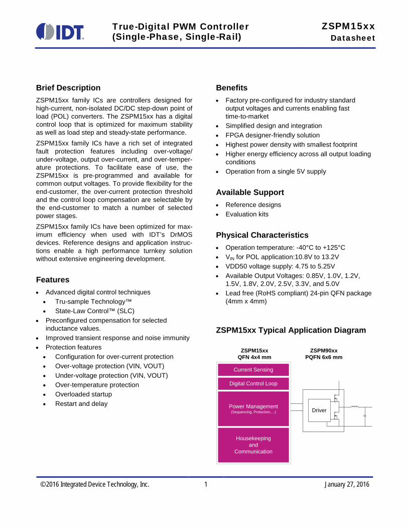
Brief Description ZSPM15xx family ICs are controllers designed for high-current, non-isolated DC/DC step-down point of load (POL) converters. The ZSPM15xx has a digital control loop that is optimized for maximum stability as well as load step and steady-state performance. ZSPM15xx family ICs have a rich set of integrated fault protection features including over-voltage/ under-voltage, output over-current, and over-temper-ature protections. To facilitate ease of use, the ZSPM15xx is pre-programmed and available for common output voltages. To provide flexibility for the end-customer, the over-current protection threshold and the control loop compensation are selectable by the end-customer to match a number of selected power stages. ZSPM15xx family ICs have been optimized for max-imum efficiency when used with IDT’s DrMOS devices. Reference designs and application instruc-tions enable a high performance turnkey solution without extensive engineering development.
Features • Advanced digital control techniques
• Tru-sample Technology™ • State-Law Control™ (SLC)
• Preconfigured compensation for selected inductance values.
• Improved transient response and noise immunity • Protection features
• Configuration for over-current protection • Over-voltage protection (VIN, VOUT) • Under-voltage protection (VIN, VOUT) • Over-temperature protection • Overloaded startup • Restart and delay
Benefits • Factory pre-configured for industry standard
output voltages and currents enabling fast time-to-market
• Simplified design and integration • FPGA designer-friendly solution • Highest power density with smallest footprint • Higher energy efficiency across all output loading
conditions • Operation from a single 5V supply
Available Support • Reference designs • Evaluation kits
Physical Characteristics • Operation temperature: -40°C to +125°C • VIN for POL application:10.8V to 13.2V • VDD50 voltage supply: 4.75 to 5.25V • Available Output Voltages: 0.85V, 1.0V, 1.2V,
1.5V, 1.8V, 2.0V, 2.5V, 3.3V, and 5.0V • Lead free (RoHS compliant) 24-pin QFN package
(4mm x 4mm)
ZSPM15xx Typical Application Diagram
Driver
ZSPM15xxQFN 4x4 mm
ZSPM90xxPQFN 6x6 mm
Current Sensing
Digital Control Loop
Power Management(Sequencing, Protection,…)
Housekeeping and
Communication
Driver

True-Digital PWM Controller (Single-Phase, Single-Rail)
ZSPM15xx Datasheet
© 2016 Integrated Device Technology, Inc. 2 January 27, 2016
Typical Applications Telecom Switches
Servers and Storage
Base Stations
Network Routers
Industrial Applications
Single-Rail/Single-Phase Supplies for Processors, ASICs, FPGAs, DSPs
Sequencer
Configurable Error Handler
ClockGeneration
OV Detection
OC Detection
FLASH ADC
CPU Core NVM (OTP)
1.8V RegDigital
1.8V RegAnalog
VREF
VFBP
VFBN
VDD
50
AVDD18
VDD18
Adaptive Digital Controller
PWM
DRVENPWM
VFBDigital Control Loop
ISNSP
ISNSN
Current Sensing
HKADC
Int. Temp Sense
TEMP
Bias Current Source VREFP
3.3V Reg
ADC
VR
EF
GPIO
THSH
DN
PGO
OD
CO
NTR
OL
DAC
DAC
CurrentLimiting
Average Current Sensing
OT Detection
Vin OV/UV Detection
CONFIG0
CONFIG1
VIN
VDD33
Vout UV Detection
ZSPM15xx Block Diagram
Ordering Information
Product Code Description Package ZSPM1501ZA1W0 ZSPM1501 lead-free QFN24; output voltage: 0.85V; inductance: 330nH; temperature: -40°C to +125°C Reel
ZSPM1502ZA1W0 ZSPM1502 lead-free QFN24; output voltage: 1.00V; inductance: 330nH; temperature: -40°C to +125°C Reel
ZSPM1503ZA1W0 ZSPM1503 lead-free QFN24; output voltage: 1.20V; inductance: 330nH; temperature: -40°C to +125°C Reel
ZSPM1504ZA1W0 ZSPM1504 lead-free QFN24; output voltage: 1.50V; inductance: 470nH; temperature: -40°C to +125°C Reel
ZSPM1505ZA1W0 ZSPM1505 lead-free QFN24; output voltage: 1.80V; inductance: 470nH; temperature: -40°C to +125°C Reel
ZSPM1506ZA1W0 ZSPM1506 lead-free QFN24; output voltage: 2.00V; inductance: 470nH; temperature: -40°C to +125°C Reel
ZSPM1507ZA1W0 ZSPM1507 lead-free QFN24; output voltage: 2.50V; inductance: 1000nH; temperature: -40°C to +125°C Reel
ZSPM1508ZA1W0 ZSPM1508 lead-free QFN24; output voltage: 3.30V; inductance: 2200nH; temperature: -40°C to +125°C Reel
ZSPM1509ZA1W0 ZSPM1509 lead-free QFN24; output voltage: 5.00V; inductance: 2200nH; temperature: -40°C to +125°C Reel
ZSPM1511ZA1W0 ZSPM1511 lead-free QFN24; output voltage: 0.85V; inductance: 680nH; temperature: -40°C to +125°C Reel
ZSPM1512ZA1W0 ZSPM1512 lead-free QFN24; output voltage: 1.00V; inductance: 680nH; temperature: -40°C to +125°C Reel
ZSPM1513ZA1W0 ZSPM1513 lead-free QFN24; output voltage: 1.20V; inductance: 680nH; temperature: -40°C to +125°C Reel
Corporate Headquarters 6024 Silver Creek Valley Road San Jose, CA 95138 www.IDT.com
Sales 1-800-345-7015 or 408-284-8200 Fax: 408-284-2775 www.IDT.com/go/sales
Tech Support www.IDT.com/go/support
DISCLAIMER Integrated Device Technology, Inc. (IDT) reserves the right to modify the products and/or specifications described herein at any time, without notice, at IDT's sole discretion. Performance specifications and operating parameters of the described products are determined in an independent state and are not guaranteed to perform the same way when installed in customer products. The information contained herein is provided without representation or warranty of any kind, whether express or implied, including, but not limited to, the suitability of IDT's products for any particular purpose, an implied warranty of merchantability, or non-infringement of the intellectual property rights of others. This document is presented only as a guide and does not convey any license under intellectual property rights of IDT or any third parties. IDT's products are not intended for use in applications involving extreme environmental conditions or in life support systems or similar devices where the failure or malfunction of an IDT product can be reasonably expected to significantly affect the health or safety of users. Anyone using an IDT product in such a manner does so at their own risk, absent an express, written agreement by IDT. Integrated Device Technology, IDT and the IDT logo are trademarks or registered trademarks of IDT and its subsidiaries in the United States and other countries. Other trademarks used herein are the property of IDT or their respective third party owners. For datasheet type definitions and a glossary of common terms, visit www.idt.com/go/glossary. All contents of this document are copyright of Integrated Device Technology, Inc. All rights reserved.

ZSPM15xx Datasheet
© 2016 Integrated Device Technology, Inc. 3 January 27, 2016
Contents 1 IC Characteristics ........................................................................................................................................... 14
1.1. Absolute Maximum Ratings ..................................................................................................................... 14 1.2. Recommended Operating Conditions ..................................................................................................... 15 1.3. Electrical Parameters .............................................................................................................................. 15 1.4. Device-Specific System Parameters ....................................................................................................... 18
1.4.1. ZSPM1501 ........................................................................................................................................ 18 1.4.2. ZSPM1502 ........................................................................................................................................ 18 1.4.3. ZSPM1503 ........................................................................................................................................ 19 1.4.4. ZSPM1504 ........................................................................................................................................ 20 1.4.5. ZSPM1505 ........................................................................................................................................ 20 1.4.6. ZSPM1506 ........................................................................................................................................ 21 1.4.7. ZSPM1507 ........................................................................................................................................ 22 1.4.8. ZSPM1508 ........................................................................................................................................ 22 1.4.9. ZSPM1509 ........................................................................................................................................ 23 1.4.10. ZSPM1511 ........................................................................................................................................ 23 1.4.11. ZSPM1512 ........................................................................................................................................ 24 1.4.12. ZSPM1513 ........................................................................................................................................ 24
2 Product Summary ........................................................................................................................................... 25 2.1. Overview .................................................................................................................................................. 25 2.2. Pin Description......................................................................................................................................... 27 2.3. Available Packages ................................................................................................................................. 28
3 Functional Description .................................................................................................................................... 29 3.1. Power Supply Circuitry, Reference Decoupling, and Grounding ............................................................ 29 3.2. Reset/Start-up Behavior .......................................................................................................................... 29 3.3. Digital Power Control ............................................................................................................................... 29
3.3.1. Overview ........................................................................................................................................... 29 3.3.2. Output Voltage Feedback ................................................................................................................. 29 3.3.3. Digital Compensator ......................................................................................................................... 30 3.3.4. Power Sequencing and the CONTROL Pin ...................................................................................... 31
3.4. Fault Monitoring and Response Generation ............................................................................................ 32 3.4.1. Output Over/Under-Voltage .............................................................................................................. 32 3.4.2. Output Current Protection ................................................................................................................. 32 3.4.3. Input Voltage Protection .................................................................................................................... 33 3.4.4. Over-Temperature Protection ........................................................................................................... 33
4 Application Information ................................................................................................................................... 34 4.1. Application Schematic ............................................................................................................................. 34 4.2. Device-Specific Passive Components ..................................................................................................... 36 4.3. Output Voltage Feedback Components .................................................................................................. 38

ZSPM15xx Datasheet
© 2016 Integrated Device Technology, Inc. 4 January 27, 2016
4.4. DCR Current Sensing Components ........................................................................................................ 38 4.5. Input Voltage Sensing ............................................................................................................................. 39 4.6. External Temperature Sensing ................................................................................................................ 39 4.7. CONFIG0 – Over-Current Protection Threshold ..................................................................................... 40 4.8. CONFIG1 – Compensation Loop and Output Voltage Slew Rate ........................................................... 41
5 Typical Performance Data .............................................................................................................................. 46 5.1. ZSPM1501 – Typical Load Transient Response – Capacitor Range #1 – Comp0 ................................. 47 5.2. ZSPM1501 – Typical Load Transient Response – Capacitor Range #2 – Comp1 ................................. 48 5.3. ZSPM1501 – Typical Load Transient Response – Capacitor Range #3 – Comp2 ................................. 49 5.4. ZSPM1501 – Typical Load Transient Response – Capacitor Range #4 – Comp3 ................................. 50 5.5. ZSPM1502 – Typical Load Transient Response – Capacitor Range #1 – Comp0 ................................. 51 5.6. ZSPM1502 – Typical Load Transient Response – Capacitor Range #2 – Comp1 ................................. 52 5.7. ZSPM1502 – Typical Load Transient Response – Capacitor Range #3 – Comp2 ................................. 53 5.8. ZSPM1502 – Typical Load Transient Response – Capacitor Range #4 – Comp3 ................................. 54 5.9. ZSPM1503 – Typical Load Transient Response – Capacitor Range #1 – Comp0 ................................. 55 5.10. ZSPM1503 – Typical Load Transient Response – Capacitor Range #2 – Comp1 ................................. 56 5.11. ZSPM1503 – Typical Load Transient Response – Capacitor Range #3 – Comp2 ................................. 57 5.12. ZSPM1503 – Typical Load Transient Response – Capacitor Range #4 – Comp3 ................................. 58 5.13. ZSPM1504 – Typical Load Transient Response – Capacitor Range #1 – Comp0 ................................. 59 5.14. ZSPM1504 – Typical Load Transient Response – Capacitor Range #2 – Comp1 ................................. 60 5.15. ZSPM1504 – Typical Load Transient Response – Capacitor Range #3 – Comp2 ................................. 61 5.16. ZSPM1504 – Typical Load Transient Response – Capacitor Range #4 – Comp3 ................................. 62 5.17. ZSPM1505 – Typical Load Transient Response – Capacitor Range #1 – Comp0 ................................. 63 5.18. ZSPM1505 – Typical Load Transient Response – Capacitor Range #2 – Comp1 ................................. 64 5.19. ZSPM1505 – Typical Load Transient Response – Capacitor Range #3 – Comp2 ................................. 65 5.20. ZSPM1505 – Typical Load Transient Response – Capacitor Range #4 – Comp3 ................................. 66 5.21. ZSPM1506 – Typical Load Transient Response – Capacitor Range #1 – Comp0 ................................. 67 5.22. ZSPM1506 – Typical Load Transient Response – Capacitor Range #2 – Comp1 ................................. 68 5.23. ZSPM1506 – Typical Load Transient Response – Capacitor Range #3 – Comp2 ................................. 69 5.24. ZSPM1506 – Typical Load Transient Response – Capacitor Range #4 – Comp3 ................................. 70 5.25. ZSPM1507 – Typical Load Transient Response –Capacitor Range 1 – Comp0 .................................... 71 5.26. ZSPM1507 – Typical Load Transient Response –Capacitor Range 2 – Comp1 .................................... 72 5.27. ZSPM1507 – Typical Load Transient Response –Capacitor Range 3 – Comp2 .................................... 73 5.28. ZSPM1507 – Typical Load Transient Response –Capacitor Range 4 – Comp3 .................................... 74 5.29. ZSPM1508 – Typical Load Transient Response –Capacitor Range 1 – Comp0 .................................... 75 5.30. ZSPM1508 – Typical Load Transient Response –Capacitor Range 2 – Comp1 .................................... 76 5.31. ZSPM1508 – Typical Load Transient Response –Capacitor Range 3 – Comp2 .................................... 77 5.32. ZSPM1508 – Typical Load Transient Response –Capacitor Range 4 – Comp3 .................................... 78 5.33. ZSPM1509 – Typical Load Transient Response –Capacitor Range 1 – Comp0 .................................... 79

ZSPM15xx Datasheet
© 2016 Integrated Device Technology, Inc. 5 January 27, 2016
5.34. ZSPM1509 – Typical Load Transient Response –Capacitor Range 2 – Comp1 .................................... 80 5.35. ZSPM1509 – Typical Load Transient Response –Capacitor Range 3 – Comp2 .................................... 81 5.36. ZSPM1509 – Typical Load Transient Response –Capacitor Range 4 – Comp3 .................................... 82 5.37. ZSPM1511 – Typical Load Transient Response – Capacitor Range #1 – Comp0 ................................. 83 5.38. ZSPM1511 – Typical Load Transient Response – Capacitor Range #2 – Comp1 ................................. 84 5.39. ZSPM1511 – Typical Load Transient Response – Capacitor Range #3 – Comp2 ................................. 85 5.40. ZSPM1511 – Typical Load Transient Response – Capacitor Range #4 – Comp3 ................................. 86 5.41. ZSPM1512 – Typical Load Transient Response – Capacitor Range #1 – Comp0 ................................. 87 5.42. ZSPM1512 – Typical Load Transient Response – Capacitor Range #2 – Comp1 ................................. 88 5.43. ZSPM1512 – Typical Load Transient Response – Capacitor Range #3 – Comp2 ................................. 89 5.44. ZSPM1512 – Typical Load Transient Response – Capacitor Range #4 – Comp3 ................................. 90 5.45. ZSPM1513 – Typical Load Transient Response – Capacitor Range #1 – Comp0 ................................. 91 5.46. ZSPM1513 – Typical Load Transient Response – Capacitor Range #2 – Comp1 ................................. 92 5.47. ZSPM1513 – Typical Load Transient Response – Capacitor Range #3 – Comp2 ................................. 93 5.48. ZSPM1513 – Typical Load Transient Response – Capacitor Range #4 – Comp3 ................................. 94 5.49. Typical Efficiency Curves – ZSPM1502 with ZSPM9000, ZSPM9015, and ZSPM9060 DrMOS ........... 95 5.50. Typical Efficiency Curves – ZSPM9000 DrMOS with ZSPM1504, ZSPM1505, and ZSPM1506 ........... 96 5.51. Typical Efficiency Curves – ZSPM9000 and ZSPM9060 DrMOS with ZSPM1508 and ZSPM1509 ...... 97 5.52. Typical Efficiency Curves – ZSPM9000 and ZSPM9060 DrMOS with ZSPM1511, ZSPM1512,
and ZSPM1513 ........................................................................................................................................ 98 6 Mechanical Specifications .............................................................................................................................. 99 7 Ordering Information .................................................................................................................................... 100 8 Related Documents ...................................................................................................................................... 100 9 Glossary ....................................................................................................................................................... 101 10 Document Revision History .......................................................................................................................... 101
List of Figures Figure 2.1 Typical Application Circuit with a 5V Supply Voltage ..................................................................... 25 Figure 2.2 Block Diagram ................................................................................................................................ 26 Figure 2.3 Pin-out QFN24 Package ................................................................................................................ 28 Figure 3.1 Simplified Block Diagram of the Digital Compensation .................................................................. 30 Figure 3.2 Power Sequencing ......................................................................................................................... 31 Figure 4.1 ZSPM15xx – Application Circuit with a 5V Supply Voltage ........................................................... 34 Figure 4.2 Output Voltage Sense Circuitry ...................................................................................................... 38 Figure 4.3 Inductor Current Sensing Using the DCR Method ......................................................................... 38 Figure 4.4 Input Voltage Sense Circuitry ......................................................................................................... 39 Figure 4.5 External Temperature Sense Circuitry ........................................................................................... 39 Figure 5.1 ZSPM1501 with Comp0; 5A to 15A Load Step; and Min. Capacitance ......................................... 47
ZSPM15xx Datasheet
© 2016 Integrated Device Technology, Inc. 6 January 27, 2016
Figure 5.2 ZSPM1501 with Comp0; 15A to 5A Load Step; and Min. Capacitance ......................................... 47 Figure 5.3 ZSPM1501 with Comp0; 5A to 15A Load Step; and Max. Capacitance ........................................ 47 Figure 5.4 ZSPM1501 with Comp0; 15A to 5A Load Step; and Max. Capacitance ........................................ 47 Figure 5.5 Open Loop Bode Plots for ZSPM1501 with Comp0....................................................................... 47 Figure 5.6 ZSPM1501 with Comp1; 5A to 15A Load Step; and Min. Capacitance ......................................... 48 Figure 5.7 ZSPM1501 with Comp1; 15A to 5A Load Step; and Min. Capacitance ......................................... 48 Figure 5.8 ZSPM1501 with Comp1; 5A to 15A Load Step; and Max. Capacitance ........................................ 48 Figure 5.9 ZSPM1501 with Comp1; 15A to 5A Load Step; and Max. Capacitance ........................................ 48 Figure 5.10 Open Loop Bode Plots for ZSPM1501 with Comp1....................................................................... 48 Figure 5.11 ZSPM1501 with Comp2; 5A to 15A Load Step; and Min. Capacitance ......................................... 49 Figure 5.12 ZSPM1501 with Comp2; 15A to 5A Load Step; and Min. Capacitance ......................................... 49 Figure 5.13 ZSPM1501 with Comp2; 5A to 15A Load Step; and Max. Capacitance ........................................ 49 Figure 5.14 ZSPM1501 with Comp2; 15A to 5A Load Step; and Max. Capacitance ........................................ 49 Figure 5.15 Open Loop Bode Plots for ZSPM1501 with Comp2....................................................................... 49 Figure 5.16 ZSPM1501 with Comp3; 5A to 15A Load Step; and Min. Capacitance ......................................... 50 Figure 5.17 ZSPM1501 with Comp3; 15A to 5A Load Step; and Min. Capacitance ......................................... 50 Figure 5.18 ZSPM1501 with Comp3; 5A to 15A Load Step; and Max. Capacitance ........................................ 50 Figure 5.19 ZSPM1501 with Comp3; 15A to 5A Load Step; and Max. Capacitance ........................................ 50 Figure 5.20 Open Loop Bode Plots for ZSPM1501 with Comp3....................................................................... 50 Figure 5.21 ZSPM1502 with Comp0; 5A to 15A Load Step; and Min. Capacitance ......................................... 51 Figure 5.22 ZSPM1502 with Comp0; 15A to 5A Load Step; and Min. Capacitance ......................................... 51 Figure 5.23 ZSPM1502 with Comp0; 5A to 15A Load Step; and Max. Capacitance ........................................ 51 Figure 5.24 ZSPM1502 with Comp0; 15A to 5A Load Step; and Max. Capacitance ........................................ 51 Figure 5.25 Open Loop Bode Plots for ZSPM1502 with Comp0....................................................................... 51 Figure 5.26 ZSPM1502 with Comp1; 5A to 15A Load Step; and Min. Capacitance ......................................... 52 Figure 5.27 ZSPM1502 with Comp1; 15A to 5A Load Step; and Min. Capacitance ......................................... 52 Figure 5.28 ZSPM1502 with Comp1; 5A to 15A Load Step; and Max. Capacitance ........................................ 52 Figure 5.29 ZSPM1502 with Comp1; 15A to 5A Load Step; and Max. Capacitance ........................................ 52 Figure 5.30 Open Loop Bode Plots for ZSPM1502 with Comp1....................................................................... 52 Figure 5.31 ZSPM1502 with Comp2; 5A to 15A Load Step; and Min. Capacitance ......................................... 53 Figure 5.32 ZSPM1502 with Comp2; 15A to 5A Load Step; and Min. Capacitance ......................................... 53 Figure 5.33 ZSPM1502 with Comp2; 5A to 15A Load Step; and Max. Capacitance ........................................ 53 Figure 5.34 ZSPM1502 with Comp2; 15A to 5A Load Step; and Max. Capacitance ........................................ 53 Figure 5.35 Open Loop Bode Plots for ZSPM1502 with Comp2....................................................................... 53 Figure 5.36 ZSPM1502 with Comp3; 5A to 15A Load Step; and Min. Capacitance ......................................... 54 Figure 5.37 ZSPM1502 with Comp3; 15A to 5A Load Step; and Min. Capacitance ......................................... 54 Figure 5.38 ZSPM1502 with Comp3; 5A to 15A Load Step; and Max. Capacitance ........................................ 54 Figure 5.39 ZSPM1502 with Comp3; 15A to 5A Load Step; and Max. Capacitance ........................................ 54 Figure 5.40 Open Loop Bode Plots for ZSPM1502 with Comp3....................................................................... 54
ZSPM15xx Datasheet
© 2016 Integrated Device Technology, Inc. 7 January 27, 2016
Figure 5.41 ZSPM1503 with Comp0; 5A to 15A Load Step; and Min. Capacitance ......................................... 55 Figure 5.42 ZSPM1503 with Comp0; 15A to 5A Load Step; and Min. Capacitance ......................................... 55 Figure 5.43 ZSPM1503 with Comp0; 5A to 15A Load Step; and Max. Capacitance ........................................ 55 Figure 5.44 ZSPM1503 with Comp0; 15A to 5A Load Step; and Max. Capacitance ........................................ 55 Figure 5.45 Open Loop Bode Plots for ZSPM1503 with Comp0....................................................................... 55 Figure 5.46 ZSPM1503 with Comp1; 5A to 15A Load Step; and Min. Capacitance ......................................... 56 Figure 5.47 ZSPM1503 with Comp1; 15A to 5A Load Step; and Min. Capacitance ......................................... 56 Figure 5.48 ZSPM1503 with Comp1; 5 to 15A Load Step; and Max. Capacitance .......................................... 56 Figure 5.49 ZSPM1503 with Comp1; 15 to 5A Load Step; and Max. Capacitance .......................................... 56 Figure 5.50 Open Loop Bode Plots for ZSPM1503 with Comp1....................................................................... 56 Figure 5.51 ZSPM1503 with Comp2; 5A to 15A Load Step; and Min. Capacitance ......................................... 57 Figure 5.52 ZSPM1503 with Comp2; 15A to 5A Load Step; and Min. Capacitance ......................................... 57 Figure 5.53 ZSPM1503 with Comp2; 5A to 15A Load Step; and Max. Capacitance ........................................ 57 Figure 5.54 ZSPM1503 with Comp2; 15A to 5A Load Step; and Max. Capacitance ........................................ 57 Figure 5.55 Open Loop Bode Plots for ZSPM1503 with Comp2....................................................................... 57 Figure 5.56 ZSPM1503 with Comp3; 5A to 15A Load Step; and Min. Capacitance ......................................... 58 Figure 5.57 ZSPM1503 with Comp3; 15A to 5A Load Step; and Min. Capacitance ......................................... 58 Figure 5.58 ZSPM1503 with Comp3; 5A to 15A Load Step; and Max. Capacitance ........................................ 58 Figure 5.59 ZSPM1503 with Comp3; 15A to 5A Load Step; and Max. Capacitance ........................................ 58 Figure 5.60 Open Loop Bode Plots for ZSPM1503 with Comp3....................................................................... 58 Figure 5.61 ZSPM1504 with Comp0; 5A to 15A Load Step; and Min. Capacitance ......................................... 59 Figure 5.62 ZSPM1504 with Comp0; 15A to 5A Load Step; and Min. Capacitance ......................................... 59 Figure 5.63 ZSPM1504 with Comp0; 5A to 15A Load Step; and Max. Capacitance ........................................ 59 Figure 5.64 ZSPM1504 with Comp0; 15A to 5A Load Step; and Max. Capacitance ........................................ 59 Figure 5.65 Open Loop Bode Plots for ZSPM1504 with Comp0....................................................................... 59 Figure 5.66 ZSPM1504 with Comp1; 5A to 15A Load Step; and Min. Capacitance ......................................... 60 Figure 5.67 ZSPM1504 with Comp1; 15A to 5A Load Step; and Min. Capacitance ......................................... 60 Figure 5.68 ZSPM1504 with Comp1; 5A to 15A Load Step; and Max. Capacitance ........................................ 60 Figure 5.69 ZSPM1504 with Comp1; 15A to 5A Load Step; and Max. Capacitance ........................................ 60 Figure 5.70 Open Loop Bode Plots for ZSPM1504 with Comp1....................................................................... 60 Figure 5.71 ZSPM1504 with Comp2; 5A to 15A Load Step; and Min. Capacitance ......................................... 61 Figure 5.72 ZSPM1504 with Comp2; 15A to 5A Load Step; and Min. Capacitance ......................................... 61 Figure 5.73 ZSPM1504 with Comp2; 5A to 15A Load Step; and Max. Capacitance ........................................ 61 Figure 5.74 ZSPM1504 with Comp2; 15A to 5A Load Step; and Max. Capacitance ........................................ 61 Figure 5.75 Open Loop Bode Plots for ZSPM1504 with Comp2....................................................................... 61 Figure 5.76 ZSPM1504 with Comp3; 5A to 15A Load Step; and Min. Capacitance ......................................... 62 Figure 5.77 ZSPM1504 with Comp3; 15A to 5A Load Step; and Min. Capacitance ......................................... 62 Figure 5.78 ZSPM1504 with Comp3; 5A to 15A Load Step; and Max. Capacitance ........................................ 62 Figure 5.79 ZSPM1504 with Comp3; 15A to 5A Load Step; and Max. Capacitance ........................................ 62
ZSPM15xx Datasheet
© 2016 Integrated Device Technology, Inc. 8 January 27, 2016
Figure 5.80 Open Loop Bode Plots for ZSPM1504 with Comp3....................................................................... 62 Figure 5.81 ZSPM1505 with Comp0; 5A to 15A Load Step; and Min. Capacitance ......................................... 63 Figure 5.82 ZSPM1505 with Comp0; 15A to 5A Load Step; and Min. Capacitance ......................................... 63 Figure 5.83 ZSPM1505 with Comp0; 5A to 15A Load Step; and Max. Capacitance ........................................ 63 Figure 5.84 ZSPM1505 with Comp0; 15A to 5A Load Step; and Max. Capacitance ........................................ 63 Figure 5.85 Open Loop Bode Plots for ZSPM1505 with Comp0....................................................................... 63 Figure 5.86 ZSPM1505 with Comp1; 5A to 15A Load Step; and Min. Capacitance ......................................... 64 Figure 5.87 ZSPM1505 with Comp1; 15A to 5A Load Step; and Min. Capacitance ......................................... 64 Figure 5.88 ZSPM1505 with Comp1; 5A to 15A Load Step; and Max. Capacitance ........................................ 64 Figure 5.89 ZSPM1505 with Comp1; 15A to 5A Load Step; and Max. Capacitance ........................................ 64 Figure 5.90 Open Loop Bode Plots for ZSPM1505 with Comp1....................................................................... 64 Figure 5.91 ZSPM1505 with Comp2; 5A to 15A Load Step; and Min. Capacitance ......................................... 65 Figure 5.92 ZSPM1505 with Comp2; 15A to 5A Load Step; and Min. Capacitance ......................................... 65 Figure 5.93 ZSPM1505 with Comp2; 5A to 15A Load Step; and Max. Capacitance ........................................ 65 Figure 5.94 ZSPM1505 with Comp2; 15A to 5A Load Step; and Max. Capacitance ........................................ 65 Figure 5.95 Open Loop Bode Plots for ZSPM1505 with Comp2....................................................................... 65 Figure 5.96 ZSPM1505 with Comp3; 5A to 15A Load Step; and Min. Capacitance ......................................... 66 Figure 5.97 ZSPM1505 with Comp3; 15A to 5A Load Step; and Min. Capacitance ......................................... 66 Figure 5.98 ZSPM1505 with Comp3; 5A to 15A Load Step; and Max. Capacitance ........................................ 66 Figure 5.99 ZSPM1505 with Comp3; 15A to 5A Load Step; and Max. Capacitance ........................................ 66 Figure 5.100 Open Loop Bode Plots for ZSPM1505 with Comp3....................................................................... 66 Figure 5.101 ZSPM1506 with Comp0; 5A to 15A Load Step; and Min. Capacitance ......................................... 67 Figure 5.102 ZSPM1506 with Comp0; 15A to 5A Load Step; and Min. Capacitance ......................................... 67 Figure 5.103 ZSPM1506 with Comp0; 5A to 15A Load Step; and Max. Capacitance ........................................ 67 Figure 5.104 ZSPM1506 with Comp0; 15A to 5A Load Step; and Max. Capacitance ........................................ 67 Figure 5.105 Open Loop Bode Plots for ZSPM1506 with Comp0....................................................................... 67 Figure 5.106 ZSPM1506 with Comp1; 5A to 15A Load Step; and Min. Capacitance ......................................... 68 Figure 5.107 ZSPM1506 with Comp1; 15A to 5A Load Step; and Min. Capacitance ......................................... 68 Figure 5.108 ZSPM1506 with Comp1; 5A to 15A Load Step; and Max. Capacitance ........................................ 68 Figure 5.109 ZSPM1506 with Comp1; 15A to 5A Load Step; and Max. Capacitance ........................................ 68 Figure 5.110 Open Loop Bode Plots for ZSPM1506 with Comp1....................................................................... 68 Figure 5.111 ZSPM1506 with Comp2; 5A to 15A Load Step; and Min. Capacitance ......................................... 69 Figure 5.112 ZSPM1506 with Comp2; 15A to 5A Load Step; and Min. Capacitance ......................................... 69 Figure 5.113 ZSPM1506 with Comp2; 5A to 15A Load Step; and Max. Capacitance ........................................ 69 Figure 5.114 ZSPM1506 with Comp2; 15A to 5A Load Step; and Max. Capacitance ........................................ 69 Figure 5.115 Open Loop Bode Plots for ZSPM1506 with Comp2....................................................................... 69 Figure 5.116 ZSPM1506 with Comp3; 5A to 15A Load Step; and Min. Capacitance ......................................... 70 Figure 5.117 ZSPM1506 with Comp3; 15A to 5A Load Step; and Min. Capacitance ......................................... 70

ZSPM15xx Datasheet
© 2016 Integrated Device Technology, Inc. 9 January 27, 2016
Figure 5.118 ZSPM1506 with Comp3; 5A to 15A Load Step; and Max. Capacitance ........................................ 70 Figure 5.119 ZSPM1506 with Comp3; 15A to 5A Load Step; and Max. Capacitance ........................................ 70 Figure 5.120 Open Loop Bode Plots for ZSPM1506 with Comp3....................................................................... 70 Figure 5.121 ZSPM1507 with Comp0; 5 to 15A Load Step; and Min. Capacitance ........................................... 71 Figure 5.122 ZSPM1507 with Comp0; 15 to 5A Load Step; and Min. Capacitance ........................................... 71 Figure 5.123 ZSPM1507 with Comp0; 5 to 15A Load Step; and Max. Capacitance .......................................... 71 Figure 5.124 ZSPM1507 with Comp0; 15 to 5A Load Step; and Max. Capacitance .......................................... 71 Figure 5.125 Open Loop Bode Plots for ZSPM1507 with Comp0....................................................................... 71 Figure 5.126 ZSPM1507 with Comp1; 5 to 15A Load Step; and Min. Capacitance ........................................... 72 Figure 5.127 ZSPM1507 with Comp1; 15 to 5A Load Step; and Min. Capacitance ........................................... 72 Figure 5.128 ZSPM1507 with Comp1; 5 to 15A Load Step; and Max. Capacitance .......................................... 72 Figure 5.129 ZSPM1507 with Comp1; 15 to 5A Load Step; and Max. Capacitance .......................................... 72 Figure 5.130 Open Loop Bode Plots for ZSPM1507 with Comp1....................................................................... 72 Figure 5.131 ZSPM1507 with Comp2; 5 to 15A Load Step; and Min. Capacitance ........................................... 73 Figure 5.132 ZSPM1507 with Comp2; 15 to 5A Load Step; and Min. Capacitance ........................................... 73 Figure 5.133 ZSPM1507 with Comp2; 5 to 15A Load Step; and Max. Capacitance .......................................... 73 Figure 5.134 ZSPM1507 with Comp2; 15 to 5A Load Step; and Max. Capacitance .......................................... 73 Figure 5.135 Open Loop Bode Plots for ZSPM1507 with Comp2....................................................................... 73 Figure 5.136 ZSPM1507 with Comp3; 5 to 15A Load Step; and Min. Capacitance ........................................... 74 Figure 5.137 ZSPM1507 with Comp3; 15 to 5A Load Step; and Min. Capacitance ........................................... 74 Figure 5.138 ZSPM1507 with Comp3; 5 to 15A Load Step; and Max. Capacitance .......................................... 74 Figure 5.139 ZSPM1507 with Comp3; 15 to 5A Load Step; and Max. Capacitance .......................................... 74 Figure 5.140 Open Loop Bode Plots for ZSPM1507 with Comp3....................................................................... 74 Figure 5.141 ZSPM1508 with Comp0; 5A to 10A Load Step; and Min. Capacitance ......................................... 75 Figure 5.142 ZSPM1508 with Comp0; 10A to 5A Load Step; and Min. Capacitance ......................................... 75 Figure 5.143 ZSPM1508 with Comp0; 5A to 10A Load Step; and Max. Capacitance ........................................ 75 Figure 5.144 ZSPM1508 with Comp0; 10A to 5A Load Step; and Max. Capacitance ........................................ 75 Figure 5.145 Open Loop Bode Plots for ZSPM1508 with Comp0....................................................................... 75 Figure 5.146 ZSPM1508 with Comp1; 5A to 10A Load Step; and Min. Capacitance ......................................... 76 Figure 5.147 ZSPM1508 with Comp1; 10A to 5A Load Step; and Min. Capacitance ......................................... 76 Figure 5.148 ZSPM1508 with Comp1; 5A to 10A Load Step; and Max. Capacitance ........................................ 76 Figure 5.149 ZSPM1508 with Comp1; 10A to 5A Load Step; and Max. Capacitance ........................................ 76 Figure 5.150 Open Loop Bode Plots for ZSPM1508 with Comp1....................................................................... 76 Figure 5.151 ZSPM1508 with Comp2; 5A to 10A Load Step; and Min. Capacitance ......................................... 77 Figure 5.152 ZSPM1508 with Comp2; 10A to 5A Load Step; and Min. Capacitance ......................................... 77 Figure 5.153 ZSPM1508 with Comp2; 5A to 10A Load Step; and Max. Capacitance ........................................ 77 Figure 5.154 ZSPM1508 with Comp2; 10A to 5A Load Step; and Max. Capacitance ........................................ 77 Figure 5.155 Open Loop Bode Plots for ZSPM1508 with Comp2....................................................................... 77 Figure 5.156 ZSPM1508 with Comp3; 5A to 10A Load Step; and Min. Capacitance ......................................... 78

ZSPM15xx Datasheet
© 2016 Integrated Device Technology, Inc. 10 January 27, 2016
Figure 5.157 ZSPM1508 with Comp3; 10A to 5A Load Step; and Min. Capacitance ......................................... 78 Figure 5.158 ZSPM1508 with Comp3; 5A to 10A Load Step; and Max. Capacitance ........................................ 78 Figure 5.159 ZSPM1508 with Comp3; 10A to 5A Load Step; and Max. Capacitance ........................................ 78 Figure 5.160 Open Loop Bode Plots for ZSPM1508 with Comp3....................................................................... 78 Figure 5.161 ZSPM1509 with Comp0; 3A to 8A Load Step; and Min. Capacitance ........................................... 79 Figure 5.162 ZSPM1509 with Comp0; 8A to 3A Load Step; and Min. Capacitance ........................................... 79 Figure 5.163 ZSPM1509 with Comp0; 3A to 8A Load Step; and Max. Capacitance .......................................... 79 Figure 5.164 ZSPM1509 with Comp0; 8A to 3A Load Step; and Max. Capacitance .......................................... 79 Figure 5.165 Open Loop Bode Plots for ZSPM1509 with Comp0....................................................................... 79 Figure 5.166 ZSPM1509 with Comp1; 3A to 8A Load Step; and Min. Capacitance ........................................... 80 Figure 5.167 ZSPM1509 with Comp1; 8A to 3A Load Step; and Min. Capacitance ........................................... 80 Figure 5.168 ZSPM1509 with Comp1; 3A to 8A Load Step; and Max. Capacitance .......................................... 80 Figure 5.169 ZSPM1509 with Comp1; 8A to 3A Load Step; and Max. Capacitance .......................................... 80 Figure 5.170 Open Loop Bode Plots for ZSPM1509 with Comp1....................................................................... 80 Figure 5.171 ZSPM1509 with Comp2; 3A to 8A Load Step; and Min. Capacitance ........................................... 81 Figure 5.172 ZSPM1509 with Comp2; 8A to 3A Load Step; and Min. Capacitance ........................................... 81 Figure 5.173 ZSPM1509 with Comp2; 3A to 8A Load Step; and Max. Capacitance .......................................... 81 Figure 5.174 ZSPM1509 with Comp2; 8A to 3A Load Step; and Max. Capacitance .......................................... 81 Figure 5.175 Open Loop Bode Plots for ZSPM1509 with Comp2....................................................................... 81 Figure 5.176 ZSPM1509 with Comp3; 3A to 8A Load Step; and Min. Capacitance ........................................... 82 Figure 5.177 ZSPM1509 with Comp3; 8A to 3A Load Step; and Min. Capacitance ........................................... 82 Figure 5.178 ZSPM1509 with Comp3; 3A to 8A Load Step; and Max. Capacitance .......................................... 82 Figure 5.179 ZSPM1509 with Comp3; 8A to 3A Load Step; and Max. Capacitance .......................................... 82 Figure 5.180 Open Loop Bode Plots for ZSPM1509 with Comp3....................................................................... 82 Figure 5.181 ZSPM1511 with Comp0; 5A to 15A Load Step; and Min. Capacitance ......................................... 83 Figure 5.182 ZSPM1511 with Comp0; 15A to 5A Load Step; and Min. Capacitance ......................................... 83 Figure 5.183 ZSPM1511 with Comp0; 5A to 15A Load Step; and Max. Capacitance ........................................ 83 Figure 5.184 ZSPM1511 with Comp0; 15A to 5A Load Step; and Max. Capacitance ........................................ 83 Figure 5.185 Open Loop Bode Plots for ZSPM1511 with Comp0....................................................................... 83 Figure 5.186 ZSPM1511 with Comp1; 5A to 15A Load Step; and Min. Capacitance ......................................... 84 Figure 5.187 ZSPM1511 with Comp1; 15A to 5A Load Step; and Min. Capacitance ......................................... 84 Figure 5.188 ZSPM1511 with Comp1; 5A to 15A Load Step; and Max. Capacitance ........................................ 84 Figure 5.189 ZSPM1511 with Comp1; 15A to 5A Load Step; and Max. Capacitance ........................................ 84 Figure 5.190 Open Loop Bode Plots for ZSPM1511 with Comp1....................................................................... 84 Figure 5.191 ZSPM1511 with Comp2; 5A to 15A Load Step; and Min. Capacitance ......................................... 85 Figure 5.192 ZSPM1511 with Comp2; 15A to 5A Load Step; and Min. Capacitance ......................................... 85 Figure 5.193 ZSPM1511 with Comp2; 5A to 15A Load Step; and Max. Capacitance ........................................ 85 Figure 5.194 ZSPM1511 with Comp2; 15A to 5A Load Step; and Max. Capacitance ........................................ 85 Figure 5.195 Open Loop Bode Plots for ZSPM1511 with Comp2....................................................................... 85

ZSPM15xx Datasheet
© 2016 Integrated Device Technology, Inc. 11 January 27, 2016
Figure 5.196 ZSPM1511 with Comp3; 5A to 15A Load Step; and Min. Capacitance ......................................... 86 Figure 5.197 ZSPM1511 with Comp3; 15A to 5A Load Step; and Min. Capacitance ......................................... 86 Figure 5.198 ZSPM1511 with Comp3; 5A to 15A Load Step; and Max. Capacitance ........................................ 86 Figure 5.199 ZSPM1511 with Comp3; 15A to 5A Load Step; and Max. Capacitance ........................................ 86 Figure 5.200 Open Loop Bode Plots for ZSPM1511 with Comp3....................................................................... 86 Figure 5.201 ZSPM1512 with Comp0; 5A to 15A Load Step; and Min. Capacitance ......................................... 87 Figure 5.202 ZSPM1512 with Comp0; 15A to 5A Load Step; and Min. Capacitance ......................................... 87 Figure 5.203 ZSPM1512 with Comp0; 5A to 15A Load Step; and Max. Capacitance ........................................ 87 Figure 5.204 ZSPM1512 with Comp0; 15A to 5A Load Step; and Max. Capacitance ........................................ 87 Figure 5.205 Open Loop Bode Plots for ZSPM1512 with Comp0....................................................................... 87 Figure 5.206 ZSPM1512 with Comp1; 5A to 15A Load Step; and Min. Capacitance ......................................... 88 Figure 5.207 ZSPM1512 with Comp1; 15A to 5A Load Step; and Min. Capacitance ......................................... 88 Figure 5.208 ZSPM1512 with Comp1; 5A to 15A Load Step; and Max. Capacitance ........................................ 88 Figure 5.209 ZSPM1512 with Comp1; 15A to 5A Load Step; and Max. Capacitance ........................................ 88 Figure 5.210 Open Loop Bode Plots for ZSPM1512 with Comp1....................................................................... 88 Figure 5.211 ZSPM1512 with Comp2; 5A to 15A Load Step; and Min. Capacitance ......................................... 89 Figure 5.212 ZSPM1512 with Comp2; 15A to 5A Load Step; and Min. Capacitance ......................................... 89 Figure 5.213 ZSPM1512 with Comp2; 5A to 15A Load Step; and Max. Capacitance ........................................ 89 Figure 5.214 ZSPM1512 with Comp2; 15A to 5A Load Step; and Max. Capacitance ........................................ 89 Figure 5.215 Open Loop Bode Plots for ZSPM1512 with Comp2....................................................................... 89 Figure 5.216 ZSPM1512 with Comp3; 5A to 15A Load Step; and Min. Capacitance ......................................... 90 Figure 5.217 ZSPM1512 with Comp3; 15A to 5A Load Step; and Min. Capacitance ......................................... 90 Figure 5.218 ZSPM1512 with Comp3; 5A to 15A Load Step; and Max. Capacitance ........................................ 90 Figure 5.219 ZSPM1512 with Comp3; 15A to 5A Load Step; and Max. Capacitance ........................................ 90 Figure 5.220 Open Loop Bode Plots for ZSPM1512 with Comp3....................................................................... 90 Figure 5.221 ZSPM1513 with Comp0; 5A to 15A Load Step; and Min. Capacitance ......................................... 91 Figure 5.222 ZSPM1513 with Comp0; 15A to 5A Load Step; and Min. Capacitance ......................................... 91 Figure 5.223 ZSPM1513 with Comp0; 5A to 15A Load Step; and Max. Capacitance ........................................ 91 Figure 5.224 ZSPM1513 with Comp0; 15A to 5A Load Step; and Max. Capacitance ........................................ 91 Figure 5.225 Open Loop Bode Plots for ZSPM1513 with Comp0....................................................................... 91 Figure 5.226 ZSPM1513 with Comp1; 5A to 15A Load Step; and Min. Capacitance ......................................... 92 Figure 5.227 ZSPM1513 with Comp1; 15A to 5A Load Step; and Min. Capacitance ......................................... 92 Figure 5.228 ZSPM1513 with Comp1; 5 to 15A Load Step; and Max. Capacitance .......................................... 92 Figure 5.229 ZSPM1513 with Comp1; 15 to 5A Load Step; and Max. Capacitance .......................................... 92 Figure 5.230 Open Loop Bode Plots for ZSPM1513 with Comp1....................................................................... 92 Figure 5.231 ZSPM1513 with Comp2; 5A to 15A Load Step; and Min. Capacitance ......................................... 93 Figure 5.232 ZSPM1513 with Comp2; 15A to 5A Load Step; and Min. Capacitance ......................................... 93 Figure 5.233 ZSPM1513 with Comp2; 5A to 15A Load Step; and Max. Capacitance ........................................ 93 Figure 5.234 ZSPM1513 with Comp2; 15A to 5A Load Step; and Max. Capacitance ........................................ 93 Figure 5.235 Open Loop Bode Plots for ZSPM1513 with Comp2....................................................................... 93 Figure 5.236 ZSPM1513 with Comp3; 5A to 15A Load Step; and Min. Capacitance ......................................... 94 Figure 5.237 ZSPM1513 with Comp3; 15A to 5A Load Step; and Min. Capacitance ......................................... 94

ZSPM15xx Datasheet
© 2016 Integrated Device Technology, Inc. 12 January 27, 2016
Figure 5.238 ZSPM1513 with Comp3; 5A to 15A Load Step; and Max. Capacitance ........................................ 94 Figure 5.239 ZSPM1513 with Comp3; 15A to 5A Load Step; and Max. Capacitance ........................................ 94 Figure 5.240 Open Loop Bode Plots for ZSPM1513 with Comp3....................................................................... 94 Figure 5.241 Typical Efficiency Curves: ZSPM1502 with ZSPM9000, ZSPM9015, and ZSPM9060 DrMOS
(VIN= 12V; Vout = 1.0V) .................................................................................................................. 95 Figure 5.242 Typical Efficiency Curves: ZSPM9000 DrMOS with ZSPM1504, ZSPM1505, and ZSPM1506
(VIN = 12V) ...................................................................................................................................... 96 Figure 5.243 Typical Efficiency Curves: ZSPM9000 and ZSPM9060 DrMOS with ZSPM1508 and ZSPM150997 Figure 5.244 Typical Efficiency Curves: ZSPM9000 and ZSPM9060 DrMOS with ZSPM1511, ZSPM1512,
and ZSPM1513 .............................................................................................................................. 98 Figure 6.1 24-Pin QFN Package Drawing ....................................................................................................... 99

ZSPM15xx Datasheet
© 2016 Integrated Device Technology, Inc. 13 January 27, 2016
List of Tables Table 2.1 ZSPM15xx Pin Descriptions ........................................................................................................... 27 Table 3.1 Fault Configuration Overview ......................................................................................................... 32 Table 4.1 Passive Component Values for the Application Circuits ................................................................ 35 Table 4.2 Passive Components for the ZSPM1501, ZSPM1502, and ZSPM1503 ....................................... 36 Table 4.3 Passive Components for the ZSPM1504, ZSPM1505, and ZSPM1506 ....................................... 36 Table 4.4 Passive Components for the ZSPM1507 ....................................................................................... 37 Table 4.5 Passive Components for the ZSPM1508 and ZSPM1509 ............................................................. 37 Table 4.6 Passive Components for the ZSPM1511, ZSPM1512, and ZSPM1513 ....................................... 37 Table 4.7 ZSPM15xx – OCP Pin Strap Resistor Selection ............................................................................ 40 Table 4.8 Recommended Output Capacitor Ranges ..................................................................................... 41 Table 4.9 Compensator and VOUT Slew Rate Pin Strap Resistor Selection for the ZSPM1501 to
ZSPM1506 and the ZSPM1511 to ZSPM1513 .............................................................................. 42 Table 4.10 Compensator and VOUT Slew Rate Pin Strap Resistor Selection for the ZSPM1507 .................. 43 Table 4.11 Compensator and VOUT Slew Rate Pin Strap Resistor Selection for the ZSPM1508 .................. 44 Table 4.12 Compensator and VOUT Slew Rate Pin Strap Resistor Selection for the ZSPM1509 .................. 45
ZSPM15xx Datasheet
© 2016 Integrated Device Technology, Inc. 14 January 27, 2016
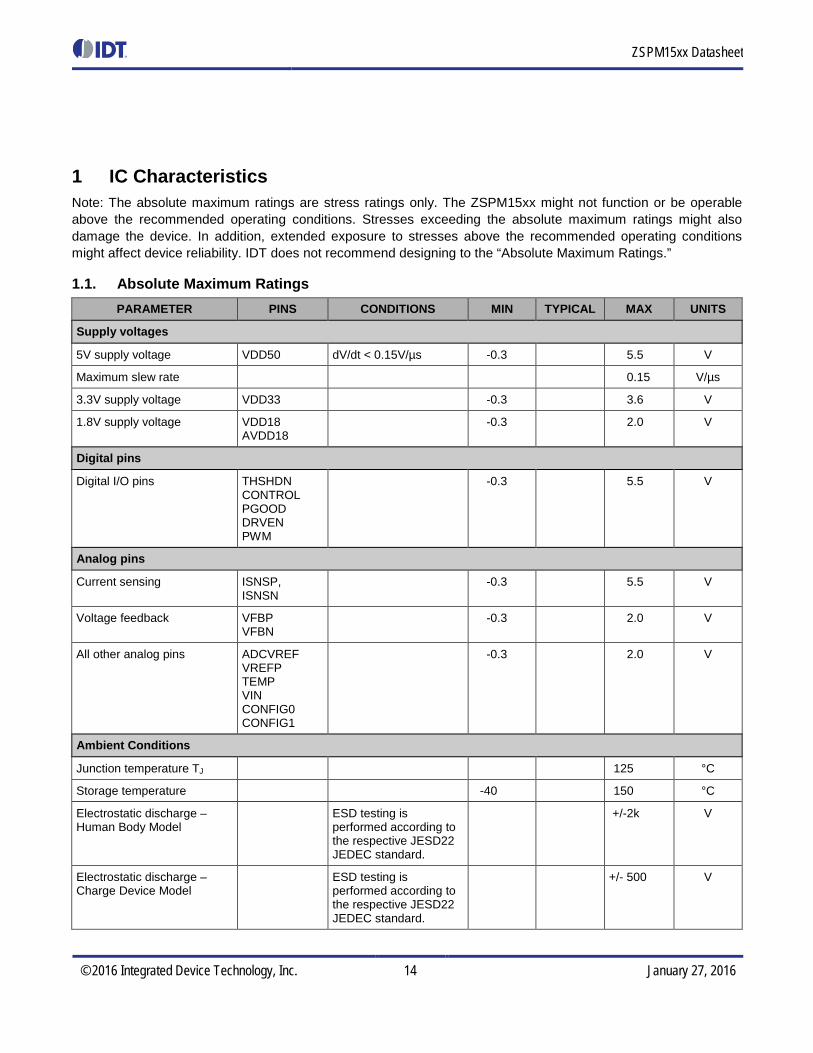
1 IC Characteristics Note: The absolute maximum ratings are stress ratings only. The ZSPM15xx might not function or be operable above the recommended operating conditions. Stresses exceeding the absolute maximum ratings might also damage the device. In addition, extended exposure to stresses above the recommended operating conditions might affect device reliability. IDT does not recommend designing to the “Absolute Maximum Ratings.”
1.1. Absolute Maximum Ratings PARAMETER PINS CONDITIONS MIN TYPICAL MAX UNITS
Supply voltages
5V supply voltage VDD50 dV/dt < 0.15V/µs -0.3 5.5 V
Maximum slew rate 0.15 V/µs
3.3V supply voltage VDD33 -0.3 3.6 V
1.8V supply voltage VDD18 AVDD18
-0.3 2.0 V
Digital pins
Digital I/O pins THSHDN CONTROL PGOOD DRVEN PWM
-0.3 5.5 V
Analog pins
Current sensing ISNSP, ISNSN
-0.3 5.5 V
Voltage feedback VFBP VFBN
-0.3 2.0 V
All other analog pins ADCVREF VREFP TEMP VIN CONFIG0 CONFIG1
-0.3 2.0 V
Ambient Conditions
Junction temperature TJ 125 °C
Storage temperature -40 150 °C
Electrostatic discharge – Human Body Model
ESD testing is performed according to the respective JESD22 JEDEC standard.
+/-2k V
Electrostatic discharge – Charge Device Model
ESD testing is performed according to the respective JESD22 JEDEC standard.
+/- 500 V

ZSPM15xx Datasheet
© 2016 Integrated Device Technology, Inc. 15 January 27, 2016
1.2. Recommended Operating Conditions PARAMETER SYMBOL CONDITIONS MIN TYPICAL MAX UNITS
Ambient conditions
Operation temperature TJ -40 125 °C
Thermal resistance junction to ambient
θJA 40 K/W
1.3. Electrical Parameters PARAMETER SYMBOL CONDITIONS MIN TYPICAL MAX UNITS
Supply voltages
5V supply voltage VVDD50 4.75 5.0 5.25 V
5V supply current IVDD50 VDD50=5.0V 23 mA
3.3V supply voltage VVDD33 Supply for both the VDD33 and VDD50 pins if the internal 3.3V regulator is not used.
3.0 3.3 3.6 V
3.3V supply current IVDD33 VDD50=VDD33=3.3V 23 mA
Internally generated supply voltages
3.3V supply voltage VVDD33 VDD50=5.0V 3.0 3.3 3.6 V
3.3V output current IVDD33 VDD50=5.0V 2.0 mA
1.8V supply voltages VAVDD18 VVDD18
VDD50=5.0V 1.72 1.80 1.98 V
1.8V output current 0 mA
Power-on reset (POR)
Power-on reset threshold – on VTH_POR_ON 2.8 V
Power-on reset threshold – off VTH_POR_OFF 2.6 V
Initialization period / internal startup time
5 ms
Digital IO pins (CONTROL, PGOOD, DRVEN, THSHDN)
Input high voltage VDD33=3.3V 2.0 V
Input low voltage VDD33=3.3V 0.8 V
Output high voltage VDD33=3.3V 2.4 VDD33 V
Output low voltage 0.5 V
Input leakage current ±1.0 µA
Output current – high 2.0 mA
Output current – low 2.0 mA
ZSPM15xx Datasheet
© 2016 Integrated Device Technology, Inc. 16 January 27, 2016
PARAMETER SYMBOL CONDITIONS MIN TYPICAL MAX UNITS
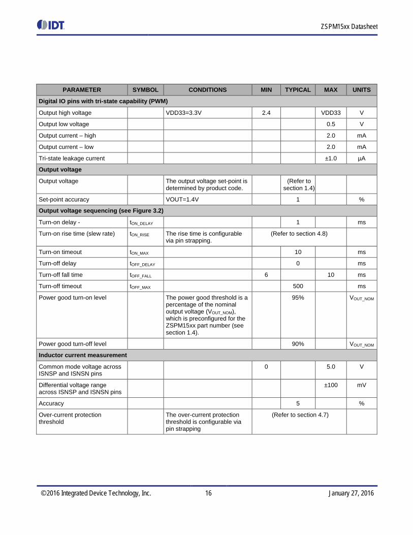
Digital IO pins with tri-state capability (PWM)
Output high voltage VDD33=3.3V 2.4 VDD33 V
Output low voltage 0.5 V
Output current – high 2.0 mA
Output current – low 2.0 mA
Tri-state leakage current ±1.0 µA
Output voltage
Output voltage The output voltage set-point is determined by product code.
(Refer to section 1.4)
Set-point accuracy VOUT=1.4V 1 %
Output voltage sequencing (see Figure 3.2)
Turn-on delay - tON_DELAY 1 ms
Turn-on rise time (slew rate) tON_RISE The rise time is configurable via pin strapping.
(Refer to section 4.8)
Turn-on timeout tON_MAX 10 ms
Turn-off delay tOFF_DELAY 0 ms
Turn-off fall time tOFF_FALL 6 10 ms
Turn-off timeout tOFF_MAX 500 ms
Power good turn-on level The power good threshold is a percentage of the nominal output voltage (VOUT_NOM), which is preconfigured for the ZSPM15xx part number (see section 1.4).
95% VOUT_NOM
Power good turn-off level 90% VOUT_NOM
Inductor current measurement
Common mode voltage across ISNSP and ISNSN pins
0 5.0 V
Differential voltage range across ISNSP and ISNSN pins
±100 mV
Accuracy 5 %
Over-current protection threshold
The over-current protection threshold is configurable via pin strapping
(Refer to section 4.7)

ZSPM15xx Datasheet
© 2016 Integrated Device Technology, Inc. 17 January 27, 2016
PARAMETER SYMBOL CONDITIONS MIN TYPICAL MAX UNITS
Digital pulse width modulator
Switching frequency fSW 500 kHz
Resolution 163 ps
Frequency accuracy 2.0 %
Duty cycle 2.5 100 %
External temperature measurement (note: only PN-junction sense elements are supported)
Offset voltage at 25°C 583 mV
Temperature coefficient -2.2 mV/K
Bias currents for external temperature sensing
60 µA
Accuracy of measurement ±5.0 K
Over-temperature threshold 105 °C
Internal temperature measurement
Accuracy of measurement ±5.0 K
Over-temperature threshold 95 °C
ZSPM15xx Datasheet
© 2016 Integrated Device Technology, Inc. 18 January 27, 2016
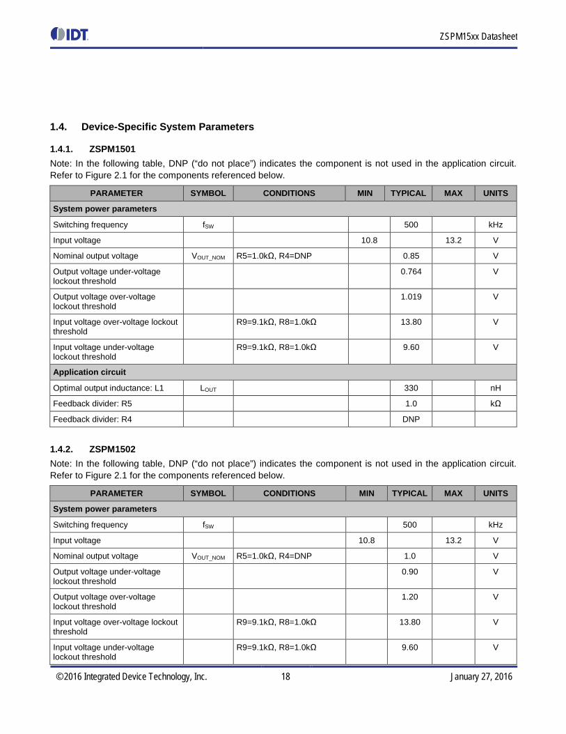
1.4. Device-Specific System Parameters
1.4.1. ZSPM1501 Note: In the following table, DNP (“do not place”) indicates the component is not used in the application circuit. Refer to Figure 2.1 for the components referenced below.
PARAMETER SYMBOL CONDITIONS MIN TYPICAL MAX UNITS
System power parameters
Switching frequency fSW 500 kHz
Input voltage 10.8 13.2 V
Nominal output voltage VOUT_NOM R5=1.0kΩ, R4=DNP 0.85 V
Output voltage under-voltage lockout threshold
0.764 V
Output voltage over-voltage lockout threshold
1.019 V
Input voltage over-voltage lockout threshold
R9=9.1kΩ, R8=1.0kΩ 13.80 V
Input voltage under-voltage lockout threshold
R9=9.1kΩ, R8=1.0kΩ 9.60 V
Application circuit
Optimal output inductance: L1 LOUT 330 nH
Feedback divider: R5 1.0 kΩ
Feedback divider: R4 DNP
1.4.2. ZSPM1502 Note: In the following table, DNP (“do not place”) indicates the component is not used in the application circuit. Refer to Figure 2.1 for the components referenced below.
PARAMETER SYMBOL CONDITIONS MIN TYPICAL MAX UNITS
System power parameters
Switching frequency fSW 500 kHz
Input voltage 10.8 13.2 V
Nominal output voltage VOUT_NOM R5=1.0kΩ, R4=DNP 1.0 V
Output voltage under-voltage lockout threshold
0.90 V
Output voltage over-voltage lockout threshold
1.20 V
Input voltage over-voltage lockout threshold
R9=9.1kΩ, R8=1.0kΩ 13.80 V
Input voltage under-voltage lockout threshold
R9=9.1kΩ, R8=1.0kΩ 9.60 V

ZSPM15xx Datasheet
© 2016 Integrated Device Technology, Inc. 19 January 27, 2016
PARAMETER SYMBOL CONDITIONS MIN TYPICAL MAX UNITS
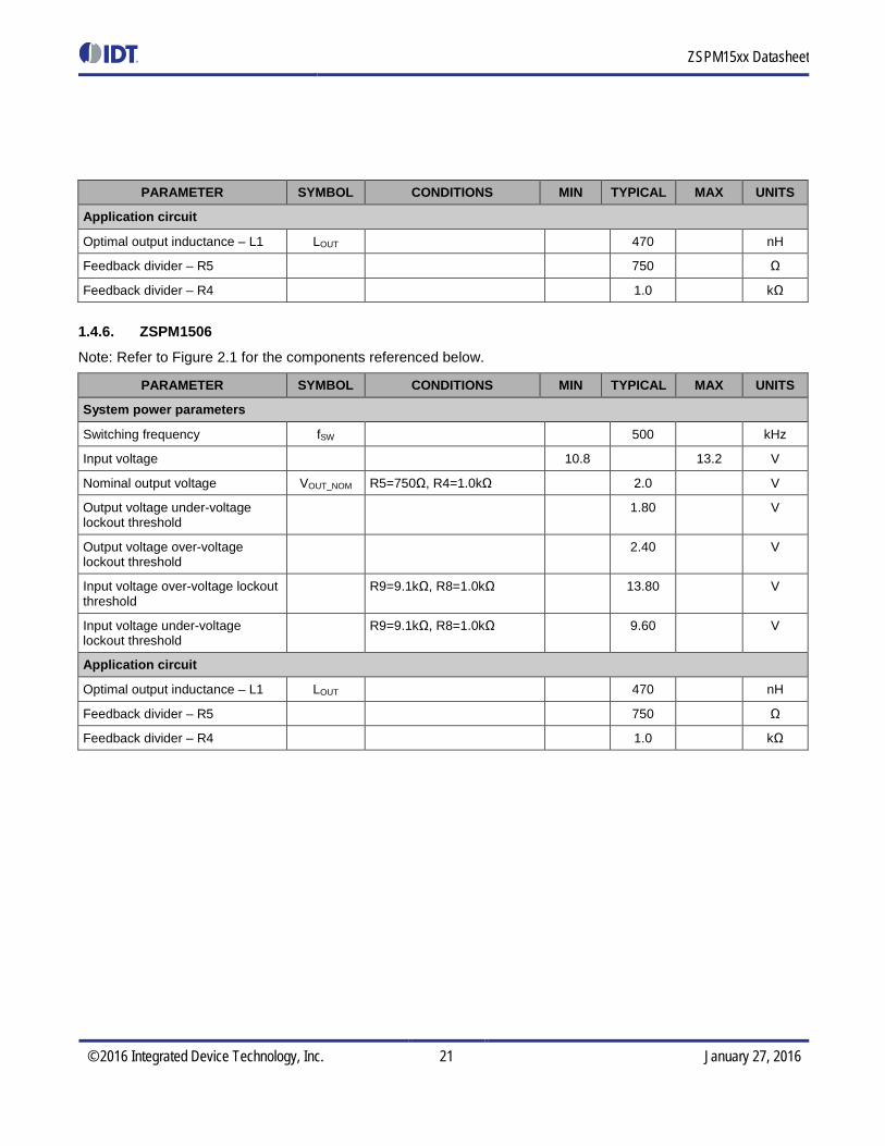
Application circuit
Optimal output inductance – L1 LOUT 330 nH
Feedback divider – R5 1.0 kΩ
Feedback divider – R4 DNP
1.4.3. ZSPM1503 Note: In the following table, DNP (“do not place”) indicates the component is not used in the application circuit. Refer to Figure 2.1 for the components referenced below.
PARAMETER SYMBOL CONDITIONS MIN TYPICAL MAX UNITS
System power parameters
Switching frequency fSW 500 kHz
Input voltage 10.8 13.2 V
Nominal output voltage VOUT_NOM R5=1.0kΩ, R4=DNP 1.20 V
Output voltage under-voltage lockout threshold
1.08 V
Output voltage over-voltage lockout threshold
1.44 V
Input voltage over-voltage lockout threshold
R9=9.1kΩ, R8=1.0kΩ 13.80 V
Input voltage under-voltage lockout threshold
R9=9.1kΩ, R8=1.0kΩ 9.60 V
Application circuit
Optimal output inductance – L1 LOUT 330 nH
Feedback divider – R5 1.0 kΩ
Feedback divider – R4 DNP

ZSPM15xx Datasheet
© 2016 Integrated Device Technology, Inc. 20 January 27, 2016
1.4.4. ZSPM1504 Note: Refer to Figure 2.1 for the components referenced below.
PARAMETER SYMBOL CONDITIONS MIN TYPICAL MAX UNITS
System power parameters
Switching frequency fSW 500 kHz
Input voltage 10.8 13.2 V
Nominal output voltage VOUT_NOM R5=750Ω, R4=1.0kΩ 1.5 V
Output voltage under-voltage lockout threshold
1.35 V
Output voltage over-voltage lockout threshold
1.80 V
Input voltage over-voltage lockout threshold
R9=9.1kΩ, R8=1.0kΩ 13.80 V
Input voltage under-voltage lockout threshold
R9=9.1kΩ, R8=1.0kΩ 9.60 V
Application circuit
Optimal output inductance – L1 LOUT 470 nH
Feedback divider – R5 750 Ω
Feedback divider – R4 1.0 kΩ
1.4.5. ZSPM1505
Note: Refer to Figure 2.1 for the components referenced below.
PARAMETER SYMBOL CONDITIONS MIN TYPICAL MAX UNITS
System power parameters
Switching frequency fSW 500 kHz
Input voltage 10.8 13.2 V
Nominal output voltage VOUT_NOM R5=750Ω, R4=1.0kΩ 1.8 V
Output voltage under-voltage lockout threshold
1.62 V
Output voltage over-voltage lockout threshold
2.16 V
Input voltage over-voltage lockout threshold
R9=9.1kΩ, R8=1.0kΩ 13.80 V
Input voltage under-voltage lockout threshold
R9=9.1kΩ, R8=1.0kΩ 9.60 V
ZSPM15xx Datasheet
© 2016 Integrated Device Technology, Inc. 21 January 27, 2016
PARAMETER SYMBOL CONDITIONS MIN TYPICAL MAX UNITS
Application circuit
Optimal output inductance – L1 LOUT 470 nH
Feedback divider – R5 750 Ω
Feedback divider – R4 1.0 kΩ
1.4.6. ZSPM1506
Note: Refer to Figure 2.1 for the components referenced below.
PARAMETER SYMBOL CONDITIONS MIN TYPICAL MAX UNITS
System power parameters
Switching frequency fSW 500 kHz
Input voltage 10.8 13.2 V
Nominal output voltage VOUT_NOM R5=750Ω, R4=1.0kΩ 2.0 V
Output voltage under-voltage lockout threshold
1.80 V
Output voltage over-voltage lockout threshold
2.40 V
Input voltage over-voltage lockout threshold
R9=9.1kΩ, R8=1.0kΩ 13.80 V
Input voltage under-voltage lockout threshold
R9=9.1kΩ, R8=1.0kΩ 9.60 V
Application circuit
Optimal output inductance – L1 LOUT 470 nH
Feedback divider – R5 750 Ω
Feedback divider – R4 1.0 kΩ

ZSPM15xx Datasheet
© 2016 Integrated Device Technology, Inc. 22 January 27, 2016
1.4.7. ZSPM1507
PARAMETER SYMBOL CONDITIONS MIN TYPICAL MAX UNITS
System power parameters
Switching frequency fSW 500 kHz
Input voltage 10.8 12 13.2 V
Nominal output voltage VOUT_NOM R5=1.0kΩ, R4=1.0kΩ 2.5V V
Output voltage under-voltage lockout threshold
2.25 V
Output voltage over-voltage lockout threshold
3.0 V
Input voltage over-voltage lockout threshold
R9=9.1kΩ, R8=1.0kΩ 13.8 V
Input voltage under-voltage lockout threshold
R9=9.1kΩ, R8=1.0kΩ 9.6 V
Application circuit
Optimal output inductance: L1 LOUT 1000 nH
Feedback divider: R5 1.0 kΩ
Feedback divider: R4 1.0 kΩ
1.4.8. ZSPM1508
PARAMETER SYMBOL CONDITIONS MIN TYPICAL MAX UNITS
System power parameters
Switching frequency fSW 500 kHz
Input voltage 10.8 13.2 V
Nominal output voltage VOUT_NOM R5=3.3kΩ, R4=1.0kΩ 3.3 V
Output voltage under-voltage lockout threshold
2.97 V
Output voltage over-voltage lockout threshold
3.96 V
Input voltage over-voltage lockout threshold
R9=9.1kΩ, R8=1.0kΩ 13.80 V
Input voltage under-voltage lockout threshold
R9=9.1kΩ, R8=1.0kΩ 9.60 V
Application circuit
Optimal output inductance: L1 LOUT 2.20 µH
Feedback divider: R5 3.3 kΩ
Feedback divider: R4 1.0 kΩ

ZSPM15xx Datasheet
© 2016 Integrated Device Technology, Inc. 23 January 27, 2016
1.4.9. ZSPM1509
PARAMETER SYMBOL CONDITIONS MIN TYPICAL MAX UNITS
System power parameters
Switching frequency fSW 500 kHz
Input voltage 10.8 13.2 V
Nominal output voltage VOUT_NOM R5=3.3k Ω, R4=1.0kΩ 5.0 V
Output voltage under-voltage lockout threshold
4.50 V
Output voltage over-voltage lockout threshold
5.50 V
Input voltage over-voltage lockout threshold
R9=9.1kΩ, R8=1.0kΩ 13.80 V
Input voltage under-voltage lockout threshold
R9=9.1kΩ, R8=1.0kΩ 9.60 V
Application circuit
Optimal output inductance: L1 LOUT 2.20 µH
Feedback divider: R5 3.3 kΩ
Feedback divider: R4 1.0 kΩ
1.4.10. ZSPM1511 Note: In the following table, DNP (“do not place”) indicates the component is not used in the application circuit.
PARAMETER SYMBOL CONDITIONS MIN TYPICAL MAX UNITS
System power parameters
Switching frequency fSW 500 kHz
Input voltage 10.8 13.2 V
Nominal output voltage VOUT_NOM R5=1.0k Ω, R4=DNP 0.85 V
Output voltage under-voltage lockout threshold
0.764 V
Output voltage over-voltage lockout threshold
1.019 V
Input voltage over-voltage lockout threshold
R9=9.1 kΩ, R8=1.0kΩ 13.80 V
Input voltage under-voltage lockout threshold
R9=9.1 kΩ, R8=1.0kΩ 9.60 V
Application circuit
Optimal output inductance – L1 LOUT 680 ƞH
Feedback divider – R5 1.0 kΩ
Feedback divider – R4 DNP

ZSPM15xx Datasheet
© 2016 Integrated Device Technology, Inc. 24 January 27, 2016
1.4.11. ZSPM1512 Note: In the following table, DNP (“do not place”) indicates the component is not used in the application circuit.
PARAMETER SYMBOL CONDITIONS MIN TYPICAL MAX UNITS
System power parameters
Switching frequency fSW 500 kHz
Input voltage 10.8 13.2 V
Nominal output voltage VOUT_NOM R5=1.0k Ω, R4=DNP 1.0 V
Output voltage under-voltage lockout threshold
0.90 V
Output voltage over-voltage lockout threshold
1.20 V
Input voltage over-voltage lockout threshold
R9=9.1 kΩ, R8=1.0kΩ 13.80 V
Input voltage under-voltage lockout threshold
R9=9.1 kΩ, R8=1.0kΩ 9.60 V
Application circuit
Optimal output inductance – L1 LOUT 680 ƞH
Feedback divider – R5 1.0 kΩ
Feedback divider – R4 DNP kΩ
1.4.12. ZSPM1513 Note: In the following table, DNP (“do not place”) indicates the component is not used in the application circuit.
PARAMETER SYMBOL CONDITIONS MIN TYPICAL MAX UNITS
System power parameters
Switching frequency fSW 500 kHz
Input voltage 10.8 13.2 V
Nominal output voltage VOUT_NOM R5=1.0k Ω, R4=DNP 1.20 V
Output voltage under-voltage lockout threshold
1.08 V
Output voltage over-voltage lockout threshold
1.44 V
Input voltage over-voltage lockout threshold
R9=9.1 kΩ, R8=1.0kΩ 13.80 V
Input voltage under-voltage lockout threshold
R9=9.1 kΩ, R8=1.0kΩ 9.60 V
Application circuit
Optimal output inductance – L1 LOUT 680 ƞH
Feedback divider – R5 1.0 kΩ
Feedback divider – R4 DNP kΩ

ZSPM15xx Datasheet
© 2016 Integrated Device Technology, Inc. 25 January 27, 2016
2 Product Summary 2.1. Overview The ZSPM15xx is a configurable true-digital single-phase PWM controller for high-current, non-isolated DC/DC supplies. It incorporates a pre-configured digital control loop, which is optimized for different power stages, bundled with output voltage sensing, average inductor current sensing, and extensive fault monitoring and handling options.
Several different functional units are incorporated in the device. A dedicated digital control loop is used to provide fast loop response and optimal output voltage regulation. This includes output voltage sensing, average inductor current sensing, a digital control law, and a digital pulse-width modulator (DPWM). In parallel, a dedicated, configurable error handler allows fast detection of error signals and their appropriate handling. A housekeeping analog-to-digital converter (HKADC) ensures the reliable and efficient measurement of environmental signals, such as input voltage and temperature.
An application-specific, low-power integrated microcontroller is used to control the overall system. It manages configuration of the various logic units according to the preprogrammed configuration look-up tables and the external configuration resistors connected to the CONFIG0 and CONFIG1 pins. These pin-strapping resistors expedite configuration of the over-current protection threshold, compensation, and output voltage slew rate. A high-reliability, high-temperature one-time programmable memory (OTP) is used to store configuration parameters. All required bias and reference voltages are internally derived from the external supply voltage.
Figure 2.1 Typical Application Circuit with a 5V Supply Voltage
DrMOS
+5V
+Vout
PGND
Vin
C1,C2,C3
C4,C5,C6
R1
R2,R3
R4
R7,C8
R9
C10,R8
R5
R6, C9
C7
ZSPM15xx
CONTROLPGOOD
CONFIG1CONFIG0
AGND
ADCVREF
VREFPAVDD18
VDD18
VDD50VDD33
GND
VIN
TEMP
PWMDRVEN
ISNSPISNSN
VFBPVFBN
CoutCin
D1
L1
C11
THSHDN
ZSPM15xx Datasheet
© 2016 Integrated Device Technology, Inc. 26 January 27, 2016
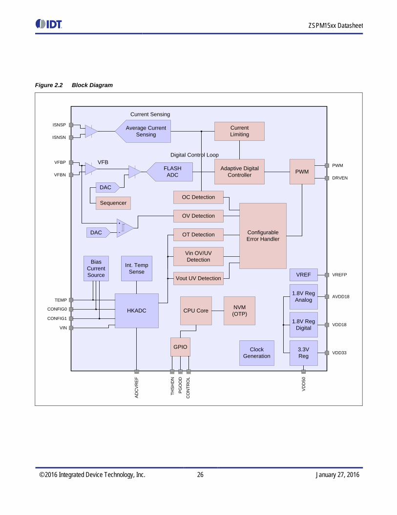
Figure 2.2 Block Diagram
Sequencer
Configurable Error Handler
ClockGeneration
OV Detection
OC Detection
FLASH ADC
CPU Core NVM (OTP)
1.8V RegDigital
1.8V RegAnalog
VREF
VFBP
VFBN
VDD
50AVDD18
VDD18
Adaptive Digital Controller
PWM
DRVENPWM
VFBDigital Control Loop
ISNSP
ISNSN
Current Sensing
HKADC
Int. Temp Sense
TEMP
Bias Current Source VREFP
3.3V Reg
ADC
VR
EF
GPIO
THSH
DN
PGO
OD
CO
NTR
OL
DAC
DAC
CurrentLimiting
Average Current Sensing
OT Detection
Vin OV/UV Detection
CONFIG0
CONFIG1
VIN
VDD33
Vout UV Detection

ZSPM15xx Datasheet
© 2016 Integrated Device Technology, Inc. 27 January 27, 2016
2.2. Pin Description Table 2.1 ZSPM15xx Pin Descriptions
Pin Name Direction Type Description
1 AGND Input Supply Analog Ground
2 VREFP Output Supply Reference Terminal
3 VFBP Input Analog Positive Input of Differential Feedback Voltage Sensing
4 VFBN Input Analog Negative Input of Differential Feedback Voltage Sensing
5 ISNSP Input Analog Positive Input of Differential Current Sensing
6 ISNSN Input Analog Negative Input of Differential Current Sensing
7 TEMP Input Analog Connection to External Temperature Sensing Element
8 VIN Input Analog Power Supply Input Voltage Sensing
9 CONFIG0 Input Analog Configuration Selection 0
10 CONFIG1 Input Analog Configuration Selection 1
11 PWM Output Digital High-side FET Control Signal
12 DRVEN Output Digital Driver Enable Signal
13 PGOOD Output Digital PGOOD Output (Internal Pull-Down)
14 CONTROL Input Digital Control Input
15 THSHDN Input Digital Thermal-Shut Down Input from Power Stage
16 N.C. No connection – pin must be allowed to float
17 N.C. No connection – pin must be allowed to float
18 N.C. No connection – pin must be allowed to float
19 GND Input Supply Digital Ground
20 VDD18 Output Supply Internal 1.8V Digital Supply Terminal
21 VDD33 Input/Output Supply 3.3V Supply Voltage Terminal
22 VDD50 Input Supply 5.0V Supply Voltage Terminal
23 AVDD18 Output Supply Internal 1.8V Analog Supply Terminal
24 ADCVREF Input Analog Analog-to-Digital Converter (ADC) Reference Terminal
PAD PAD Input Supply Exposed PAD, Digital Ground
ZSPM15xx Datasheet
© 2016 Integrated Device Technology, Inc. 28 January 27, 2016
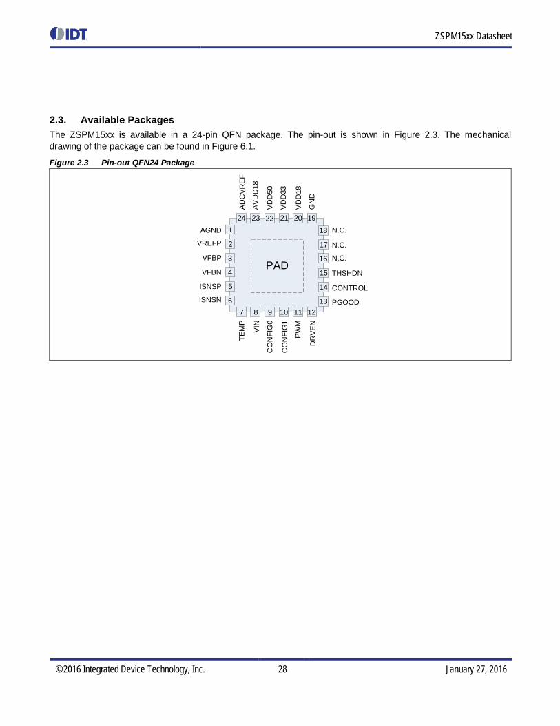
2.3. Available Packages The ZSPM15xx is available in a 24-pin QFN package. The pin-out is shown in Figure 2.3. The mechanical drawing of the package can be found in Figure 6.1.
Figure 2.3 Pin-out QFN24 Package
ADC
VREF
AVD
D18
VDD
50
V DD
33
VDD
18
GN
D
PAD
1920212224 23
ISNSP
ISNSN
VFBP
VFBN
AGND
4
2
1
3
5
6
VREFP
PWM
DR
VEN
VIN
TEM
P
CO
NFI
G0
CO
NFI
G1
7 8 12109 11
CONTROL
PGOOD
N.C.
N.C.
N.C.
13
14
15
16
18
17
THSHDN
ZSPM15xx Datasheet
© 2016 Integrated Device Technology, Inc. 29 January 27, 2016
3 Functional Description 3.1. Power Supply Circuitry, Reference Decoupling, and Grounding The ZSPM15xx incorporates several internal power regulators in order to derive all required supply and bias voltages from a single external supply voltage of 5.0V. Decoupling capacitors are required at the VDD33, VDD18, and AVDD18 pins (1.0µF minimum; 4.7µF recommended).
The reference voltages required for operation are generated within the ZSPM15xx. External decoupling must be provided between the VREFP and ADCVREF pins. Therefore, a 4.7µF capacitor is required at the VREFP pin and a 100nF capacitor at ADCVREF pin. The two pins should be connected with approximately 50Ω resistance in order to provide sufficient decoupling between the pins.
Three different ground connections are available on the outside of the package. These should be connected together to a single ground tie. A differentiation between analog and digital ground is not required.
3.2. Reset/Start-up Behavior The ZSPM15xx employs an internal power-on-reset (POR) circuit to ensure proper start-up and shut-down with a changing supply voltage. Once the supply voltage increases above the POR threshold voltage (see section 1.3), the ZSPM15xx begins the internal start-up process. Upon its completion, the device is ready for operation.
3.3. Digital Power Control
3.3.1. Overview The digital power control loop consists of the integral parts required for the control functionality of the ZSPM15xx. A high-speed analog front-end is used to digitize the output voltage. A digital control core uses the acquired information to provide duty-cycle information to the PWM, which controls the drive signals to the power stage.
See section 7 for the pre-configured nominal output voltages for the different part codes available in the ZSPM15xx family.
3.3.2. Output Voltage Feedback The voltage feedback signal is sampled with a high-speed analog front-end. The feedback voltage is differentially measured and subtracted from an internal voltage reference using an error amplifier. A flash ADC is then used to convert the voltage into its digital equivalent. This is followed by internal digital filtering to improve the system’s noise rejection.
For some applications, an external feedback divider (R4 and R5; see Figure 4.1) is required to allow for output voltage operations above the internal reference voltage. For details, refer to the application section 4.3.

ZSPM15xx Datasheet
© 2016 Integrated Device Technology, Inc. 30 January 27, 2016
3.3.3. Digital Compensator The sampled output voltage is processed by a digital control loop in order to modulate the DPWM output signals controlling the power stage. This digital control loop works as a voltage-mode controller using a PID-type compensation. The basic structure of the controller is shown in Figure 3.1. The proprietary State-Law™ Control (SLC) concept features two parallel compensators for steady-state operation and fast transient operation. This allows tuning the compensators individually for the respective needs; i.e., quiet steady state and fast transient performance. The ZSPM15xx implements fast, reliable switching between the different compensation modes in order to ensure good transient performance and a quiet steady state.
Figure 3.1 Simplified Block Diagram of the Digital Compensation
Two techniques are used to improve transient performance further: • Tru-sample Technology™ is used to acquire fast, accurate, and continuous information about the output vol-
tage so that the device can react quickly to any change in output voltage. Tru-sample Technology™ reduces phase-lag caused by sampling delays, reduces noise sensitivity, and improves transient performance.
• A nonlinear gain adjustment is used during large load transients to boost the loop gain and reduce the settling time.
The control loops in the ZSPM15xx are preconfigured and can be selected using a pin-strapping option. A range of different output capacitors is supported. Refer to section 4.8 for detailed information.
Digital PID Compensator
Steady-state
Transient
Coefficients
Non-linearGain
Operation Mode
Detection
Digital Error Signal Duty Cycle

ZSPM15xx Datasheet
© 2016 Integrated Device Technology, Inc. 31 January 27, 2016
3.3.4. Power Sequencing and the CONTROL Pin The ZSPM15xx has a set of pre-configured power-sequencing features. The typical sequence of events is shown in Figure 3.2. The individual values for the delay (tON_DELAY and tOFF_DELAY), ramp time (tON_RISE and tOFF_FALL) and time-outs (tON_MAX and tOFF_MAX) are listed in section 1.3. Note that the device is slew-rate controlled for tON_RISE ramping via the pin-strapping options. The slew rate can be selected in the application circuit using the pin-strap options as explained in section 4.8. The CONTROL pin is pre-configured for active high operation.
The ZSPM15xx features a power good (PGOOD) output, which can be used to indicate the state of the power rail. If the output voltage level is above the power good ON threshold, the pin is set to active, indicating a stable output voltage on the rail.
Figure 3.2 Power Sequencing
ttON_DELAY tON_RISE
tON_MAX
tOFF_DELAY tOFF_FALL
0 V
VOUT_NOM
tOFF_MAX
CONTROL
VPGOOD_ONVPGOOD_OFF
PGOOD

ZSPM15xx Datasheet
© 2016 Integrated Device Technology, Inc. 32 January 27, 2016
3.4. Fault Monitoring and Response Generation The ZSPM15xx monitors various signals during operation and compares them with fault thresholds (see the “Threshold” column in Table 3.1). If a parameter exceeds a fault threshold, the respective fault signal is asserted and the ZSPM15xx will disable the output voltage as described below. Note that the ZSPM15xx features internal blanking times for voltage and temperature faults in order to improve noise-immunity.
Three different response types are supported by the ZSPM15xx. The “low-impedance” response turns off the top MOSFET and enables the low-side MOSFET; i.e., PWM=0. After tOFF_MAX, both MOSFETs will be turned off, PWM=Z, DRVEN=0. A “high-impedance” response will disable both MOSFETs instantaneously, PWM=Z. A “soft-off” response ramps the output voltage down, similar to a power-down operation via the CONTROL pin. After tOFF_MAX, the controller will disable the power stage by turning both switches off, PWM=Z, DRVEN=0. The ZSPM15xx features a “hiccup mode,” which allows it to re-enable its output voltage after the fault condition has been removed.
Table 3.1 Fault Configuration Overview
Fault Response Type Blanking Threshold
Output Over-Voltage Low-impedance 25µs Preconfigured; see section 1.4.
Output Under-Voltage High-impedance 450µs Preconfigured; see section 1.4.
Input Over-Voltage High-impedance 450µs Preconfigured; see section 1.4.
Input Under-Voltage High-impedance 450µs Preconfigured; see section 1.4.
Over-Current Low-impedance None Pin-strap selectable; see section 4.7.
Internal Over-Temperature Soft-off 5ms See specification in section 1.3.
External Over-Temperature Soft-off 5ms See specification in section 1.3.
3.4.1. Output Over/Under-Voltage To prevent damage to the load, the ZSPM15xx utilizes an output over-voltage protection circuit. The voltage at VFBP is continuously compared with a preconfigured threshold using a high-speed analog comparator. If the voltage exceeds the configured threshold, the fault response is generated.
The ZSPM15xx also monitors the output voltage with a lower threshold. If the output voltage falls below the under-voltage fault level, a fault event is generated. See section 1.4 for the device-specific threshold levels.
3.4.2. Output Current Protection The ZSPM15xx offers cycle-by-cycle average current sensing with configurable over-current protection. A dedicated ADC is used to provide fast and accurate current information over the switching period. The acquired information is compared with a selectable over-current threshold to detect faults. DCR current sensing across the inductor is supported. Additionally, the device uses DCR temperature compensation via the external temperature sense element. This increases the accuracy of the current sense method by counteracting the significant change of the DCR over temperature.
The ZSPM15xx continuously monitors the average inductor current and utilizes this information to protect the power supply against excessive output current. If the average inductor current exceeds the selected over-current fault threshold, the fault response will be generated. See section 4.7 for instructions for configuring the threshold.

ZSPM15xx Datasheet
© 2016 Integrated Device Technology, Inc. 33 January 27, 2016
3.4.3. Input Voltage Protection The ZSPM15xx continuously monitors the input voltage via the VIN pin. If the input voltage is outside an operation range defined by a lower and higher input voltage threshold, a fault is detected and a response generated. See section 1.4 for device-specific specifications for the thresholds.
3.4.4. Over-Temperature Protection The ZSPM15xx features two independent temperature measurement units for internal and external temperature measurement. The internal temperature sensing measures the temperatures inside the ZSPM15xx. Place the external temperature sense element close to the inductor to measure its temperature. Use a PN-junction as the external temperature sense element. Small-signal transistors, such the 3904, are widely used for this application. The ZSPM15xx monitors these internal and external temperature measurements. If either of the temperatures exceeds the over-temperature threshold (see section 1.3), the fault response will be generated. For additional information on the external temperature sensing, refer to section 4.6.

ZSPM15xx Datasheet
© 2016 Integrated Device Technology, Inc. 34 January 27, 2016
4 Application Information 4.1. Application Schematic
Figure 4.1 ZSPM15xx – Application Circuit with a 5V Supply Voltage
DrMOS
+5V
+Vout
PGND
Vin
C1,C2,C3
C4,C5,C6
R1
R2,R3
R4
R7,C8
R9
C10,R8
R5
R6, C9
C7
ZSPM15xx
CONTROLPGOOD
CONFIG1CONFIG0
AGND
ADCVREF
VREFPAVDD18
VDD18
VDD50VDD33
GND
VIN
TEMP
PWMDRVEN
ISNSPISNSN
VFBPVFBN
CoutCin
D1
L1
C11
THSHDN
ZSPM90xx
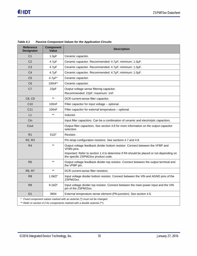
ZSPM15xx Datasheet
© 2016 Integrated Device Technology, Inc. 35 January 27, 2016
Table 4.1 Passive Component Values for the Application Circuits
Reference Designator
Component Value Description
C1 1.0µF Ceramic capacitor.
C2 4.7µF Ceramic capacitor. Recommended: 4.7µF; minimum: 1.0µF.
C3 4.7µF Ceramic capacitor. Recommended: 4.7µF; minimum: 1.0µF.
C4 4.7µF Ceramic capacitor. Recommended: 4.7µF; minimum: 1.0µF.
C5 4.7µF* Ceramic capacitor.
C6 100nF* Ceramic capacitor.
C7 22pF Output voltage sense filtering capacitor. Recommended: 22pF; maximum: 1nF.
C8, C9 ** DCR current-sense filter capacitor.
C10 100nF Filter capacitor for input voltage – optional.
C11 100nF Filter capacitor for external temperature – optional.
L1 ** Inductor.
Cin Input filter capacitors. Can be a combination of ceramic and electrolytic capacitors.
Cout . Output filter capacitors. See section 4.8 for more information on the output capacitor selection.
R1 51Ω* Resistor.
R2, R3 . Pin-strap configuration resistors. See sections 4.7 and 4.8.
R4 ** Output voltage feedback divider bottom resistor. Connect between the VFBP and VFBN pins. Important: Refer to section 1.4 to determine if R4 should be placed or not depending on the specific ZSPM15xx product code.
R5 ** Output voltage feedback divider top resistor. Connect between the output terminal and the VFBP pin.
R6, R7 ** DCR current-sense filter resistors.
R8 1.0kΩ* Input voltage divider bottom resistor. Connect between the VIN and AGND pins of the ZSPM15xx.
R9 9.1kΩ* Input voltage divider top resistor. Connect between the main power input and the VIN pin of the ZSPM15xx.
D1 3904 External temperature sense element (PN-junction). See section 4.6.
* Fixed component values marked with an asterisk (*) must not be changed. ** Refer to section 4.2 for components marked with a double asterisk (**).

ZSPM15xx Datasheet
© 2016 Integrated Device Technology, Inc. 36 January 27, 2016
4.2. Device-Specific Passive Components Each product in the ZSPM15xx family requires external device-specific passive components. These are listed in the following tables.
If specified in the following tables, the feedback divider (R4, R5) is mandatory to achieve the specified output voltage. The control loop has been optimized for the inductance specified, but inductors from different venders can be used. Note: The ZSPM15xx has been optimized for the specific Würth inductors recommended in the following tables depending on the ZSPM15xx product number. If a different inductor is used, its specifications should be comparable to the recommended Würth inductor; otherwise the full optimization provided by the ZSPM15xx might not be achieved. If a different inductor is used, the current sense components (R6, R7, C8) must be recalculated according to section 4.4.
Components specified as DNP must not be placed.
Table 4.2 Passive Components for the ZSPM1501, ZSPM1502, and ZSPM1503
Reference Designator Component Value Description
Feedback divider
R4 DNP Output voltage feedback divider bottom resistor. Important: Do not place R4 for the ZSPM1501, ZSPM1502, and ZSPM1503.
R5 1.0kΩ Output voltage feedback divider top resistor. Connect between the output terminal and the VFBP pin.
Inductor and current sensing
L1 L=330nH Recommended inductor: Würth WE-HCM 744301033.
R6, R7 1050Ω DCR current-sense filter resistors.
C8, C9 1000nF DCR current-sense filter capacitor.
Table 4.3 Passive Components for the ZSPM1504, ZSPM1505, and ZSPM1506
Reference Designator Component Value Description
Feedback divider
R4 1kΩ Output voltage feedback divider bottom resistor.
R5 750Ω Output voltage feedback divider top resistor. Connect between the output terminal and the VFBP pin.
Inductor and current sensing
L1 L=470nH Recommended inductor: Würth WE-HCM 744301047.
R6, R7 1000Ω DCR current-sense filter resistors.
C8, C9 1000nF DCR current-sense filter capacitor.

ZSPM15xx Datasheet
© 2016 Integrated Device Technology, Inc. 37 January 27, 2016
Table 4.4 Passive Components for the ZSPM1507
Reference Designator Component Value Description
Feedback divider
R4 1kΩ Output voltage feedback divider bottom resistor.
R5 1kΩ Output voltage feedback divider top resistor. Connect between the output terminal and the VFBP pin.
Inductor and current sensing
L1 L=1000nH Recommended inductor: Würth WE-HCM 7443310100.
R6, R7 1.05kΩ DCR current-sense filter resistors.
C8, C9 820nF DCR current-sense filter capacitor.
Table 4.5 Passive Components for the ZSPM1508 and ZSPM1509
Reference Designator Component Value Description
Feedback divider
R4 1kΩ Output voltage feedback divider bottom resistor.
R5 3.3kΩ Output voltage feedback divider top resistor. Connect between the output terminal and the VFBP pin.
Inductor and current sensing
L1 L=2.2µH Recommended inductor: Wurth WE-HCC 7443310220.
R6, R7 1180Ω DCR current-sense filter resistors.
C8, C9 470nF DCR current-sense filter capacitor.
Table 4.6 Passive Components for the ZSPM1511, ZSPM1512, and ZSPM1513
Reference Designator Component Value Description
Feedback divider
R4 DNP Output voltage feedback divider bottom resistor. Important: Do not place R4 for the ZSPM1511, ZSPM1512, and ZSPM1513.
R5 1.0kΩ Output voltage feedback divider top resistor. Connect between the output terminal and the VFBP pin.
Inductor and current sensing
L1 L= 680ƞH Recommended inductor: Wurth WE-HCC 7443310068
R6, R7 1.0kΩ DCR current-sense filter resistors.
C8, C9 1.0µF DCR current-sense filter capacitor.
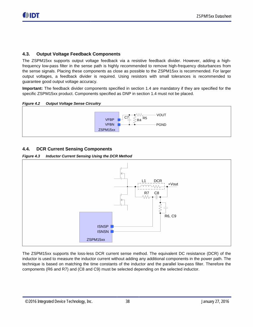
ZSPM15xx Datasheet
© 2016 Integrated Device Technology, Inc. 38 January 27, 2016
4.3. Output Voltage Feedback Components The ZSPM15xx supports output voltage feedback via a resistive feedback divider. However, adding a high-frequency low-pass filter in the sense path is highly recommended to remove high-frequency disturbances from the sense signals. Placing these components as close as possible to the ZSPM15xx is recommended. For larger output voltages, a feedback divider is required. Using resistors with small tolerances is recommended to guarantee good output voltage accuracy. Important: The feedback divider components specified in section 1.4 are mandatory if they are specified for the specific ZSPM15xx product. Components specified as DNP in section 1.4 must not be placed.
Figure 4.2 Output Voltage Sense Circuitry
4.4. DCR Current Sensing Components Figure 4.3 Inductor Current Sensing Using the DCR Method
The ZSPM15xx supports the loss-less DCR current sense method. The equivalent DC resistance (DCR) of the inductor is used to measure the inductor current without adding any additional components in the power path. The technique is based on matching the time constants of the inductor and the parallel low-pass filter. Therefore the components (R6 and R7) and (C8 and C9) must be selected depending on the selected inductor.
VFBPVFBN
R4 R5C7
PGND
VOUT
ZSPM15xx
ZSPM15xx
+Vout
R7
R6, C9
ISNSPISNSN
C8
L1 DCR
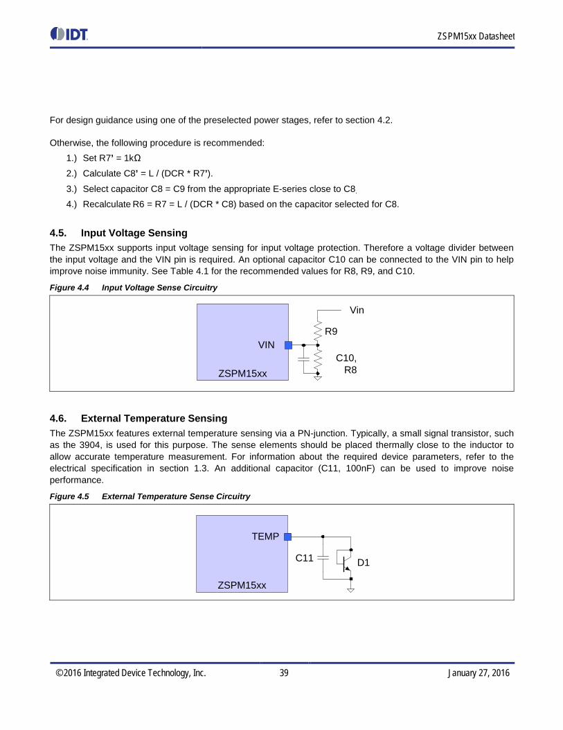
ZSPM15xx Datasheet
© 2016 Integrated Device Technology, Inc. 39 January 27, 2016
For design guidance using one of the preselected power stages, refer to section 4.2.
Otherwise, the following procedure is recommended: 1.) Set R7’ = 1kΩ
2.) Calculate C8’ = L / (DCR * R7’). 3.) Select capacitor C8 = C9 from the appropriate E-series close to C8. 4.) Recalculate R6 = R7 = L / (DCR * C8) based on the capacitor selected for C8.
4.5. Input Voltage Sensing The ZSPM15xx supports input voltage sensing for input voltage protection. Therefore a voltage divider between the input voltage and the VIN pin is required. An optional capacitor C10 can be connected to the VIN pin to help improve noise immunity. See Table 4.1 for the recommended values for R8, R9, and C10.
Figure 4.4 Input Voltage Sense Circuitry
4.6. External Temperature Sensing The ZSPM15xx features external temperature sensing via a PN-junction. Typically, a small signal transistor, such as the 3904, is used for this purpose. The sense elements should be placed thermally close to the inductor to allow accurate temperature measurement. For information about the required device parameters, refer to the electrical specification in section 1.3. An additional capacitor (C11, 100nF) can be used to improve noise performance.
Figure 4.5 External Temperature Sense Circuitry
VIN
Vin
R9
C10, R8ZSPM15xx
TEMP
D1
ZSPM15xx
C11
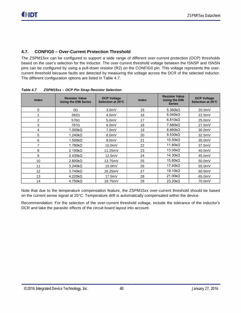
ZSPM15xx Datasheet
© 2016 Integrated Device Technology, Inc. 40 January 27, 2016
4.7. CONFIG0 – Over-Current Protection Threshold The ZSPM15xx can be configured to support a wide range of different over-current protection (OCP) thresholds based on the user’s selection for the inductor. The over-current threshold voltage between the ISNSP and ISNSN pins can be configured by using a pull-down resistor (R2) on the CONFIG0 pin. This voltage represents the over-current threshold because faults are detected by measuring the voltage across the DCR of the selected inductor. The different configuration options are listed in Table 4.7.
Table 4.7 ZSPM15xx – OCP Pin Strap Resistor Selection
Index Resistor Value Using the E96 Series
OCP Voltage Selection at 25°C Index
Resistor Value Using the E96
Series OCP Voltage
Selection at 25°C
0 0Ω 3.0mV 15 5.360kΩ 20.0mV 1 392Ω 4.0mV 16 6.040kΩ 22.5mV 2 576Ω 5.0mV 17 6.810kΩ 25.0mV 3 787Ω 6.0mV 18 7.680kΩ 27.5mV 4 1.000kΩ 7.0mV 19 8.660kΩ 30.0mV 5 1.240kΩ 8.0mV 20 9.530kΩ 32.5mV 6 1.500kΩ 9.0mV 21 10.50kΩ 35.0mV 7 1.780kΩ 10.0mV 22 11.80kΩ 37.5mV 8 2.100kΩ 11.25mV 23 13.00kΩ 40.0mV 9 2.430kΩ 12.5mV 24 14.30kΩ 45.0mV 10 2.800kΩ 13.75mV 25 15.80kΩ 50.0mV 11 3.240kΩ 15.0mV 26 17.40kΩ 55.0mV 12 3.740kΩ 16.25mV 27 19.10kΩ 60.0mV 13 4.220kΩ 17.5mV 28 21.00kΩ 65.0mV 14 4.750kΩ 18.75mV 29 23.20kΩ 70.0mV
Note that due to the temperature compensation feature, the ZSPM15xx over-current threshold should be based on the current sense signal at 25°C. Temperature drift is automatically compensated within the device.
Recommendation: For the selection of the over-current threshold voltage, include the tolerance of the inductor’s DCR and take the parasitic effects of the circuit board layout into account.

ZSPM15xx Datasheet
© 2016 Integrated Device Technology, Inc. 41 January 27, 2016
4.8. CONFIG1 – Compensation Loop and Output Voltage Slew Rate The ZSPM15xx controllers can be configured to operate over a wide range of output capacitance. Four ranges of output capacitance have been specified to match typical customer requirements (see Table 4.8). For each output capacitance range, an optimized compensation loop can be selected. The appropriate compensator should be selected based on the application requirements.
Typical performance measurements for both load transient performance and open-loop Bode plots can be found in section 5.
Note: Using less output capacitance than the minimum capacitance given in Table 4.8 is not recommended.
Table 4.8 Recommended Output Capacitor Ranges
Capacitor Range Ceramic Capacitor Bulk Electrolytic Capacitors Suitable Compensator
#1 Minimum 200µF Maximum 500µF
None Comp0
#2 Minimum 500µF
Maximum 1000µF None
Comp1
#3 Minimum 200µF Maximum 500µF
Minimum 2 x 470µF, 7mΩ ESR Maximum 4 x 470µF, 7mΩ ESR
Comp2
#4 Minimum 500µF
Maximum 1000µF Minimum 4 x 470µF, 7mΩ ESR Maximum 6 x 470µF, 7mΩ ESR
Comp3
To achieve the optimal performance for a given output capacitor range, one of four sets of compensation loop parameters, Comp0 to Comp3, should be selected with a resistor between the CONFIG1 and GND pins. The compensation loop parameters have been configured to ensure optimal transient performance and good control loop stability margins.
For each set of compensation loop parameters, there is a choice of seven slew rates for the output voltage during power-up. The selection of the slew rate can be used to limit the input current of the DC/DC converter while it is ramping up the output voltage. The current needed to charge the output capacitors increases in direct proportion to the slew rate.

ZSPM15xx Datasheet
© 2016 Integrated Device Technology, Inc. 42 January 27, 2016
Table 4.9 gives a complete list of the selectable compensation loop parameters and slew rates together with the equivalent pin-strap resistor values (R3) for the ZSPM1501 to ZSPM1506 and the ZSPM1511 to ZSPM1513. Table 4.10, Table 4.11, and Table 4.12 provide the values and settings for the ZSPM1507, ZSPM1508, and ZSPM1509 respectively.
Table 4.9 Compensator and VOUT Slew Rate Pin Strap Resistor Selection for the ZSPM1501 to ZSPM1506 and the ZSPM1511 to ZSPM1513
Index Resistor
Value Using the E96 Series
Compensator Vout Slew Rate Index
Resistor Value
Using the E96 Series
Compensator Vout Slew Rate
0 0Ω
Comp0 (Capacitor Range #1)
2.700 V/ms 14 4.750kΩ
Comp2 (Capacitor Range #3)
2.700 V/ms
1 392Ω 1.350 V/ms 15 5.360kΩ 1.350 V/ms
2 576Ω 0.675 V/ms 16 6.040kΩ 0.675 V/ms
3 787Ω 0.300 V/ms 17 6.810kΩ 0.300 V/ms
4 1.000kΩ 0.200 V/ms 18 7.680kΩ 0.200 V/ms
5 1.240kΩ 0.150 V/ms 19 8.660kΩ 0.150 V/ms
6 1.500kΩ 0.100 V/ms 20 9.530kΩ 0.100 V/ms
7 1.780kΩ
Comp1 (Capacitor Range #2)
2.700 V/ms 21 10.50kΩ
Comp3 (Capacitor Range #4)
2.700 V/ms
8 2.100kΩ 1.350 V/ms 22 11.80kΩ 1.350 V/ms
9 2.430kΩ 0.675 V/ms 23 13.00kΩ 0.675 V/ms
10 2.800kΩ 0.300 V/ms 24 14.30kΩ 0.300 V/ms
11 3.240kΩ 0.200 V/ms 25 15.80kΩ 0.200 V/ms
12 3.740kΩ 0.150 V/ms 26 17.40kΩ 0.150 V/ms
13 4.220kΩ 0.100 V/ms 27 19.10kΩ 0.100 V/ms

ZSPM15xx Datasheet
© 2016 Integrated Device Technology, Inc. 43 January 27, 2016
Table 4.10 Compensator and VOUT Slew Rate Pin Strap Resistor Selection for the ZSPM1507
Index Resistor
Value Using the E96 Series
Compensator Vout Slew Rate Index
Resistor Value
Using the E96 Series
Compensator Vout Slew Rate
0 0Ω
Comp0 (Capacitor Range #1)
6.756 V/ms 14 4.750kΩ
Comp2 (Capacitor Range #3)
6.756 V/ms
1 392Ω 3.378 V/ms 15 5.360kΩ 3.378 V/ms
2 576Ω 1.689 V/ms 16 6.040kΩ 1.689 V/ms
3 787Ω 0.750 V/ms 17 6.810kΩ 0.750 V/ms
4 1.000kΩ 0.517 V/ms 18 7.680kΩ 0.517 V/ms
5 1.240kΩ 0.374 V/ms 19 8.660kΩ 0.374 V/ms
6 1.500kΩ 0.250 V/ms 20 9.530kΩ 0.250 V/ms
7 1.780kΩ
Comp1 (Capacitor Range #2)
6.756 V/ms 21 10.50kΩ
Comp3 (Capacitor Range #4)
6.756 V/ms
8 2.100kΩ 3.378 V/ms 22 11.80kΩ 3.378 V/ms
9 2.430kΩ 1.689 V/ms 23 13.00kΩ 1.689 V/ms
10 2.800kΩ 0.750 V/ms 24 14.30kΩ 0.750 V/ms
11 3.240kΩ 0.517 V/ms 25 15.80kΩ 0.517 V/ms
12 3.740kΩ 0.374 V/ms 26 17.40kΩ 0.374 V/ms
13 4.220kΩ 0.250 V/ms 27 19.10kΩ 0.250 V/ms

ZSPM15xx Datasheet
© 2016 Integrated Device Technology, Inc. 44 January 27, 2016
Table 4.11 Compensator and VOUT Slew Rate Pin Strap Resistor Selection for the ZSPM1508
Index Resistor
Value Using the E96 Series
Compensator Vout Slew Rate Index
Resistor Value
Using the E96 Series
Compensator Vout Slew Rate
0 0Ω
Comp0 (Capacitor Range #1)
2.896 V/ms 14 4.750kΩ
Comp2 (Capacitor Range #3)
2.896 V/ms
1 392Ω 1.659 V/ms 15 5.360kΩ 1.659 V/ms
2 576Ω 1.051 V/ms 16 6.040kΩ 1.051 V/ms
3 787Ω 0.827 V/ms 17 6.810kΩ 0.827 V/ms
4 1.000kΩ 0.643 V/ms 18 7.680kΩ 0.643 V/ms
5 1.240kΩ 0.428 V/ms 19 8.660kΩ 0.428 V/ms
6 1.500kΩ 0.330 V/ms 20 9.530kΩ 0.330 V/ms
7 1.780kΩ
Comp1 (Capacitor Range #2)
2.896 V/ms 21 10.50kΩ
Comp3 (Capacitor Range #4)
2.896 V/ms
8 2.100kΩ 1.659 V/ms 22 11.80kΩ 1.659 V/ms
9 2.430kΩ 1.051 V/ms 23 13.00kΩ 1.051 V/ms
10 2.800kΩ 0.827 V/ms 24 14.30kΩ 0.827 V/ms
11 3.240kΩ 0.643 V/ms 25 15.80kΩ 0.643 V/ms
12 3.740kΩ 0.428 V/ms 26 17.40kΩ 0.428 V/ms
13 4.220kΩ 0.330 V/ms 27 19.10kΩ 0.330 V/ms
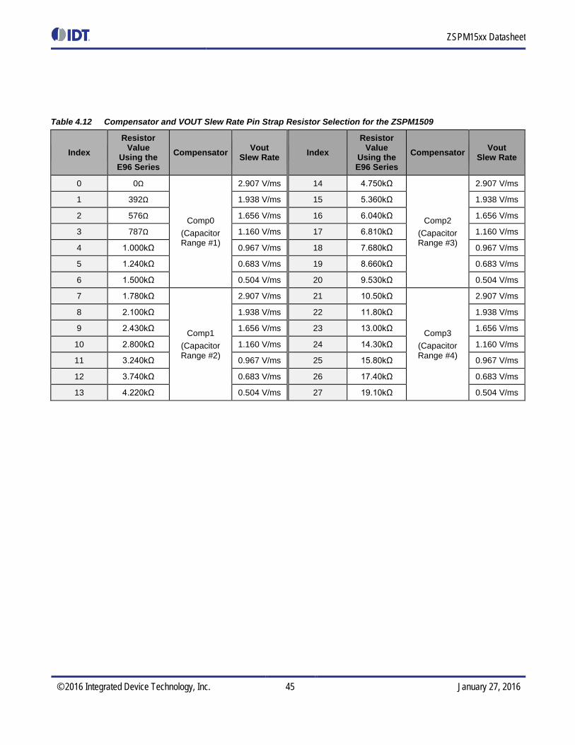
ZSPM15xx Datasheet
© 2016 Integrated Device Technology, Inc. 45 January 27, 2016
Table 4.12 Compensator and VOUT Slew Rate Pin Strap Resistor Selection for the ZSPM1509
Index Resistor
Value Using the E96 Series
Compensator Vout Slew Rate Index
Resistor Value
Using the E96 Series
Compensator Vout Slew Rate
0 0Ω
Comp0 (Capacitor Range #1)
2.907 V/ms 14 4.750kΩ
Comp2 (Capacitor Range #3)
2.907 V/ms
1 392Ω 1.938 V/ms 15 5.360kΩ 1.938 V/ms
2 576Ω 1.656 V/ms 16 6.040kΩ 1.656 V/ms
3 787Ω 1.160 V/ms 17 6.810kΩ 1.160 V/ms
4 1.000kΩ 0.967 V/ms 18 7.680kΩ 0.967 V/ms
5 1.240kΩ 0.683 V/ms 19 8.660kΩ 0.683 V/ms
6 1.500kΩ 0.504 V/ms 20 9.530kΩ 0.504 V/ms
7 1.780kΩ
Comp1 (Capacitor Range #2)
2.907 V/ms 21 10.50kΩ
Comp3 (Capacitor Range #4)
2.907 V/ms
8 2.100kΩ 1.938 V/ms 22 11.80kΩ 1.938 V/ms
9 2.430kΩ 1.656 V/ms 23 13.00kΩ 1.656 V/ms
10 2.800kΩ 1.160 V/ms 24 14.30kΩ 1.160 V/ms
11 3.240kΩ 0.967 V/ms 25 15.80kΩ 0.967 V/ms
12 3.740kΩ 0.683 V/ms 26 17.40kΩ 0.683 V/ms
13 4.220kΩ 0.504 V/ms 27 19.10kΩ 0.504 V/ms

ZSPM15xx Datasheet
© 2016 Integrated Device Technology, Inc. 46 January 27, 2016
5 Typical Performance Data This section gives typical performance data for the individual products in the ZSPM15xx family. The pre-programmed compensation loop parameters for the ZSPM15xx have been designed to ensure stability and optimal transient performance for the specified inductance in combination with one of the four output capacitor ranges (see Table 4.8).
The transient load steps have been generated with a load resistor and a power MOSFET located on the same circuit board as the ZSPM15xx and the recommended reference layout. The Evaluation Kit for the specific ZSPM15xx product can be used to further evaluate the performance of the ZSPM15xx for the four output capacitor ranges.

ZSPM15xx Datasheet
© 2016 Integrated Device Technology, Inc. 47 January 27, 2016
5.1. ZSPM1501 – Typical Load Transient Response – Capacitor Range #1 – Comp0 Test conditions: VIN = 12.0V, VOUT = 0.85V Minimum output capacitance: 2 x 100µF/6.3V X5R Maximum output capacitance: 4 x 100µF/6.3V X5R + 2 x 47µF/10V X7R
Figure 5.1 ZSPM1501 with Comp0; 5A to 15A Load Step; and Min. Capacitance
Figure 5.2 ZSPM1501 with Comp0; 15A to 5A Load Step; and Min. Capacitance
Figure 5.3 ZSPM1501 with Comp0; 5A to 15A Load Step; and Max. Capacitance
Figure 5.4 ZSPM1501 with Comp0; 15A to 5A Load Step; and Max. Capacitance
Figure 5.5 Open Loop Bode Plots for ZSPM1501 with Comp0
-180
-150
-120
-90
-60
-30
0
-40
-30
-20
-10
0
10
20
30
40
1 10 100
Phas
e [d
egre
es]
Gai
n [d
B]
Frequency [kHz]
Max Caps - GainMin Caps - GainMax Caps - PhaseMin Caps - Phase
Ch1 (Blue): VOUT 100mV/div AC Ch2 (Cyan): PWM 5V/div DC Ch4 (Green): Load Trigger 5V/div DC Time Scale: 8µs/div
Ch1 (Blue): VOUT 100mV/div AC Ch2 (Cyan): PWM 5V/div DC Ch4 (Green): Load Trigger 5V/div DC Time Scale: 8µs/div
Ch1: (Blue): VOUT 100mV/div AC Ch2: (Cyan): PWM 5V/div DC Ch4: (Green): Load Trigger 5V/div DC Time Scale: 8µs/div
Ch1: (Blue): VOUT 100mV/div AC Ch2: (Cyan): PWM 5V/div DC Ch4: (Green): Load Trigger 5V/div DC Time Scale: 8µs/div

ZSPM15xx Datasheet
© 2016 Integrated Device Technology, Inc. 48 January 27, 2016
5.2. ZSPM1501 – Typical Load Transient Response – Capacitor Range #2 – Comp1 Test conditions: VIN = 12.0V, VOUT = 0.85V Minimum output capacitance: 5 x 100µF/6.3V X5R Maximum output capacitance: 8 x 100µF/6.3V X5R + 4 x 47µF/10V X7R
Figure 5.6 ZSPM1501 with Comp1; 5A to 15A Load Step; and Min. Capacitance
Figure 5.7 ZSPM1501 with Comp1; 15A to 5A Load Step; and Min. Capacitance
Figure 5.8 ZSPM1501 with Comp1; 5A to 15A Load Step; and Max. Capacitance
Figure 5.9 ZSPM1501 with Comp1; 15A to 5A Load Step; and Max. Capacitance
Figure 5.10 Open Loop Bode Plots for ZSPM1501 with Comp1
-180
-150
-120
-90
-60
-30
0
-40
-30
-20
-10
0
10
20
30
40
1 10 100
Phas
e [d
egre
es]
Gai
n [d
B]
Frequency [kHz]
Max Caps - GainMin Caps - GainMax Caps - PhaseMin Caps - Phase
Ch1 (Blue): VOUT 50mV/div AC Ch2 (Cyan): PWM 5V/div DC Ch4 (Green): Load Trigger 5V/div DC Time Scale: 8µs/div
Ch1 (Blue): VOUT 50mV/div AC Ch2 (Cyan): PWM 5V/div DC Ch4 (Green): Load Trigger 5V/div DC Time Scale: 8µs/div
Ch1 (Blue): VOUT 50mV/div AC Ch2 (Cyan): PWM 5V/div DC Ch4 (Green): Load Trigger 5V/div DC Time Scale: 8µs/div
Ch1 (Blue): VOUT 50mV/div AC Ch2 (Cyan): PWM 5V/div DC Ch4 (Green): Load Trigger 5V/div DC Time Scale: 8µs/div

ZSPM15xx Datasheet
© 2016 Integrated Device Technology, Inc. 49 January 27, 2016
5.3. ZSPM1501 – Typical Load Transient Response – Capacitor Range #3 – Comp2 Test conditions: VIN = 12.0V, VOUT = 0.85V Minimum output capacitance: 2 x 100µF/6.3V X5R + 2x 470µF/7mΩ Maximum output capacitance: 4 x 100µF/6.3V X5R + 2 x 47µF/10V X7R + 4 x 470µF/7mΩ
Figure 5.11 ZSPM1501 with Comp2; 5A to 15A Load Step; and Min. Capacitance
Figure 5.12 ZSPM1501 with Comp2; 15A to 5A Load Step; and Min. Capacitance
Figure 5.13 ZSPM1501 with Comp2; 5A to 15A Load Step; and Max. Capacitance
Figure 5.14 ZSPM1501 with Comp2; 15A to 5A Load Step; and Max. Capacitance
Figure 5.15 Open Loop Bode Plots for ZSPM1501 with Comp2
-180
-150
-120
-90
-60
-30
0
-40
-30
-20
-10
0
10
20
30
40
1 10 100
Phas
e [d
egre
es]
Gai
n [d
B]
Frequency [kHz]
Max Caps - GainMin Caps - GainMax Caps - PhaseMin Caps - Phase
Ch1 (Blue): VOUT 50mV/div AC Ch2 (Cyan): PWM 5V/div DC Ch4 (Green): Load Trigger 5V/div DC Time Scale: 8µs/div
Ch1 (Blue): VOUT 50mV/div AC Ch2 (Cyan): PWM 5V/div DC Ch4 (Green): Load Trigger 5V/div DC Time Scale: 8µs/div
Ch1 (Blue): VOUT 50mV/div AC Ch2 (Cyan): PWM 5V/div DC Ch4 (Green): Load Trigger 5V/div DC Time Scale: 8µs/div
Ch1 (Blue): VOUT 50mV/div AC Ch2 (Cyan): PWM 5V/div DC Ch4 (Green): Load Trigger 5V/div DC Time Scale: 8µs/div

ZSPM15xx Datasheet
© 2016 Integrated Device Technology, Inc. 50 January 27, 2016
5.4. ZSPM1501 – Typical Load Transient Response – Capacitor Range #4 – Comp3 Test conditions: VIN = 12.0V, VOUT = 0.85V Minimum output capacitance: 5 x 100µF/6.3V X5R + 4 x 470µF/7mΩ Maximum output capacitance: 8 x 100µF/6.3V X5R + 4 x 47µF/10V X7R + 6 x 470µF/7mΩ
Figure 5.16 ZSPM1501 with Comp3; 5A to 15A Load Step; and Min. Capacitance
Figure 5.17 ZSPM1501 with Comp3; 15A to 5A Load Step; and Min. Capacitance
Figure 5.18 ZSPM1501 with Comp3; 5A to 15A Load Step; and Max. Capacitance
Figure 5.19 ZSPM1501 with Comp3; 15A to 5A Load Step; and Max. Capacitance
Figure 5.20 Open Loop Bode Plots for ZSPM1501 with Comp3
-180
-150
-120
-90
-60
-30
0
-40
-30
-20
-10
0
10
20
30
40
1 10 100
Phas
e [d
egre
es]
Gai
n [d
B]
Frequency [kHz]
Max Caps - GainMin Caps - GainMax Caps - PhaseMin Caps - Phase
Ch1 (Blue): VOUT 20mV/div AC Ch2 (Cyan): PWM 5V/div DC Ch4 (Green): Load Trigger 5V/div DC Time Scale: 8µs/div
Ch1 (Blue): VOUT 20mV/div AC Ch2 (Cyan): PWM 5V/div DC Ch4 (Green): Load Trigger 5V/div DC Time Scale: 8µs/div
Ch1 (Blue): VOUT 20mV/div AC Ch2 (Cyan): PWM 5V/div DC Ch4 (Green): Load Trigger 5V/div DC Time Scale: 8µs/div
Ch1 (Blue): VOUT 20mV/div AC Ch2 (Cyan): PWM 5V/div DC Ch4 (Green): Load Trigger 5V/div DC Time Scale: 8µs/div
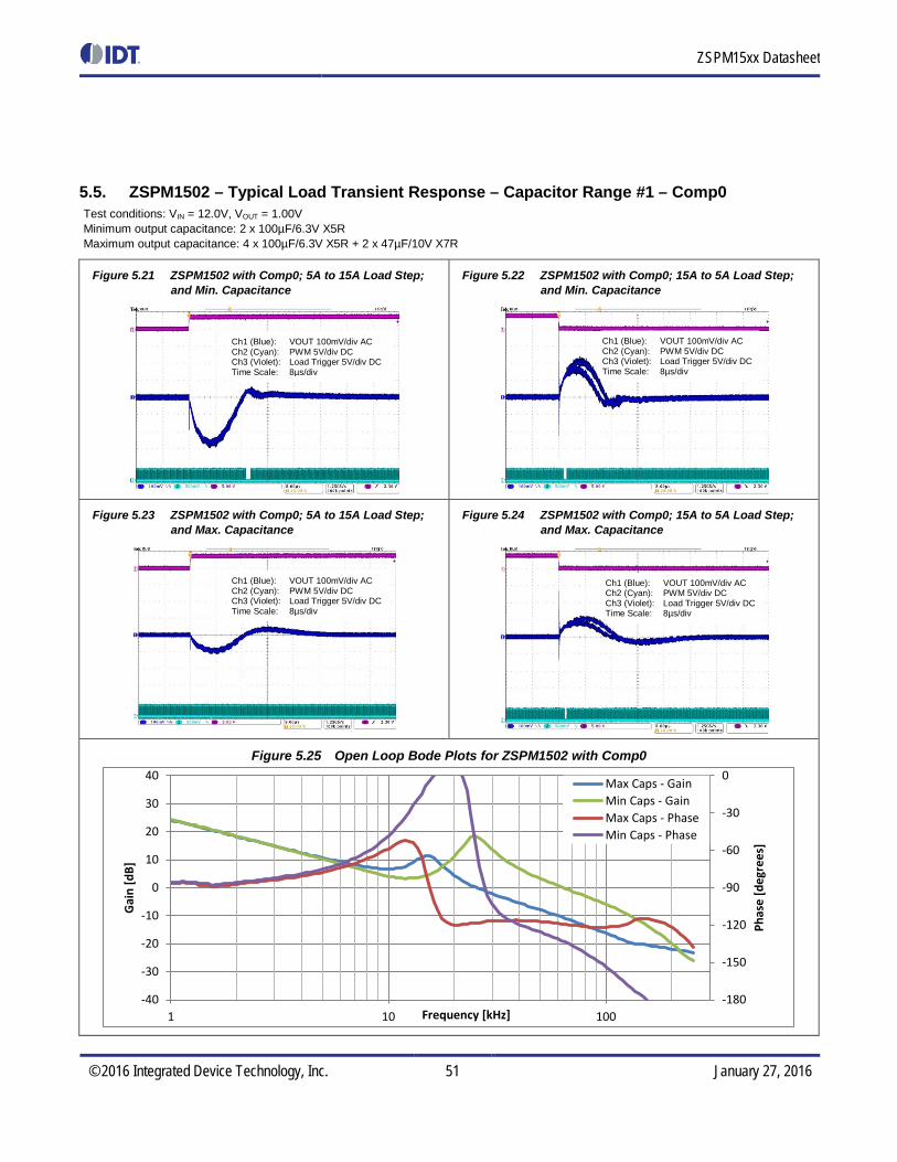
ZSPM15xx Datasheet
© 2016 Integrated Device Technology, Inc. 51 January 27, 2016
5.5. ZSPM1502 – Typical Load Transient Response – Capacitor Range #1 – Comp0 Test conditions: VIN = 12.0V, VOUT = 1.00V Minimum output capacitance: 2 x 100µF/6.3V X5R Maximum output capacitance: 4 x 100µF/6.3V X5R + 2 x 47µF/10V X7R
Figure 5.21 ZSPM1502 with Comp0; 5A to 15A Load Step; and Min. Capacitance
Figure 5.22 ZSPM1502 with Comp0; 15A to 5A Load Step; and Min. Capacitance
Figure 5.23 ZSPM1502 with Comp0; 5A to 15A Load Step; and Max. Capacitance
Figure 5.24 ZSPM1502 with Comp0; 15A to 5A Load Step; and Max. Capacitance
Figure 5.25 Open Loop Bode Plots for ZSPM1502 with Comp0
-180
-150
-120
-90
-60
-30
0
-40
-30
-20
-10
0
10
20
30
40
1 10 100
Phas
e [d
egre
es]
Gai
n [d
B]
Frequency [kHz]
Max Caps - GainMin Caps - GainMax Caps - PhaseMin Caps - Phase
Ch1 (Blue): VOUT 100mV/div AC Ch2 (Cyan): PWM 5V/div DC Ch3 (Violet): Load Trigger 5V/div DC Time Scale: 8µs/div
Ch1 (Blue): VOUT 100mV/div AC Ch2 (Cyan): PWM 5V/div DC Ch3 (Violet): Load Trigger 5V/div DC Time Scale: 8µs/div
Ch1 (Blue): VOUT 100mV/div AC Ch2 (Cyan): PWM 5V/div DC Ch3 (Violet): Load Trigger 5V/div DC Time Scale: 8µs/div
Ch1 (Blue): VOUT 100mV/div AC Ch2 (Cyan): PWM 5V/div DC Ch3 (Violet): Load Trigger 5V/div DC Time Scale: 8µs/div

ZSPM15xx Datasheet
© 2016 Integrated Device Technology, Inc. 52 January 27, 2016
5.6. ZSPM1502 – Typical Load Transient Response – Capacitor Range #2 – Comp1 Test conditions: VIN = 12.0V, VOUT = 1.00V Minimum output capacitance: 5 x 100µF/6.3V X5R Maximum output capacitance: 8 x 100µF/6.3V X5R + 4 x 47µF/10V X7R
Figure 5.26 ZSPM1502 with Comp1; 5A to 15A Load Step; and Min. Capacitance
Figure 5.27 ZSPM1502 with Comp1; 15A to 5A Load Step; and Min. Capacitance
Figure 5.28 ZSPM1502 with Comp1; 5A to 15A Load Step; and Max. Capacitance
Figure 5.29 ZSPM1502 with Comp1; 15A to 5A Load Step; and Max. Capacitance
Figure 5.30 Open Loop Bode Plots for ZSPM1502 with Comp1
-180
-150
-120
-90
-60
-30
0
-40
-30
-20
-10
0
10
20
30
40
1 10 100
Phas
e [d
egre
es]
Gai
n [d
B]
Frequency [kHz]
Max Caps - GainMin Caps - GainMax Caps - PhaseMin Caps - Phase
Ch1 (Blue): VOUT 50mV/div AC Ch2 (Cyan): PWM 5V/div DC Ch3 (Violet): Load Trigger 5V/div DC Time Scale: 8µs/div
Ch1 (Blue): VOUT 50mV/div AC Ch2 (Cyan): PWM 5V/div DC Ch3 (Violet): Load Trigger 5V/div DC Time Scale: 8µs/div
Ch1 (Blue): VOUT 50mV/div AC Ch2 (Cyan): PWM 5V/div DC Ch3 (Violet): Load Trigger 5V/div DC Time Scale: 8µs/div
Ch1 (Blue): VOUT 50mV/div AC Ch2 (Cyan): PWM 5V/div DC Ch3 (Violet): Load Trigger 5V/div DC Time Scale: 8µs/div

ZSPM15xx Datasheet
© 2016 Integrated Device Technology, Inc. 53 January 27, 2016
5.7. ZSPM1502 – Typical Load Transient Response – Capacitor Range #3 – Comp2 Test conditions: VIN = 12.0V, VOUT = 1.00V Minimum output capacitance: 2 x 100µF/6.3V X5R + 2 x 470µF/7mΩ Maximum output capacitance: 4 x 100µF/6.3V X5R + 2 x 47µF/10V X7R + 4 x 470µF/7mΩ
Figure 5.31 ZSPM1502 with Comp2; 5A to 15A Load Step; and Min. Capacitance
Figure 5.32 ZSPM1502 with Comp2; 15A to 5A Load Step; and Min. Capacitance
Figure 5.33 ZSPM1502 with Comp2; 5A to 15A Load Step; and Max. Capacitance
Figure 5.34 ZSPM1502 with Comp2; 15A to 5A Load Step; and Max. Capacitance
Figure 5.35 Open Loop Bode Plots for ZSPM1502 with Comp2
-180
-150
-120
-90
-60
-30
0
-40
-30
-20
-10
0
10
20
30
40
1 10 100
Phas
e [d
egre
es]
Gai
n [d
B]
Frequency [kHz]
Max Caps - GainMin Caps - GainMax Caps - PhaseMin Caps - Phase
Ch1 (Blue): VOUT 50mV/div AC Ch2 (Cyan): PWM 5V/div DC Ch3 (Violet): Load Trigger 5V/div DC Time Scale: 8µs/div
Ch1 (Blue): VOUT 50mV/div AC Ch2 (Cyan): PWM 5V/div DC Ch3 (Violet): Load Trigger 5V/div DC Time Scale: 8µs/div
Ch1 (Blue): VOUT 50mV/div AC Ch2 (Cyan): PWM 5V/div DC Ch3 (Violet): Load Trigger 5V/div DC Time Scale: 8µs/div
Ch1 (Blue): VOUT 50mV/div AC Ch2 (Cyan): PWM 5V/div DC Ch3 (Violet): Load Trigger 5V/div DC Time Scale: 8µs/div

ZSPM15xx Datasheet
© 2016 Integrated Device Technology, Inc. 54 January 27, 2016
5.8. ZSPM1502 – Typical Load Transient Response – Capacitor Range #4 – Comp3 Test conditions: VIN = 12.0V, VOUT = 1.00V Minimum output capacitance: 5 x 100µF/6.3V X5R + 4 x 470µF/7mΩ Maximum output capacitance: 8 x 100µF/6.3V X5R + 4 x 47µF/10V X7R + 6 x 470µF/7mΩ
Figure 5.36 ZSPM1502 with Comp3; 5A to 15A Load Step; and Min. Capacitance
Figure 5.37 ZSPM1502 with Comp3; 15A to 5A Load Step; and Min. Capacitance
Figure 5.38 ZSPM1502 with Comp3; 5A to 15A Load Step; and Max. Capacitance
Figure 5.39 ZSPM1502 with Comp3; 15A to 5A Load Step; and Max. Capacitance
Figure 5.40 Open Loop Bode Plots for ZSPM1502 with Comp3
-180
-150
-120
-90
-60
-30
0
-40
-30
-20
-10
0
10
20
30
40
1 10 100
Phas
e [d
egre
es]
Gai
n [d
B]
Frequency [kHz]
Max Caps - GainMin Caps - GainMax Caps - PhaseMin Caps - Phase
Ch1 (Blue): VOUT 20mV/div AC Ch2 (Cyan): PWM 5V/div DC Ch3 (Violet): Load Trigger 5V/div DC Time Scale: 8µs/div
Ch1 (Blue): VOUT 20mV/div AC Ch2 (Cyan): PWM 5V/div DC Ch3 (Violet): Load Trigger 5V/div DC Time Scale: 8µs/div
Ch1 (Blue): VOUT 20mV/div AC Ch2 (Cyan): PWM 5V/div DC Ch3 (Violet): Load Trigger 5V/div DC Time Scale: 8µs/div
Ch1 (Blue): VOUT 20mV/div AC Ch2 (Cyan): PWM 5V/div DC Ch3 (Violet): Load Trigger 5V/div DC Time Scale: 8µs/div
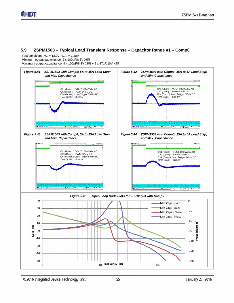
ZSPM15xx Datasheet
© 2016 Integrated Device Technology, Inc. 55 January 27, 2016
5.9. ZSPM1503 – Typical Load Transient Response – Capacitor Range #1 – Comp0 Test conditions: VIN = 12.0V, VOUT = 1.20V Minimum output capacitance: 2 x 100µF/6.3V X5R Maximum output capacitance: 4 x 100µF/6.3V X5R + 2 x 47µF/10V X7R
Figure 5.41 ZSPM1503 with Comp0; 5A to 15A Load Step; and Min. Capacitance
Figure 5.42 ZSPM1503 with Comp0; 15A to 5A Load Step; and Min. Capacitance
Figure 5.43 ZSPM1503 with Comp0; 5A to 15A Load Step; and Max. Capacitance
Figure 5.44 ZSPM1503 with Comp0; 15A to 5A Load Step; and Max. Capacitance
Figure 5.45 Open Loop Bode Plots for ZSPM1503 with Comp0
-180
-150
-120
-90
-60
-30
0
-40
-30
-20
-10
0
10
20
30
40
1 10 100
Phas
e [d
egre
es]
Gai
n [d
B]
Frequency [kHz]
Max Caps - GainMin Caps - GainMax Caps - PhaseMin Caps - Phase
Ch1 (Blue): VOUT 100mV/div AC Ch2 (Cyan): PWM 5V/div DC Ch4 (Green): Load Trigger 5V/div DC Time Scale: 8µs/div
Ch1 (Blue): VOUT 100mV/div AC Ch2 (Cyan): PWM 5V/div DC Ch4 (Green): Load Trigger 5V/div DC Time Scale: 8µs/div
Ch1 (Blue): VOUT 100mV/div AC Ch2 (Cyan): PWM 5V/div DC Ch4 (Green): Load Trigger 5V/div DC Time Scale: 8µs/div
Ch1 (Blue): VOUT 100mV/div AC Ch2 (Cyan): PWM 5V/div DC Ch4 (Green): Load Trigger 5V/div DC Time Scale: 8µs/div
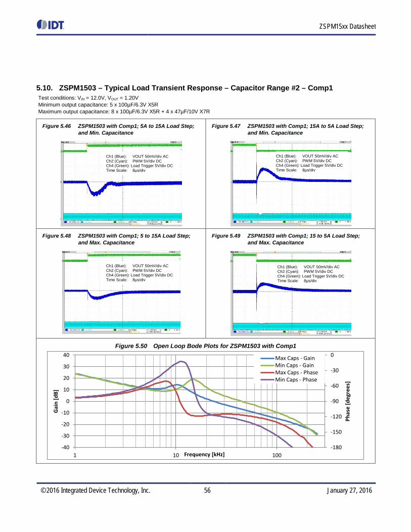
ZSPM15xx Datasheet
© 2016 Integrated Device Technology, Inc. 56 January 27, 2016
5.10. ZSPM1503 – Typical Load Transient Response – Capacitor Range #2 – Comp1 Test conditions: VIN = 12.0V, VOUT = 1.20V Minimum output capacitance: 5 x 100µF/6.3V X5R Maximum output capacitance: 8 x 100µF/6.3V X5R + 4 x 47µF/10V X7R
Figure 5.46 ZSPM1503 with Comp1; 5A to 15A Load Step; and Min. Capacitance
Figure 5.47 ZSPM1503 with Comp1; 15A to 5A Load Step; and Min. Capacitance
Figure 5.48 ZSPM1503 with Comp1; 5 to 15A Load Step; and Max. Capacitance
Figure 5.49 ZSPM1503 with Comp1; 15 to 5A Load Step; and Max. Capacitance
Figure 5.50 Open Loop Bode Plots for ZSPM1503 with Comp1
-180
-150
-120
-90
-60
-30
0
-40
-30
-20
-10
0
10
20
30
40
1 10 100
Phas
e [d
egre
es]
Gai
n [d
B]
Frequency [kHz]
Max Caps - GainMin Caps - GainMax Caps - PhaseMin Caps - Phase
Ch1 (Blue): VOUT 50mV/div AC Ch2 (Cyan): PWM 5V/div DC Ch4 (Green): Load Trigger 5V/div DC Time Scale: 8µs/div
Ch1 (Blue): VOUT 50mV/div AC Ch2 (Cyan): PWM 5V/div DC Ch4 (Green): Load Trigger 5V/div DC Time Scale: 8µs/div
Ch1 (Blue): VOUT 50mV/div AC Ch2 (Cyan): PWM 5V/div DC Ch4 (Green): Load Trigger 5V/div DC Time Scale: 8µs/div
Ch1 (Blue): VOUT 50mV/div AC Ch2 (Cyan): PWM 5V/div DC Ch4 (Green): Load Trigger 5V/div DC Time Scale: 8µs/div

ZSPM15xx Datasheet
© 2016 Integrated Device Technology, Inc. 57 January 27, 2016
5.11. ZSPM1503 – Typical Load Transient Response – Capacitor Range #3 – Comp2 Test conditions: VIN = 12.0V, VOUT = 1.20V Minimum output capacitance: 2 x 100µF/6.3V X5R + 2 x 470µF/7mΩ Maximum output capacitance: 4 x 100µF/6.3V X5R + 2 x 47µF/10V X7R + 4 x 470µF/7mΩ
Figure 5.51 ZSPM1503 with Comp2; 5A to 15A Load Step; and Min. Capacitance
Figure 5.52 ZSPM1503 with Comp2; 15A to 5A Load Step; and Min. Capacitance
Figure 5.53 ZSPM1503 with Comp2; 5A to 15A Load Step; and Max. Capacitance
Figure 5.54 ZSPM1503 with Comp2; 15A to 5A Load Step; and Max. Capacitance
Figure 5.55 Open Loop Bode Plots for ZSPM1503 with Comp2
-180
-150
-120
-90
-60
-30
0
-40
-30
-20
-10
0
10
20
30
40
1 10 100
Phas
e [d
egre
es]
Gai
n [d
B]
Frequency [kHz]
Max Caps - GainMin Caps - GainMax Caps - PhaseMin Caps - Phase
Ch1 (Blue): VOUT 50mV/div AC Ch2 (Cyan): PWM 5V/div DC Ch4 (Green): Load Trigger 5V/div DC Time Scale: 8µs/div
Ch1 (Blue): VOUT 50mV/div AC Ch2 (Cyan): PWM 5V/div DC Ch4 (Green): Load Trigger 5V/div DC Time Scale: 8µs/div
Ch1 (Blue): VOUT 50mV/div AC Ch2 (Cyan): PWM 5V/div DC Ch4 (Green): Load Trigger 5V/div DC Time Scale: 8µs/div
Ch1 (Blue): VOUT 50mV/div AC Ch2 (Cyan): PWM 5V/div DC Ch4 (Green): Load Trigger 5V/div DC Time Scale: 8µs/div

ZSPM15xx Datasheet
© 2016 Integrated Device Technology, Inc. 58 January 27, 2016
5.12. ZSPM1503 – Typical Load Transient Response – Capacitor Range #4 – Comp3 Test conditions: VIN = 12.0V, VOUT = 1.20V Minimum output capacitance: 5 x 100µF/6.3V X5R + 4 x 470µF/7mΩ Maximum output capacitance: 8 x 100µF/6.3V X5R + 4 x 47µF/10V X7R + 6 x 470µF/7mΩ
Figure 5.56 ZSPM1503 with Comp3; 5A to 15A Load Step; and Min. Capacitance
Figure 5.57 ZSPM1503 with Comp3; 15A to 5A Load Step; and Min. Capacitance
Figure 5.58 ZSPM1503 with Comp3; 5A to 15A Load Step; and Max. Capacitance
Figure 5.59 ZSPM1503 with Comp3; 15A to 5A Load Step; and Max. Capacitance
Figure 5.60 Open Loop Bode Plots for ZSPM1503 with Comp3
-180
-150
-120
-90
-60
-30
0
-40
-30
-20
-10
0
10
20
30
40
1 10 100
Phas
e [d
egre
es]
Gai
n [d
B]
Frequency [kHz]
Max Caps - GainMin Caps - GainMax Caps - PhaseMin Caps - Phase
Ch1 (Blue): VOUT 20mV/div AC Ch2 (Cyan): PWM 5V/div DC Ch4 (Green): Load Trigger 5V/div DC Time Scale: 8µs/div
Ch1 (Blue): VOUT 20mV/div AC Ch2 (Cyan): PWM 5V/div DC Ch4 (Green): Load Trigger 5V/div DC Time Scale: 8µs/div
Ch1 (Blue): VOUT 20mV/div AC Ch2 (Cyan): PWM 5V/div DC Ch4 (Green): Load Trigger 5V/div DC Time Scale: 8µs/div
Ch1 (Blue): VOUT 20mV/div AC Ch2 (Cyan): PWM 5V/div DC Ch4 (Green): Load Trigger 5V/div DC Time Scale: 8µs/div

ZSPM15xx Datasheet
© 2016 Integrated Device Technology, Inc. 59 January 27, 2016
5.13. ZSPM1504 – Typical Load Transient Response – Capacitor Range #1 – Comp0 Test conditions: VIN = 12.0V, VOUT = 1.50V Minimum output capacitance: 2 x 100µF/6.3V X5R Maximum output capacitance: 4 x 100µF/6.3V X5R + 2 x 47µF/10V X7R
Figure 5.61 ZSPM1504 with Comp0; 5A to 15A Load Step; and Min. Capacitance
Figure 5.62 ZSPM1504 with Comp0; 15A to 5A Load Step; and Min. Capacitance
Figure 5.63 ZSPM1504 with Comp0; 5A to 15A Load Step; and Max. Capacitance
Figure 5.64 ZSPM1504 with Comp0; 15A to 5A Load Step; and Max. Capacitance
Figure 5.65 Open Loop Bode Plots for ZSPM1504 with Comp0
-180
-150
-120
-90
-60
-30
0
-40
-30
-20
-10
0
10
20
30
40
1 10 100
Phas
e [d
egre
es]
Gai
n [d
B]
Frequency [kHz]
Max Caps - Gain
Min Caps - Gain
Max Caps - Phase
Min Caps - Phase
Ch1 (Blue): VOUT 100mV/div AC Ch2 (Cyan): PWM 5V/div DC Ch3 (Violet): Load Trigger 5V/div DC Time Scale: 10µs/div
Ch1 (Blue): VOUT 100mV/div AC Ch2 (Cyan): PWM 5V/div DC Ch3 (Violet): Load Trigger 5V/div DC Time Scale: 10µs/div
Ch1 (Blue): VOUT 100mV/div AC Ch2 (Cyan): PWM 5V/div DC Ch3 (Violet): Load Trigger 5V/div DC Time Scale: 10µs/div
Ch1 (Blue): VOUT 100mV/div AC Ch2 (Cyan): PWM 5V/div DC Ch3 (Violet): Load Trigger 5V/div DC Time Scale: 10µs/div

ZSPM15xx Datasheet
© 2016 Integrated Device Technology, Inc. 60 January 27, 2016
5.14. ZSPM1504 – Typical Load Transient Response – Capacitor Range #2 – Comp1 Test conditions: VIN = 12.0V, VOUT = 1.50V Minimum output capacitance: 5 x 100µF/6.3V X5R Maximum output capacitance: 8 x 100µF/6.3V X5R + 4 x 47µF/10V X7R
Figure 5.66 ZSPM1504 with Comp1; 5A to 15A Load Step; and Min. Capacitance
Figure 5.67 ZSPM1504 with Comp1; 15A to 5A Load Step; and Min. Capacitance
Figure 5.68 ZSPM1504 with Comp1; 5A to 15A Load Step; and Max. Capacitance
Figure 5.69 ZSPM1504 with Comp1; 15A to 5A Load Step; and Max. Capacitance
Figure 5.70 Open Loop Bode Plots for ZSPM1504 with Comp1
-180
-150
-120
-90
-60
-30
0
-40
-30
-20
-10
0
10
20
30
40
1 10 100
Phas
e [d
egre
es]
Gai
n [d
B]
Frequency [kHz]
Max Caps - GainMin Caps - GainMax Caps - PhaseMin Caps - Phase
Ch1 (Blue): VOUT 50mV/div AC Ch2 (Cyan): PWM 5V/div DC Ch3 (Violet): Load Trigger 5V/div DC Time Scale: 10µs/div
Ch1 (Blue): VOUT 50mV/div AC Ch2 (Cyan): PWM 5V/div DC Ch3 (Violet): Load Trigger 5V/div DC Time Scale: 10µs/div
Ch1 (Blue): VOUT 50mV/div AC Ch2 (Cyan): PWM 5V/div DC Ch3 (Violet): Load Trigger 5V/div DC Time Scale: 10µs/div
Ch1 (Blue): VOUT 50mV/div AC Ch2 (Cyan): PWM 5V/div DC Ch3 (Violet): Load Trigger 5V/div DC Time Scale: 10µs/div
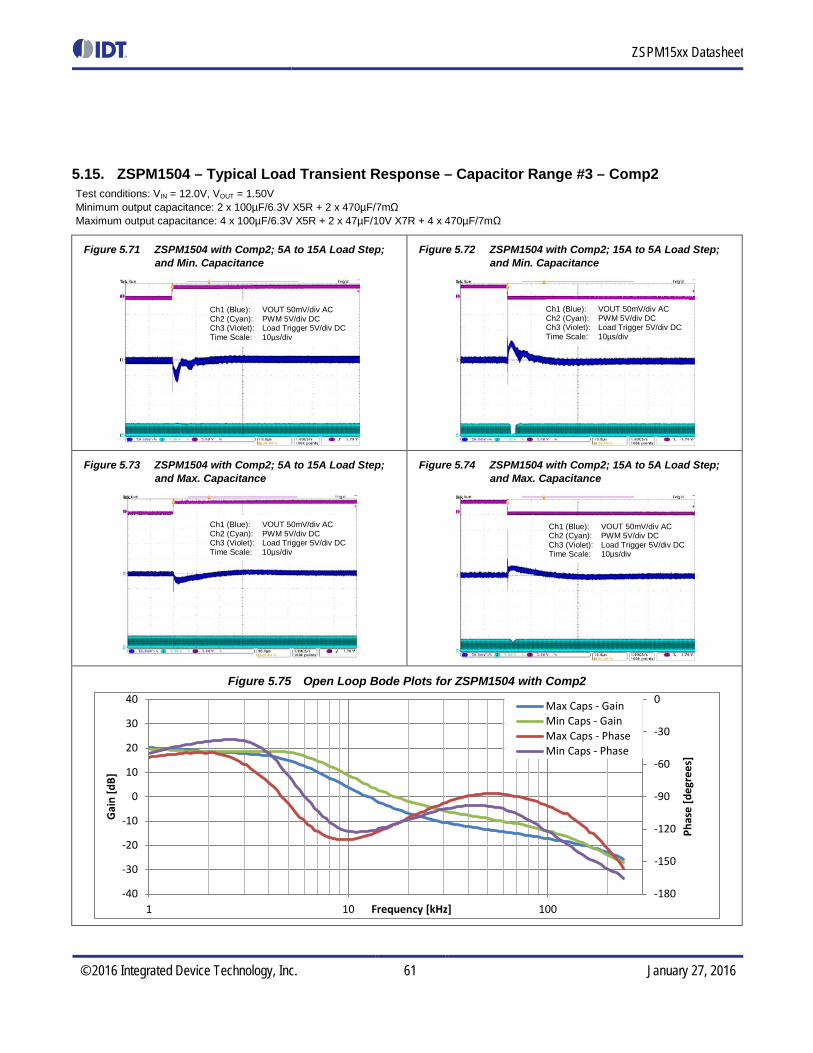
ZSPM15xx Datasheet
© 2016 Integrated Device Technology, Inc. 61 January 27, 2016
5.15. ZSPM1504 – Typical Load Transient Response – Capacitor Range #3 – Comp2 Test conditions: VIN = 12.0V, VOUT = 1.50V Minimum output capacitance: 2 x 100µF/6.3V X5R + 2 x 470µF/7mΩ Maximum output capacitance: 4 x 100µF/6.3V X5R + 2 x 47µF/10V X7R + 4 x 470µF/7mΩ
Figure 5.71 ZSPM1504 with Comp2; 5A to 15A Load Step; and Min. Capacitance
Figure 5.72 ZSPM1504 with Comp2; 15A to 5A Load Step; and Min. Capacitance
Figure 5.73 ZSPM1504 with Comp2; 5A to 15A Load Step; and Max. Capacitance
Figure 5.74 ZSPM1504 with Comp2; 15A to 5A Load Step; and Max. Capacitance
Figure 5.75 Open Loop Bode Plots for ZSPM1504 with Comp2
-180
-150
-120
-90
-60
-30
0
-40
-30
-20
-10
0
10
20
30
40
1 10 100
Phas
e [d
egre
es]
Gai
n [d
B]
Frequency [kHz]
Max Caps - GainMin Caps - GainMax Caps - PhaseMin Caps - Phase
Ch1 (Blue): VOUT 50mV/div AC Ch2 (Cyan): PWM 5V/div DC Ch3 (Violet): Load Trigger 5V/div DC Time Scale: 10µs/div
Ch1 (Blue): VOUT 50mV/div AC Ch2 (Cyan): PWM 5V/div DC Ch3 (Violet): Load Trigger 5V/div DC Time Scale: 10µs/div
Ch1 (Blue): VOUT 50mV/div AC Ch2 (Cyan): PWM 5V/div DC Ch3 (Violet): Load Trigger 5V/div DC Time Scale: 10µs/div
Ch1 (Blue): VOUT 50mV/div AC Ch2 (Cyan): PWM 5V/div DC Ch3 (Violet): Load Trigger 5V/div DC Time Scale: 10µs/div

ZSPM15xx Datasheet
© 2016 Integrated Device Technology, Inc. 62 January 27, 2016
5.16. ZSPM1504 – Typical Load Transient Response – Capacitor Range #4 – Comp3 Test conditions: VIN = 12.0V, VOUT = 1.50V Minimum output capacitance: 5 x 100µF/6.3V X5R + 4 x 470µF/7mΩ Maximum output capacitance: 8 x 100µF/6.3V X5R + 4 x 47µF/10V X7R + 6 x 470µF/7mΩ
Figure 5.76 ZSPM1504 with Comp3; 5A to 15A Load Step; and Min. Capacitance
Figure 5.77 ZSPM1504 with Comp3; 15A to 5A Load Step; and Min. Capacitance
Figure 5.78 ZSPM1504 with Comp3; 5A to 15A Load Step; and Max. Capacitance
Figure 5.79 ZSPM1504 with Comp3; 15A to 5A Load Step; and Max. Capacitance
Figure 5.80 Open Loop Bode Plots for ZSPM1504 with Comp3
-180
-150
-120
-90
-60
-30
0
-40
-30
-20
-10
0
10
20
30
40
1 10 100
Phas
e [d
egre
es]
Gai
n [d
B]
Frequency [kHz]
Max Caps - GainMin Caps - GainMax Caps - PhaseMin Caps - Phase
Ch1 (Blue): VOUT 20mV/div AC Ch2 (Cyan): PWM 5V/div DC Ch3 (Violet): Load Trigger 5V/div DC Time Scale: 10µs/div
Ch1 (Blue): VOUT 20mV/div AC Ch2 (Cyan): PWM 5V/div DC Ch3 (Violet): Load Trigger 5V/div DC Time Scale: 10µs/div
Ch1 (Blue): VOUT 20mV/div AC Ch2 (Cyan): PWM 5V/div DC Ch3 (Violet): Load Trigger 5V/div DC Time Scale: 10µs/div
Ch1 (Blue): VOUT 20mV/div AC Ch2 (Cyan): PWM 5V/div DC Ch3 (Violet): Load Trigger 5V/div DC Time Scale: 10µs/div

ZSPM15xx Datasheet
© 2016 Integrated Device Technology, Inc. 63 January 27, 2016
5.17. ZSPM1505 – Typical Load Transient Response – Capacitor Range #1 – Comp0 Test conditions: VIN = 12.0V, VOUT = 1.80V Minimum output capacitance: 2 x 100µF/6.3V X5R Maximum output capacitance: 4 x 100µF/6.3V X5R + 2 x 47µF/10V X7R
Figure 5.81 ZSPM1505 with Comp0; 5A to 15A Load Step; and Min. Capacitance
Figure 5.82 ZSPM1505 with Comp0; 15A to 5A Load Step; and Min. Capacitance
Figure 5.83 ZSPM1505 with Comp0; 5A to 15A Load Step; and Max. Capacitance
Figure 5.84 ZSPM1505 with Comp0; 15A to 5A Load Step; and Max. Capacitance
Figure 5.85 Open Loop Bode Plots for ZSPM1505 with Comp0
-180
-150
-120
-90
-60
-30
0
-40
-30
-20
-10
0
10
20
30
40
1 10 100
Phas
e [d
egre
es]
Gai
n [d
B]
Frequency [kHz]
Max Caps - GainMin Caps - GainMax Caps - PhaseMin Caps - Phase
Ch1 (Blue): VOUT 100mV/div AC Ch2 (Cyan): PWM 5V/div DC Ch3 (Violet): Load Trigger 5V/div DC Time Scale: 10µs/div
Ch1 (Blue): VOUT 100mV/div AC Ch2 (Cyan): PWM 5V/div DC Ch3 (Violet): Load Trigger 5V/div DC Time Scale: 10µs/div
Ch1 (Blue): VOUT 100mV/div AC Ch2 (Cyan): PWM 5V/div DC Ch3 (Violet): Load Trigger 5V/div DC Time Scale: 10µs/div
Ch1 (Blue): VOUT 100mV/div AC Ch2 (Cyan): PWM 5V/div DC Ch3 (Violet): Load Trigger 5V/div DC Time Scale: 10µs/div
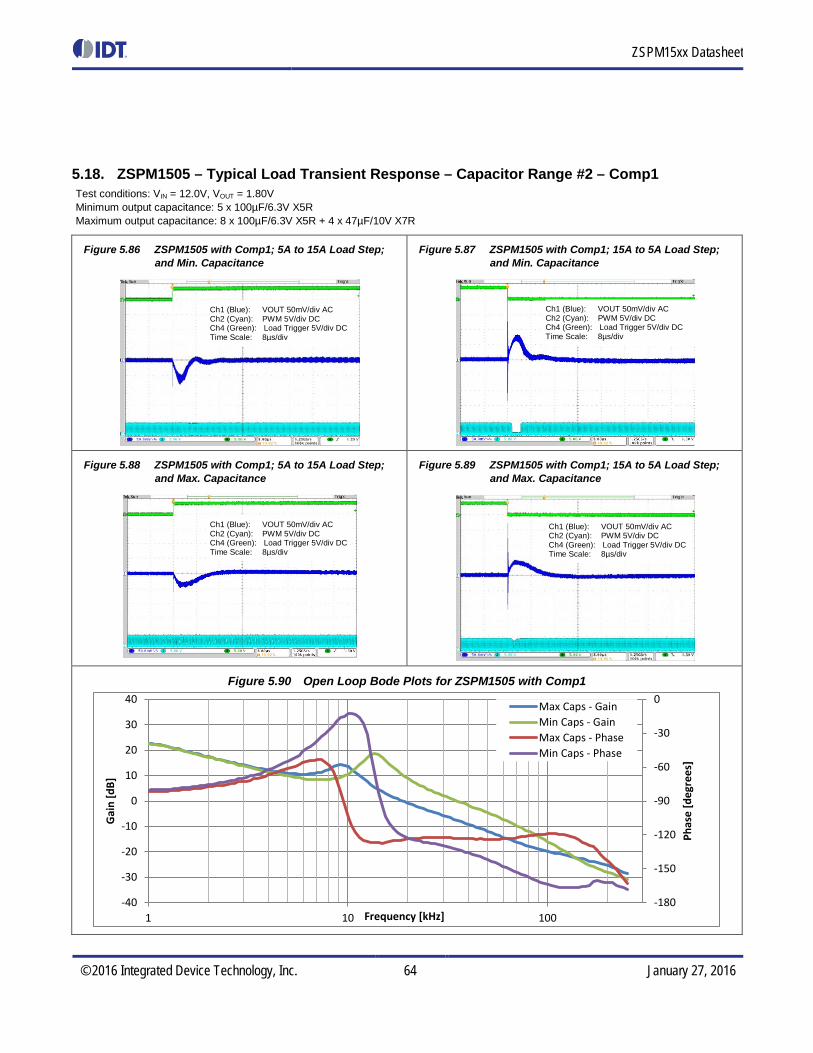
ZSPM15xx Datasheet
© 2016 Integrated Device Technology, Inc. 64 January 27, 2016
5.18. ZSPM1505 – Typical Load Transient Response – Capacitor Range #2 – Comp1 Test conditions: VIN = 12.0V, VOUT = 1.80V Minimum output capacitance: 5 x 100µF/6.3V X5R Maximum output capacitance: 8 x 100µF/6.3V X5R + 4 x 47µF/10V X7R
Figure 5.86 ZSPM1505 with Comp1; 5A to 15A Load Step; and Min. Capacitance
Figure 5.87 ZSPM1505 with Comp1; 15A to 5A Load Step; and Min. Capacitance
Figure 5.88 ZSPM1505 with Comp1; 5A to 15A Load Step; and Max. Capacitance
Figure 5.89 ZSPM1505 with Comp1; 15A to 5A Load Step; and Max. Capacitance
Figure 5.90 Open Loop Bode Plots for ZSPM1505 with Comp1
-180
-150
-120
-90
-60
-30
0
-40
-30
-20
-10
0
10
20
30
40
1 10 100
Phas
e [d
egre
es]
Gai
n [d
B]
Frequency [kHz]
Max Caps - GainMin Caps - GainMax Caps - PhaseMin Caps - Phase
Ch1 (Blue): VOUT 50mV/div AC Ch2 (Cyan): PWM 5V/div DC Ch4 (Green): Load Trigger 5V/div DC Time Scale: 8µs/div
Ch1 (Blue): VOUT 50mV/div AC Ch2 (Cyan): PWM 5V/div DC Ch4 (Green): Load Trigger 5V/div DC Time Scale: 8µs/div
Ch1 (Blue): VOUT 50mV/div AC Ch2 (Cyan): PWM 5V/div DC Ch4 (Green): Load Trigger 5V/div DC Time Scale: 8µs/div
Ch1 (Blue): VOUT 50mV/div AC Ch2 (Cyan): PWM 5V/div DC Ch4 (Green): Load Trigger 5V/div DC Time Scale: 8µs/div
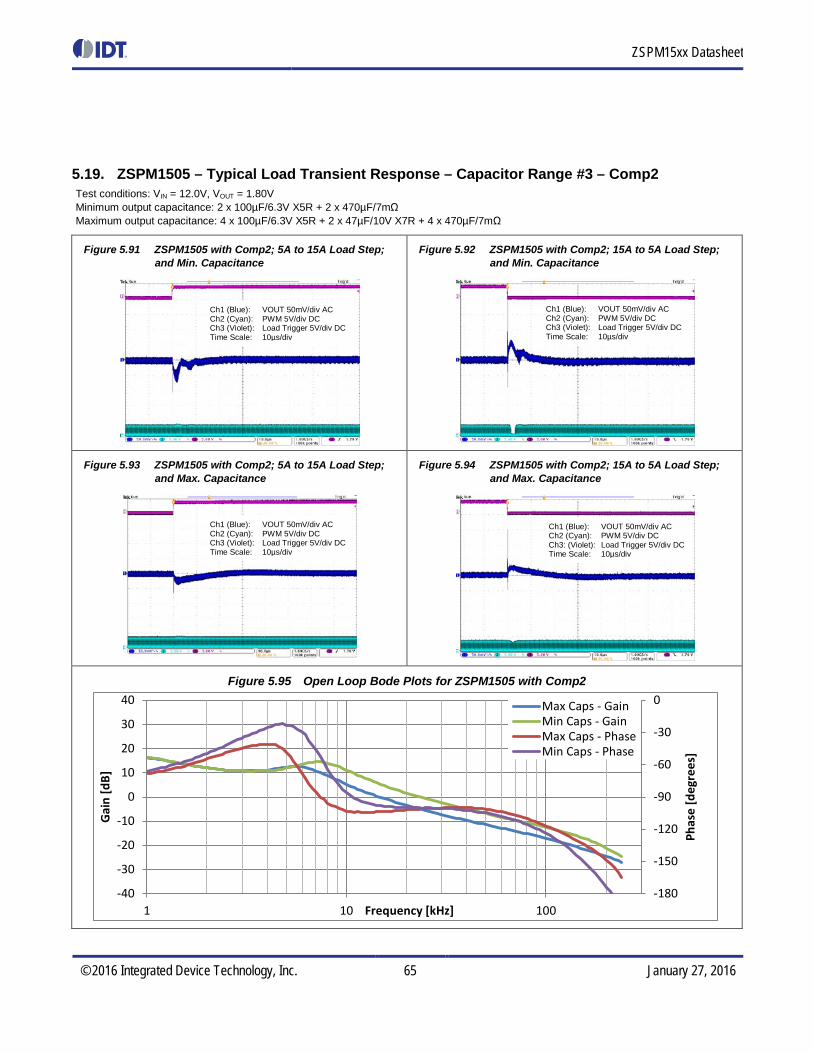
ZSPM15xx Datasheet
© 2016 Integrated Device Technology, Inc. 65 January 27, 2016
5.19. ZSPM1505 – Typical Load Transient Response – Capacitor Range #3 – Comp2 Test conditions: VIN = 12.0V, VOUT = 1.80V Minimum output capacitance: 2 x 100µF/6.3V X5R + 2 x 470µF/7mΩ Maximum output capacitance: 4 x 100µF/6.3V X5R + 2 x 47µF/10V X7R + 4 x 470µF/7mΩ
Figure 5.91 ZSPM1505 with Comp2; 5A to 15A Load Step; and Min. Capacitance
Figure 5.92 ZSPM1505 with Comp2; 15A to 5A Load Step; and Min. Capacitance
Figure 5.93 ZSPM1505 with Comp2; 5A to 15A Load Step; and Max. Capacitance
Figure 5.94 ZSPM1505 with Comp2; 15A to 5A Load Step; and Max. Capacitance
Figure 5.95 Open Loop Bode Plots for ZSPM1505 with Comp2
-180
-150
-120
-90
-60
-30
0
-40
-30
-20
-10
0
10
20
30
40
1 10 100
Phas
e [d
egre
es]
Gai
n [d
B]
Frequency [kHz]
Max Caps - GainMin Caps - GainMax Caps - PhaseMin Caps - Phase
Ch1 (Blue): VOUT 50mV/div AC Ch2 (Cyan): PWM 5V/div DC Ch3 (Violet): Load Trigger 5V/div DC Time Scale: 10µs/div
Ch1 (Blue): VOUT 50mV/div AC Ch2 (Cyan): PWM 5V/div DC Ch3 (Violet): Load Trigger 5V/div DC Time Scale: 10µs/div
Ch1 (Blue): VOUT 50mV/div AC Ch2 (Cyan): PWM 5V/div DC Ch3 (Violet): Load Trigger 5V/div DC Time Scale: 10µs/div
Ch1 (Blue): VOUT 50mV/div AC Ch2 (Cyan): PWM 5V/div DC Ch3: (Violet): Load Trigger 5V/div DC Time Scale: 10µs/div
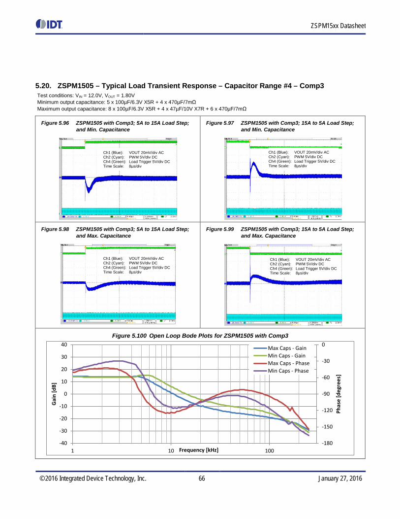
ZSPM15xx Datasheet
© 2016 Integrated Device Technology, Inc. 66 January 27, 2016
5.20. ZSPM1505 – Typical Load Transient Response – Capacitor Range #4 – Comp3 Test conditions: VIN = 12.0V, VOUT = 1.80V Minimum output capacitance: 5 x 100µF/6.3V X5R + 4 x 470µF/7mΩ Maximum output capacitance: 8 x 100µF/6.3V X5R + 4 x 47µF/10V X7R + 6 x 470µF/7mΩ
Figure 5.96 ZSPM1505 with Comp3; 5A to 15A Load Step; and Min. Capacitance
Figure 5.97 ZSPM1505 with Comp3; 15A to 5A Load Step; and Min. Capacitance
Figure 5.98 ZSPM1505 with Comp3; 5A to 15A Load Step; and Max. Capacitance
Figure 5.99 ZSPM1505 with Comp3; 15A to 5A Load Step; and Max. Capacitance
Figure 5.100 Open Loop Bode Plots for ZSPM1505 with Comp3
-180
-150
-120
-90
-60
-30
0
-40
-30
-20
-10
0
10
20
30
40
1 10 100
Phas
e [d
egre
es]
Gai
n [d
B]
Frequency [kHz]
Max Caps - GainMin Caps - GainMax Caps - PhaseMin Caps - Phase
Ch1 (Blue): VOUT 20mV/div AC Ch2 (Cyan): PWM 5V/div DC Ch4 (Green): Load Trigger 5V/div DC Time Scale: 8µs/div
Ch1 (Blue): VOUT 20mV/div AC Ch2 (Cyan): PWM 5V/div DC Ch4 (Green): Load Trigger 5V/div DC Time Scale: 8µs/div
Ch1 (Blue): VOUT 20mV/div AC Ch2 (Cyan): PWM 5V/div DC Ch4 (Green): Load Trigger 5V/div DC Time Scale: 8µs/div
Ch1 (Blue): VOUT 20mV/div AC Ch2 (Cyan): PWM 5V/div DC Ch4 (Green): Load Trigger 5V/div DC Time Scale: 8µs/div

ZSPM15xx Datasheet
© 2016 Integrated Device Technology, Inc. 67 January 27, 2016
5.21. ZSPM1506 – Typical Load Transient Response – Capacitor Range #1 – Comp0 Test conditions: VIN = 12.0V, VOUT = 2.00V Minimum output capacitance: 2 x 100µF/6.3V X5R Maximum output capacitance: 4 x 100µF/6.3V X5R + 2 x 47µF/10V X7R
Figure 5.101 ZSPM1506 with Comp0; 5A to 15A Load Step; and Min. Capacitance
Figure 5.102 ZSPM1506 with Comp0; 15A to 5A Load Step; and Min. Capacitance
Figure 5.103 ZSPM1506 with Comp0; 5A to 15A Load Step; and Max. Capacitance
Figure 5.104 ZSPM1506 with Comp0; 15A to 5A Load Step; and Max. Capacitance
Figure 5.105 Open Loop Bode Plots for ZSPM1506 with Comp0
-180
-150
-120
-90
-60
-30
0
-40
-30
-20
-10
0
10
20
30
40
1 10 100
Phas
e [d
egre
es]
Gai
n [d
B]
Frequency [kHz]
Max Caps - GainMin Caps - GainMax Caps - PhaseMin Caps - Phase
Ch1 (Blue): VOUT 100mV/div AC Ch2 (Cyan): PWM 5V/div DC Ch3 (Violet): Load Trigger 5V/div DC Time Scale: 10µs/div
Ch1 (Blue): VOUT 100mV/div AC Ch2 (Cyan): PWM 5V/div DC Ch3 (Violet): Load Trigger 5V/div DC Time Scale: 10µs/div
Ch1 (Blue): VOUT 100mV/div AC Ch2 (Cyan): PWM 5V/div DC Ch3 (Violet): Load Trigger 5V/div DC Time Scale: 10µs/div
Ch1 (Blue): VOUT 100mV/div AC Ch2 (Cyan): PWM 5V/div DC Ch3 (Violet): Load Trigger 5V/div DC Time Scale: 10µs/div
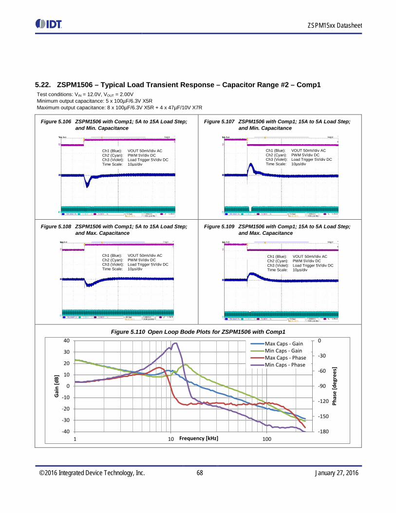
ZSPM15xx Datasheet
© 2016 Integrated Device Technology, Inc. 68 January 27, 2016
5.22. ZSPM1506 – Typical Load Transient Response – Capacitor Range #2 – Comp1 Test conditions: VIN = 12.0V, VOUT = 2.00V Minimum output capacitance: 5 x 100µF/6.3V X5R Maximum output capacitance: 8 x 100µF/6.3V X5R + 4 x 47µF/10V X7R
Figure 5.106 ZSPM1506 with Comp1; 5A to 15A Load Step; and Min. Capacitance
Figure 5.107 ZSPM1506 with Comp1; 15A to 5A Load Step; and Min. Capacitance
Figure 5.108 ZSPM1506 with Comp1; 5A to 15A Load Step; and Max. Capacitance
Figure 5.109 ZSPM1506 with Comp1; 15A to 5A Load Step; and Max. Capacitance
Figure 5.110 Open Loop Bode Plots for ZSPM1506 with Comp1
-180
-150
-120
-90
-60
-30
0
-40
-30
-20
-10
0
10
20
30
40
1 10 100
Phas
e [d
egre
es]
Gai
n [d
B]
Frequency [kHz]
Max Caps - GainMin Caps - GainMax Caps - PhaseMin Caps - Phase
Ch1 (Blue): VOUT 50mV/div AC Ch2 (Cyan): PWM 5V/div DC Ch3 (Violet): Load Trigger 5V/div DC Time Scale: 10µs/div
Ch1 (Blue): VOUT 50mV/div AC Ch2 (Cyan): PWM 5V/div DC Ch3 (Violet): Load Trigger 5V/div DC Time Scale: 10µs/div
Ch1 (Blue): VOUT 50mV/div AC Ch2 (Cyan): PWM 5V/div DC Ch3 (Violet): Load Trigger 5V/div DC Time Scale: 10µs/div
Ch1 (Blue): VOUT 50mV/div AC Ch2 (Cyan): PWM 5V/div DC Ch3 (Violet): Load Trigger 5V/div DC Time Scale: 10µs/div

ZSPM15xx Datasheet
© 2016 Integrated Device Technology, Inc. 69 January 27, 2016
5.23. ZSPM1506 – Typical Load Transient Response – Capacitor Range #3 – Comp2 Test conditions: VIN = 12.0V, VOUT = 2.00V Minimum output capacitance: 2 x 100µF/6.3V X5R + 2 x 470µF/7mΩ Maximum output capacitance: 4 x 100µF/6.3V X5R + 2 x 47µF/10V X7R + 4 x 470µF/7mΩ
Figure 5.111 ZSPM1506 with Comp2; 5A to 15A Load Step; and Min. Capacitance
Figure 5.112 ZSPM1506 with Comp2; 15A to 5A Load Step; and Min. Capacitance
Figure 5.113 ZSPM1506 with Comp2; 5A to 15A Load Step; and Max. Capacitance
Figure 5.114 ZSPM1506 with Comp2; 15A to 5A Load Step; and Max. Capacitance
Figure 5.115 Open Loop Bode Plots for ZSPM1506 with Comp2
-180
-150
-120
-90
-60
-30
0
-40
-30
-20
-10
0
10
20
30
40
1 10 100
Phas
e [d
egre
es]
Gai
n [d
B]
Frequency [kHz]
Max Caps - GainMin Caps - GainMax Caps - PhaseMin Caps - Phase
Ch1 (Blue): VOUT 50mV/div AC Ch2 (Cyan): PWM 5V/div DC Ch3 (Violet): Load Trigger 5V/div DC Time Scale: 10µs/div
Ch1 (Blue): VOUT 50mV/div AC Ch2 (Cyan): PWM 5V/div DC Ch3 (Violet): Load Trigger 5V/div DC Time Scale: 10µs/div
Ch1 (Blue): VOUT 50mV/div AC Ch2 (Cyan): PWM 5V/div DC Ch3 (Violet): Load Trigger 5V/div DC Time Scale: 10µs/div
Ch1 (Blue): VOUT 50mV/div AC Ch2 (Cyan): PWM 5V/div DC Ch3 (Violet): Load Trigger 5V/div DC Time Scale: 10µs/div
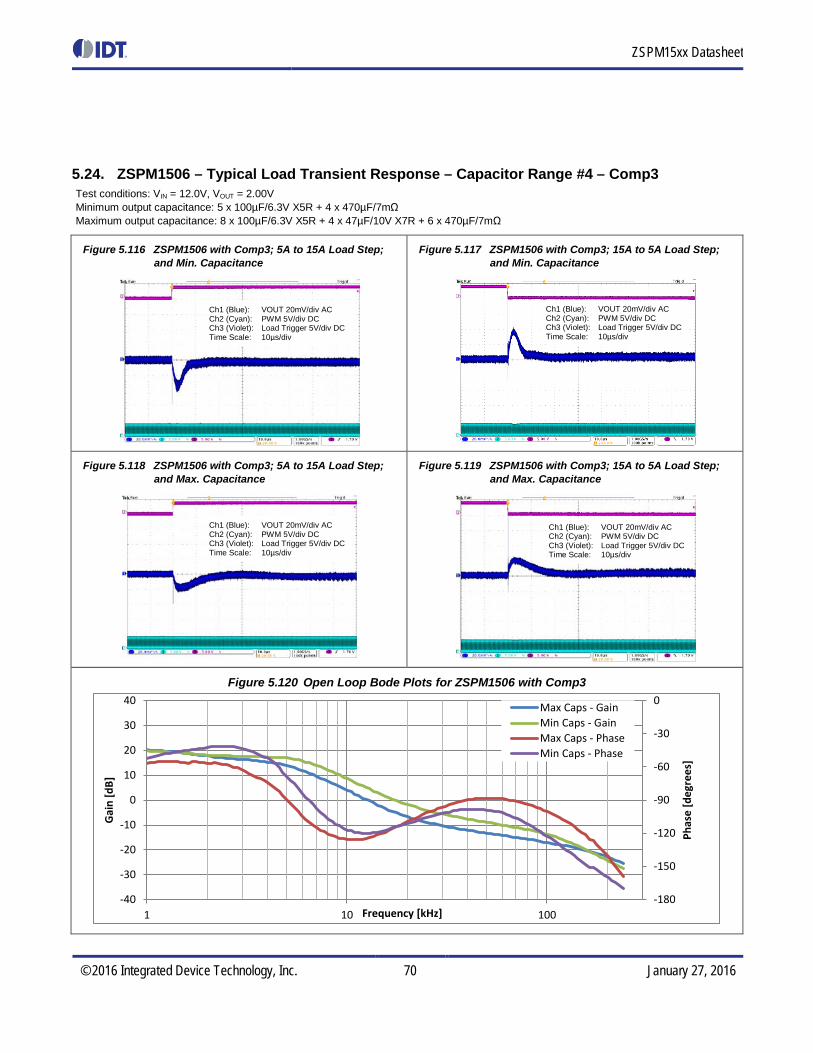
ZSPM15xx Datasheet
© 2016 Integrated Device Technology, Inc. 70 January 27, 2016
5.24. ZSPM1506 – Typical Load Transient Response – Capacitor Range #4 – Comp3 Test conditions: VIN = 12.0V, VOUT = 2.00V Minimum output capacitance: 5 x 100µF/6.3V X5R + 4 x 470µF/7mΩ Maximum output capacitance: 8 x 100µF/6.3V X5R + 4 x 47µF/10V X7R + 6 x 470µF/7mΩ
Figure 5.116 ZSPM1506 with Comp3; 5A to 15A Load Step; and Min. Capacitance
Figure 5.117 ZSPM1506 with Comp3; 15A to 5A Load Step; and Min. Capacitance
Figure 5.118 ZSPM1506 with Comp3; 5A to 15A Load Step; and Max. Capacitance
Figure 5.119 ZSPM1506 with Comp3; 15A to 5A Load Step; and Max. Capacitance
Figure 5.120 Open Loop Bode Plots for ZSPM1506 with Comp3
-180
-150
-120
-90
-60
-30
0
-40
-30
-20
-10
0
10
20
30
40
1 10 100
Phas
e [d
egre
es]
Gai
n [d
B]
Frequency [kHz]
Max Caps - GainMin Caps - GainMax Caps - PhaseMin Caps - Phase
Ch1 (Blue): VOUT 20mV/div AC Ch2 (Cyan): PWM 5V/div DC Ch3 (Violet): Load Trigger 5V/div DC Time Scale: 10µs/div
Ch1 (Blue): VOUT 20mV/div AC Ch2 (Cyan): PWM 5V/div DC Ch3 (Violet): Load Trigger 5V/div DC Time Scale: 10µs/div
Ch1 (Blue): VOUT 20mV/div AC Ch2 (Cyan): PWM 5V/div DC Ch3 (Violet): Load Trigger 5V/div DC Time Scale: 10µs/div
Ch1 (Blue): VOUT 20mV/div AC Ch2 (Cyan): PWM 5V/div DC Ch3 (Violet): Load Trigger 5V/div DC Time Scale: 10µs/div

ZSPM15xx Datasheet
© 2016 Integrated Device Technology, Inc. 71 January 27, 2016
5.25. ZSPM1507 – Typical Load Transient Response –Capacitor Range 1 – Comp0 Test conditions: VIN = 12.0V, VOUT = 2.50V Minimum output capacitance: 2 x 100µF/6.3V X5R Maximum output capacitance: 4 x 100µF/6.3V X5R + 2 x 47µF/10V X7R
Figure 5.121 ZSPM1507 with Comp0; 5 to 15A Load Step; and Min. Capacitance
Figure 5.122 ZSPM1507 with Comp0; 15 to 5A Load Step; and Min. Capacitance
Figure 5.123 ZSPM1507 with Comp0; 5 to 15A Load Step; and Max. Capacitance
Figure 5.124 ZSPM1507 with Comp0; 15 to 5A Load Step; and Max. Capacitance
Figure 5.125 Open Loop Bode Plots for ZSPM1507 with Comp0
-180
-150
-120
-90
-60
-30
0
-40
-30
-20
-10
0
10
20
30
40
1 10 100
Phas
e [d
egre
es]
Gai
n [d
B]
Frequency [kHz]
Max Caps - GainMin Caps - GainMax Caps - PhaseMin Caps - Phase
Ch1 (Blue): VOUT 100mV/div AC Ch2 (Cyan): PWM 5V/div DC Ch3 (Violet): Load Trigger 5V/div DC Time Scale: 10µs/div
Ch1 (Blue): VOUT 100mV/div AC Ch2 (Cyan): PWM 5V/div DC Ch3 (Violet): Load Trigger 5V/div DC Time Scale: 10µs/div
Ch1 (Blue): VOUT 100mV/div AC Ch2 (Cyan): PWM 5V/div DC Ch3 (Violet): Load Trigger 5V/div DC Time Scale: 10µs/div
Ch1 (Blue): VOUT 100mV/div AC Ch2 (Cyan): PWM 5V/div DC Ch3 (Violet): Load Trigger 5V/div DC Time Scale: 10µs/div
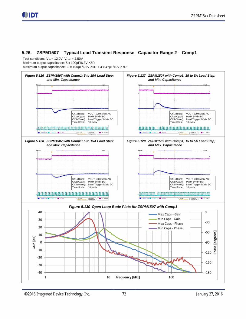
ZSPM15xx Datasheet
© 2016 Integrated Device Technology, Inc. 72 January 27, 2016
5.26. ZSPM1507 – Typical Load Transient Response –Capacitor Range 2 – Comp1 Test conditions: VIN = 12.0V, VOUT = 2.50V Minimum output capacitance: 5 x 100µF/6.3V X5R Maximum output capacitance: 8 x 100µF/6.3V X5R + 4 x 47µF/10V X7R
Figure 5.126 ZSPM1507 with Comp1; 5 to 15A Load Step; and Min. Capacitance
Figure 5.127 ZSPM1507 with Comp1; 15 to 5A Load Step; and Min. Capacitance
Figure 5.128 ZSPM1507 with Comp1; 5 to 15A Load Step; and Max. Capacitance
Figure 5.129 ZSPM1507 with Comp1; 15 to 5A Load Step; and Max. Capacitance
Figure 5.130 Open Loop Bode Plots for ZSPM1507 with Comp1
-180
-150
-120
-90
-60
-30
0
-40
-30
-20
-10
0
10
20
30
40
1 10 100
Phas
e [d
egre
es]
Gai
n [d
B]
Frequency [kHz]
Max Caps - GainMin Caps - GainMax Caps - PhaseMin Caps - Phase
Ch1 (Blue): VOUT 100mV/div AC Ch2 (Cyan): PWM 5V/div DC Ch3 (Violet): Load Trigger 5V/div DC Time Scale: 10µs/div
Ch1 (Blue): VOUT 100mV/div AC Ch2 (Cyan): PWM 5V/div DC Ch3 (Violet): Load Trigger 5V/div DC Time Scale: 10µs/div
Ch1 (Blue): VOUT 100mV/div AC Ch2 (Cyan): PWM 5V/div DC Ch3 (Violet): Load Trigger 5V/div DC Time Scale: 10µs/div
Ch1 (Blue): VOUT 100mV/div AC Ch2 (Cyan): PWM 5V/div DC Ch3 (Violet): Load Trigger 5V/div DC Time Scale: 10µs/div

ZSPM15xx Datasheet
© 2016 Integrated Device Technology, Inc. 73 January 27, 2016
5.27. ZSPM1507 – Typical Load Transient Response –Capacitor Range 3 – Comp2 Test conditions: VIN = 12.0V, VOUT = 2.50V Minimum output capacitance: 2 x 100µF/6.3V X5R + 2x 470µF/7mΩ Maximum output capacitance: 4 x 100µF/6.3V X5R + 2 x 47µF/10V X7R + 4 x 470µF/7mΩ
Figure 5.131 ZSPM1507 with Comp2; 5 to 15A Load Step; and Min. Capacitance
Figure 5.132 ZSPM1507 with Comp2; 15 to 5A Load Step; and Min. Capacitance
Figure 5.133 ZSPM1507 with Comp2; 5 to 15A Load Step; and Max. Capacitance
Figure 5.134 ZSPM1507 with Comp2; 15 to 5A Load Step; and Max. Capacitance
Figure 5.135 Open Loop Bode Plots for ZSPM1507 with Comp2
-180
-150
-120
-90
-60
-30
0
-40
-30
-20
-10
0
10
20
30
40
1 10 100
Phas
e [d
egre
es]
Gai
n [d
B]
Frequency [kHz]
Max Caps - GainMin Caps - GainMax Caps - PhaseMin Caps - Phase
Ch1 (Blue): VOUT 100mV/div AC Ch2 (Cyan): PWM 5V/div DC Ch3 (Violet): Load Trigger 5V/div DC Time Scale: 10µs/div
Ch1 (Blue): VOUT 100mV/div AC Ch2 (Cyan): PWM 5V/div DC Ch3 (Violet): Load Trigger 5V/div DC Time Scale: 10µs/div
Ch1 (Blue): VOUT 100mV/div AC Ch2 (Cyan): PWM 5V/div DC Ch3 (Violet): Load Trigger 5V/div DC Time Scale: 10µs/div
Ch1 (Blue): VOUT 100mV/div AC Ch2 (Cyan): PWM 5V/div DC Ch3 (Violet): Load Trigger 5V/div DC Time Scale: 10µs/div

ZSPM15xx Datasheet
© 2016 Integrated Device Technology, Inc. 74 January 27, 2016
5.28. ZSPM1507 – Typical Load Transient Response –Capacitor Range 4 – Comp3 Test conditions: VIN = 12.0V, VOUT = 2.50V Minimum output capacitance: 5 x 100µF/6.3V X5R + 4 x 470µF/7mΩ Maximum output capacitance: 8 x 100µF/6.3V X5R + 4 x 47µF/10V X7R + 6 x 470µF/7mΩ
Figure 5.136 ZSPM1507 with Comp3; 5 to 15A Load Step; and Min. Capacitance
Figure 5.137 ZSPM1507 with Comp3; 15 to 5A Load Step; and Min. Capacitance
Figure 5.138 ZSPM1507 with Comp3; 5 to 15A Load Step; and Max. Capacitance
Figure 5.139 ZSPM1507 with Comp3; 15 to 5A Load Step; and Max. Capacitance
Figure 5.140 Open Loop Bode Plots for ZSPM1507 with Comp3
-180
-150
-120
-90
-60
-30
0
-40
-30
-20
-10
0
10
20
30
40
1 10 100
Phas
e [d
egre
es]
Gai
n [d
B]
Frequency [kHz]
Max Caps - GainMin Caps - GainMax Caps - PhaseMin Caps - Phase
Ch1 (Blue): VOUT 100mV/div AC Ch2 (Cyan): PWM 5V/div DC Ch3 (Violet): Load Trigger 5V/div DC Time Scale: 10µs/div
Ch1 (Blue): VOUT 100mV/div AC Ch2 (Cyan): PWM 5V/div DC Ch3 (Violet): Load Trigger 5V/div DC Time Scale: 10µs/div
Ch1 (Blue): VOUT 100mV/div AC Ch2 (Cyan): PWM 5V/div DC Ch3 (Violet): Load Trigger 5V/div DC Time Scale: 10µs/div
Ch1 (Blue): VOUT 100mV/div AC Ch2 (Cyan): PWM 5V/div DC Ch3 (Violet): Load Trigger 5V/div DC Time Scale: 10µs/div

ZSPM15xx Datasheet
© 2016 Integrated Device Technology, Inc. 75 January 27, 2016
5.29. ZSPM1508 – Typical Load Transient Response –Capacitor Range 1 – Comp0 Test conditions: VIN = 12.0V, VOUT = 3.30V Minimum output capacitance: 2 x 100µF/10V X5R Maximum output capacitance: 4 x 100µF/10V X5R + 2 x 47µF/10V X7R
Figure 5.141 ZSPM1508 with Comp0; 5A to 10A Load Step; and Min. Capacitance
Figure 5.142 ZSPM1508 with Comp0; 10A to 5A Load Step; and Min. Capacitance
Figure 5.143 ZSPM1508 with Comp0; 5A to 10A Load Step; and Max. Capacitance
Figure 5.144 ZSPM1508 with Comp0; 10A to 5A Load Step; and Max. Capacitance
Figure 5.145 Open Loop Bode Plots for ZSPM1508 with Comp0
-180-150-120-90-60-300306090120150180
-40
-30
-20
-10
0
10
20
30
40
0.1 1 10 100
Phas
e [d
egre
es]
Gai
n [d
B]
Frequency [kHz]
Max Caps - GainMin Caps - GainMax Caps - PhaseMin Caps - Phase
Ch1 (Blue): VOUT 50mV/div AC Ch2 (Cyan): PWM 5V/div DC Ch3 (Violet): Load Trigger 5V/div DC Time Scale: 10µs/div
Ch1 (Blue): VOUT 50mV/div AC Ch2 (Cyan): PWM 5V/div DC Ch3 (Violet): Load Trigger 5V/div DC Time Scale: 10µs/div
Ch1 (Blue): VOUT 50mV/div AC Ch2 (Cyan): PWM 5V/div DC Ch3 (Violet): Load Trigger 5V/div DC Time Scale: 10µs/div
Ch1 (Blue): VOUT 50mV/div AC Ch2 (Cyan): PWM 5V/div DC Ch3 (Violet): Load Trigger 5V/div DC Time Scale: 10µs/div

ZSPM15xx Datasheet
© 2016 Integrated Device Technology, Inc. 76 January 27, 2016
5.30. ZSPM1508 – Typical Load Transient Response –Capacitor Range 2 – Comp1 Test conditions: VIN = 12.0V, VOUT = 3.30V Minimum output capacitance: 5 x 100µF/10V X5R Maximum output capacitance: 8 x 100µF/10V X5R + 4 x 47µF/10V X7R
Figure 5.146 ZSPM1508 with Comp1; 5A to 10A Load Step; and Min. Capacitance
Figure 5.147 ZSPM1508 with Comp1; 10A to 5A Load Step; and Min. Capacitance
Figure 5.148 ZSPM1508 with Comp1; 5A to 10A Load Step; and Max. Capacitance
Figure 5.149 ZSPM1508 with Comp1; 10A to 5A Load Step; and Max. Capacitance
Figure 5.150 Open Loop Bode Plots for ZSPM1508 with Comp1
-180-150-120-90-60-300306090120150180
-40
-30
-20
-10
0
10
20
30
40
0.1 1 10 100
Phas
e [d
egre
es]
Gai
n [d
B]
Frequency [kHz]
Max Caps - GainMin Caps - GainMax Caps - PhaseMin Caps - Phase
Ch1 (Blue): VOUT 50mV/div AC Ch2 (Cyan): PWM 5V/div DC Ch3 (Violet): Load Trigger 5V/div DC Time Scale: 10µs/div
Ch1 (Blue): VOUT 50mV/div AC Ch2 (Cyan): PWM 5V/div DC Ch3 (Violet): Load Trigger 5V/div DC Time Scale: 10µs/div
Ch1 (Blue): VOUT 50mV/div AC Ch2 (Cyan): PWM 5V/div DC Ch3 (Violet): Load Trigger 5V/div DC Time Scale: 10µs/div
Ch1 (Blue): VOUT 50mV/div AC Ch2 (Cyan): PWM 5V/div DC Ch3 (Violet): Load Trigger 5V/div DC Time Scale: 10µs/div
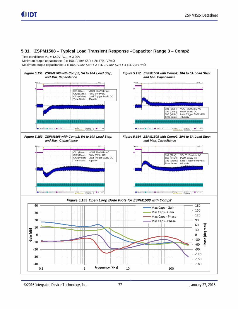
ZSPM15xx Datasheet
© 2016 Integrated Device Technology, Inc. 77 January 27, 2016
5.31. ZSPM1508 – Typical Load Transient Response –Capacitor Range 3 – Comp2 Test conditions: VIN = 12.0V, VOUT = 3.30V Minimum output capacitance: 2 x 100µF/10V X5R + 2x 470µF/7mΩ Maximum output capacitance: 4 x 100µF/10V X5R + 2 x 47µF/10V X7R + 4 x 470µF/7mΩ
Figure 5.151 ZSPM1508 with Comp2; 5A to 10A Load Step; and Min. Capacitance
Figure 5.152 ZSPM1508 with Comp2; 10A to 5A Load Step; and Min. Capacitance
Figure 5.153 ZSPM1508 with Comp2; 5A to 10A Load Step; and Max. Capacitance
Figure 5.154 ZSPM1508 with Comp2; 10A to 5A Load Step; and Max. Capacitance
Figure 5.155 Open Loop Bode Plots for ZSPM1508 with Comp2
-180-150-120-90-60-300306090120150180
-40
-30
-20
-10
0
10
20
30
40
0.1 1 10 100
Phas
e [d
egre
es]
Gai
n [d
B]
Frequency [kHz]
Max Caps - GainMin Caps - GainMax Caps - PhaseMin Caps - Phase
Ch1 (Blue): VOUT 20mV/div AC Ch2 (Cyan): PWM 5V/div DC Ch3 (Violet): Load Trigger 5V/div DC Time Scale: 40µs/div
Ch1 (Blue): VOUT 20mV/div AC Ch2 (Cyan): PWM 5V/div DC Ch3 (Violet): Load Trigger 5V/div DC Time Scale: 40µs/div
Ch1 (Blue): VOUT 20mV/div AC Ch2 (Cyan): PWM 5V/div DC Ch3 (Violet): Load Trigger 5V/div DC Time Scale: 40µs/div
Ch1 (Blue): VOUT 20mV/div AC Ch2 (Cyan): PWM 5V/div DC Ch3 (Violet): Load Trigger 5V/div DC Time Scale: 40µs/div
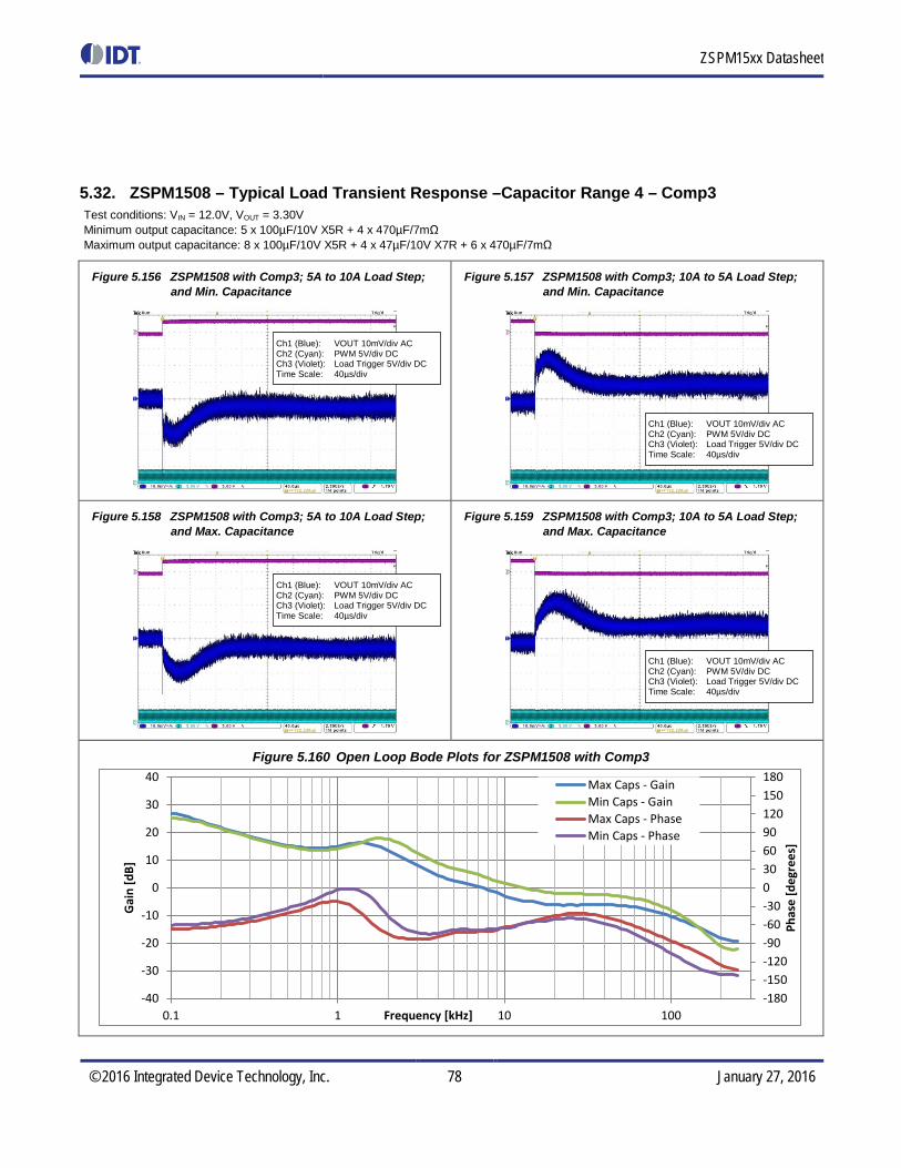
ZSPM15xx Datasheet
© 2016 Integrated Device Technology, Inc. 78 January 27, 2016
5.32. ZSPM1508 – Typical Load Transient Response –Capacitor Range 4 – Comp3 Test conditions: VIN = 12.0V, VOUT = 3.30V Minimum output capacitance: 5 x 100µF/10V X5R + 4 x 470µF/7mΩ Maximum output capacitance: 8 x 100µF/10V X5R + 4 x 47µF/10V X7R + 6 x 470µF/7mΩ
Figure 5.156 ZSPM1508 with Comp3; 5A to 10A Load Step; and Min. Capacitance
Figure 5.157 ZSPM1508 with Comp3; 10A to 5A Load Step; and Min. Capacitance
Figure 5.158 ZSPM1508 with Comp3; 5A to 10A Load Step; and Max. Capacitance
Figure 5.159 ZSPM1508 with Comp3; 10A to 5A Load Step; and Max. Capacitance
Figure 5.160 Open Loop Bode Plots for ZSPM1508 with Comp3
-180-150-120-90-60-300306090120150180
-40
-30
-20
-10
0
10
20
30
40
0.1 1 10 100
Phas
e [d
egre
es]
Gai
n [d
B]
Frequency [kHz]
Max Caps - GainMin Caps - GainMax Caps - PhaseMin Caps - Phase
Ch1 (Blue): VOUT 10mV/div AC Ch2 (Cyan): PWM 5V/div DC Ch3 (Violet): Load Trigger 5V/div DC Time Scale: 40µs/div
Ch1 (Blue): VOUT 10mV/div AC Ch2 (Cyan): PWM 5V/div DC Ch3 (Violet): Load Trigger 5V/div DC Time Scale: 40µs/div
Ch1 (Blue): VOUT 10mV/div AC Ch2 (Cyan): PWM 5V/div DC Ch3 (Violet): Load Trigger 5V/div DC Time Scale: 40µs/div
Ch1 (Blue): VOUT 10mV/div AC Ch2 (Cyan): PWM 5V/div DC Ch3 (Violet): Load Trigger 5V/div DC Time Scale: 40µs/div
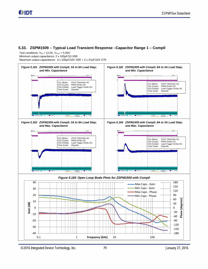
ZSPM15xx Datasheet
© 2016 Integrated Device Technology, Inc. 79 January 27, 2016
5.33. ZSPM1509 – Typical Load Transient Response –Capacitor Range 1 – Comp0 Test conditions: VIN = 12.0V, VOUT = 5.00V Minimum output capacitance: 2 x 100µF/10 X5R Maximum output capacitance: 4 x 100µF/10V X5R + 2 x 47µF/10V X7R
Figure 5.161 ZSPM1509 with Comp0; 3A to 8A Load Step; and Min. Capacitance
Figure 5.162 ZSPM1509 with Comp0; 8A to 3A Load Step; and Min. Capacitance
Figure 5.163 ZSPM1509 with Comp0; 3A to 8A Load Step; and Max. Capacitance
Figure 5.164 ZSPM1509 with Comp0; 8A to 3A Load Step; and Max. Capacitance
Figure 5.165 Open Loop Bode Plots for ZSPM1509 with Comp0
-180-150-120-90-60-300306090120150180
-40
-30
-20
-10
0
10
20
30
40
0.1 1 10 100
Phas
e [d
egre
es]
Gai
n [d
B]
Frequency [kHz]
Max Caps - GainMin Caps - GainMax Caps - PhaseMin Caps - Phase
Ch1 (Blue): VOUT 50mV/div AC Ch2 (Cyan): PWM 5V/div DC Ch3 (Violet): Load Trigger 5V/div DC Time Scale: 20µs/div
Ch1 (Blue): VOUT 50mV/div AC Ch2 (Cyan): PWM 5V/div DC Ch3 (Violet): Load Trigger 5V/div DC Time Scale: 20µs/div
Ch1 (Blue): VOUT 50mV/div AC Ch2 (Cyan): PWM 5V/div DC Ch3 (Violet): Load Trigger 5V/div DC Time Scale: 20µs/div
Ch1 (Blue): VOUT 50mV/div AC Ch2 (Cyan): PWM 5V/div DC Ch3 (Violet): Load Trigger 5V/div DC Time Scale: 20µs/div
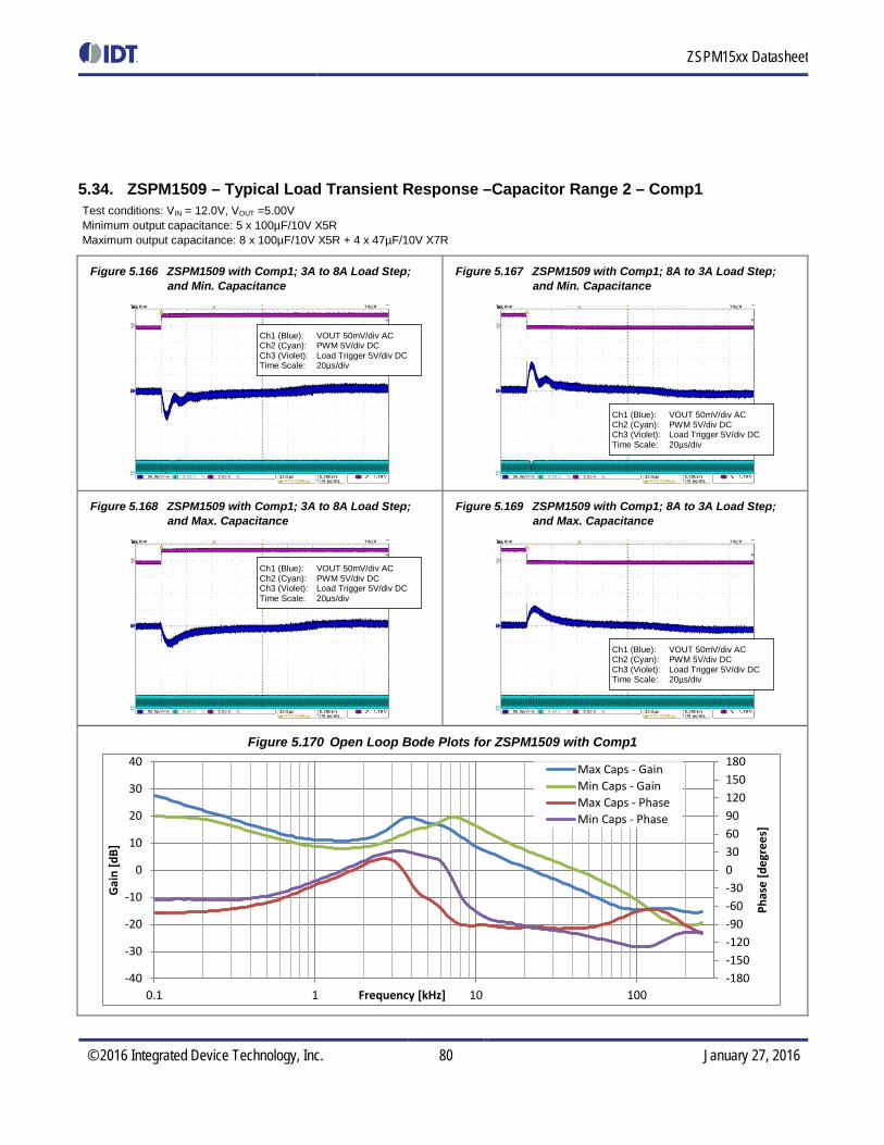
ZSPM15xx Datasheet
© 2016 Integrated Device Technology, Inc. 80 January 27, 2016
5.34. ZSPM1509 – Typical Load Transient Response –Capacitor Range 2 – Comp1 Test conditions: VIN = 12.0V, VOUT =5.00V Minimum output capacitance: 5 x 100µF/10V X5R Maximum output capacitance: 8 x 100µF/10V X5R + 4 x 47µF/10V X7R
Figure 5.166 ZSPM1509 with Comp1; 3A to 8A Load Step; and Min. Capacitance
Figure 5.167 ZSPM1509 with Comp1; 8A to 3A Load Step; and Min. Capacitance
Figure 5.168 ZSPM1509 with Comp1; 3A to 8A Load Step; and Max. Capacitance
Figure 5.169 ZSPM1509 with Comp1; 8A to 3A Load Step; and Max. Capacitance
Figure 5.170 Open Loop Bode Plots for ZSPM1509 with Comp1
-180-150-120-90-60-300306090120150180
-40
-30
-20
-10
0
10
20
30
40
0.1 1 10 100
Phas
e [d
egre
es]
Gai
n [d
B]
Frequency [kHz]
Max Caps - GainMin Caps - GainMax Caps - PhaseMin Caps - Phase
Ch1 (Blue): VOUT 50mV/div AC Ch2 (Cyan): PWM 5V/div DC Ch3 (Violet): Load Trigger 5V/div DC Time Scale: 20µs/div
Ch1 (Blue): VOUT 50mV/div AC Ch2 (Cyan): PWM 5V/div DC Ch3 (Violet): Load Trigger 5V/div DC Time Scale: 20µs/div
Ch1 (Blue): VOUT 50mV/div AC Ch2 (Cyan): PWM 5V/div DC Ch3 (Violet): Load Trigger 5V/div DC Time Scale: 20µs/div
Ch1 (Blue): VOUT 50mV/div AC Ch2 (Cyan): PWM 5V/div DC Ch3 (Violet): Load Trigger 5V/div DC Time Scale: 20µs/div
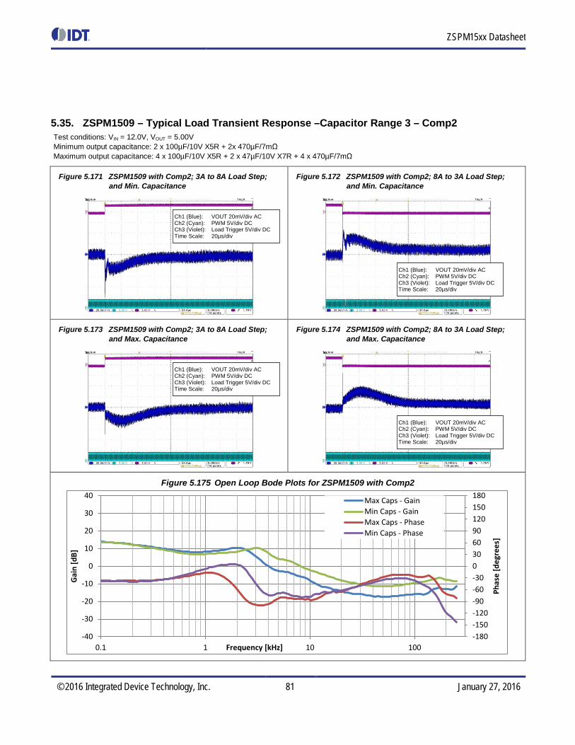
ZSPM15xx Datasheet
© 2016 Integrated Device Technology, Inc. 81 January 27, 2016
5.35. ZSPM1509 – Typical Load Transient Response –Capacitor Range 3 – Comp2 Test conditions: VIN = 12.0V, VOUT = 5.00V Minimum output capacitance: 2 x 100µF/10V X5R + 2x 470µF/7mΩ Maximum output capacitance: 4 x 100µF/10V X5R + 2 x 47µF/10V X7R + 4 x 470µF/7mΩ
Figure 5.171 ZSPM1509 with Comp2; 3A to 8A Load Step; and Min. Capacitance
Figure 5.172 ZSPM1509 with Comp2; 8A to 3A Load Step; and Min. Capacitance
Figure 5.173 ZSPM1509 with Comp2; 3A to 8A Load Step; and Max. Capacitance
Figure 5.174 ZSPM1509 with Comp2; 8A to 3A Load Step; and Max. Capacitance
Figure 5.175 Open Loop Bode Plots for ZSPM1509 with Comp2
-180-150-120-90-60-300306090120150180
-40
-30
-20
-10
0
10
20
30
40
0.1 1 10 100
Phas
e [d
egre
es]
Gai
n [d
B]
Frequency [kHz]
Max Caps - GainMin Caps - GainMax Caps - PhaseMin Caps - Phase
Ch1 (Blue): VOUT 20mV/div AC Ch2 (Cyan): PWM 5V/div DC Ch3 (Violet): Load Trigger 5V/div DC Time Scale: 20µs/div
Ch1 (Blue): VOUT 20mV/div AC Ch2 (Cyan): PWM 5V/div DC Ch3 (Violet): Load Trigger 5V/div DC Time Scale: 20µs/div
Ch1 (Blue): VOUT 20mV/div AC Ch2 (Cyan): PWM 5V/div DC Ch3 (Violet): Load Trigger 5V/div DC Time Scale: 20µs/div
Ch1 (Blue): VOUT 20mV/div AC Ch2 (Cyan): PWM 5V/div DC Ch3 (Violet): Load Trigger 5V/div DC Time Scale: 20µs/div

ZSPM15xx Datasheet
© 2016 Integrated Device Technology, Inc. 82 January 27, 2016
5.36. ZSPM1509 – Typical Load Transient Response –Capacitor Range 4 – Comp3 Test conditions: VIN = 12.0V, VOUT =5.00V Minimum output capacitance: 5 x 100µF/10V X5R + 4 x 470µF/7mΩ Maximum output capacitance: 8 x 100µF/10V X5R + 4 x 47µF/10V X7R + 6 x 470µF/7mΩ
Figure 5.176 ZSPM1509 with Comp3; 3A to 8A Load Step; and Min. Capacitance
Figure 5.177 ZSPM1509 with Comp3; 8A to 3A Load Step; and Min. Capacitance
Figure 5.178 ZSPM1509 with Comp3; 3A to 8A Load Step; and Max. Capacitance
Figure 5.179 ZSPM1509 with Comp3; 8A to 3A Load Step; and Max. Capacitance
Figure 5.180 Open Loop Bode Plots for ZSPM1509 with Comp3
-180-150-120-90-60-300306090120150180
-40
-30
-20
-10
0
10
20
30
40
0.1 1 10 100
Phas
e [d
egre
es]
Gai
n [d
B]
Frequency [kHz]
Max Caps - GainMin Caps - GainMax Caps - PhaseMin Caps - Phase
Ch1 (Blue): VOUT 20mV/div AC Ch2 (Cyan): PWM 5V/div DC Ch3:(Violet): Load Trigger 5V/div DC Time Scale: 100µs/div
Ch1 (Blue): VOUT 20mV/div AC Ch2 (Cyan): PWM 5V/div DC Ch3 (Violet): Load Trigger 5V/div DC Time Scale: 100µs/div
Ch1 (Blue): VOUT 20mV/div AC Ch2 (Cyan): PWM 5V/div DC Ch3 (Violet): Load Trigger 5V/div DC Time Scale: 100µs/div
Ch1 (Blue): VOUT 20mV/div AC Ch2 (Cyan): PWM 5V/div DC Ch3 (Violet): Load Trigger 5V/div DC Time Scale: 100µs/div

ZSPM15xx Datasheet
© 2016 Integrated Device Technology, Inc. 83 January 27, 2016
5.37. ZSPM1511 – Typical Load Transient Response – Capacitor Range #1 – Comp0 Test conditions: VIN = 12.0V, VOUT = 0.85V Minimum output capacitance: 2 x 100µF/6.3V X5R Maximum output capacitance: 4 x 100µF/6.3V X5R + 2 x 47µF/10V X7R
Figure 5.181 ZSPM1511 with Comp0; 5A to 15A Load Step; and Min. Capacitance
Figure 5.182 ZSPM1511 with Comp0; 15A to 5A Load Step; and Min. Capacitance
Figure 5.183 ZSPM1511 with Comp0; 5A to 15A Load Step; and Max. Capacitance
Figure 5.184 ZSPM1511 with Comp0; 15A to 5A Load Step; and Max. Capacitance
Figure 5.185 Open Loop Bode Plots for ZSPM1511 with Comp0
-180-150-120-90-60-300306090120150180
-40
-30
-20
-10
0
10
20
30
40
1 10 100
Phas
e [d
egre
es]
Gai
n [d
B]
Frequency [kHz]
Max Caps - GainMin Caps - GainMax Caps - PhaseMin Caps - Phase
Ch1 (Blue): VOUT 50mV/div AC Ch2 (Cyan): PWM 5V/div DC Ch4 (Violet): Load Trigger 5V/div DC Time Scale: 10µs/div
Ch1 (Blue): VOUT 50mV/div AC Ch2 (Cyan): PWM 5V/div DC Ch4 (Violet): Load Trigger 5V/div DC Time Scale: 10µs/div
Ch1 (Blue): VOUT 50mV/div AC Ch2 (Cyan): PWM 5V/div DC Ch4 (Violet): Load Trigger 5V/div DC Time Scale: 10µs/div
Ch1 (Blue): VOUT 50mV/div AC Ch2 (Cyan): PWM 5V/div DC Ch4 (Violet): Load Trigger 5V/div DC Time Scale: 10µs/div

ZSPM15xx Datasheet
© 2016 Integrated Device Technology, Inc. 84 January 27, 2016
5.38. ZSPM1511 – Typical Load Transient Response – Capacitor Range #2 – Comp1 Test conditions: VIN = 12.0V, VOUT = 0.85V Minimum output capacitance: 5 x 100µF/6.3V X5R Maximum output capacitance: 8 x 100µF/6.3V X5R + 4 x 47µF/10V X7R
Figure 5.186 ZSPM1511 with Comp1; 5A to 15A Load Step; and Min. Capacitance
Figure 5.187 ZSPM1511 with Comp1; 15A to 5A Load Step; and Min. Capacitance
Figure 5.188 ZSPM1511 with Comp1; 5A to 15A Load Step; and Max. Capacitance
Figure 5.189 ZSPM1511 with Comp1; 15A to 5A Load Step; and Max. Capacitance
Figure 5.190 Open Loop Bode Plots for ZSPM1511 with Comp1
-180-150-120-90-60-300306090120150180
-40
-30
-20
-10
0
10
20
30
40
1 10 100
Phas
e [d
egre
es]
Gai
n [d
B]
Frequency [kHz]
Max Caps - GainMin Caps - GainMax Caps - PhaseMin Caps - Phase
Ch1 (Blue): VOUT 50mV/div AC Ch2 (Cyan): PWM 5V/div DC Ch3 (Violet): Load Trigger 5V/div DC Time Scale: 10µs/div
Ch1 (Blue): VOUT 20mV/div AC Ch2 (Cyan): PWM 5V/div DC Ch3 (Violet): Load Trigger 5V/div DC Time Scale: 10µs/div
Ch1 (Blue): VOUT 50mV/div AC Ch2 (Cyan): PWM 5V/div DC Ch3 (Violet): Load Trigger 5V/div DC Time Scale: 10µs/div
Ch1 (Blue): VOUT 20mV/div AC Ch2 (Cyan): PWM 5V/div DC Ch3 (Violet): Load Trigger 5V/div DC Time Scale: 10µs/div
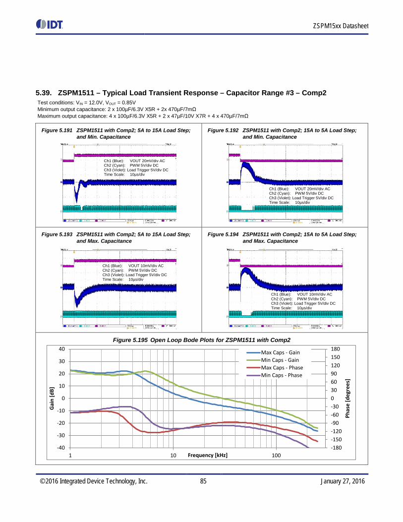
ZSPM15xx Datasheet
© 2016 Integrated Device Technology, Inc. 85 January 27, 2016
5.39. ZSPM1511 – Typical Load Transient Response – Capacitor Range #3 – Comp2 Test conditions: VIN = 12.0V, VOUT = 0.85V Minimum output capacitance: 2 x 100µF/6.3V X5R + 2x 470µF/7mΩ Maximum output capacitance: 4 x 100µF/6.3V X5R + 2 x 47µF/10V X7R + 4 x 470µF/7mΩ
Figure 5.191 ZSPM1511 with Comp2; 5A to 15A Load Step; and Min. Capacitance
Figure 5.192 ZSPM1511 with Comp2; 15A to 5A Load Step; and Min. Capacitance
Figure 5.193 ZSPM1511 with Comp2; 5A to 15A Load Step; and Max. Capacitance
Figure 5.194 ZSPM1511 with Comp2; 15A to 5A Load Step; and Max. Capacitance
Figure 5.195 Open Loop Bode Plots for ZSPM1511 with Comp2
-180-150-120-90-60-300306090120150180
-40
-30
-20
-10
0
10
20
30
40
1 10 100
Phas
e [d
egre
es]
Gai
n [d
B]
Frequency [kHz]
Max Caps - GainMin Caps - GainMax Caps - PhaseMin Caps - Phase
Ch1 (Blue): VOUT 20mV/div AC Ch2 (Cyan): PWM 5V/div DC Ch3 (Violet): Load Trigger 5V/div DC Time Scale: 10µs/div
Ch1 (Blue): VOUT 20mV/div AC Ch2 (Cyan): PWM 5V/div DC Ch3 (Violet): Load Trigger 5V/div DC Time Scale: 10µs/div
Ch1 (Blue): VOUT 10mV/div AC Ch2 (Cyan): PWM 5V/div DC Ch3 (Violet): Load Trigger 5V/div DC Time Scale: 10µs/div
Ch1 (Blue): VOUT 10mV/div AC Ch2 (Cyan): PWM 5V/div DC Ch3 (Violet): Load Trigger 5V/div DC Time Scale: 10µs/div
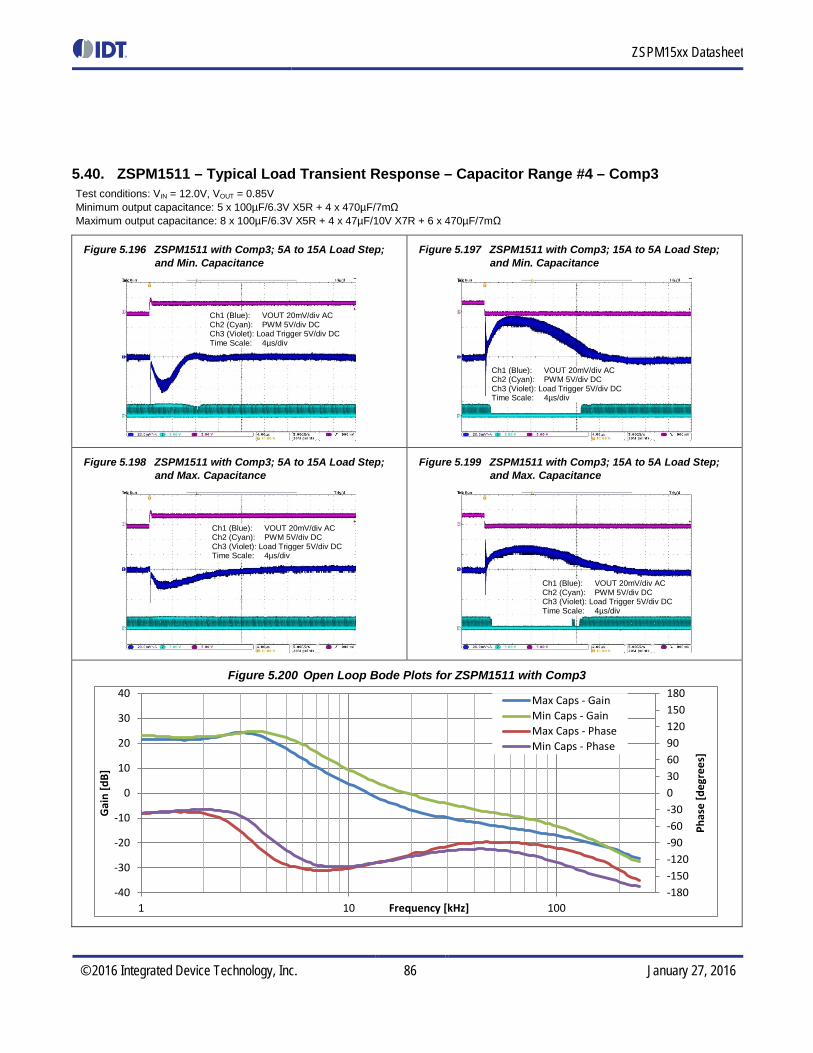
ZSPM15xx Datasheet
© 2016 Integrated Device Technology, Inc. 86 January 27, 2016
5.40. ZSPM1511 – Typical Load Transient Response – Capacitor Range #4 – Comp3 Test conditions: VIN = 12.0V, VOUT = 0.85V Minimum output capacitance: 5 x 100µF/6.3V X5R + 4 x 470µF/7mΩ Maximum output capacitance: 8 x 100µF/6.3V X5R + 4 x 47µF/10V X7R + 6 x 470µF/7mΩ
Figure 5.196 ZSPM1511 with Comp3; 5A to 15A Load Step; and Min. Capacitance
Figure 5.197 ZSPM1511 with Comp3; 15A to 5A Load Step; and Min. Capacitance
Figure 5.198 ZSPM1511 with Comp3; 5A to 15A Load Step; and Max. Capacitance
Figure 5.199 ZSPM1511 with Comp3; 15A to 5A Load Step; and Max. Capacitance
Figure 5.200 Open Loop Bode Plots for ZSPM1511 with Comp3
-180-150-120-90-60-300306090120150180
-40
-30
-20
-10
0
10
20
30
40
1 10 100
Phas
e [d
egre
es]
Gai
n [d
B]
Frequency [kHz]
Max Caps - GainMin Caps - GainMax Caps - PhaseMin Caps - Phase
Ch1 (Blue): VOUT 20mV/div AC Ch2 (Cyan): PWM 5V/div DC Ch3 (Violet): Load Trigger 5V/div DC Time Scale: 4µs/div
Ch1 (Blue): VOUT 20mV/div AC Ch2 (Cyan): PWM 5V/div DC Ch3 (Violet): Load Trigger 5V/div DC Time Scale: 4µs/div
Ch1 (Blue): VOUT 20mV/div AC Ch2 (Cyan): PWM 5V/div DC Ch3 (Violet): Load Trigger 5V/div DC Time Scale: 4µs/div
Ch1 (Blue): VOUT 20mV/div AC Ch2 (Cyan): PWM 5V/div DC Ch3 (Violet): Load Trigger 5V/div DC Time Scale: 4µs/div
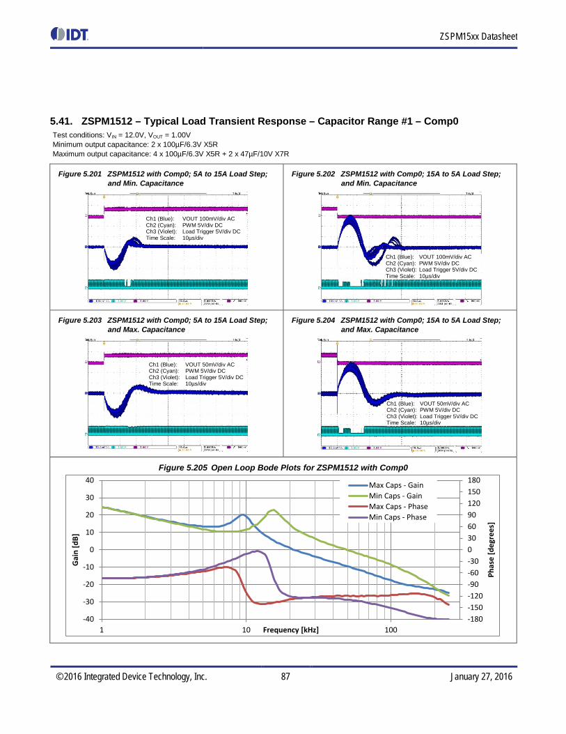
ZSPM15xx Datasheet
© 2016 Integrated Device Technology, Inc. 87 January 27, 2016
5.41. ZSPM1512 – Typical Load Transient Response – Capacitor Range #1 – Comp0 Test conditions: VIN = 12.0V, VOUT = 1.00V Minimum output capacitance: 2 x 100µF/6.3V X5R Maximum output capacitance: 4 x 100µF/6.3V X5R + 2 x 47µF/10V X7R
Figure 5.201 ZSPM1512 with Comp0; 5A to 15A Load Step; and Min. Capacitance
Figure 5.202 ZSPM1512 with Comp0; 15A to 5A Load Step; and Min. Capacitance
Figure 5.203 ZSPM1512 with Comp0; 5A to 15A Load Step; and Max. Capacitance
Figure 5.204 ZSPM1512 with Comp0; 15A to 5A Load Step; and Max. Capacitance
Figure 5.205 Open Loop Bode Plots for ZSPM1512 with Comp0
-180-150-120-90-60-300306090120150180
-40
-30
-20
-10
0
10
20
30
40
1 10 100
Phas
e [d
egre
es]
Gai
n [d
B]
Frequency [kHz]
Max Caps - GainMin Caps - GainMax Caps - PhaseMin Caps - Phase
Ch1 (Blue): VOUT 100mV/div AC Ch2 (Cyan): PWM 5V/div DC Ch3 (Violet): Load Trigger 5V/div DC Time Scale: 10µs/div
Ch1 (Blue): VOUT 50mV/div AC Ch2 (Cyan): PWM 5V/div DC Ch3 (Violet): Load Trigger 5V/div DC Time Scale: 10µs/div
Ch1 (Blue): VOUT 100mV/div AC Ch2 (Cyan): PWM 5V/div DC Ch3 (Violet): Load Trigger 5V/div DC Time Scale: 10µs/div
Ch1 (Blue): VOUT 50mV/div AC Ch2 (Cyan): PWM 5V/div DC Ch3 (Violet): Load Trigger 5V/div DC Time Scale: 10µs/div

ZSPM15xx Datasheet
© 2016 Integrated Device Technology, Inc. 88 January 27, 2016
5.42. ZSPM1512 – Typical Load Transient Response – Capacitor Range #2 – Comp1 Test conditions: VIN = 12.0V, VOUT = 1.00V Minimum output capacitance: 5 x 100µF/6.3V X5R Maximum output capacitance: 8 x 100µF/6.3V X5R + 4 x 47µF/10V X7R
Figure 5.206 ZSPM1512 with Comp1; 5A to 15A Load Step; and Min. Capacitance
Figure 5.207 ZSPM1512 with Comp1; 15A to 5A Load Step; and Min. Capacitance
Figure 5.208 ZSPM1512 with Comp1; 5A to 15A Load Step; and Max. Capacitance
Figure 5.209 ZSPM1512 with Comp1; 15A to 5A Load Step; and Max. Capacitance
Figure 5.210 Open Loop Bode Plots for ZSPM1512 with Comp1
-180-150-120-90-60-300306090120150180
-40
-30
-20
-10
0
10
20
30
40
1 10 100
Phas
e [d
egre
es]
Gai
n [d
B]
Frequency [kHz]
Max Caps - GainMin Caps - GainMax Caps - PhaseMin Caps - Phase
Ch1 (Blue): VOUT 50mV/div AC Ch2 (Cyan): PWM 5V/div DC Ch3 (Violet): Load Trigger 5V/div DC Time Scale: 10µs/div
Ch1 (Blue): VOUT 20mV/div AC Ch2 (Cyan): PWM 5V/div DC Ch3 (Violet): Load Trigger 5V/div DC Time Scale: 10µs/div
Ch1 (Blue): VOUT 50mV/div AC Ch2 (Cyan): PWM 5V/div DC Ch3 (Violet): Load Trigger 5V/div DC Time Scale: 10µs/div
Ch1 (Blue): VOUT 20mV/div AC Ch2 (Cyan): PWM 5V/div DC Ch3 (Violet): Load Trigger 5V/div DC Time Scale: 10µs/div
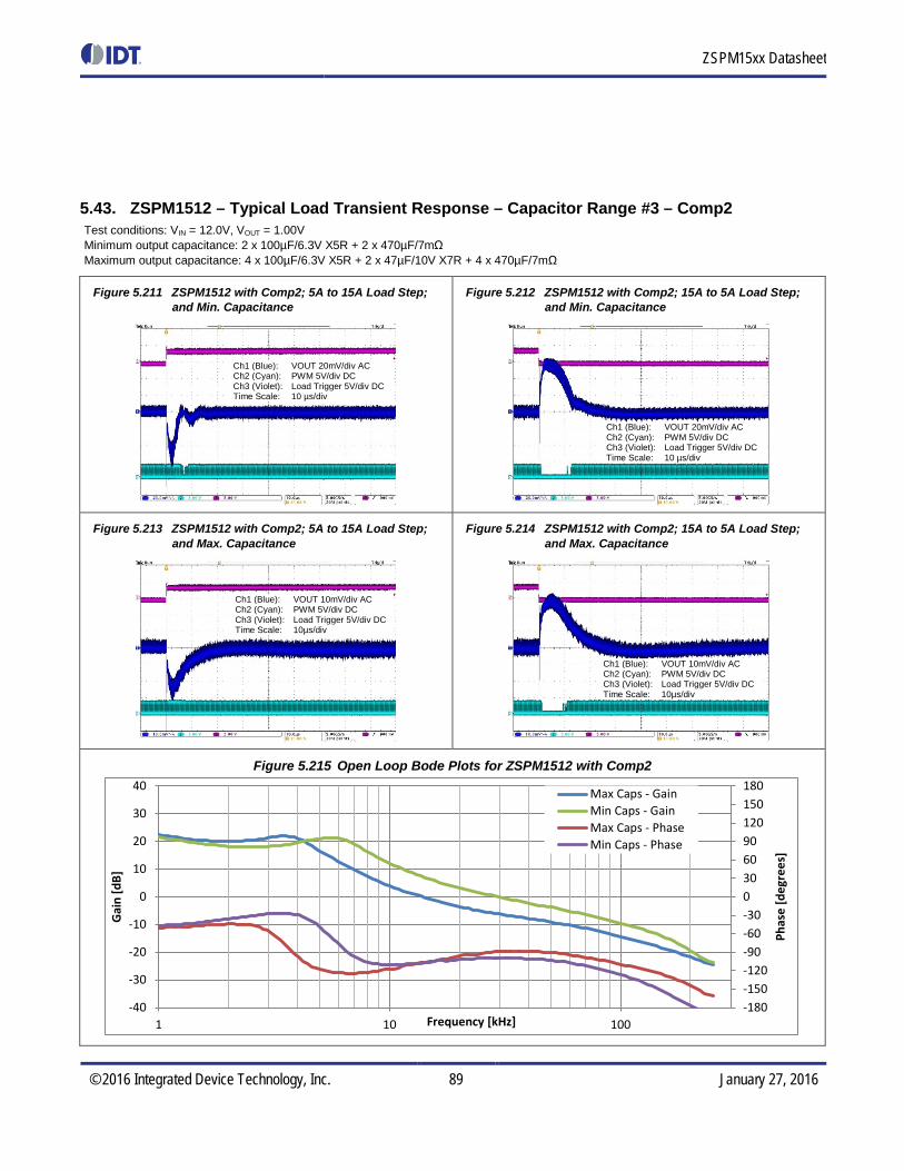
ZSPM15xx Datasheet
© 2016 Integrated Device Technology, Inc. 89 January 27, 2016
5.43. ZSPM1512 – Typical Load Transient Response – Capacitor Range #3 – Comp2 Test conditions: VIN = 12.0V, VOUT = 1.00V Minimum output capacitance: 2 x 100µF/6.3V X5R + 2 x 470µF/7mΩ Maximum output capacitance: 4 x 100µF/6.3V X5R + 2 x 47µF/10V X7R + 4 x 470µF/7mΩ
Figure 5.211 ZSPM1512 with Comp2; 5A to 15A Load Step; and Min. Capacitance
Figure 5.212 ZSPM1512 with Comp2; 15A to 5A Load Step; and Min. Capacitance
Figure 5.213 ZSPM1512 with Comp2; 5A to 15A Load Step; and Max. Capacitance
Figure 5.214 ZSPM1512 with Comp2; 15A to 5A Load Step; and Max. Capacitance
Figure 5.215 Open Loop Bode Plots for ZSPM1512 with Comp2
-180-150-120-90-60-300306090120150180
-40
-30
-20
-10
0
10
20
30
40
1 10 100
Phas
e [d
egre
es]
Gai
n [d
B]
Frequency [kHz]
Max Caps - GainMin Caps - GainMax Caps - PhaseMin Caps - Phase
Ch1 (Blue): VOUT 20mV/div AC Ch2 (Cyan): PWM 5V/div DC Ch3 (Violet): Load Trigger 5V/div DC Time Scale: 10 µs/div
Ch1 (Blue): VOUT 20mV/div AC Ch2 (Cyan): PWM 5V/div DC Ch3 (Violet): Load Trigger 5V/div DC Time Scale: 10 µs/div
Ch1 (Blue): VOUT 10mV/div AC Ch2 (Cyan): PWM 5V/div DC Ch3 (Violet): Load Trigger 5V/div DC Time Scale: 10µs/div
Ch1 (Blue): VOUT 10mV/div AC Ch2 (Cyan): PWM 5V/div DC Ch3 (Violet): Load Trigger 5V/div DC Time Scale: 10µs/div
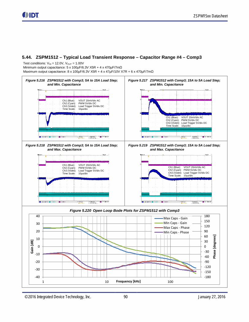
ZSPM15xx Datasheet
© 2016 Integrated Device Technology, Inc. 90 January 27, 2016
5.44. ZSPM1512 – Typical Load Transient Response – Capacitor Range #4 – Comp3 Test conditions: VIN = 12.0V, VOUT = 1.00V Minimum output capacitance: 5 x 100µF/6.3V X5R + 4 x 470µF/7mΩ Maximum output capacitance: 8 x 100µF/6.3V X5R + 4 x 47µF/10V X7R + 6 x 470µF/7mΩ
Figure 5.216 ZSPM1512 with Comp3; 5A to 15A Load Step; and Min. Capacitance
Figure 5.217 ZSPM1512 with Comp3; 15A to 5A Load Step; and Min. Capacitance
Figure 5.218 ZSPM1512 with Comp3; 5A to 15A Load Step; and Max. Capacitance
Figure 5.219 ZSPM1512 with Comp3; 15A to 5A Load Step; and Max. Capacitance
Figure 5.220 Open Loop Bode Plots for ZSPM1512 with Comp3
-180-150-120-90-60-300306090120150180
-40
-30
-20
-10
0
10
20
30
40
1 10 100
Phas
e [d
egre
es]
Gai
n [d
B]
Frequency [kHz]
Max Caps - GainMin Caps - GainMax Caps - PhaseMin Caps - Phase
Ch1 (Blue): VOUT 20mV/div AC Ch2 (Cyan): PWM 5V/div DC Ch3 (Violet): Load Trigger 5V/div DC Time Scale: 10µs/div
Ch1 (Blue): VOUT 20mV/div AC Ch2 (Cyan): PWM 5V/div DC Ch3 (Violet): Load Trigger 5V/div DC Time Scale: 10µs/div
Ch1 (Blue): VOUT 20mV/div AC Ch2 (Cyan): PWM 5V/div DC Ch3 (Violet): Load Trigger 5V/div DC Time Scale: 10µs/div
Ch1 (Blue): VOUT 20mV/div AC Ch2 (Cyan): PWM 5V/div DC Ch3 (Violet): Load Trigger 5V/div DC Time Scale: 10µs/div

ZSPM15xx Datasheet
© 2016 Integrated Device Technology, Inc. 91 January 27, 2016
5.45. ZSPM1513 – Typical Load Transient Response – Capacitor Range #1 – Comp0 Test conditions: VIN = 12.0V, VOUT = 1.20V Minimum output capacitance: 2 x 100µF/6.3V X5R Maximum output capacitance: 4 x 100µF/6.3V X5R + 2 x 47µF/10V X7R
Figure 5.221 ZSPM1513 with Comp0; 5A to 15A Load Step; and Min. Capacitance
Figure 5.222 ZSPM1513 with Comp0; 15A to 5A Load Step; and Min. Capacitance
Figure 5.223 ZSPM1513 with Comp0; 5A to 15A Load Step; and Max. Capacitance
Figure 5.224 ZSPM1513 with Comp0; 15A to 5A Load Step; and Max. Capacitance
Figure 5.225 Open Loop Bode Plots for ZSPM1513 with Comp0
-180-150-120-90-60-300306090120150180
-40
-30
-20
-10
0
10
20
30
40
1 10 100
Phas
e [d
egre
es]
Gai
n [d
B]
Frequency [kHz]
Max Caps - GainMin Caps - GainMax Caps - PhaseMin Caps - Phase
Ch1 (Blue): VOUT 100mV/div AC Ch2 (Cyan): PWM 5V/div DC Ch3 (Violet): Load Trigger 5V/div DC Time Scale: 10µs/div
Ch1 (Blue): VOUT 50mV/div AC Ch2 (Cyan): PWM 5V/div DC Ch3 (Violet): Load Trigger 5V/div DC Time Scale: 10µs/div
Ch1 (Blue): VOUT 100mV/div AC Ch2 (Cyan): PWM 5V/div DC Ch3 (Violet): Load Trigger 5V/div DC Time Scale: 10µs/div
Ch1 (Blue): VOUT 50mV/div AC Ch2 (Cyan): PWM 5V/div DC Ch3 (Violet): Load Trigger 5V/div DC Time Scale: 10µs/div

ZSPM15xx Datasheet
© 2016 Integrated Device Technology, Inc. 92 January 27, 2016
5.46. ZSPM1513 – Typical Load Transient Response – Capacitor Range #2 – Comp1 Test conditions: VIN = 12.0V, VOUT = 1.20V Minimum output capacitance: 5 x 100µF/6.3V X5R Maximum output capacitance: 8 x 100µF/6.3V X5R + 4 x 47µF/10V X7R
Figure 5.226 ZSPM1513 with Comp1; 5A to 15A Load Step; and Min. Capacitance
Figure 5.227 ZSPM1513 with Comp1; 15A to 5A Load Step; and Min. Capacitance
Figure 5.228 ZSPM1513 with Comp1; 5 to 15A Load Step; and Max. Capacitance
Figure 5.229 ZSPM1513 with Comp1; 15 to 5A Load Step; and Max. Capacitance
Figure 5.230 Open Loop Bode Plots for ZSPM1513 with Comp1
-180-150-120-90-60-300306090120150180
-40
-30
-20
-10
0
10
20
30
40
1 10 100
Phas
e [d
egre
es]
Gai
n [d
B]
Frequency [kHz]
Max Caps - GainMin Caps - GainMax Caps - PhaseMin Caps - Phase
Ch1 (Blue): VOUT 100mV/div AC Ch2 (Cyan): PWM 5V/div DC Ch3 (Violet): Load Trigger 5V/div DC Time Scale: 10µs/div
Ch1 (Blue): VOUT 50mV/div AC Ch2 (Cyan): PWM 5V/div DC Ch3 (Violet): Load Trigger 5V/div DC Time Scale: 10µs/div
Ch1 (Blue): VOUT 100mV/div AC Ch2 (Cyan): PWM 5V/div DC Ch3 (Violet): Load Trigger 5V/div DC Time Scale: 10µs/div
Ch1 (Blue): VOUT 50mV/div AC Ch2 (Cyan): PWM 5V/div DC Ch3 (Violet): Load Trigger 5V/div DC Time Scale: 10µs/div

ZSPM15xx Datasheet
© 2016 Integrated Device Technology, Inc. 93 January 27, 2016
5.47. ZSPM1513 – Typical Load Transient Response – Capacitor Range #3 – Comp2 Test conditions: VIN = 12.0V, VOUT = 1.20V Minimum output capacitance: 2 x 100µF/6.3V X5R + 2 x 470µF/7mΩ Maximum output capacitance: 4 x 100µF/6.3V X5R + 2 x 47µF/10V X7R + 4 x 470µF/7mΩ
Figure 5.231 ZSPM1513 with Comp2; 5A to 15A Load Step; and Min. Capacitance
Figure 5.232 ZSPM1513 with Comp2; 15A to 5A Load Step; and Min. Capacitance
Figure 5.233 ZSPM1513 with Comp2; 5A to 15A Load Step; and Max. Capacitance
Figure 5.234 ZSPM1513 with Comp2; 15A to 5A Load Step; and Max. Capacitance
Figure 5.235 Open Loop Bode Plots for ZSPM1513 with Comp2
-180-150-120-90-60-300306090120150180
-40
-30
-20
-10
0
10
20
30
40
1 10 100
Phas
e [d
egre
es]
Gai
n [d
B]
Frequency [kHz]
Max Caps - GainMin Caps - GainMax Caps - PhaseMin Caps - Phase
Ch1 (Blue): VOUT 10mV/div AC Ch2 (Cyan): PWM 5V/div DC Ch3 (Violet): Load Trigger 5V/div DC Time Scale: 10µs/div
Ch1 (Blue): VOUT 20mV/div AC Ch2 (Cyan): PWM 5V/div DC Ch3 (Violet): Load Trigger 5V/div DC Time Scale: 10µs/div
Ch1 (Blue): VOUT 10mV/div AC Ch2 (Cyan): PWM 5V/div DC Ch3 (Violet): Load Trigger 5V/div DC Time Scale: 10µs/div
Ch1 (Blue): VOUT 20mV/div AC Ch2 (Cyan): PWM 5V/div DC Ch3 (Violet): Load Trigger 5V/div DC Time Scale: 10µs/div
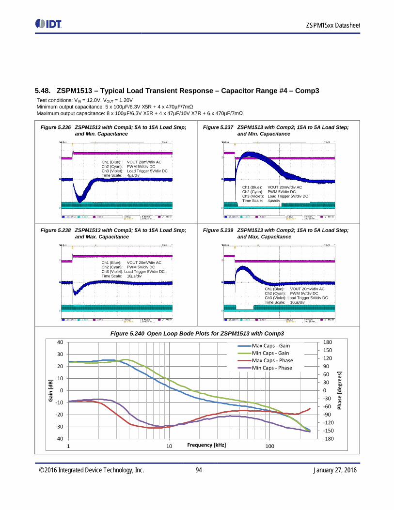
ZSPM15xx Datasheet
© 2016 Integrated Device Technology, Inc. 94 January 27, 2016
5.48. ZSPM1513 – Typical Load Transient Response – Capacitor Range #4 – Comp3 Test conditions: VIN = 12.0V, VOUT = 1.20V Minimum output capacitance: 5 x 100µF/6.3V X5R + 4 x 470µF/7mΩ Maximum output capacitance: 8 x 100µF/6.3V X5R + 4 x 47µF/10V X7R + 6 x 470µF/7mΩ
Figure 5.236 ZSPM1513 with Comp3; 5A to 15A Load Step; and Min. Capacitance
Figure 5.237 ZSPM1513 with Comp3; 15A to 5A Load Step; and Min. Capacitance
Figure 5.238 ZSPM1513 with Comp3; 5A to 15A Load Step; and Max. Capacitance
Figure 5.239 ZSPM1513 with Comp3; 15A to 5A Load Step; and Max. Capacitance
Figure 5.240 Open Loop Bode Plots for ZSPM1513 with Comp3
-180-150-120-90-60-300306090120150180
-40
-30
-20
-10
0
10
20
30
40
1 10 100
Phas
e [d
egre
es]
Gai
n [d
B]
Frequency [kHz]
Max Caps - GainMin Caps - GainMax Caps - PhaseMin Caps - Phase
Ch1 (Blue): VOUT 20mV/div AC Ch2 (Cyan): PWM 5V/div DC Ch3 (Violet): Load Trigger 5V/div DC Time Scale: 4µs/div
Ch1 (Blue): VOUT 20mV/div AC Ch2 (Cyan): PWM 5V/div DC Ch3 (Violet): Load Trigger 5V/div DC Time Scale: 10µs/div
Ch1 (Blue): VOUT 20mV/div AC Ch2 (Cyan): PWM 5V/div DC Ch3 (Violet): Load Trigger 5V/div DC Time Scale: 4µs/div
Ch1 (Blue): VOUT 20mV/div AC Ch2 (Cyan): PWM 5V/div DC Ch3 (Violet): Load Trigger 5V/div DC Time Scale: 10µs/div

ZSPM15xx Datasheet
© 2016 Integrated Device Technology, Inc. 95 January 27, 2016
5.49. Typical Efficiency Curves – ZSPM1502 with ZSPM9000, ZSPM9015, and ZSPM9060 DrMOS The following graph shows typical efficiency curves for the ZSPM1502 with three different IDT DrMOS power stage options: the ZSPM9000, ZSPM9015, and ZSPM9060. (Note: The ZSPM1502 is also compatible with the ZSPM9010, which is not shown.)
Figure 5.241 Typical Efficiency Curves: ZSPM1502 with ZSPM9000, ZSPM9015, and ZSPM9060 DrMOS (VIN= 12V; Vout = 1.0V)
Effic
ienc
y (%
)
Iout (A)
75.00%
76.00%
77.00%
78.00%
79.00%
80.00%
81.00%
82.00%
83.00%
84.00%
85.00%
86.00%
87.00%
88.00%
0 5 10 15 20 25 30 35 40 45
VIN = 12V Vout = 1.0V
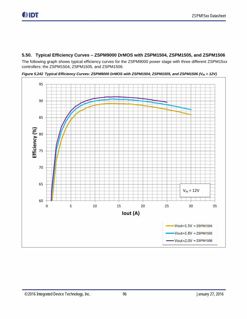
ZSPM15xx Datasheet
© 2016 Integrated Device Technology, Inc. 96 January 27, 2016
5.50. Typical Efficiency Curves – ZSPM9000 DrMOS with ZSPM1504, ZSPM1505, and ZSPM1506 The following graph shows typical efficiency curves for the ZSPM9000 power stage with three different ZSPM15xx controllers: the ZSPM1504, ZSPM1505, and ZSPM1506.
Figure 5.242 Typical Efficiency Curves: ZSPM9000 DrMOS with ZSPM1504, ZSPM1505, and ZSPM1506 (VIN = 12V)
60
65
70
75
80
85
90
95
0 5 10 15 20 25 30 35
Effic
ienc
y (%
)
Iout (A)
VIN = 12V

ZSPM15xx Datasheet
© 2016 Integrated Device Technology, Inc. 97 January 27, 2016
5.51. Typical Efficiency Curves – ZSPM9000 and ZSPM9060 DrMOS with ZSPM1508 and ZSPM1509
The following graph shows typical efficiency curves for the ZSPM9000 and ZSPM9060 power stages with two different ZSPM15xx controllers: the ZSPM1508 and ZSPM1509.
Figure 5.243 Typical Efficiency Curves: ZSPM9000 and ZSPM9060 DrMOS with ZSPM1508 and ZSPM1509
60
65
70
75
80
85
90
95
100
0 2 4 6 8 10 12 14 16
Effic
ienc
y (%
)
Iout (A)
VIN = 12V
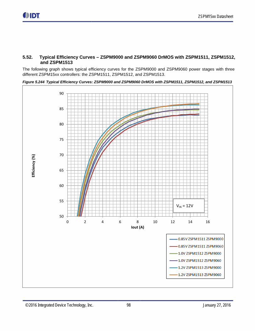
ZSPM15xx Datasheet
© 2016 Integrated Device Technology, Inc. 98 January 27, 2016
5.52. Typical Efficiency Curves – ZSPM9000 and ZSPM9060 DrMOS with ZSPM1511, ZSPM1512, and ZSPM1513
The following graph shows typical efficiency curves for the ZSPM9000 and ZSPM9060 power stages with three different ZSPM15xx controllers: the ZSPM1511, ZSPM1512, and ZSPM1513.
Figure 5.244 Typical Efficiency Curves: ZSPM9000 and ZSPM9060 DrMOS with ZSPM1511, ZSPM1512, and ZSPM1513
50
55
60
65
70
75
80
85
90
0 2 4 6 8 10 12 14 16
Effic
ienc
y (%
)
Iout (A)
VIN = 12V

ZSPM15xx Datasheet
© 2016 Integrated Device Technology, Inc. 99 January 27, 2016
6 Mechanical Specifications Based on JEDEC MO-220. All dimensions are in millimeters.
Figure 6.1 24-Pin QFN Package Drawing
Dimensions Minimum (mm) Maximum (mm)
A 0.8 0.90
A1 0.00 0.05
b 0.18 0.30
e 0.5 nominal
HD 3.90 4.1
HE 3.90 4.1
L 0.35 0.45

ZSPM15xx Datasheet
© 2016 Integrated Device Technology, Inc. 100 January 27, 2016
7 Ordering Information Product Code Description Package
ZSPM1501ZA1W0 ZSPM1501 lead-free QFN24; output voltage: 0.85V; inductance: 330nH; temperature: -40°C to +125°C Reel
ZSPM1502ZA1W0 ZSPM1502 lead-free QFN24; output voltage: 1.00V; inductance: 330nH; temperature: -40°C to +125°C Reel
ZSPM1503ZA1W0 ZSPM1503 lead-free QFN24; output voltage: 1.20V; inductance: 330nH; temperature: -40°C to +125°C Reel
ZSPM1504ZA1W0 ZSPM1504 lead-free QFN24; output voltage: 1.50V; inductance: 470nH; temperature: -40°C to +125°C Reel
ZSPM1505ZA1W0 ZSPM1505 lead-free QFN24; output voltage: 1.80V; inductance: 470nH; temperature: -40°C to +125°C Reel
ZSPM1506ZA1W0 ZSPM1506 lead-free QFN24; output voltage: 2.00V; inductance: 470nH; temperature: -40°C to +125°C Reel
ZSPM1507ZA1W0 ZSPM1507 lead-free QFN24; output voltage: 2.50V; inductance: 1000nH; temperature: -40°C to +125°C Reel
ZSPM1508ZA1W0 ZSPM1508 lead-free QFN24; output voltage: 3.30V; inductance: 2200nH; temperature: -40°C to +125°C Reel
ZSPM1509ZA1W0 ZSPM1509 lead-free QFN24; output voltage: 5.00V; inductance: 2200nH; temperature: -40°C to +125°C Reel
ZSPM1511ZA1W0 ZSPM1511 lead-free QFN24; output voltage: 0.85V; inductance: 680nH; temperature: -40°C to +125°C Reel
ZSPM1512ZA1W0 ZSPM1512 lead-free QFN24; output voltage: 1.00V; inductance: 680nH; temperature: -40°C to +125°C Reel
ZSPM1513ZA1W0 ZSPM1513 lead-free QFN24; output voltage: 1.20V; inductance: 680nH; temperature: -40°C to +125°C Reel
8 Related Documents
Document
ZSPM15xx Family Feature Sheet
ZSPM15XX-KIT01 Kit Description
Visit the ZSPM15xx product page www.IDT.com/ZSPM15xx or contact your nearest sales office for the latest version of these documents.

ZSPM15xx Datasheet
© 2016 Integrated Device Technology, Inc. 101 January 27, 2016
9 Glossary Term Description
DCR Equivalent DC Resistance
DNP Do Not Place (Component)
DPWM Digital Pulse-Width Modulator
DSP Digital Signal Processing
FPGA Field-Programmable Gate Array
HKADC Housekeeping Analog-To-Digital Converter
OCP Over-Current Protection
OT Over-Temperature
OV Over-Voltage
PID Proportional/Integral/Derivative
SLC State-Law Control™
SPM Smart Power Management
10 Document Revision History Revision Date Description
2.00 November 24, 2014 First release of full revision.
2.10 March 9, 2015 Addition of ZSPM1507, ZSPM1508, and ZSPM1509 to family of products.
2.20 April 27, 2015 Addition of ZSPM1511, ZSPM1512, and ZSPM1513 to family of products. Removal of references to Sub-cycle Response (SCR) as this is not activated in the ZSPM15xx. Addition of Table 4.10, Table 4.11, and Table 4.12 for CONFIG 1 settings for the ZSPM1507, ZSPM1508, and ZSPM1509 respectively. Correction of C9 to C10 in section 4.5.
January 27, 2016 Changed to IDT branding.
Corporate Headquarters 6024 Silver Creek Valley Road San Jose, CA 95138 www.IDT.com
Sales 1-800-345-7015 or 408-284-8200 Fax: 408-284-2775 www.IDT.com/go/sales
Tech Support www.IDT.com/go/support
DISCLAIMER Integrated Device Technology, Inc. (IDT) reserves the right to modify the products and/or specifications described herein at any time, without notice, at IDT's sole discretion. Performance specifications and operating parameters of the described products are determined in an independent state and are not guaranteed to perform the same way when installed in customer products. The information contained herein is provided without representation or warranty of any kind, whether express or implied, including, but not limited to, the suitability of IDT's products for any particular purpose, an implied warranty of merchantability, or non-infringement of the intellectual property rights of others. This document is presented only as a guide and does not convey any license under intellectual property rights of IDT or any third parties. IDT's products are not intended for use in applications involving extreme environmental conditions or in life support systems or similar devices where the failure or malfunction of an IDT product can be reasonably expected to significantly affect the health or safety of users. Anyone using an IDT product in such a manner does so at their own risk, absent an express, written agreement by IDT. Integrated Device Technology, IDT and the IDT logo are trademarks or registered trademarks of IDT and its subsidiaries in the United States and other countries. Other trademarks used herein are the property of IDT or their respective third party owners. For datasheet type definitions and a glossary of common terms, visit www.idt.com/go/glossary. All contents of this document are copyright of Integrated Device Technology, Inc. All rights reserved.

Mouser Electronics
Authorized Distributor
Click to View Pricing, Inventory, Delivery & Lifecycle Information: IDT (Integrated Device Technology):
ZSPM1508ZA1W0 ZSPM1503ZA1W0 ZSPM1502ZA1W0 ZSPM1506ZA1W0 ZSPM1501ZA1W0
ZSPM1509ZA1W0 ZSPM1504ZA1W0 ZSPM1511ZA1W0 ZSPM1507ZA1W0 ZSPM1512ZA1W0 ZSPM1513ZA1W0
ZSPM1505ZA1W0