
TriBoard Manual TC3X7 V2 - Infineon Technologies
60
User Manual Please read the Important Notice and Warnings at the end of this document V2.3 www.infineon.com TriBoard TC3X7 TH V2.0(1) and TriBoard TC3X7 V2.0 2019-09 TriBoard TC3X7 TriBoard Manual TC3X7 Hardware: TriBoard TC3X7 TH V2.0(1) and TriBoard TC3X7 V2.0 About this document Scope and purpose The User Manual provide information about using, configuration and connecting the TriBoard with Infineon AURIX™ TC3X7 device. The manual provide information for different hardware types. There exist different hardware with Through Hole socket (TriBoard TC3X7 TH) and soldered devices (TriBoard TC3X7). The schematic is identically for the all boards if not other mentioned in chapter schematic. The placing on the boards is slightly different around the TC3X7 itself dependent of the space (socket need more space and has through hole), but the most components are on the same location. All figures are valid for each board if not differently mentioned. Intended audience Design, verfication, test and software engineers will use this document to get an understanding of the functionality and connections of the TriBoard.
Transcript of TriBoard Manual TC3X7 V2 - Infineon Technologies

User Manual Please read the Important Notice and Warnings at the end of this document V2.3www.infineon.com TriBoard TC3X7 TH V2.0(1) and TriBoard TC3X7 V2.0 2019-09
TriBoard TC3X7
TriBoard Manual TC3X7Hardware: Tr iBoard TC3X7 TH V2.0(1) and TriBoard TC3X7 V2.0
About this document
Scope and purpose
The User Manual provide information about using, configuration and connecting the TriBoard with InfineonAURIX™ TC3X7 device. The manual provide information for different hardware types. There exist differenthardware with Through Hole socket (TriBoard TC3X7 TH) and soldered devices (TriBoard TC3X7). The schematicis identically for the all boards if not other mentioned in chapter schematic. The placing on the boards is slightlydifferent around the TC3X7 itself dependent of the space (socket need more space and has through hole), but themost components are on the same location. All figures are valid for each board if not differently mentioned.
Intended audience
Design, verfication, test and software engineers will use this document to get an understanding of thefunctionality and connections of the TriBoard.
User Manual TOC-2 V2.3 TriBoard TC3X7 TH V2.0(1) and TriBoard TC3X7 V2.0 2019-09
TriBoard Manual TC3X7Hardware: TriBoard TC3X7 TH V2.0(1) and TriBoard TC3X7 V2.0
Table of Contents
About this document . . . . . . . . . . . . . . . . . . . . . . . . . . . . . . . . . . . . . . . . . . . . . . . . . . . . . . . . . . . . . . . . . Preface-1
Table of Contents . . . . . . . . . . . . . . . . . . . . . . . . . . . . . . . . . . . . . . . . . . . . . . . . . . . . . . . . . . . . . . . . . . . . . . . TOC-2
1 Introduction . . . . . . . . . . . . . . . . . . . . . . . . . . . . . . . . . . . . . . . . . . . . . . . . . . . . . . . . . . . . . . . . . . . . . . . . . . . . . . 1-1
2 Features . . . . . . . . . . . . . . . . . . . . . . . . . . . . . . . . . . . . . . . . . . . . . . . . . . . . . . . . . . . . . . . . . . . . . . . . . . . . . . . . . . 2-12.1 Summary of Features . . . . . . . . . . . . . . . . . . . . . . . . . . . . . . . . . . . . . . . . . . . . . . . . . . . . . . . . . . . . . . . . . . . . . . . 2-12.2 Block Diagram . . . . . . . . . . . . . . . . . . . . . . . . . . . . . . . . . . . . . . . . . . . . . . . . . . . . . . . . . . . . . . . . . . . . . . . . . . . . . 2-32.3 Placement . . . . . . . . . . . . . . . . . . . . . . . . . . . . . . . . . . . . . . . . . . . . . . . . . . . . . . . . . . . . . . . . . . . . . . . . . . . . . . . . . 2-4
3 TriBoard Information . . . . . . . . . . . . . . . . . . . . . . . . . . . . . . . . . . . . . . . . . . . . . . . . . . . . . . . . . . . . . . . . . . . . . . 3-13.1 Soldered board . . . . . . . . . . . . . . . . . . . . . . . . . . . . . . . . . . . . . . . . . . . . . . . . . . . . . . . . . . . . . . . . . . . . . . . . . . . . 3-13.2 Socketed board . . . . . . . . . . . . . . . . . . . . . . . . . . . . . . . . . . . . . . . . . . . . . . . . . . . . . . . . . . . . . . . . . . . . . . . . . . . . 3-13.2.1 Usable devices . . . . . . . . . . . . . . . . . . . . . . . . . . . . . . . . . . . . . . . . . . . . . . . . . . . . . . . . . . . . . . . . . . . . . . . . . . . 3-23.2.2 Restricted usable devices . . . . . . . . . . . . . . . . . . . . . . . . . . . . . . . . . . . . . . . . . . . . . . . . . . . . . . . . . . . . . . . . . . 3-23.3 Power Supply . . . . . . . . . . . . . . . . . . . . . . . . . . . . . . . . . . . . . . . . . . . . . . . . . . . . . . . . . . . . . . . . . . . . . . . . . . . . . . 3-53.3.1 Failsafe handling . . . . . . . . . . . . . . . . . . . . . . . . . . . . . . . . . . . . . . . . . . . . . . . . . . . . . . . . . . . . . . . . . . . . . . . . . 3-53.4 LEDs . . . . . . . . . . . . . . . . . . . . . . . . . . . . . . . . . . . . . . . . . . . . . . . . . . . . . . . . . . . . . . . . . . . . . . . . . . . . . . . . . . . . . . 3-63.5 Clock . . . . . . . . . . . . . . . . . . . . . . . . . . . . . . . . . . . . . . . . . . . . . . . . . . . . . . . . . . . . . . . . . . . . . . . . . . . . . . . . . . . . . . 3-63.6 USB Connector . . . . . . . . . . . . . . . . . . . . . . . . . . . . . . . . . . . . . . . . . . . . . . . . . . . . . . . . . . . . . . . . . . . . . . . . . . . . . 3-63.6.1 Serial Connection to PC . . . . . . . . . . . . . . . . . . . . . . . . . . . . . . . . . . . . . . . . . . . . . . . . . . . . . . . . . . . . . . . . . . . 3-73.6.2 miniWiggler JDS . . . . . . . . . . . . . . . . . . . . . . . . . . . . . . . . . . . . . . . . . . . . . . . . . . . . . . . . . . . . . . . . . . . . . . . . . . 3-73.7 FlexRay™ (E-RAY) . . . . . . . . . . . . . . . . . . . . . . . . . . . . . . . . . . . . . . . . . . . . . . . . . . . . . . . . . . . . . . . . . . . . . . . . . . . 3-83.8 Serial Eeprom . . . . . . . . . . . . . . . . . . . . . . . . . . . . . . . . . . . . . . . . . . . . . . . . . . . . . . . . . . . . . . . . . . . . . . . . . . . . . . 3-83.9 MultiCAN . . . . . . . . . . . . . . . . . . . . . . . . . . . . . . . . . . . . . . . . . . . . . . . . . . . . . . . . . . . . . . . . . . . . . . . . . . . . . . . . . . 3-83.10 LIN . . . . . . . . . . . . . . . . . . . . . . . . . . . . . . . . . . . . . . . . . . . . . . . . . . . . . . . . . . . . . . . . . . . . . . . . . . . . . . . . . . . . . . . . 3-93.11 Ethernet . . . . . . . . . . . . . . . . . . . . . . . . . . . . . . . . . . . . . . . . . . . . . . . . . . . . . . . . . . . . . . . . . . . . . . . . . . . . . . . . . . . 3-93.12 HSCT (optional) . . . . . . . . . . . . . . . . . . . . . . . . . . . . . . . . . . . . . . . . . . . . . . . . . . . . . . . . . . . . . . . . . . . . . . . . . . 3-103.12.1 High speed with HSCT . . . . . . . . . . . . . . . . . . . . . . . . . . . . . . . . . . . . . . . . . . . . . . . . . . . . . . . . . . . . . . . . . . . 3-103.13 ADC . . . . . . . . . . . . . . . . . . . . . . . . . . . . . . . . . . . . . . . . . . . . . . . . . . . . . . . . . . . . . . . . . . . . . . . . . . . . . . . . . . . . . 3-113.14 Other peripherals . . . . . . . . . . . . . . . . . . . . . . . . . . . . . . . . . . . . . . . . . . . . . . . . . . . . . . . . . . . . . . . . . . . . . . . . 3-133.15 Toggle LED’s . . . . . . . . . . . . . . . . . . . . . . . . . . . . . . . . . . . . . . . . . . . . . . . . . . . . . . . . . . . . . . . . . . . . . . . . . . . . . 3-133.16 Buttons . . . . . . . . . . . . . . . . . . . . . . . . . . . . . . . . . . . . . . . . . . . . . . . . . . . . . . . . . . . . . . . . . . . . . . . . . . . . . . . . . 3-133.17 Debug System . . . . . . . . . . . . . . . . . . . . . . . . . . . . . . . . . . . . . . . . . . . . . . . . . . . . . . . . . . . . . . . . . . . . . . . . . . . 3-133.17.1 OCDS1 . . . . . . . . . . . . . . . . . . . . . . . . . . . . . . . . . . . . . . . . . . . . . . . . . . . . . . . . . . . . . . . . . . . . . . . . . . . . . . . . . 3-133.17.2 DAP . . . . . . . . . . . . . . . . . . . . . . . . . . . . . . . . . . . . . . . . . . . . . . . . . . . . . . . . . . . . . . . . . . . . . . . . . . . . . . . . . . . 3-133.17.3 DAPE (only Emulation Device) . . . . . . . . . . . . . . . . . . . . . . . . . . . . . . . . . . . . . . . . . . . . . . . . . . . . . . . . . . . . 3-133.17.4 DAP_SCR . . . . . . . . . . . . . . . . . . . . . . . . . . . . . . . . . . . . . . . . . . . . . . . . . . . . . . . . . . . . . . . . . . . . . . . . . . . . . . 3-143.17.5 High speed with DAP/DAPE . . . . . . . . . . . . . . . . . . . . . . . . . . . . . . . . . . . . . . . . . . . . . . . . . . . . . . . . . . . . . . 3-143.17.6 AGBT (optional) . . . . . . . . . . . . . . . . . . . . . . . . . . . . . . . . . . . . . . . . . . . . . . . . . . . . . . . . . . . . . . . . . . . . . . . . 3-153.17.7 ETK connector (optional) . . . . . . . . . . . . . . . . . . . . . . . . . . . . . . . . . . . . . . . . . . . . . . . . . . . . . . . . . . . . . . . . 3-153.17.8 EmW Power (optional) . . . . . . . . . . . . . . . . . . . . . . . . . . . . . . . . . . . . . . . . . . . . . . . . . . . . . . . . . . . . . . . . . . 3-15
4 TriBoard Configuration . . . . . . . . . . . . . . . . . . . . . . . . . . . . . . . . . . . . . . . . . . . . . . . . . . . . . . . . . . . . . . . . . . . . 4-14.1 HW Boot Configuration . . . . . . . . . . . . . . . . . . . . . . . . . . . . . . . . . . . . . . . . . . . . . . . . . . . . . . . . . . . . . . . . . . . . . 4-14.1.1 Default Pad State . . . . . . . . . . . . . . . . . . . . . . . . . . . . . . . . . . . . . . . . . . . . . . . . . . . . . . . . . . . . . . . . . . . . . . . . . 4-14.1.2 Bootmode . . . . . . . . . . . . . . . . . . . . . . . . . . . . . . . . . . . . . . . . . . . . . . . . . . . . . . . . . . . . . . . . . . . . . . . . . . . . . . . 4-14.2 Assembly Options . . . . . . . . . . . . . . . . . . . . . . . . . . . . . . . . . . . . . . . . . . . . . . . . . . . . . . . . . . . . . . . . . . . . . . . . . . 4-24.2.1 General optional resistors . . . . . . . . . . . . . . . . . . . . . . . . . . . . . . . . . . . . . . . . . . . . . . . . . . . . . . . . . . . . . . . . . 4-24.2.2 Resistors for peripherals . . . . . . . . . . . . . . . . . . . . . . . . . . . . . . . . . . . . . . . . . . . . . . . . . . . . . . . . . . . . . . . . . . 4-4
Table of Contents

User Manual TOC-3 V2.3 TriBoard TC3X7 TH V2.0(1) and TriBoard TC3X7 V2.0 2019-09
TriBoard Manual TC3X7Hardware: TriBoard TC3X7 TH V2.0(1) and TriBoard TC3X7 V2.0
Table of Contents
5 Signal (on board used) Description . . . . . . . . . . . . . . . . . . . . . . . . . . . . . . . . . . . . . . . . . . . . . . . . . . . . . . . . . . 5-15.1 Power Signals . . . . . . . . . . . . . . . . . . . . . . . . . . . . . . . . . . . . . . . . . . . . . . . . . . . . . . . . . . . . . . . . . . . . . . . . . . . . . . 5-15.2 Reset Signals . . . . . . . . . . . . . . . . . . . . . . . . . . . . . . . . . . . . . . . . . . . . . . . . . . . . . . . . . . . . . . . . . . . . . . . . . . . . . . 5-15.3 Config Signals . . . . . . . . . . . . . . . . . . . . . . . . . . . . . . . . . . . . . . . . . . . . . . . . . . . . . . . . . . . . . . . . . . . . . . . . . . . . . . 5-25.4 Clock Signals . . . . . . . . . . . . . . . . . . . . . . . . . . . . . . . . . . . . . . . . . . . . . . . . . . . . . . . . . . . . . . . . . . . . . . . . . . . . . . 5-25.5 Debug Signals . . . . . . . . . . . . . . . . . . . . . . . . . . . . . . . . . . . . . . . . . . . . . . . . . . . . . . . . . . . . . . . . . . . . . . . . . . . . . . 5-25.6 Peripheral Signals . . . . . . . . . . . . . . . . . . . . . . . . . . . . . . . . . . . . . . . . . . . . . . . . . . . . . . . . . . . . . . . . . . . . . . . . . . 5-3
6 Connector Pin Assignment . . . . . . . . . . . . . . . . . . . . . . . . . . . . . . . . . . . . . . . . . . . . . . . . . . . . . . . . . . . . . . . . . 6-16.1 On Board only used signals . . . . . . . . . . . . . . . . . . . . . . . . . . . . . . . . . . . . . . . . . . . . . . . . . . . . . . . . . . . . . . . . . . 6-16.2 TC397/TC387/TC377/TC3E7 Connector / Top View . . . . . . . . . . . . . . . . . . . . . . . . . . . . . . . . . . . . . . . . . . . . . 6-26.3 TC367 Connector / Top View . . . . . . . . . . . . . . . . . . . . . . . . . . . . . . . . . . . . . . . . . . . . . . . . . . . . . . . . . . . . . . . . . 6-46.4 TC337/TC327 Connector / Top View . . . . . . . . . . . . . . . . . . . . . . . . . . . . . . . . . . . . . . . . . . . . . . . . . . . . . . . . . . 6-66.5 Power connector pinout . . . . . . . . . . . . . . . . . . . . . . . . . . . . . . . . . . . . . . . . . . . . . . . . . . . . . . . . . . . . . . . . . . . . 6-86.6 USB connector pinout . . . . . . . . . . . . . . . . . . . . . . . . . . . . . . . . . . . . . . . . . . . . . . . . . . . . . . . . . . . . . . . . . . . . . . 6-86.7 FlexRay™ (ERAY) connector pinout . . . . . . . . . . . . . . . . . . . . . . . . . . . . . . . . . . . . . . . . . . . . . . . . . . . . . . . . . . . 6-86.8 CAN connector pinout . . . . . . . . . . . . . . . . . . . . . . . . . . . . . . . . . . . . . . . . . . . . . . . . . . . . . . . . . . . . . . . . . . . . . . 6-86.9 LIN connector pinout . . . . . . . . . . . . . . . . . . . . . . . . . . . . . . . . . . . . . . . . . . . . . . . . . . . . . . . . . . . . . . . . . . . . . . . 6-96.10 HSCT connector pinout . . . . . . . . . . . . . . . . . . . . . . . . . . . . . . . . . . . . . . . . . . . . . . . . . . . . . . . . . . . . . . . . . . . . . 6-96.11 Ethernet connector pinout . . . . . . . . . . . . . . . . . . . . . . . . . . . . . . . . . . . . . . . . . . . . . . . . . . . . . . . . . . . . . . . . . . 6-96.12 OCDS1 connector pinout . . . . . . . . . . . . . . . . . . . . . . . . . . . . . . . . . . . . . . . . . . . . . . . . . . . . . . . . . . . . . . . . . . 6-106.13 DAP connector pinout . . . . . . . . . . . . . . . . . . . . . . . . . . . . . . . . . . . . . . . . . . . . . . . . . . . . . . . . . . . . . . . . . . . . 6-106.14 ETK connector pinout . . . . . . . . . . . . . . . . . . . . . . . . . . . . . . . . . . . . . . . . . . . . . . . . . . . . . . . . . . . . . . . . . . . . . 6-116.15 Ethernet miniWiggler power connector pinout . . . . . . . . . . . . . . . . . . . . . . . . . . . . . . . . . . . . . . . . . . . . . . 6-116.16 AGBT connector pinout . . . . . . . . . . . . . . . . . . . . . . . . . . . . . . . . . . . . . . . . . . . . . . . . . . . . . . . . . . . . . . . . . . . 6-12
7 Schematic and Layout . . . . . . . . . . . . . . . . . . . . . . . . . . . . . . . . . . . . . . . . . . . . . . . . . . . . . . . . . . . . . . . . . . . . . 7-17.1 Known problems . . . . . . . . . . . . . . . . . . . . . . . . . . . . . . . . . . . . . . . . . . . . . . . . . . . . . . . . . . . . . . . . . . . . . . . . . . . 7-17.1.1 Known problems on TriBoard TC3X7 TH V2.0(1) . . . . . . . . . . . . . . . . . . . . . . . . . . . . . . . . . . . . . . . . . . . . . . 7-17.1.2 Known problems on TriBoard TC3X7 V2.0 . . . . . . . . . . . . . . . . . . . . . . . . . . . . . . . . . . . . . . . . . . . . . . . . . . . 7-17.2 Schematic . . . . . . . . . . . . . . . . . . . . . . . . . . . . . . . . . . . . . . . . . . . . . . . . . . . . . . . . . . . . . . . . . . . . . . . . . . . . . . . . . 7-17.3 Layout . . . . . . . . . . . . . . . . . . . . . . . . . . . . . . . . . . . . . . . . . . . . . . . . . . . . . . . . . . . . . . . . . . . . . . . . . . . . . . . . . . . . 7-97.4 Layout with Dimensioning . . . . . . . . . . . . . . . . . . . . . . . . . . . . . . . . . . . . . . . . . . . . . . . . . . . . . . . . . . . . . . . . . 7-11
User Manual 1-1 V2.3 TriBoard TC3X7 TH V2.0(1) and TriBoard TC3X7 V2.0 2019-09
TriBoard Manual TC3X7Hardware: TriBoard TC3X7 TH V2.0(1) and TriBoard TC3X7 V2.0
Introduction
1 IntroductionWe congratulate you on your purchase of the TriCore Evaluation Board. This kit is a versatile tool, providing quickaccess to the capabilities of TriCore's powerful architecture.Applications can be developed easily. The Evaluation Board is equipped with a variety of memories andperipherals for connection to the environment. There is also an interface for the On Chip Debugging Features(OCDS1 and DAP). The Evaluation Board allows easily the development of TriCore applications with the corresponding tools.Subsequently, the applications can be downloaded and can be tested with the powerful debugger software.This TriBoard Hardware Manual familiarizes you with the TriCore Evaluation Board and guides you through theinitial configuration of the TriBoard. For detailed technical information about the TC3X7 (e.g. TC397, TC387, TC377, TC367, TC337, TC327, TC3E7)please refer to the User Manual of the used device.
User Manual 2-1 V2.3 TriBoard TC3X7 TH V2.0(1) and TriBoard TC3X7 V2.0 2019-09
TriBoard Manual TC3X7Hardware: TriBoard TC3X7 TH V2.0(1) and TriBoard TC3X7 V2.0
Features
2 Features
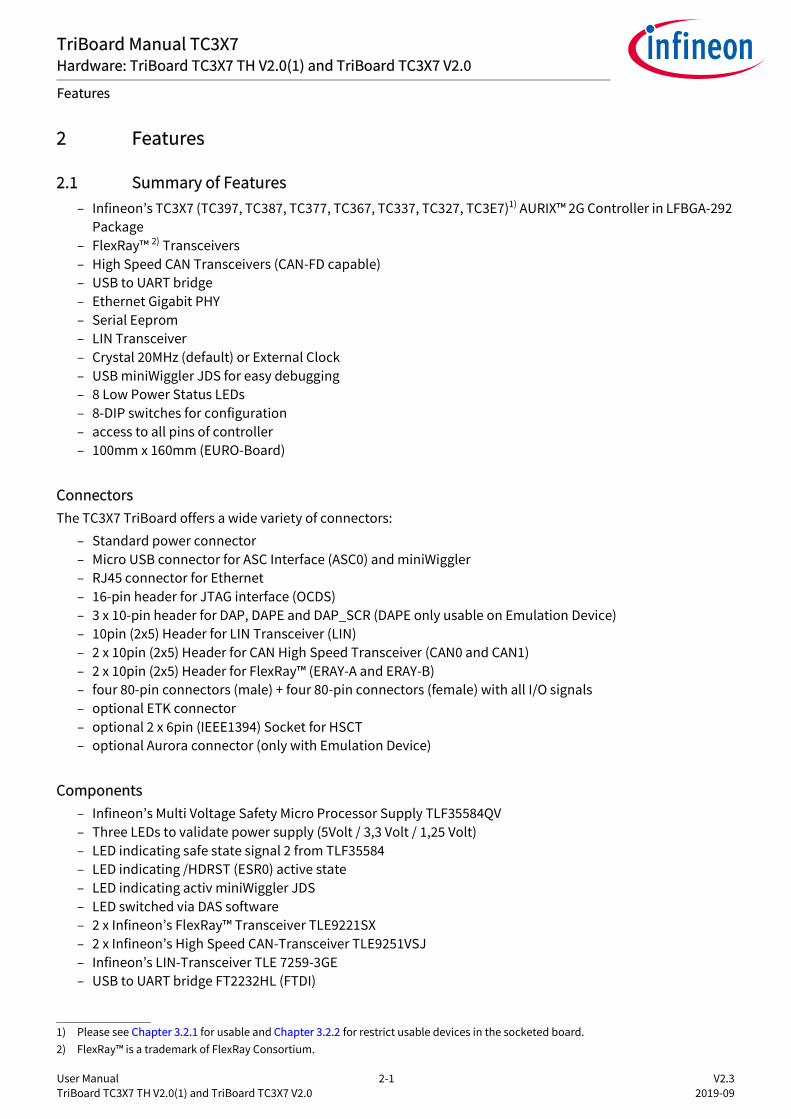
2.1 Summary of Features– Infineon’s TC3X7 (TC397, TC387, TC377, TC367, TC337, TC327, TC3E7)1) AURIX™ 2G Controller in LFBGA-292
Package– FlexRay™ 2) Transceivers– High Speed CAN Transceivers (CAN-FD capable)– USB to UART bridge– Ethernet Gigabit PHY– Serial Eeprom– LIN Transceiver– Crystal 20MHz (default) or External Clock– USB miniWiggler JDS for easy debugging– 8 Low Power Status LEDs– 8-DIP switches for configuration– access to all pins of controller– 100mm x 160mm (EURO-Board)
ConnectorsThe TC3X7 TriBoard offers a wide variety of connectors:
– Standard power connector– Micro USB connector for ASC Interface (ASC0) and miniWiggler– RJ45 connector for Ethernet– 16-pin header for JTAG interface (OCDS)– 3 x 10-pin header for DAP, DAPE and DAP_SCR (DAPE only usable on Emulation Device)– 10pin (2x5) Header for LIN Transceiver (LIN)– 2 x 10pin (2x5) Header for CAN High Speed Transceiver (CAN0 and CAN1)– 2 x 10pin (2x5) Header for FlexRay™ (ERAY-A and ERAY-B)– four 80-pin connectors (male) + four 80-pin connectors (female) with all I/O signals– optional ETK connector– optional 2 x 6pin (IEEE1394) Socket for HSCT– optional Aurora connector (only with Emulation Device)
Components– Infineon’s Multi Voltage Safety Micro Processor Supply TLF35584QV– Three LEDs to validate power supply (5Volt / 3,3 Volt / 1,25 Volt)– LED indicating safe state signal 2 from TLF35584– LED indicating /HDRST (ESR0) active state– LED indicating activ miniWiggler JDS– LED switched via DAS software– 2 x Infineon’s FlexRay™ Transceiver TLE9221SX– 2 x Infineon’s High Speed CAN-Transceiver TLE9251VSJ– Infineon’s LIN-Transceiver TLE 7259-3GE– USB to UART bridge FT2232HL (FTDI)
1) Please see Chapter 3.2.1 for usable and Chapter 3.2.2 for restrict usable devices in the socketed board.2) FlexRay™ is a trademark of FlexRay Consortium.

User Manual 2-2 V2.3 TriBoard TC3X7 TH V2.0(1) and TriBoard TC3X7 V2.0 2019-09
TriBoard Manual TC3X7Hardware: TriBoard TC3X7 TH V2.0(1) and TriBoard TC3X7 V2.0
Features
– Integrated 10/100/1000M Ethernet Precision Transceiver RTL8211FI-CG (Realtek)– 8 general purpose LEDs– 2K I2C Serial Eeprom with EUI-48™ 1) Node Identity (MICROCHIP)– Reset switch– Enable switch– Generic switch– 4-pin Dip switch
Zero Ohm BridgesZero Ohm resistors give the flexibility to configure the systems functionality.
1) EUI-48™ is trademarked by IEEE

User Manual 2-3 V2.3 TriBoard TC3X7 TH V2.0(1) and TriBoard TC3X7 V2.0 2019-09
TriBoard Manual TC3X7Hardware: TriBoard TC3X7 TH V2.0(1) and TriBoard TC3X7 V2.0
Features
2.2 Block Diagram
Figure 2-1 TriBoard Block Schematic
MicroUSB miniWiggler
OCDS1
USB
XTAL
FlexRay™ Transceiver
Transceiver
TxCAN0
TxCAN1
RxCAN0
RxCAN1
TC3X7(e.g.
TC397, TC387, TC377, TC367, TC337, TC327, TC3E7)TriCore
CPU
PLLCAN0
CAN1
ER
AY
BE
RAY
A
TX0
RX0
8 LED’s (P33.4 up to P33.7,
P20.11 up to P20.14)Serial EEPROM with EUI-48™
RGMII PHYTwisted Pair
RJ45
LIN LIN
Transceiver
TX1
RX1
I²C
WAKEUP
QSPI2
Multi Voltage Safety Micro Processor Supply
TLF35584QV
ENA
HS
CT1
optio
nalHSCT1 - TX/RX
HSCT0 - TX/RX
HSC
T0op
tiona
l

User Manual 2-4 V2.3 TriBoard TC3X7 TH V2.0(1) and TriBoard TC3X7 V2.0 2019-09
TriBoard Manual TC3X7Hardware: TriBoard TC3X7 TH V2.0(1) and TriBoard TC3X7 V2.0
Features
2.3 Placement
Figure 2-2 TriBoard TC3X7 (TH) V2.0(1) Placement
U201
X40
6
X202
X502
X403
S202
R5
01
C50
1
C502
L50
1
L502
U501
D508
U502
S502
X404
S501
X50
1
X401
D504 D507
D506
D505
D309D308D307D306D305D304D303D302
X601
X603 X602
X30
2X3
01
T 302
T301
Y20
1
Y401
U401
D402
BU40
1
D401
C303
X30
3X
304
X305
X201
S20
1
X402
X604Y
301
U307
X306
TriB
oard
-TC
3X7
(TH
)V2.
0(1)
INFI
NEO
N T
EC
HN
OLO
GIE
S A
G
User Manual 3-1 V2.3 TriBoard TC3X7 TH V2.0(1) and TriBoard TC3X7 V2.0 2019-09
TriBoard Manual TC3X7Hardware: TriBoard TC3X7 TH V2.0(1) and TriBoard TC3X7 V2.0
TriBoard Information
3 TriBoard Information
3.1 Soldered boardTriBoard TC3X7 V2.0 is the soldered board and will be available only with usable devices and valid assemblyoption. There is nothing to change. Please see also chapter Usable devices.
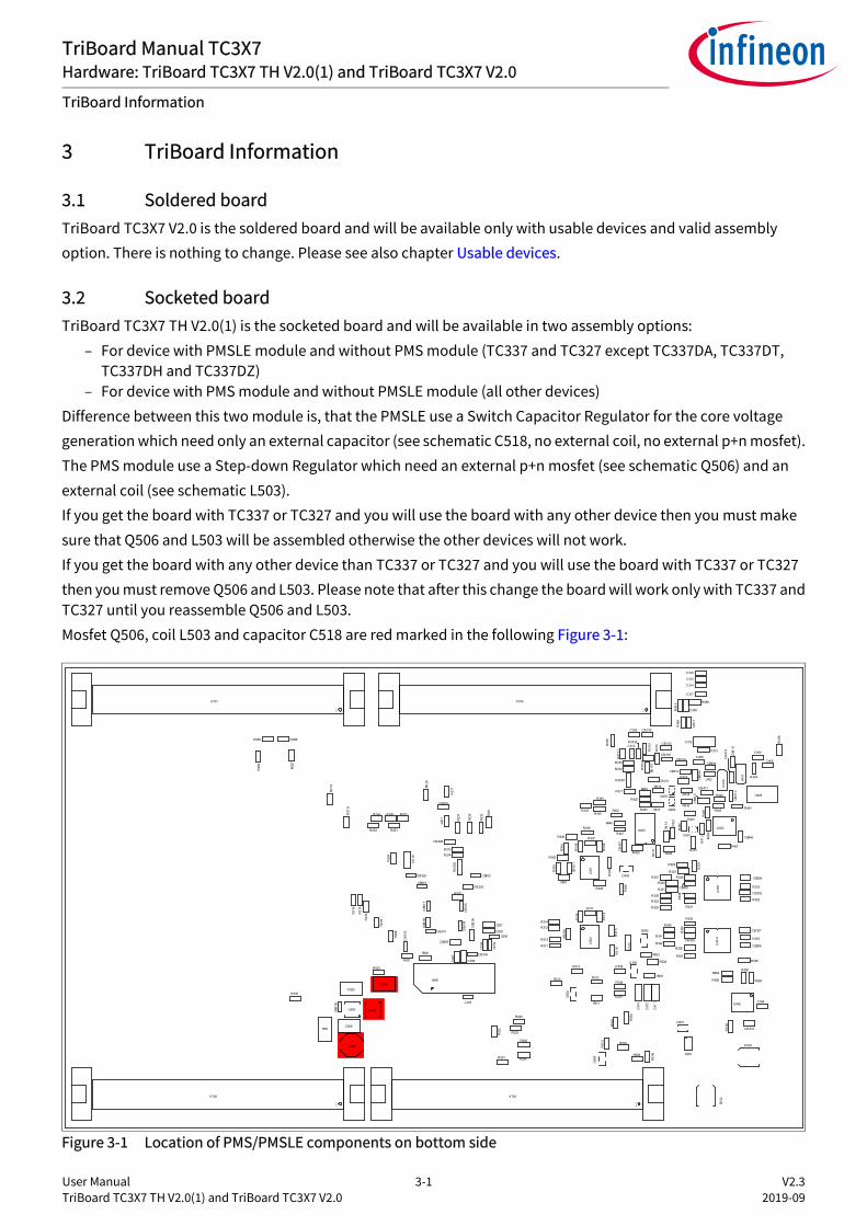
3.2 Socketed boardTriBoard TC3X7 TH V2.0(1) is the socketed board and will be available in two assembly options:
– For device with PMSLE module and without PMS module (TC337 and TC327 except TC337DA, TC337DT, TC337DH and TC337DZ)
– For device with PMS module and without PMSLE module (all other devices)Difference between this two module is, that the PMSLE use a Switch Capacitor Regulator for the core voltagegeneration which need only an external capacitor (see schematic C518, no external coil, no external p+n mosfet).The PMS module use a Step-down Regulator which need an external p+n mosfet (see schematic Q506) and anexternal coil (see schematic L503).If you get the board with TC337 or TC327 and you will use the board with any other device then you must makesure that Q506 and L503 will be assembled otherwise the other devices will not work.If you get the board with any other device than TC337 or TC327 and you will use the board with TC337 or TC327then you must remove Q506 and L503. Please note that after this change the board will work only with TC337 andTC327 until you reassemble Q506 and L503.Mosfet Q506, coil L503 and capacitor C518 are red marked in the following Figure 3-1:
Figure 3-1 Location of PMS/PMSLE components on bottom side
CB409
U503CB5
06
C506C521
C520
L503
Q506
C518
R260
R25
9
R258
R25
7
L20
1
CB209
CB208
R374R373
R325
R327
R313
R525
R438
R437
R436
R328
R326
R312
R239
R23
7
R23
5
R23
3 R23
1
R21
9
R21
8
R503
D502
C51
1
C51
2
D501
Q501
Q50
5
R5
06
R50
2
C51
0
R50
4
R505
D503
R520
CB510
R209
R21
6
R320
C408C40
7
CB203
C5
19
R353
R352
R333
R33
4
R332
U30
4U
303
R351
R35
0
R358
R331
R330
R33
8
R30
4
R30
3
CB308
CB307
CB306
CB305
CB304
CB303
R342
R302
U30
2U
301
X701 X704
X703X702
Q 503
Q50
4
Q502
R510 R512
R511
C51
5
R536
R535
CB204
R513
R53
4
R538
R317
R307
R537
CB520
CB519
CB5
18C
B51
7
CB
516
CB
515
CB
513
CB512
CB205
CB
302
CB30
1
R343
R323
R533
R52
4
R221
R220
R22
2
R322
R321
R340
R341
R311
R301
R522
R31
9
R31
8
R3
16R
315
R3
09
R3
08
R306
R30
5
CB4
04
CB406
R405
R40
6
U402
R407
CB4
03
CB
407
R409
R41
0
R415
R416R417
R418
R414
R420
C406
R41
2Q401
Q402
U403
R42
1
R422
C404
C405
CB41
0
CB411
CB4
12
R441
R442
R45
0
C401 R404
D403
C4
03C
B41
3
L402
U405
R413
R443
R445
R447
R448
R449
C304
CB310
CB2
06
R21
1
R3
60
R362
R363
R364
R365
R223
R238
R521
U306
X405
R21
4R21
5
R40
8
R20
8
R254
R253 R251
R250 R252
R314
R381
R4
31
RN
302
R523
R433
C203
C204
C205
C206
C207
C208
R245
R246
RN301
CB316
CB315
CB314
CB313
CB312
CB311
R370
R38
5R
384
R389
C308
C30
7
C305
Q403
C312
C313
C314
C315
C316
C317
C319
R31
11 R31
10R3
107
R31
06
R3105
R440R419
R372
R371
R31
0R37
8
R3
88

User Manual 3-2 V2.3 TriBoard TC3X7 TH V2.0(1) and TriBoard TC3X7 V2.0 2019-09
TriBoard Manual TC3X7Hardware: TriBoard TC3X7 TH V2.0(1) and TriBoard TC3X7 V2.0
TriBoard Information
3.2.1 Usable devices
Note: Note: Please check always the latest manual for complete list of usable/tested devices.
The board can be used with the following devices:• TC397 B-Step (except TC397XA, TC397XT and TC397QA)• TC387• TC377 (except TC377TX)• TC367• TC337 (except TC337DA, TC337DT, TC337DH and TC337DZ, planned, not yet tested)• TC327 (planned, not yet tested)• TC3E7 (planned, not yet tested)
3.2.2 Restricted usable devices• TC397 A-Step (except TC397XR and TC397XA)
– Ethernet will not work because device don’t support RGMII
• TC397 A-Step (only TC397XR and TC397XA)• TC397 B-Step (only TC397XA, TC397XT and TC397QA)• TC357• TC3A7• TC337 (only TC337DA, TC337DT, TC337DH and TC337DZ, planned, not yet tested)
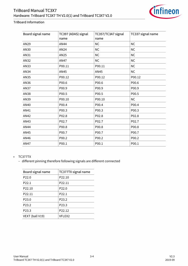
– Ethernet will not work– Select bootmode via DIP switch will not work– different pinning therefore following signals are different connected
Board signal name TC397 (ADAS) signal name
TC357/TC3A7 signal name
TC337 signal name
P00.0 P50.9 P50.9 P50.9
P00.1 P50.8 P50.8 P50.8
P00.2 P50.11 P50.11 P50.11
P00.3 P50.10 P50.10 P50.10
P00.4 P02.0 P02.0 P02.0
P00.5 P02.1 P02.1 P02.1
P00.6 P10.8 P10.8 P10.8
P00.7 P02.2 P02.2 P02.2
P00.8 P02.4 P02.4 P02.4
P00.9 P02.3 P02.3 P02.3
P00.10 P02.5 P02.5 P02.5
P00.11 P02.6 P02.6 P02.6
P00.12 P00.0 P00.0 P00.0
P01.3 P10.4 P10.4 P10.4
P01.4 P10.3 P10.3 P10.3
P01.5 P10.6 P10.6 P10.6

User Manual 3-3 V2.3 TriBoard TC3X7 TH V2.0(1) and TriBoard TC3X7 V2.0 2019-09
TriBoard Manual TC3X7Hardware: TriBoard TC3X7 TH V2.0(1) and TriBoard TC3X7 V2.0
TriBoard Information
P01.6 P10.5 P10.5 P10.5
P01.7 P10.7 P10.7 P10.7
P02.0 NC NC NC
P02.1 P50.0 P50.0 P50.0
P02.2 P50.1 P50.1 P50.1
P02.3 P50.2 P50.2 P50.2
P02.4 P50.3 P50.3 P50.3
P02.5 P50.4 P50.4 P50.4
P02.6 P50.5 P50.5 P50.5
P02.7 P50.6 P50.6 P50.6
P02.8 P50.7 P50.7 P50.7
P02.9 P10.0 P10.0 P10.0
P02.10 P10.2 P10.2 P10.2
P02.11 P10.1 P10.1 P10.1
P10.0 P51.5 P51.5 NC
P10.1 P51.4 P51.4 NC
P10.2 P51.9 P51.9 NC
P10.3 P51.7 P51.7 NC
P10.4 P51.6 P51.6 NC
P10.5 P51.8 P51.8 NC
P10.6 P51.11 P51.11 NC
P10.7 NC NC NC
P10.8 P51.10 P51.10 NC
P11.2 P11.11 P11.11 P11.11
P11.3 P11.12 P11.12 P11.12
P11.9 P51.1 P51.1 NC
P11.10 P51.0 P51.0 NC
P11.11 P51.3 P51.3 NC
P11.12 P51.2 P51.2 NC
P13.0 P11.3 P11.3 P11.3
P13.1 P11.2 P11.2 P11.2
P13.2 P11.10 P11.10 P11.10
P13.3 P11.9 P11.9 P11.9
AN24 AN38 NC NC
AN25 AN36 NC NC
AN26 AN37 NC NC
AN27 AN39 NC NC
AN28 AN46 NC NC
Board signal name TC397 (ADAS) signal name
TC357/TC3A7 signal name
TC337 signal name
User Manual 3-4 V2.3 TriBoard TC3X7 TH V2.0(1) and TriBoard TC3X7 V2.0 2019-09
TriBoard Manual TC3X7Hardware: TriBoard TC3X7 TH V2.0(1) and TriBoard TC3X7 V2.0
TriBoard Information
• TC377TX– different pinning therefore following signals are different connected
AN29 AN44 NC NC
AN30 AN24 NC NC
AN31 AN25 NC NC
AN32 AN47 NC NC
AN33 P00.11 P00.11 NC
AN34 AN45 AN45 NC
AN35 P00.12 P00.12 P00.12
AN36 P00.6 P00.6 P00.6
AN37 P00.9 P00.9 P00.9
AN38 P00.5 P00.5 P00.5
AN39 P00.10 P00.10 NC
AN40 P00.4 P00.4 P00.4
AN41 P00.3 P00.3 P00.3
AN42 P02.8 P02.8 P02.8
AN43 P02.7 P02.7 P02.7
AN44 P00.8 P00.8 P00.8
AN45 P00.7 P00.7 P00.7
AN46 P00.2 P00.2 P00.2
AN47 P00.1 P00.1 P00.1
Board signal name TC377TX signal name
P22.0 P22.10
P22.1 P22.11
P22.10 P22.0
P22.11 P22.1
P23.0 P23.2
P23.2 P23.3
P23.3 P22.12
VEXT (ball V19) VFLEX2
Board signal name TC397 (ADAS) signal name
TC357/TC3A7 signal name
TC337 signal name

User Manual 3-5 V2.3 TriBoard TC3X7 TH V2.0(1) and TriBoard TC3X7 V2.0 2019-09
TriBoard Manual TC3X7Hardware: TriBoard TC3X7 TH V2.0(1) and TriBoard TC3X7 V2.0
TriBoard Information
3.3 Power SupplyAll needed voltages are generated via Infineon’s Multi Voltage Safety Micro Processor Supply TLF35584QV and viathe microcontroller itself (+1,25V).The supply device is available as two different devices:TLF35584QVVS1 -> +5V standby voltage, +5V TriCore supply (V_UC)TLF35584QVVS2 -> +3,3V standby voltage, +3,3V TriCore supply (V_UC)Dependent of the assembled device the board works with 5V or 3,3V IO.The TLF35584QV provide the following voltages:+3,3V or +5V for standby (connected to VEVRSB)+3,3V or +5V for TriCore (connected to VEXT)+5V communcation supply (used by CAN and FlexRay™ transceivers)+5V voltage reference (connected to VDDM and VAREFx)+3,3V via LDO directly from pre regulator (used by Ethernet PHY)Applying a stable supply voltage causes the power on reset after a short period. The three LED's (V_UC, +3.3V,+1V25) indicate the status of the on board generated voltages.A manual power on reset is executed by pressing the reset button.The Board has to be connected to a +3,5V to +40V DC power supply.The power consumption is not specified yet but a supply with 12V and 500mA is recommended. The pinout forthe supply connector is shown in Figure 6-7. There can be used any standard power pack with a connector wherethe positive line is surrounded by the ground line.
3.3.1 Failsafe handlingIn case that the device don’t contains a program which disable or service the window watchdog and error pinmonitor of the TLF35584 then the TLF35584 is going to a FAILSAFE state where all supplies are switched off. Thisstate can be left via reconnect the power plug or via the ENA button (S502). In this case you must connect adebugger which is able to disable the window watchdog and error pin monitor to reprogram the microcontroller.In the default state of the board the switching to FAILSAFE state is switched off via resistor R508 (0R). If you will use/evaluate all safety features of the TLF35584 remove assembled R508. Make sure that you have aproper initialization of TLF35584 in your software.Resistor R508 is red marked in the following Figure 3-2:

User Manual 3-6 V2.3 TriBoard TC3X7 TH V2.0(1) and TriBoard TC3X7 V2.0 2019-09
TriBoard Manual TC3X7Hardware: TriBoard TC3X7 TH V2.0(1) and TriBoard TC3X7 V2.0
TriBoard Information
Figure 3-2 Resistors for TLF35584 Safety feature handling with switch on
3.4 LEDsThere are 15 LEDs on board:
– D302 up to D305 (blue) -> toogle LEDs connected to P33.4 ... P33.7– D306 up to D309 (blue) -> toogle LEDs connected to P20.11 ... P20.14– D504 RST (red) -> RESET LED indicate the reset state of the board (/ESR0)– D505 +1V25 (green) -> +1V25 power supply indication– D506 +3V3 (green) -> +3,3V power supply indication– D507 V_UC (green) -> +5V/+3,3V power supply indication– D508 SS2 (green) -> safe state signal 2 indication– D402 ACT (green) -> on board miniWiggler JDS is ACTIV– D401 RUN (blue) -> Debug RUN mode (switched by DAS Server)
3.5 ClockOn the board is a fixed crystal with 20MHz assembled. You can change this by replacing Y101 (soldered).
3.6 USB ConnectorThe USB connector is used for connection to a PC. Via the USB it is possible to power the board, using the ASCLIN0as serial connection via USB and Debugging via DAS. For the pinout of USB socket see Figure 6-8.NOTE: Before connecting the board to the PC, make sure that the actual DAS software is installed on the PC. Foractual DAS software please contact your local FAE.The software can also be found on:
DAS website
R386
C52
2
U201
X40
6
X202
R31
09
R457
R347
R34
6X502
X403
S202
R453
R349
R34
8
R376
R375
R329
R390
R25
6
R2
55
R241
R21
7
CB
502
R509
R50
8
R507
R5
01
C50
4
C5
03
C50
1
C5
08
C5
09
C507
C502
CB5
01
L50
1
L502
U501
D508
C505U502
S502
R398
CB2
01
R213
X404
R452
R354
S501
X50
1
X401
D504 D507
D506
D505
D30
9
D30
8
D30
7
D30
6
D30
5
D30
4
D30
3
D30
2
X601
X603 X602
X30
2X3
01
T30
2T
301
U305
R35
6
R35
5
R33
6
R33
5
R53
1R439
C30
2C
301
R53
2
CB
309
R397R396R395R394R393R392
R39
1
R399
R324
R3
57R
337
Y20
1
R20
7
R206
C202
C201
R202
R203
R201
R42
8
R427
R42
6
R42
5
R42
4
R344
CB402
R402
R403
CB4
08
Y401
U401
U4
04
CB4
01
R40
1
D402
L401
BU40
1
R411
C40
2 CB
405
R42
3
R429
R430
D401
CB414
CB
415
CB
416
CB
417
CB
418
CB
419
R44
4
R4
46
R45
4
R456
R45
5
R45
1
U406U407 U408
C303
D30
1
R212
R35
9
R361
R23
0
R23
2
R23
4
R23
6
R24
0
X30
3X
304
X305
X201
R205
R204
CB
202
R377 S20
1
R225
R226
X402
R244
R247
R248
R24
9
X604
Y30
1
U307
L301
CB319
CB318
C318
C309
C311
CB317
X306
C310
C3
06
C32
0
R38
3
R3108
R3104
R3102R3101R3100
R382
Q30
1 R379R380
R31
03
User Manual 3-7 V2.3 TriBoard TC3X7 TH V2.0(1) and TriBoard TC3X7 V2.0 2019-09
TriBoard Manual TC3X7Hardware: TriBoard TC3X7 TH V2.0(1) and TriBoard TC3X7 V2.0
TriBoard Information
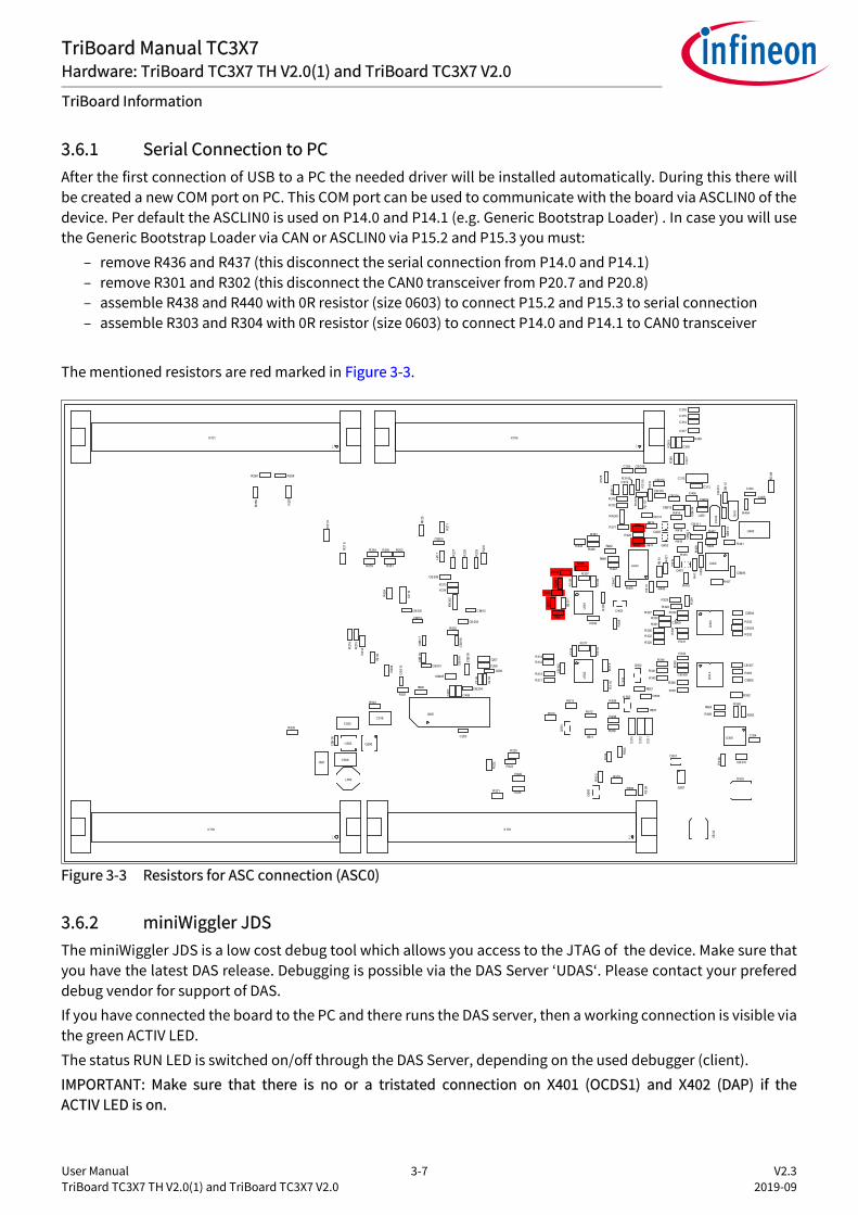
3.6.1 Serial Connection to PCAfter the first connection of USB to a PC the needed driver will be installed automatically. During this there willbe created a new COM port on PC. This COM port can be used to communicate with the board via ASCLIN0 of thedevice. Per default the ASCLIN0 is used on P14.0 and P14.1 (e.g. Generic Bootstrap Loader) . In case you will usethe Generic Bootstrap Loader via CAN or ASCLIN0 via P15.2 and P15.3 you must:
– remove R436 and R437 (this disconnect the serial connection from P14.0 and P14.1)– remove R301 and R302 (this disconnect the CAN0 transceiver from P20.7 and P20.8)– assemble R438 and R440 with 0R resistor (size 0603) to connect P15.2 and P15.3 to serial connection– assemble R303 and R304 with 0R resistor (size 0603) to connect P14.0 and P14.1 to CAN0 transceiver
The mentioned resistors are red marked in Figure 3-3.
Figure 3-3 Resistors for ASC connection (ASC0)
3.6.2 miniWiggler JDSThe miniWiggler JDS is a low cost debug tool which allows you access to the JTAG of the device. Make sure thatyou have the latest DAS release. Debugging is possible via the DAS Server ‘UDAS‘. Please contact your prefereddebug vendor for support of DAS.If you have connected the board to the PC and there runs the DAS server, then a working connection is visible viathe green ACTIV LED.The status RUN LED is switched on/off through the DAS Server, depending on the used debugger (client).IMPORTANT: Make sure that there is no or a tristated connection on X401 (OCDS1) and X402 (DAP) if theACTIV LED is on.
CB409
U503CB5
06
C506C521
C520
L503
Q506
C518
R260
R25
9
R258
R25
7
L20
1
CB209
CB208
R374R373
R325
R327
R313
R525
R438
R437
R436
R328
R326
R312
R239
R23
7
R23
5
R23
3 R23
1
R21
9
R21
8
R503
D502
C51
1
C51
2
D501
Q501
Q50
5
R5
06
R50
2
C51
0
R50
4
R505
D503
R520
CB510
R209
R21
6
R320
C408C40
7
CB203
C5
19
R353
R352
R333
R33
4
R332
U30
4U
303
R351
R35
0
R358
R331
R330
R33
8
R30
4
R30
3
CB308
CB307
CB306
CB305
CB304
CB303
R342
R302
U30
2U
301
X701 X704
X703X702
Q 503
Q50
4
Q502
R510 R512
R511
C51
5
R536
R535
CB204
R513
R53
4
R538
R317
R307
R537
CB520
CB519
CB5
18C
B51
7
CB
516
CB
515
CB
513
CB512
CB205
CB
302
CB30
1
R343
R323
R533
R52
4
R221
R220
R22
2
R322
R321
R340
R341
R311
R301
R522
R31
9
R31
8
R3
16R
315
R3
09
R3
08
R306
R30
5
CB4
04
CB406
R405
R40
6
U402
R407
CB4
03
CB
407
R409
R41
0
R415
R416R417
R418
R414
R420
C406
R41
2Q401
Q402
U403
R42
1
R422
C404
C405
CB41
0
CB411
CB4
12
R441
R442
R45
0
C401 R404
D403
C4
03C
B41
3
L402
U405
R413
R443
R445
R447
R448
R449
C304
CB310
CB2
06
R21
1
R3
60
R362
R363
R364
R365
R223
R238
R521
U306
X405
R21
4R21
5
R40
8
R20
8
R254
R253 R251
R250 R252
R314
R381
R4
31
RN
302
R523
R433
C203
C204
C205
C206
C207
C208
R245
R246
RN301
CB316
CB315
CB314
CB313
CB312
CB311
R370
R38
5R
384
R389
C308
C30
7
C305
Q403
C312
C313
C314
C315
C316
C317
C319
R31
11 R31
10R3
107
R31
06
R3105
R440R419
R372
R371
R31
0R37
8
R3
88

User Manual 3-8 V2.3 TriBoard TC3X7 TH V2.0(1) and TriBoard TC3X7 V2.0 2019-09
TriBoard Manual TC3X7Hardware: TriBoard TC3X7 TH V2.0(1) and TriBoard TC3X7 V2.0
TriBoard Information
Per default the miniWiggler is connected to the DAP. It is possible to change the connection to DAPE (DAP ofemulation device if available). If resistors R214, R215 and R216 assembled (default) then the standard DAP isconnected to miniWiggler otherwise if R217, R218 and R219 are assembled the the DAPE of emulation device isconnected to miniWiggler. Please note that there should be connected only standard DAP or DAPE. If all thisresistors are not assembled then the miniWiggler can’t be used. In this case only the DAP connectors X402 andX403 can be used. See Figure 3-8 and Figure 3-9.
3.7 FlexRay™ (E-RAY)The board has 2 IDC10 plugs for FlexRay™ Communication (channel A and B) with up to 10 Mbit/s. For the pinoutof the plugs see Figure 6-9. You can use a IDC female connector with crimpconnector, flat cable and SUB-D 9 plugwith crimpconnector to have a 1:1 adapter to SUB-D 9.The transceiver are connected to the TriCore device via zero ohm resistors (R325 up to R329 and R340 up to R344)which must be removed to use the ports outside.ERAY-A can be connected to P14.8, P14.9 and P14.10 (default, usable with ERAY0 and ERAY1) and to P02.0, P02.1and P02.4 (only usable with ERAY0). Transceiver for channel A can be enabled/disabled via P32.3 (default) or viaP10.2. The error state of transceiver channel A can be read out via P32.2 (default) or via P10.1.ERAY-B is connected to P14.5, P14.6 and P14.7 (default, usable with ERAY0 and ERAY1). Transceiver for channel Acan be enabled/disabled via P20.10 (default). The error state of transceiver channel A can be read out via P20.9(default).For more information look in the user manual for TC3X7.
Note: TC327 don’t support FlexRay™.
3.8 Serial Eeprom
Note: TC337 don’t have I2C module. Access to the eeprom only with simulation of I2C protocol via bit banging possible.
The I2C via P15.4 and P15.5 of the TC3X7 is connected to a serial EEPROM with a size of 2KBit (2 x 128 x 8). The slaveaddress of this EEPROM is 0x50. The upper half of the array (80h-FFh) is permanently write-protected. Writeoperations to this address range are inhibited. Read operations are not affected. This upper half contains a pre-programmed EUI-48™ node address which can be used as MAC ID for Ethernet. The other 128 bytes are writableby customer.To disconnect (disable) the EEPROM remove resistor R348 and R349.
3.9 MultiCANOn the board are two CAN transceiver connected to the CAN0 and CAN1 of TC3X7. The transceivers are connectedto two IDC10 plug. For the pinout of IDC10 plug see Figure 6-10. You can use a IDC female connector withcrimpconnector, flat cable and SUB-D 9 plug with crimpconnector to have a 1:1 adapter to SUB-D 9.The transceiver are connected to the TriCore device via zero ohm resistors (R301 up to R304 and R311 up to R314)which must be removed to use the ports outside.CAN0 can be used via P20.7 and P20.8 (node 0, default) or P14.0 and P14.1 (node 1). CAN1 can be used via P23.0and P23.1 (node 0, default) or P00.0 and P00.1 (node 0).
Note: CAN1 on TC337 is only usable via P00.0 and P00.1 (P23.0 don’t exist).

User Manual 3-9 V2.3 TriBoard TC3X7 TH V2.0(1) and TriBoard TC3X7 V2.0 2019-09
TriBoard Manual TC3X7Hardware: TriBoard TC3X7 TH V2.0(1) and TriBoard TC3X7 V2.0
TriBoard Information
3.10 LINOn the board is one LIN transceiver connected to the ASCLIN1 on TC3X7 (P15.0 and P15.1). The transceiver areconnected to one IDC10 plug. For the pinout of IDC10 plug see Figure 6-11. You can use a IDC female connectorwith crimpconnector, flat cable and SUB-D 9 plug with crimpconnector to have a 1:1 adapter to SUB-D 9.To disconnect the LIN remove resistor R364 and R365. The LIN can be used in master and in slave mode. For the master mode there is per default a pull-up of 1K (R360)and a capacitor of 1nF (C304) on the BUS assembled. For using the LIN in slave mode the pull-up resistor R360must be removed and maybe the capacitor changed to a smaller value (e.g. 220pF).The mentioned resistor and capacitor are red marked in Figure 3-4
Figure 3-4 Components for LIN Master Mode
3.11 EthernetThe TriBoard provide a RJ45 connector (X306) for twisted pair ethernet connections.The TriBoard use a RealtekIntegrated 10/100/1000M Ethernet Precision Transceiver RTL8211FI-CG as physical interface device. For moreinformation about the ethernet modul see TC3X9 User’s Manual, about the PHY see the RTL8211F datasheet. Forthe pinout of RJ45 see Figure 6-13.The PHY is connected to the TriCore device via resistors and resistor arrays (R370 up to R374 and RN301 up toRN302).For the connection between TriCore and PHY is used RGMII.
Note: Please note that the used signals for RGMII (P11.0 up to P11.12) are not connected to any connector.
Note: TC327 and TC337 don’t support ethernet.
CB409
U503CB5
06
C506C521
C520
L503
Q506
C518
R260
R25
9
R258
R25
7
L20
1
CB209
CB208
R374R373
R325
R327
R313
R525
R438
R437
R436
R328
R326
R312
R239
R23
7
R23
5
R23
3 R23
1
R21
9
R21
8
R503
D502
C51
1
C51
2
D501
Q501
Q50
5
R5
06
R50
2
C51
0
R50
4
R505
D503
R520
CB510
R209
R21
6
R320
C408C40
7
CB203
C5
19
R353
R352
R333
R33
4
R332
U30
4U
303
R351
R35
0
R358
R331
R330
R33
8
R30
4
R30
3
CB308
CB307
CB306
CB305
CB304
CB303
R342
R302
U30
2U
301
X701 X704
X703X702
Q 503
Q50
4
Q502
R510 R512
R511
C51
5
R536
R535
CB204
R513
R53
4
R538
R317
R307
R537
CB520
CB519
CB5
18C
B51
7
CB
516
CB
515
CB
513
CB512
CB205
CB
302
CB30
1
R343
R323
R533
R52
4
R221
R220
R22
2
R322
R321
R340
R341
R311
R301
R522
R31
9
R31
8
R3
16R
315
R3
09
R3
08
R306
R30
5
CB4
04
CB406
R405
R40
6
U402
R407
CB4
03
CB
407
R409
R41
0
R415
R416R417
R418
R414
R420
C406
R41
2Q401
Q402
U403
R42
1
R422
C404
C405
CB41
0
CB411
CB4
12
R441
R442
R45
0
C401 R404
D403
C4
03C
B41
3
L402
U405
R413
R443
R445
R447
R448
R449
C304
CB310
CB2
06
R21
1
R3
60
R362
R363
R364
R365
R223
R238
R521
U306
X405
R21
4R21
5
R40
8
R20
8
R254
R253 R251
R250 R252
R314
R381
R4
31
RN
302
R523
R433
C203
C204
C205
C206
C207
C208
R245
R246
RN301
CB316
CB315
CB314
CB313
CB312
CB311
R370
R38
5R
384
R389
C308
C30
7
C305
Q403
C312
C313
C314
C315
C316
C317
C319
R31
11 R31
10R3
107
R31
06
R3105
R440R419
R372
R371
R31
0R37
8
R3
88

User Manual 3-10 V2.3 TriBoard TC3X7 TH V2.0(1) and TriBoard TC3X7 V2.0 2019-09
TriBoard Manual TC3X7Hardware: TriBoard TC3X7 TH V2.0(1) and TriBoard TC3X7 V2.0
TriBoard Information
3.12 HSCT (optional)The TriBoard provide a footprint of IEEE 1394 socket (X201 and X202) for connection to other TC3XX via HSCT.
Note: Don’t use X201 and X202 for connection to any IEEE 1394 device, this can destroy the board and/or the connected device.
X201 is connected to HSCT0 and X202 to HSCT1 of the used device (if used microcontroller support second HSCT).For connect two TriBoards you need to assemble this socket (Lumberg 2415 01) on each board and connect theboards with a standard 6 pin IEEE 1394 cable. For the pinout of socket see Figure 6-12.
Note: TC327 and TC337 don’t support HSCT.
Note: HSCT1 only usable with TC397.
3.12.1 High speed with HSCTFor use the HSCT connection between two board you need to remove 9 resistors to have a very short connectionbetween device and connector. On the TC3X7 Triboard this 9 resistors are R250, R251, R252, R253, R254, R257,R258, R259 and R260 (red marked in Figure 3-5). This resistors needs to be removed.mportant: When the resistors are removed then the port signals P20.0, P21.2, P21.3, P21.4, P21.5, P21.0, P21.1,P22.2 and P22.3 are no longer available on the 80 pin samtec connectors.

User Manual 3-11 V2.3 TriBoard TC3X7 TH V2.0(1) and TriBoard TC3X7 V2.0 2019-09
TriBoard Manual TC3X7Hardware: TriBoard TC3X7 TH V2.0(1) and TriBoard TC3X7 V2.0
TriBoard Information
Figure 3-5 Resistors for high speed HSCT
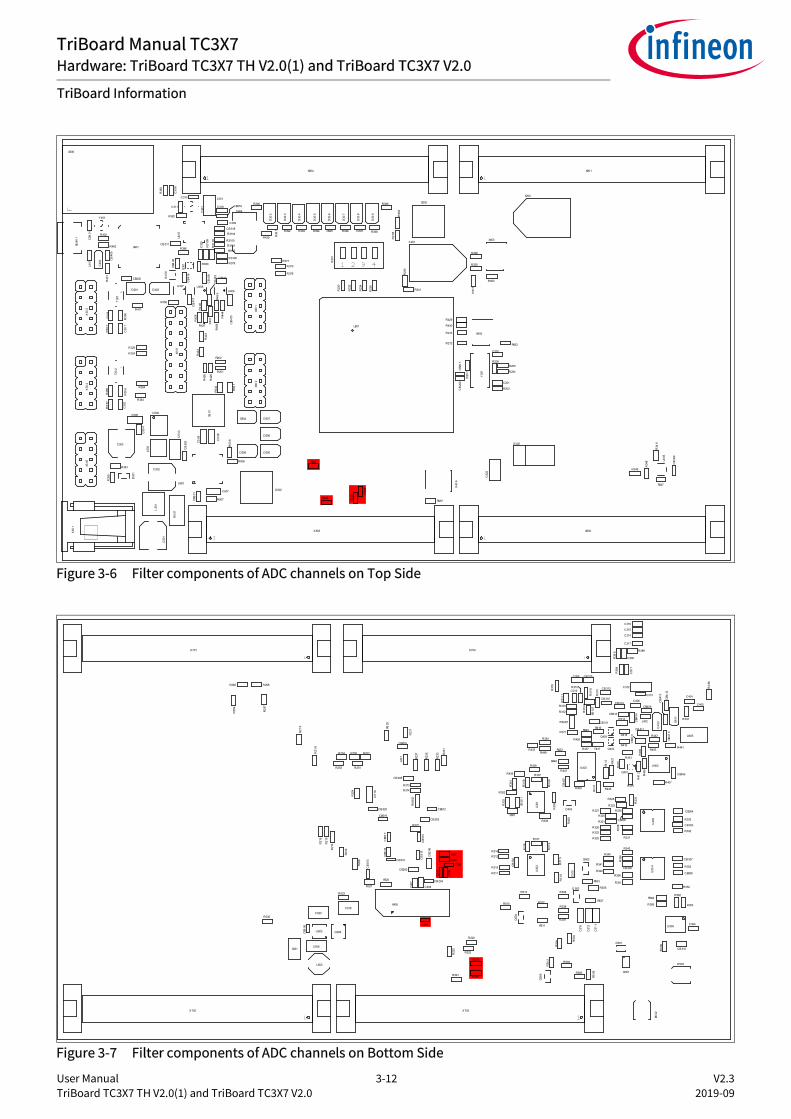
3.13 ADCOn this boards are 6 ADC channels prepared with a low pass filter. On pin AN7, AN20, AN21, AN31, AN44 and AN45is assembled a capacitor of 47nF and a serial resistor of 4,7K. The filter components are red marked in thefollowing figures (Figure 3-6 and Figure 3-7).
CB409
U503CB5
06
C506C521
C520
L503
Q506
C518
R260
R25
9
R258
R25
7
L20
1
CB209
CB208
R374R373
R325
R327
R313R5
25
R438
R437
R436
R328
R326
R312
R239
R23
7
R23
5
R23
3 R23
1
R21
9
R21
8
R503
D502
C51
1
C51
2
D501
Q501
Q50
5
R5
06
R50
2
C51
0
R50
4
R505
D503
R520
CB510
R209
R21
6
R320
C408C40
7
CB203
C5
19
R353
R352
R333
R33
4
R332
U30
4U
303
R351
R35
0
R358
R331
R330
R33
8
R30
4
R30
3
CB308
CB307
CB306
CB305
CB304
CB303
R342
R302
U30
2U
301
X701 X704
X703X702
Q 503
Q50
4
Q502
R510 R512
R511
C51
5
R536
R535
CB204
R513
R53
4
R538
R317
R307
R537
CB520
CB519
CB5
18C
B51
7
CB
516
CB
515
CB
513
CB512
CB205
CB
302
CB30
1
R343
R323
R533
R52
4
R221
R220
R22
2
R322
R321
R340
R341
R311
R301
R522
R31
9
R31
8
R3
16R
315
R3
09
R3
08
R306
R30
5
CB4
04
CB406
R405
R40
6
U402
R407
CB4
03
CB
407
R409
R41
0
R415
R416R417
R418
R414
R420
C406
R41
2Q401
Q402
U403
R42
1
R422
C404
C405
CB41
0
CB411
CB4
12
R441
R442
R45
0
C401 R404
D403
C4
03C
B41
3
L402
U405
R413
R443
R445
R447
R448
R449
C304
CB310
CB2
06
R21
1
R3
60
R362
R363
R364
R365
R223
R238
R521
U306
X405
R21
4R21
5
R40
8
R20
8
R254
R253 R251
R250 R252
R314
R381
R4
31
RN
302
R523
R433
C203C2
04
C205
C206
C207
C208
R245
R246
RN301
CB316
CB315
CB314
CB313
CB312
CB311
R370
R38
5R
384
R389
C308
C30
7
C305
Q403
C312
C313
C314
C315
C316
C317
C319
R31
11 R31
10R3
107
R31
06
R3105
R440R419
R372
R371
R31
0R37
8
R3
88
User Manual 3-12 V2.3 TriBoard TC3X7 TH V2.0(1) and TriBoard TC3X7 V2.0 2019-09
TriBoard Manual TC3X7Hardware: TriBoard TC3X7 TH V2.0(1) and TriBoard TC3X7 V2.0
TriBoard Information
Figure 3-6 Filter components of ADC channels on Top Side
Figure 3-7 Filter components of ADC channels on Bottom Side
R386
C52
2
U201
X40
6
X202
R31
09
R457
R347
R34
6X502
X403
S202
R453
R349
R34
8
R376
R375
R329
R390
R25
6
R2
55
R241
R21
7
CB
502
R509
R50
8
R507
R5
01
C50
4
C5
03
C50
1
C5
08
C5
09
C507
C502
CB5
01
L50
1
L502
U501
D508
C505U502
S502
R398
CB2
01
R213
X404
R452
R354
S501
X50
1
X401
D504 D507
D506
D505
D30
9
D30
8
D30
7
D30
6
D30
5
D30
4
D30
3
D30
2
X601
X603 X602
X30
2X3
01
T30
2T
301
U305
R35
6
R35
5
R33
6
R33
5
R53
1R439
C30
2C
301
R53
2
CB
309
R397R396R395R394R393R392
R39
1
R399
R324
R3
57R
337
Y20
1
R20
7
R206
C202
C201
R202
R203
R201
R42
8
R427
R42
6
R42
5
R42
4
R344
CB402
R402
R403
CB4
08
Y401
U401
U4
04
CB4
01
R40
1
D402
L401
BU40
1
R411
C40
2 CB
405
R42
3
R429
R430
D401
CB414
CB
415
CB
416
CB
417
CB
418
CB
419
R44
4
R4
46
R45
4
R456
R45
5
R45
1
U406U407 U408
C303
D30
1
R212
R35
9
R361
R23
0
R23
2
R23
4
R23
6
R24
0
X30
3X
304
X305
X201
R205
R204
CB
202
R377 S20
1
R225
R226
X402
R244
R247
R248
R24
9
X604
Y30
1
U307
L301
CB319
CB318
C318
C309
C311
CB317
X306
C310
C3
06
C32
0
R38
3
R3108
R3104
R3102R3101R3100
R382
Q30
1 R379R380
R31
03
CB409
U503CB5
06
C506C521
C520
L503
Q506
C518
R260
R25
9
R258
R25
7
L20
1
CB209
CB208
R374R373
R325
R327
R313
R525
R438
R437
R436
R328
R326
R312
R239
R23
7
R23
5
R23
3 R23
1
R21
9
R21
8
R503
D502
C51
1
C51
2
D501
Q501
Q50
5
R5
06
R50
2
C51
0
R50
4
R505
D503
R520
CB510
R209
R21
6
R320
C408C40
7
CB203
C5
19
R353
R352
R333
R33
4
R332
U30
4U
303
R351
R35
0
R358
R331
R330
R33
8
R30
4
R30
3
CB308
CB307
CB306
CB305
CB304
CB303
R342
R302
U30
2U
301
X701 X704
X703X702
Q 503
Q50
4
Q502
R510 R512
R511
C51
5
R536
R535
CB204
R513
R53
4
R538
R317
R307
R537
CB520
CB519
CB5
18C
B51
7
CB
516
CB
515
CB
513
CB512
CB205
CB
302
CB30
1
R343
R323
R533
R52
4
R221
R220
R22
2
R322
R321
R340
R341
R311
R301
R522
R31
9
R31
8
R3
16R
315
R3
09
R3
08
R306
R30
5
CB4
04
CB406
R405
R40
6
U402
R407
CB4
03
CB
407
R409
R41
0
R415
R416R417
R418
R414
R420
C406
R41
2Q401
Q402
U403
R42
1
R422
C404
C405
CB41
0
CB411
CB4
12
R441
R442
R45
0
C401 R404
D403
C4
03C
B41
3
L402
U405
R413
R443
R445
R447
R448
R449
C304
CB310
CB2
06
R21
1
R3
60
R362
R363
R364
R365
R223
R238
R521
U306
X405
R21
4R21
5
R40
8
R20
8
R254
R253 R251
R250 R252
R314
R381
R4
31
RN
302
R523
R433
C203
C204
C205
C206
C207
C208
R245
R246
RN301
CB316
CB315
CB314
CB313
CB312
CB311
R370
R38
5R
384
R389
C308
C30
7
C305
Q403
C312
C313
C314
C315
C316
C317
C319
R31
11 R31
10R3
107
R31
06
R3105
R440R419
R372
R371
R31
0R37
8
R3
88

User Manual 3-13 V2.3 TriBoard TC3X7 TH V2.0(1) and TriBoard TC3X7 V2.0 2019-09
TriBoard Manual TC3X7Hardware: TriBoard TC3X7 TH V2.0(1) and TriBoard TC3X7 V2.0
TriBoard Information
3.14 Other peripheralsFor all other peripherals there are no special plugs on the board. The peripheral signals are available on thedifferent connectors. See “Connector Pin Assignment” on Page 6-1.
3.15 Toggle LED’sThe status LED’s are low active and can be controlled by Software.Port 20 pin 11 up to pin 14 are connected to single LED’s (D306... D309) and powered by the normalmicrocontroller voltage.Port 33 pin 4 up to pin 7 are connected to single LED’s (D302... D305) and powered by the standby voltage. Thismeans that this LED’s can be are activ also when the board is in standby mode and only the standby voltageavailable (port 33 is powered by VEVRSB pin which is connected to standby supply of TLF35584). In this case theport pins are controlled by the standby controller if available.
3.16 ButtonsOn the board are three buttons.The reset button (S501) will apply a warm power on reset to the device.The ENA button (S502) will be used to enable/wakeup the TLF35584.The P33.11 button (S202) can be used by software as input. Also can this button used by the standby controllerto react on an event when only standby supply is available (e.g. wakeup the TLF35584 via P33.10).
3.17 Debug System
3.17.1 OCDS1The OCDS1 signals are connected to the IDC16 plug (X401). They work with the port supply of Microcontroller (+5Vdefault or +3,3V). For pinout of the connector see Figure 6-14. You can connect any debugger to this connector. The signals /BRKIN and /BRKOUT are not connected per default. If you need this signals in the connector thenassemble R424 and R425 or R426 with a 0R resistor.If you connect a debug hardware make sure that the miniWiggler JDS (see “miniWiggler JDS” on Page 3-7) is notactiv (ACTIV LED is off) and on the DAP connector (X402) is no hardware connected or the hardware is tristated. If the ACTIV LED is on, then stop the active DAS Server ’UDAS’ and/or remove the USB connection to the PC.In case that R217, R218 and R219 are assembled instead of R214, R215 and R216 then the connector can be usedonly for DAP connection to DAPE. If R214 up to R219 not assembled then the connector is not usable.
3.17.2 DAPThe board comes with a DAP connector (X402). For pinout of this connector see Figure 6-15. You can connect aDAP hardware here. If you use this connector make sure that the miniWiggler JDS is not activ (ACTIV LED is off)and a connected OCDS1 hardware is disconnected or tristated.
3.17.3 DAPE (only Emulation Device)The board comes also with another DAP connector (X403) which is connected to DAPE in case that an emulationdevice is used. For pinout of this connector see Figure 6-15. You can connect a DAP hardware here. If you use thisconnector make sure that the miniWiggler JDS is not activ (ACTIV LED is off) and a connected OCDS1 hardware isdisconnected or tristated in case that R217, R218 and R219 are assembled.
User Manual 3-14 V2.3 TriBoard TC3X7 TH V2.0(1) and TriBoard TC3X7 V2.0 2019-09
TriBoard Manual TC3X7Hardware: TriBoard TC3X7 TH V2.0(1) and TriBoard TC3X7 V2.0
TriBoard Information
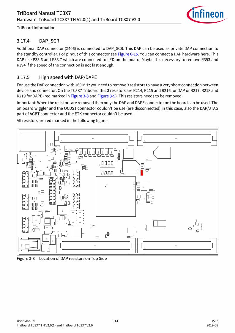
3.17.4 DAP_SCRAdditional DAP connector (X406) is connected to DAP_SCR. This DAP can be used as private DAP connection tothe standby controller. For pinout of this connector see Figure 6-15. You can connect a DAP hardware here. ThisDAP use P33.6 and P33.7 which are connected to LED on the board. Maybe it is necessary to remove R393 andR394 if the speed of the connection is not fast enough.
3.17.5 High speed with DAP/DAPEFor use the DAP connection with 160 MHz you need to remove 3 resistors to have a very short connection betweendevice and connector. On the TC3X7 Triboard this 3 resistors are R214, R215 and R216 for DAP or R217, R218 andR219 for DAPE (red marked in Figure 3-8 and Figure 3-9). This resistors needs to be removed. Important: When the resistors are removed then only the DAP and DAPE connector on the board can be used. Theon board wiggler and the OCDS1 connector couldn’t be use (are disconnected) in this case, also the DAP/JTAGpart of AGBT connector and the ETK connector couldn’t be used.All resistors are red marked in the following figures:
Figure 3-8 Location of DAP resistors on Top Side
R386
C52
2
U201
X40
6
X202
R31
09
R457
R347
R34
6X502
X403
S202
R453
R349
R34
8
R376
R375
R329
R390
R25
6
R2
55
R241
R21
7
CB
502
R509
R50
8
R507
R5
01
C50
4
C5
03
C50
1
C5
08
C5
09
C507
C502
CB5
01
L50
1
L502
U501
D508
C505U502
S502
R398
CB2
01
R213
X404
R452
R354
S501
X50
1
X401
D504 D507
D506
D505
D30
9
D30
8
D30
7
D30
6
D30
5
D30
4
D30
3
D30
2
X601
X603 X602
X30
2X3
01
T30
2T
301
U305
R35
6
R35
5
R33
6
R33
5
R53
1
R439
C30
2C
301
R53
2
CB
309
R397R396R395R394R393R392
R39
1
R399
R324
R3
57R
337
Y20
1
R20
7
R206
C202
C201
R202
R203
R201
R42
8
R427
R42
6
R42
5
R42
4
R344
CB402
R402
R403
CB4
08
Y401
U401
U4
04
CB4
01
R40
1
D402
L401
BU40
1
R411
C40
2 CB
405
R42
3
R429
R430
D401
CB414
CB
415
CB
416
CB
417
CB
418
CB
419
R44
4
R4
46
R45
4
R456
R45
5
R45
1
U406U407 U408
C303
D30
1
R212
R35
9
R361
R23
0
R23
2
R23
4
R23
6
R24
0
X30
3X
304
X305
X201
R205
R204
CB
202
R377 S20
1
R225
R226
X402
R244
R247
R248
R24
9
X604
Y30
1
U307
L301
CB319
CB318
C318
C309
C311
CB317
X306
C310
C3
06
C32
0
R38
3
R3108
R3104
R3102R3101R3100
R382
Q30
1 R379R380
R31
03

User Manual 3-15 V2.3 TriBoard TC3X7 TH V2.0(1) and TriBoard TC3X7 V2.0 2019-09
TriBoard Manual TC3X7Hardware: TriBoard TC3X7 TH V2.0(1) and TriBoard TC3X7 V2.0
TriBoard Information
Figure 3-9 Location of DAP resistors on Bottom Side
3.17.6 AGBT (optional)The TriBoard provide a 22 pin high speed samtec connector (X405) for highest speed connection via AGBT. Thisconnector should be assembled by your self if needed.The AGBT interface is only available on emulation devices.For the pinout of connector see Figure 6-18.The needed Samtec connector is: ASP-137969-01 (serie ERM8, Nexus HS22).
Note: The robustness of AGBT communication depends on the PCB high-speed design quality and the physical connection of a microcontroller on the board. It is highly recommended to use boards with properly soldered microcontrollers for the highest reliability of the AGBT in the full operating range.
3.17.7 ETK connector (optional)The TriBoard provide a 10 pin samtec connector (X404) for connecting to an ETK. This connector should beassembled by your self if needed.For the pinout of connector see Figure 6-16.The needed Samtec connector is: TFM-105-02-A.
3.17.8 EmW Power (optional)The TriBoard provide the 4 pin power connector (X502) for the Ethernet miniWiggler (EmW). This connectorshould be assembled by your self if needed.For the pinout of connector see Figure 6-17.
CB409
U503CB5
06
C506C521
C520
L503
Q506
C518
R260
R25
9
R258
R25
7
L20
1
CB209
CB208
R374R373
R325
R327
R313R5
25
R438
R437
R436
R328
R326
R312
R239
R23
7
R23
5
R23
3 R23
1
R21
9
R21
8
R503
D502
C51
1
C51
2
D501
Q501
Q50
5
R5
06
R50
2
C51
0
R50
4
R505
D503
R520
CB510
R209
R21
6
R320
C408C40
7
CB203
C5
19
R353
R352
R333
R33
4
R332
U30
4U
303
R351
R35
0
R358
R331
R330
R33
8
R30
4
R30
3
CB308
CB307
CB306
CB305
CB304
CB303
R342
R302
U30
2U
301
X701 X704
X703X702
Q 503
Q50
4
Q502
R510 R512
R511
C51
5
R536
R535
CB204
R513
R53
4
R538
R317
R307
R537
CB520
CB519
CB5
18C
B51
7
CB
516
CB
515
CB
513
CB512
CB205
CB
302
CB30
1
R343
R323
R533
R52
4
R221
R220R
222
R322
R321
R340
R341
R311
R301
R522
R31
9
R31
8
R3
16R
315
R3
09
R3
08
R306
R30
5
CB4
04
CB406
R405
R40
6
U402
R407
CB4
03
CB
407
R409
R41
0
R415
R416R417
R418
R414
R420
C406
R41
2Q401
Q402
U403
R42
1
R422
C404
C405
CB41
0
CB411
CB4
12
R441
R442
R45
0
C401 R404
D403
C4
03C
B41
3
L402
U405
R413
R443
R445
R447
R448
R449
C304
CB310
CB2
06
R21
1
R3
60
R362
R363
R364
R365
R223
R238
R521
U306
X405
R21
4R21
5
R40
8
R20
8
R254
R253 R251
R250 R252
R314
R381
R4
31
RN
302
R523
R433
C203C2
04
C205
C206
C207
C208
R245
R246
RN301
CB316
CB315
CB314
CB313
CB312
CB311
R370
R38
5R
384
R389
C308
C30
7
C305
Q403
C312
C313
C314
C315
C316
C317
C319
R31
11 R31
10R3
107
R31
06
R3105
R440R419
R372
R371
R31
0R37
8
R3
88

User Manual 3-16 V2.3 TriBoard TC3X7 TH V2.0(1) and TriBoard TC3X7 V2.0 2019-09
TriBoard Manual TC3X7Hardware: TriBoard TC3X7 TH V2.0(1) and TriBoard TC3X7 V2.0
TriBoard Information
The needed Samtec connector is the JST B4B-PH-K.The connector provide the input voltage to the Ethernet miniWiggler and an enable/wakeup signal connected toTLF35584 and a standby voltage of +1,25V connected to VDDSB of device. In case the EmW is used you mustremove R522. If R522 is removed then you must make sure that the EmW is always connected. Otherwise withassembled R522 (default) you should not connect the pin 4 of connector.The mentioned resistor is red marked in Figure 3-10
Figure 3-10 Resistor for VDDSB
CB409
U503CB5
06
C506C521
C520
L503
Q506
C518
R260
R25
9
R258
R25
7
L20
1
CB209
CB208
R374R373
R325
R327
R313
R525
R438
R437
R436
R328
R326
R312
R239
R23
7
R23
5
R23
3 R23
1
R21
9
R21
8
R503
D502
C51
1
C51
2D501
Q501
Q50
5
R5
06
R50
2
C51
0
R50
4
R505
D503
R520
CB510
R209
R21
6
R320
C408C40
7
CB203
C5
19
R353
R352
R333
R33
4
R332
U30
4U
303
R351
R35
0
R358
R331
R330
R33
8
R30
4
R30
3
CB308
CB307
CB306
CB305
CB304
CB303
R342
R302
U30
2U
301
X701 X704
X703X702
Q 503
Q50
4
Q502
R510 R512
R511C
515
R536
R535
CB204
R513
R53
4
R538
R317
R307
R537
CB520
CB519
CB5
18C
B51
7
CB
516
CB
515
CB
513
CB512
CB205C
B30
2
CB30
1
R343
R323
R533
R52
4
R221
R220
R22
2
R322
R321
R340
R341
R311
R301
R522
R31
9
R31
8
R3
16R
315
R3
09
R3
08
R306
R30
5
CB4
04
CB406
R405
R40
6
U402
R407
CB4
03
CB
407
R409
R41
0
R415
R416R417
R418
R414
R420
C406
R41
2Q401
Q402
U403
R42
1
R422
C404
C405
CB41
0
CB411
CB4
12
R441
R442
R45
0
C401 R404
D403
C4
03C
B41
3
L402
U405
R413
R443
R445
R447
R448
R449
C304
CB310
CB2
06
R21
1
R3
60
R362
R363
R364
R365
R223
R238
R521
U306
X405
R21
4R21
5
R40
8
R20
8
R254
R253 R251
R250 R252
R314
R381
R4
31
RN
302
R523
R433
C203
C204
C205
C206
C207
C208
R245
R246
RN301
CB316
CB315
CB314
CB313
CB312
CB311
R370
R38
5R
384
R389
C308
C30
7
C305
Q403
C312
C313
C314
C315
C316
C317
C319
R31
11 R31
10R3
107
R31
06
R3105
R440R419
R372
R371
R31
0R37
8
R3
88

User Manual 4-1 V2.3 TriBoard TC3X7 TH V2.0(1) and TriBoard TC3X7 V2.0 2019-09
TriBoard Manual TC3X7Hardware: TriBoard TC3X7 TH V2.0(1) and TriBoard TC3X7 V2.0
TriBoard Configuration
4 TriBoard Configuration
4.1 HW Boot Configuration
Figure 4-1 HW Configuration DIP-Switches
The picture above shows the definition of the boot HW configuration switch. The meaning of the switches will bedescribed in the following table (Table 4-1).
Note: The ON position of the switch is equal to a logical LOW at the dedicated pin.
4.1.1 Default Pad StateP14.4 / HWCFG6 is used to select the Default Pad State. Dipswitch 1 used to select this.In case that dispswitch1 is set to ON then all I/O pins are in tristate otherwise the internal pull-up devices areenabled on the I/O pins. Please note that after change Dipswitch 1 you must make a power cycle (switch off ->switch on) to use the new configuration.In case that TriState is selected (Dipswitch 1 is set to ON) then the I/O pins are floating. If you need a specific levelon different pins during startup (e.g. driver pins) then you must add the needed pull device (up or down). Somepins (especially the HWCFG pins) haven always the needed external pull-up and/or pull-down resistor assembledon the board.
4.1.2 Bootmode
Table 4-1 User Startup Modes 1)2)3)
1) The shadowed line indicates the default setting.2) ’x’ represents the don’t care state.3) 2 to 4 are the Dip Switch numbers.
HWCFG[5...3] Type of Boot 2 3 4
XX1 Start-up mode is selected by Boot Mode Index X X OFF
110 Internal Start from Flash OFF OFF ON
100 Alternate Boot Mode, Generic Bootstrap Loader on fail (P14.0/P14.1) ON OFF ON
010 Alternate Boot Mode, ASC Bootstrap Loader on fail (P15.2/P15.3) OFF ON ON
000 Generic Bootstrap Loader (P14.0/P14.1) ON ON ON
2
on
1 3 4
P14.4
P10.5
P10.6
P14.3

User Manual 4-2 V2.3 TriBoard TC3X7 TH V2.0(1) and TriBoard TC3X7 V2.0 2019-09
TriBoard Manual TC3X7Hardware: TriBoard TC3X7 TH V2.0(1) and TriBoard TC3X7 V2.0
TriBoard Configuration
4.2 Assembly Options
4.2.1 General optional resistors
Note: All resistors are red marked in the following figures.
Table 4-2 General optional resistors (default assembly in brackets)
Component Description
R202 Connect P20.2 (/TESTMODE) to GND (not assembled)
R203 XTAL1 Rload (50 Ohm) (not assembled)
R206 XTAL Rparallel (not assembled)
R207 XTAL2 Rserial (assembled)
R238 Switch off EVRC (not assembled)
R240 Switch off EVR33 (not assembled)
R390 Connect V_STBY to toggle LEDs D302...D305 (assembled)
R399 Connect V_UC to toggle LEDs D306...D309 (assembled)
R423 Connect P20.0 with miniWiggler JDS (not assembled)
R424 Connect P20.0 with OCDS1 connector (not assembled)
R425 Connect P20.1 with OCDS1 connector (not assembled)
R426 Connect P20.2 with OCDS1 connector (not assembled)
R427 Connect P20.1 with USR1 of miniWiggler JDS (not assembled)
R428 Connect P20.2 with USR1 of miniWiggler JDS (not assembled)
R429 Connect P21.6 (DAP3) with USR1 of DAP (assembled)
R430 Connect P20.2 with USR1 of DAP (not assembled)
R433 Connect P20.1 with ETK connector (not assembled)
R439 Connect P21.7 with ETK connector (not assembled)
R508 Connect pin MPS of TLF35584 to V_CO (assembled)
R524 Connect VDDP3 to V_UC (not assembled)
R525 Connect VDDP3 to +3V3 (not assembled)
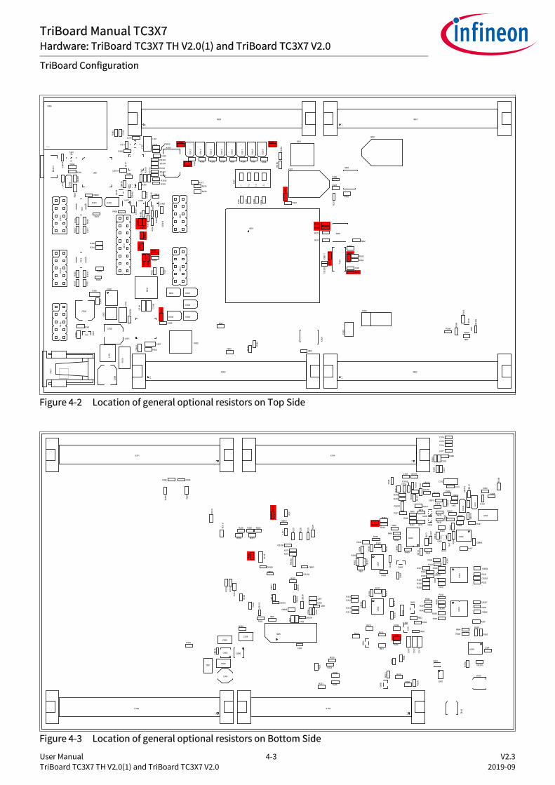
User Manual 4-3 V2.3 TriBoard TC3X7 TH V2.0(1) and TriBoard TC3X7 V2.0 2019-09
TriBoard Manual TC3X7Hardware: TriBoard TC3X7 TH V2.0(1) and TriBoard TC3X7 V2.0
TriBoard Configuration
Figure 4-2 Location of general optional resistors on Top Side
Figure 4-3 Location of general optional resistors on Bottom Side
R386
C52
2
U201
X40
6
X202
R31
09
R457
R347
R34
6X502
X403
S202
R453
R349
R34
8
R376
R375
R329
R390
R25
6
R2
55
R241
R21
7
CB
502
R509
R50
8
R507
R5
01
C50
4
C5
03
C50
1
C5
08
C5
09
C507
C502
CB5
01
L50
1
L502
U501
D508
C505U502
S502
R398
CB2
01
R213
X404
R452
R354
S501
X50
1
X401
D504 D507
D506
D505
D30
9
D30
8
D30
7
D30
6
D30
5
D30
4
D30
3
D30
2
X601
X603 X602
X30
2X3
01
T30
2T
301
U305
R35
6
R35
5
R33
6
R33
5
R53
1R439
C30
2C
301
R53
2
CB
309
R397R396R395R394R393R392
R39
1
R399
R324
R3
57R
337
Y20
1
R20
7
R206
C202
C201
R202
R203
R201
R42
8
R427
R42
6
R42
5
R42
4
R344
CB402
R402
R403
CB4
08
Y401
U401
U4
04
CB4
01
R40
1
D402
L401
BU40
1
R411
C40
2 CB
405
R42
3
R429
R430
D401
CB414
CB
415
CB
416
CB
417
CB
418
CB
419
R44
4
R4
46
R45
4
R456
R45
5
R45
1
U406U407 U408
C303
D30
1
R212
R35
9
R361
R23
0
R23
2
R23
4
R23
6
R24
0
X30
3X
304
X305
X201
R205
R204
CB
202
R377 S20
1
R225
R226
X402
R244
R247
R248
R24
9
X604
Y30
1
U307
L301
CB319
CB318
C318
C309
C311
CB317
X306
C310
C3
06
C32
0
R38
3
R3108
R3104
R3102R3101R3100
R382
Q30
1 R379R380
R31
03
CB409
U503CB5
06
C506C521
C520
L503
Q506
C518
R260
R25
9
R258
R25
7
L20
1
CB209
CB208
R374R373
R325
R327
R313
R525
R438
R437
R436
R328
R326
R312
R239
R23
7
R23
5
R23
3 R23
1
R21
9
R21
8
R503
D502
C51
1
C51
2
D501
Q501
Q50
5
R5
06
R50
2
C51
0
R50
4
R505
D503
R520
CB510
R209
R21
6
R320
C408C40
7
CB203
C5
19
R353
R352
R333
R33
4
R332
U30
4U
303
R351
R35
0
R358
R331
R330
R33
8
R30
4
R30
3
CB308
CB307
CB306
CB305
CB304
CB303
R342
R302
U30
2U
301
X701 X704
X703X702
Q 503
Q50
4
Q502
R510 R512
R511
C51
5
R536
R535
CB204
R513
R53
4
R538
R317
R307
R537
CB520
CB519
CB5
18C
B51
7
CB
516
CB
515
CB
513
CB512
CB205
CB
302
CB30
1
R343
R323
R533
R52
4
R221
R220
R22
2
R322
R321
R340
R341
R311
R301
R522
R31
9
R31
8
R3
16R
315
R3
09
R3
08
R306
R30
5
CB4
04
CB406
R405
R40
6
U402
R407
CB4
03
CB
407
R409
R41
0
R415
R416R417
R418
R414
R420
C406
R41
2Q401
Q402
U403
R42
1
R422
C404
C405
CB41
0
CB411
CB4
12
R441
R442
R45
0
C401 R404
D403
C4
03C
B41
3
L402
U405
R413
R443
R445
R447
R448
R449
C304
CB310
CB2
06
R21
1
R3
60
R362
R363
R364
R365
R223
R238
R521
U306
X405
R21
4R21
5
R40
8
R20
8
R254
R253 R251
R250 R252
R314
R381
R4
31
RN
302
R523
R433
C203
C204
C205
C206
C207
C208
R245
R246
RN301
CB316
CB315
CB314
CB313
CB312
CB311
R370
R38
5R
384
R389
C308
C30
7
C305
Q403
C312
C313
C314
C315
C316
C317
C319
R31
11 R31
10R3
107
R31
06
R3105
R440R419
R372
R371
R31
0R37
8
R3
88

User Manual 4-4 V2.3 TriBoard TC3X7 TH V2.0(1) and TriBoard TC3X7 V2.0 2019-09
TriBoard Manual TC3X7Hardware: TriBoard TC3X7 TH V2.0(1) and TriBoard TC3X7 V2.0
TriBoard Configuration
4.2.2 Resistors for peripherals
Table 4-3 Resistors for peripherals (default assembly in brackets)
Component Description
R220 Connect V_VR with VDDM (assembled)
R221 Connect +3V3 with VDDM (not assembled)
R222 Connect VAREF1 with VDDM (assembled)
R223 Connect VAREF2 with VDDM (assembled)
R301 Connect P20.7 with RXD of CAN0 transceiver (assembled)
R302 Connect P20.8 with TXD of CAN0 transceiver (assembled)
R303 Connect P14.1 with RXD of CAN0 transceiver (not assembled)
R304 Connect P14.0 with TXD of CAN0 transceiver (not assembled)
R311 Connect P23.0 with RXD of CAN1 transceiver (assembled)
R312 Connect P23.1 with TXD of CAN1 transceiver (assembled)
R313 Connect P00.1 with RXD of CAN1 transceiver (not assembled)
R314 Connect P00.0 with TXD of CAN1 transceiver (not assembled)
R320 Connect P14.10 with TXD of ERAY-A transceiver (assembled)
R321 Connect P14.9 with TXDEN of ERAY-A transceiver (assembled)
R322 Connect P14.8 with RXD of ERAY-A transceiver (assembled)
R323 Connect P32.3 with EN of ERAY-A transceiver (assembled)
R324 Connect P32.2 with ERRN of ERAY-A transceiver (assembled)
R325 Connect P02.1 with RXD of ERAY-A transceiver (not assembled)
R326 Connect P02.4 with TXDEN of ERAY-A transceiver (not assembled)
R327 Connect P02.0 with TXD of ERAY-A transceiver (not assembled)
R328 Connect P10.2 with EN of ERAY-A transceiver (not assembled)
R329 Connect P10.1 with ERRN of ERAY-A transceiver (not assembled)
R340 Connect P14.5 with TXD of ERAY-B transceiver (assembled)
R341 Connect P14.6 with TXDEN of ERAY-B transceiver (assembled)
R342 Connect P14.7 with RXD of ERAY-B transceiver (assembled)
R343 Connect P20.10 with EN of ERAY-B transceiver (assembled)
R344 Connect P20.9 with ERRN of ERAY-B transceiver (assembled)
R348 Connect P15.4 with SCL of I2C Eeprom (assembled)
R349 Connect P15.5 with SDA of I2C Eeprom (assembled)
R364 Connect P15.1 with RXD of LIN1 transceiver (assembled)
R365 Connect P15.0 with TXD of LIN1 transceiver (assembled)
R310 Connect P11.5 with CLOCKOUT of Ethernet PHY (assembled)
R370 Connect P11.12 with RXC of Ethernet PHY (assembled)
R371 Connect CLKOUT of Ethernet PHY with TXC of Ethernet PHY (not assembled)
R372 Connect P11.11 with RXCTL of Ethernet PHY (assembled)
R373 Connect P11.4 with TXC of Ethernet PHY (assembled)

User Manual 4-5 V2.3 TriBoard TC3X7 TH V2.0(1) and TriBoard TC3X7 V2.0 2019-09
TriBoard Manual TC3X7Hardware: TriBoard TC3X7 TH V2.0(1) and TriBoard TC3X7 V2.0
TriBoard Configuration
Note: All resistors are red marked in the following figures
Figure 4-4 Location of peripheral resistors on Top Side
R374 Connect P11.6 with TXCTL of Ethernet PHY (assembled)
R375 Connect P12.1 with MDIO of Ethernet PHY (assembled)
R376 Connect P12.0 with MDC of Ethernet PHY (assembled)
R377 Connect P15.8 with MDINT of Ethernet PHY (not assembled)
RN301 Connect P11.7...10 with RDX3...0 of Ethernet PHY (assembled)
RN302 Connect P11.0...3 with TDX3...0 of Ethernet PHY (assembled)
R436 Connect P14.0 with RXD of USB to UART (assembled)
R437 Connect P14.1 with TXD of USB to UART (assembled)
R438 Connect P15.2 with RXD of USB to UART (not assembled)
R440 Connect P15.3 with TXD of USB to UART (not assembled)
Table 4-3 Resistors for peripherals (default assembly in brackets) (continued)
Component Description
R386
C52
2
U201
X40
6
X202
R31
09
R457
R347
R34
6X502
X403
S202
R453
R349
R34
8
R376
R375
R329
R390
R25
6
R2
55
R241
R21
7
CB
502
R509
R50
8
R507
R5
01
C50
4
C5
03
C50
1
C5
08
C5
09
C507
C502
CB5
01
L50
1
L502
U501
D508
C505U502
S502
R398
CB2
01
R213
X404
R452
R354
S501
X50
1
X401
D504 D507
D506
D505
D30
9
D30
8
D30
7
D30
6
D30
5
D30
4
D30
3
D30
2
X601
X603 X602
X30
2X3
01
T30
2T
301
U305
R35
6
R35
5
R33
6
R33
5
R53
1
R439
C30
2C
301
R53
2
CB
309
R397R396R395R394R393R392
R39
1
R399
R324
R3
57R
337
Y20
1
R20
7
R206
C202
C201
R202
R203
R201
R42
8
R427
R42
6
R42
5
R42
4
R344
CB402
R402
R403
CB4
08
Y401
U401
U4
04
CB4
01
R40
1
D402
L401
BU40
1
R411
C40
2 CB
405
R42
3
R429
R430
D401
CB414
CB
415
CB
416
CB
417
CB
418
CB
419
R44
4
R4
46
R45
4
R456
R45
5
R45
1
U406
U407 U408
C303
D30
1
R212
R35
9
R361
R23
0
R23
2
R23
4
R23
6
R24
0
X30
3X
304
X305
X201
R205
R204
CB
202
R377 S20
1
R225
R226
X402
R244
R247
R248
R24
9
X604
Y30
1
U307
L301
CB319
CB318
C318
C309
C311
CB317
X306
C310
C3
06
C32
0
R38
3
R3108
R3104
R3102R3101R3100
R382
Q30
1 R379R380
R31
03

User Manual 4-6 V2.3 TriBoard TC3X7 TH V2.0(1) and TriBoard TC3X7 V2.0 2019-09
TriBoard Manual TC3X7Hardware: TriBoard TC3X7 TH V2.0(1) and TriBoard TC3X7 V2.0
TriBoard Configuration
Figure 4-5 Location of peripheral resistors on Bottom Side
CB409
U503CB5
06
C506C521
C520
L503
Q506
C518
R260
R25
9
R258
R25
7
L20
1
CB209
CB208
R374R373
R325
R327
R313R5
25
R438
R437
R436
R328
R326
R312
R239
R23
7
R23
5
R23
3 R23
1
R21
9
R21
8
R503
D502
C51
1
C51
2
D501
Q501
Q50
5
R5
06
R50
2
C51
0
R50
4
R505
D503
R520
CB510
R209
R21
6
R320
C408C40
7
CB203
C5
19
R353
R352
R333
R33
4
R332
U30
4U
303
R351
R35
0
R358
R331
R330
R33
8
R30
4
R30
3
CB308
CB307
CB306
CB305
CB304
CB303
R342
R302
U30
2U
301
X701 X704
X703X702
Q 503
Q50
4
Q502
R510 R512
R511
C51
5
R536
R535
CB204
R513
R53
4
R538
R317
R307
R537
CB520
CB519
CB5
18C
B51
7
CB
516
CB
515
CB
513
CB512
CB205
CB
302
CB30
1
R343
R323
R533
R52
4
R221
R220R
222
R322
R321
R340
R341
R311
R301
R522
R31
9
R31
8
R3
16R
315
R3
09
R3
08
R306
R30
5
CB4
04
CB406
R405
R40
6
U402
R407
CB4
03
CB
407
R409
R41
0
R415
R416R417
R418
R414
R420
C406
R41
2Q401
Q402
U403
R42
1
R422
C404
C405
CB41
0
CB411
CB4
12
R441
R442
R45
0
C401 R404
D403
C4
03C
B41
3
L402
U405
R413
R443
R445
R447
R448
R449
C304
CB310
CB2
06
R21
1
R3
60
R362
R363
R364
R365
R223
R238
R521
U306
X405
R21
4R21
5
R40
8
R20
8
R254
R253 R251
R250 R252
R314
R381
R4
31
RN
302
R523
R433
C203
C204
C205
C206
C207
C208
R245
R246
RN301
CB316
CB315
CB314
CB313
CB312
CB311
R370
R38
5R
384
R389
C308
C30
7
C305
Q403
C312
C313
C314
C315
C316
C317
C319
R31
11 R31
10R3
107
R31
06
R3105
R440R419
R372
R371
R31
0R37
8
R3
88
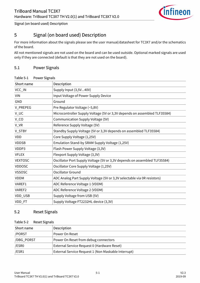
User Manual 5-1 V2.3 TriBoard TC3X7 TH V2.0(1) and TriBoard TC3X7 V2.0 2019-09
TriBoard Manual TC3X7Hardware: TriBoard TC3X7 TH V2.0(1) and TriBoard TC3X7 V2.0
Signal (on board used) Description
5 Signal (on board used) DescriptionFor more information about the signals please see the user manual/datasheet for TC3X7 and/or the schematicsof the board.All not mentioned signals are not used on the board and can be used outside. Optional marked signals are usedonly if they are connected (default is that they are not used on the board).
5.1 Power Signals
5.2 Reset Signals
Table 5-1 Power Signals
Short name Description
VCC_IN Supply Input (3,5V...40V)
VIN Input Voltage of Power Supply Device
GND Ground
V_PREPEG Pre Regulator Voltage (~5,8V)
V_UC Microcontroller Supply Voltage (5V or 3,3V depends on assembled TLF35584)
V_CO Communication Supply Voltage (5V)
V_VR Reference Supply Voltage (5V)
V_STBY Standby Supply Voltage (5V or 3,3V depends on assembled TLF35584)
VDD Core Supply Voltage (1,25V)
VDDSB Emulation Stand-by SRAM Supply Voltage (1,25V)
VDDP3 Flash Power Supply Voltage (3,3V)
VFLEX Flexport Supply Voltage (3,3V)
VEXTOSC Oscillator Port Supply Voltage (5V or 3,3V depends on assembled TLF35584)
VDDOSC Oscillator Core Supply Voltage (1,25V)
VSSOSC Oscillator Ground
VDDM ADC Analog Part Supply Voltage (5V or 3,3V selectable via 0R resistors)
VAREF1 ADC Reference Voltage 1 (VDDM)
VAREF2 ADC Reference Voltage 2 (VDDM)
VDD_USB Supply Voltage from USB (5V)
VDD_FT Supply Voltage FT2232HL device (3,3V)
Table 5-2 Reset Signals
Short name Description
/PORST Power On Reset
/DBG_PORST Power On Reset from debug connectors
/ESR0 External Service Request 0 (Hardware Reset)
/ESR1 External Service Request 1 (Non Maskable Interrupt)

User Manual 5-2 V2.3 TriBoard TC3X7 TH V2.0(1) and TriBoard TC3X7 V2.0 2019-09
TriBoard Manual TC3X7Hardware: TriBoard TC3X7 TH V2.0(1) and TriBoard TC3X7 V2.0
Signal (on board used) Description
5.3 Config Signals
5.4 Clock Signals
5.5 Debug Signals
Table 5-3 Config Signals
Short name Description
P14.5 HWCFG1 (EVR33OFF / EVR33ON)
P14.2 HWCFG2 (EVRCOFF / EVRCON)
P14.4 HWCFG6 (Pins in tristate / Pins with pull-up)
P14.3 HWCFG3 (Boot from pins / Boot from Flash BMI)
P10.5 HWCFG4 (see boot configuration Table 4-1)
P10.6 HWCFG5 (see boot configuration Table 4-1)
Table 5-4 Clock Signals
Short name Description
XTAL1 Crystal Oscillator Input
XTAL2 Crystal Oscillator Output
Table 5-5 Debug Signals
Short name Description
/TRST Test Reset
DAP0 Device Access Port Line 0 / Test Data Clock (TCK)
DAP1 Device Access Port Line 1 / Test Data Select (TMS)
DAP2 Device Access Port Line 2 / Test Data Output (TDO)
DAPE0 Device Access Port Line 0 (Emulation part)
DAPE1 Device Access Port Line 1 (Emulation part)
DAPE2 Device Access Port Line 2 (Emulation part)
P21.6 Test Data Input (TDI)
DAP0_A DAP0 / DAPE0 / TCK from debug connectors
DAP1_A DAP1 / DAPE1 / TMS from debug connectors
P21.7 DAP2 / DAPE2 / TDO from debug connectors
P33.6 Device Access Port Line 0 (standby controller)
P33.7 Device Access Port Line 1 (standby controller)
P20.2 Test Mode Select Input
P20.1 TriCore Breakpoint Input
P20.0 TriCore Breakpoint Output
AGBT_CLK_P/_N AGBT Clock Input
AGBT_TX0_P/_N AGBT Transmit Output
AGBT_ERR AGBT Error Output

User Manual 5-3 V2.3 TriBoard TC3X7 TH V2.0(1) and TriBoard TC3X7 V2.0 2019-09
TriBoard Manual TC3X7Hardware: TriBoard TC3X7 TH V2.0(1) and TriBoard TC3X7 V2.0
Signal (on board used) Description
5.6 Peripheral Signals
Table 5-6 Peripheral Signals
Short name Description
P14.1 ASCLIN0 Receive Input ACAN01 Receive Input B (optional)
P14.0 ASCLIN0 Transmit OutputCAN01 Transmit Output (optional)
P15.3 ASCLIN0 Receive Input B (optional)
P15.2 ASCLIN0 Transmit Output (optional)
P15.1 ASCLIN1 Receive Input A
P15.0 ASCLIN1 Transmit Output
P15.4 I2C0 Serial Clock
P15.5 I2C0 Serial Data Input C und Output
P20.7 CAN00 Receive Input B
P20.8 CAN00 Transmit Output
P23.0 CAN10 Receive Input C
P23.1 CAN10 Transmit Output
P00.1 CAN10 Receive Input A (optional)
P00.0 CAN10 Transmit Output (optional)
P14.10 E-Ray Channel A Transmit Data Output
P14.9 E-Ray Channel A Transmit Data Output enable
P14.8 E-Ray Channel A Receive Data Input 0
P32.3 E-Ray Channel A Enable Output
P32.2 E-Ray Channel A Error Input
P14.5 E-Ray Channel B Transmit Data Output
P14.6 E-Ray Channel B Transmit Data Output enable
P14.7 E-Ray Channel B Receive Data Input 0
P20.10 E-Ray Channel B Enable Output
P20.9 E-Ray Channel B Error Input
P02.0 E-Ray Channel A Transmit Data Output (optional)
P02.4 E-Ray Channel A Transmit Data Output enable (optional)
P02.1 E-Ray Channel A Receive Data Input 2 (optional)
P10.2 E-Ray Channel A Enable Output (optional)
P10.1 E-Ray Channel A Error Input (optional)
TXD3 Ethernet TXD3 Output (P11.0)
TXD2 Ethernet TXD2 Output (P11.1)
TXD1 Ethernet TXD1 Output (P11.2)
TXD0 Ethernet TXD0 Output (P11.3)
TXCLK Ethernet TXCLK Output (P11.4)
User Manual 5-4 V2.3 TriBoard TC3X7 TH V2.0(1) and TriBoard TC3X7 V2.0 2019-09
TriBoard Manual TC3X7Hardware: TriBoard TC3X7 TH V2.0(1) and TriBoard TC3X7 V2.0
Signal (on board used) Description
REFCLK Ethernet GREFCLK Input (P11.5)
TCTL Ethernet TCTL Output (P11.6)
RXD3 Ethernet RXD3 Input A (P11.7)
RXD2 Ethernet RXD2 Input A (P11.8)
RXD1 Ethernet RXD1 Input A (P11.9)
RXD0 Ethernet RXD0 Input A (P11.10)
RCTL Ethernet RCTL Input A (P11.11)
RXCLK Ethernet RXCLK Input A (P11.12)
P12.0 Ethernet Management Data Clock Output (MDC)
P12.1 Ethernet Management Data Input/Output (MDIO)
P15.8 Ethernet MD Interrupt Input (optional)
P14.2 QSPI2 Slave Select Output 1 for SCS of TLF35584
P15.3 QSPI2 Master Clock Output for SCL of TLF35584
P15.6 QSPI2 Master Transmit Output for SDI of TLF35584
P15.7 QSPI2 Master Receive Input B for SDO from TLF35584
P14.3 Output for Watchdog Input of TLF35584
P33.8 SMU_FSP0 Output for Error Signal Input of TLF35584
P33.9 Input for Safe State Signal 1 from TLF35584
P33.10 Output for Wake/Inhibit Input of TLF35584
P20.0 HSCT0/1 System Clock
RXD0_N HSCT0 Data Negative Input (P21.2)
RXD0_P HSCT0 Data Positive Input (P21.3)
TXD0_N HSCT0 Data Negative Output (P21.4)
TXD0_P HSCT0 Data Positive Output (P21.5
RXD1_N HSCT1 Data Negative Input (P21.0)
RXD1_P HSCT1 Data Positive Input (P21.1)
TXD1_N HSCT1 Data Negative Output (P22.2)
TXD1_P HSCT1 Data Positive Output (P22.3
P20[11...14] On board LED’s
P33[4...7] On board LED’s (standby voltage supplied)
Table 5-6 Peripheral Signals (continued)
Short name Description

User Manual 6-1 V2.3 TriBoard TC3X7 TH V2.0(1) and TriBoard TC3X7 V2.0 2019-09
TriBoard Manual TC3X7Hardware: TriBoard TC3X7 TH V2.0(1) and TriBoard TC3X7 V2.0
Connector Pin Assignment
6 Connector Pin AssignmentThe TriBoard will be shipped with four male (plug) connectors on top layer and four female (socket) connectorson bottom layer. The default connectors are 80-pol. Board to Board connectors from Samtec:
http://www.samtec.com
Plug:FTSH-140-02-L-DV-ES-A
Socket:FLE-140-01-G-DV-A
6.1 On Board only used signalsFollowing port pins are only used on board and are not connected to any connector also not via resistor:
Table 6-1 On Board only used Signals
Short name Description
P32.0 Used as VGATE1N/VCAP0 for EVRC
P32.1 Used as VGATE1P/VCAP1 for EVRC
P14.2 Used as HWCFG2 and Slave Select Output (SLSO21) to TLF35584
P14.4 Used as HWCFG6 and Output to Watchdog Input of TLF35584
P14.5 Used as HWCFG1 and E-Ray Channel B Transmit Data Output
P14.6 Used as E-Ray Channel B Transmit Data Output enable
P11.0 Used as Gigabit Transmit Data Output 3 for RGMII
P11.1 Used as Gigabit Transmit Data Output 2 for RGMII
P11.2 Used as Gigabit Transmit Data Output 1 for RGMII
P11.3 Used as Gigabit Transmit Data Output 0 for RGMII
P11.4 Used as Gigabit Transmit Clock Output for RGMII
P11.5 Used as Gigabit Reference Clock input for RGMII (125 MHz high precision)
P11.6 Used as Gigabit Transmit Control Output for RGMII
P11.7 Used as Gigabit Receive Data Input 3 for RGMII
P11.8 Used as Gigabit Receive Data Input 2 for RGMII
P11.9 Used as Gigabit Receive Data Input 1 for RGMII
P11.10 Used as Gigabit Receive Data Input 0 for RGMII
P11.11 Used as Gigabit Receive Data Control Input for RGMII
P11.12 Used as Gigabit Receive Clock Input for RGMII
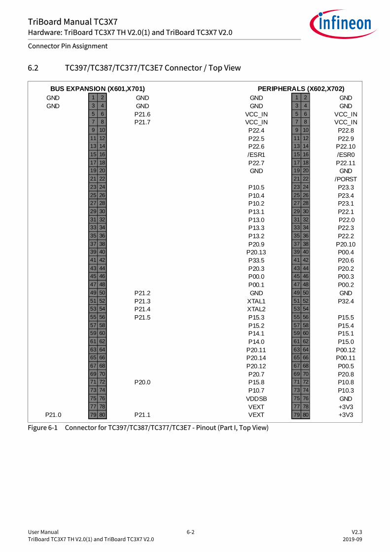
User Manual 6-2 V2.3 TriBoard TC3X7 TH V2.0(1) and TriBoard TC3X7 V2.0 2019-09
TriBoard Manual TC3X7Hardware: TriBoard TC3X7 TH V2.0(1) and TriBoard TC3X7 V2.0
Connector Pin Assignment
6.2 TC397/TC387/TC377/TC3E7 Connector / Top View
Figure 6-1 Connector for TC397/TC387/TC377/TC3E7 - Pinout (Part I, Top View)
GND 1 2 GND GND 1 2 GNDGND 3 4 GND GND 3 4 GND
5 6 P21.6 VCC_IN 5 6 VCC_IN7 8 P21.7 VCC_IN 7 8 VCC_IN9 10 P22.4 9 10 P22.8
11 12 P22.5 11 12 P22.913 14 P22.6 13 14 P22.1015 16 /ESR1 15 16 /ESR017 18 P22.7 17 18 P22.1119 20 GND 19 20 GND21 22 21 22 /PORST23 24 P10.5 23 24 P23.325 26 P10.4 25 26 P23.427 28 P10.2 27 28 P23.129 30 P13.1 29 30 P22.131 32 P13.0 31 32 P22.033 34 P13.3 33 34 P22.335 36 P13.2 35 36 P22.237 38 P20.9 37 38 P20.1039 40 P20.13 39 40 P00.441 42 P33.5 41 42 P20.643 44 P20.3 43 44 P20.245 46 P00.0 45 46 P00.347 48 P00.1 47 48 P00.249 50 P21.2 GND 49 50 GND51 52 P21.3 XTAL1 51 52 P32.453 54 P21.4 XTAL2 53 5455 56 P21.5 P15.3 55 56 P15.557 58 P15.2 57 58 P15.459 60 P14.1 59 60 P15.161 62 P14.0 61 62 P15.063 64 P20.11 63 64 P00.1265 66 P20.14 65 66 P00.1167 68 P20.12 67 68 P00.569 70 P20.7 69 70 P20.871 72 P20.0 P15.8 71 72 P10.873 74 P10.7 73 74 P10.375 76 VDDSB 75 76 GND77 78 VEXT 77 78 +3V3
P21.0 79 80 P21.1 VEXT 79 80 +3V3
BUS EXPANSION (X601,X701) PERIPHERALS (X602,X702)

User Manual 6-3 V2.3 TriBoard TC3X7 TH V2.0(1) and TriBoard TC3X7 V2.0 2019-09
TriBoard Manual TC3X7Hardware: TriBoard TC3X7 TH V2.0(1) and TriBoard TC3X7 V2.0
Connector Pin Assignment
Figure 6-2 Connector for TC397/TC387/TC377/TC3E7 - Pinout (Part II, Top View)
GND 1 2 GND GND 1 2 GNDGND 3 4 GND GND 3 4 GNDAN0 5 6 AN16 P00.9 5 6 P11.14AN1 7 8 AN17 P00.10 7 8 P11.15AN2 9 10 AN18 P02.0 9 10AN3 11 12 AN19 P02.1 11 12AN4 13 14 AN20 P02.2 13 14AN5 15 16 AN21 P02.3 15 16AN6 17 18 AN22 P02.4 17 18 P14.7AN7 19 20 AN23 P02.5 19 20 P14.8AN8 21 22 AN24 P02.9 21 22 P14.9AN9 23 24 AN25 P02.10 23 24 P14.10
AN10 25 26 AN26 P02.11 25 26 P15.6AN11 27 28 AN27 P01.3 27 28 P15.7AN12 29 30 AN28 P01.4 29 30 P20.1AN13 31 32 AN29 P10.0 31 32 P01.5AN14 33 34 AN30 P10.1 33 34 P01.6AN15 35 36 AN31 P10.6 35 36 P23.0GND 37 38 GND P12.0 37 38 P23.2
VDDM 39 40 VAREF1 P12.1 39 40 P23.5GND 41 42 VAREF2 41 42 P23.6GND 43 44 GND 43 44 P23.7AN32 45 46 AN40 45 46AN33 47 48 AN41 47 48AN34 49 50 AN42 49 50 P32.2AN35 51 52 AN43 51 52 P32.3AN36 53 54 AN44 53 54 P32.5AN37 55 56 AN45 55 56 P33.8AN38 57 58 AN46 57 58 P33.9AN39 59 60 AN47 59 60 P33.10GND 61 62 GND 61 62 P33.13P33.3 63 64 P33.6 63 64 P33.14P33.2 65 66 P33.0 65 66 P33.15P33.1 67 68 P33.4 P11.13 67 68 P32.6VEXT 69 70 +3V3 P34.1 69 70 P32.7P02.6 71 72 P00.6 P34.2 71 72 P34.4P02.7 73 74 P00.7 P34.3 73 74 P34.5P02.8 75 76 P00.8 VFLEX 75 76 P01.7P33.7 77 78 P14.3 VEXT 77 78 +3V3P33.11 79 80 P33.12 VEXT 79 80 +3V3
ADC (X603, X703) GTM / PORTS (X604,X704)

User Manual 6-4 V2.3 TriBoard TC3X7 TH V2.0(1) and TriBoard TC3X7 V2.0 2019-09
TriBoard Manual TC3X7Hardware: TriBoard TC3X7 TH V2.0(1) and TriBoard TC3X7 V2.0
Connector Pin Assignment
6.3 TC367 Connector / Top View
Figure 6-3 Connector for TC367 - Pinout (Part I, Top View)
GND 1 2 GND GND 1 2 GNDGND 3 4 GND GND 3 4 GND
5 6 P21.6 VCC_IN 5 6 VCC_IN7 8 P21.7 VCC_IN 7 8 VCC_IN9 10 9 10
11 12 11 1213 14 13 1415 16 /ESR1 15 16 /ESR017 18 17 1819 20 GND 19 20 GND21 22 21 22 /PORST23 24 P10.5 23 24 P23.325 26 P10.4 25 26 P23.427 28 P10.2 27 28 P23.129 30 P13.1 29 30 P22.131 32 P13.0 31 32 P22.033 34 P13.3 33 34 P22.335 36 P13.2 35 36 P22.237 38 P20.9 37 38 P20.1039 40 P20.13 39 40 P00.441 42 P33.5 41 42 P20.643 44 P20.3 43 44 P20.245 46 P00.0 45 46 P00.347 48 P00.1 47 48 P00.249 50 P21.2 GND 49 50 GND51 52 P21.3 XTAL1 51 52 P32.453 54 P21.4 XTAL2 53 5455 56 P21.5 P15.3 55 56 P15.557 58 P15.2 57 58 P15.459 60 P14.1 59 60 P15.161 62 P14.0 61 62 P15.063 64 P20.11 63 64 P00.1265 66 P20.14 65 66 P00.1167 68 P20.12 67 68 P00.569 70 P20.7 69 70 P20.871 72 P20.0 P15.8 71 72 P10.873 74 P10.7 73 74 P10.375 76 VDDSB 75 76 GND77 78 VEXT 77 78 +3V3
P21.0 79 80 P21.1 VEXT 79 80 +3V3
BUS EXPANSION (X601,X701) PERIPHERALS (X602,X702)

User Manual 6-5 V2.3 TriBoard TC3X7 TH V2.0(1) and TriBoard TC3X7 V2.0 2019-09
TriBoard Manual TC3X7Hardware: TriBoard TC3X7 TH V2.0(1) and TriBoard TC3X7 V2.0
Connector Pin Assignment
Figure 6-4 Connector for TC367 - Pinout (Part II, Top View)
GND 1 2 GND GND 1 2 GNDGND 3 4 GND GND 3 4 GNDAN0 5 6 AN16 P00.9 5 6 P11.14AN1 7 8 AN17 P00.10 7 8 P11.15AN2 9 10 AN18 P02.0 9 10AN3 11 12 AN19 P02.1 11 12AN4 13 14 AN20 P02.2 13 14AN5 15 16 AN21 P02.3 15 16AN6 17 18 AN22 P02.4 17 18 P14.7AN7 19 20 AN23 P02.5 19 20 P14.8AN8 21 22 AN24 21 22 P14.9AN9 23 24 AN25 23 24 P14.10
AN10 25 26 AN26 25 26 P15.6AN11 27 28 AN27 27 28 P15.7AN12 29 30 AN28 29 30 P20.1AN13 31 32 AN29 P10.0 31 32AN14 33 34 AN30 P10.1 33 34AN15 35 36 AN31 P10.6 35 36 P23.0GND 37 38 GND P12.0 37 38 P23.2
VDDM 39 40 VAREF1 P12.1 39 40 P23.5GND 41 42 41 42GND 43 44 GND 43 44AN32 45 46 AN40 45 46AN33 47 48 AN41 47 48AN34 49 50 AN42 49 50 P32.2AN35 51 52 AN43 51 52 P32.3AN36 53 54 AN44 53 54AN37 55 56 AN45 55 56 P33.8AN38 57 58 AN46 57 58 P33.9AN39 59 60 AN47 59 60 P33.10GND 61 62 GND 61 62 P33.13P33.3 63 64 P33.6 63 64P33.2 65 66 P33.0 65 66P33.1 67 68 P33.4 P11.13 67 68VEXT 69 70 +3V3 69 70P02.6 71 72 P00.6 71 72P02.7 73 74 P00.7 73 74P02.8 75 76 P00.8 VFLEX 75 76P33.7 77 78 P14.3 VEXT 77 78 +3V3P33.11 79 80 P33.12 VEXT 79 80 +3V3
ADC (X603, X703) GTM / PORTS (X604,X704)

User Manual 6-6 V2.3 TriBoard TC3X7 TH V2.0(1) and TriBoard TC3X7 V2.0 2019-09
TriBoard Manual TC3X7Hardware: TriBoard TC3X7 TH V2.0(1) and TriBoard TC3X7 V2.0
Connector Pin Assignment
6.4 TC337/TC327 Connector / Top View
Figure 6-5 Connector for TC337/TC327 - Pinout (Part I, Top View)
GND 1 2 GND GND 1 2 GNDGND 3 4 GND GND 3 4 GND
5 6 P21.6 VCC_IN 5 6 VCC_IN7 8 P21.7 VCC_IN 7 8 VCC_IN9 10 P22.4 9 10
11 12 11 1213 14 13 1415 16 /ESR1 15 16 /ESR017 18 17 1819 20 GND 19 20 GND21 22 21 22 /PORST23 24 P10.5 23 2425 26 P10.4 25 2627 28 P10.2 27 28 P23.129 30 P13.1 29 30 P22.131 32 P13.0 31 32 P22.033 34 P13.3 33 34 P22.335 36 P13.2 35 36 P22.237 38 P20.9 37 38 P20.1039 40 P20.13 39 40 P00.441 42 P33.5 41 42 P20.643 44 P20.3 43 44 P20.245 46 P00.0 45 46 P00.347 48 P00.1 47 48 P00.249 50 P21.2 GND 49 50 GND51 52 P21.3 XTAL1 51 52 P32.453 54 P21.4 XTAL2 53 5455 56 P21.5 P15.3 55 56 P15.557 58 P15.2 57 58 P15.459 60 P14.1 59 60 P15.161 62 P14.0 61 62 P15.063 64 P20.11 63 64 P00.1265 66 P20.14 65 66 P00.1167 68 P20.12 67 68 P00.569 70 P20.7 69 70 P20.871 72 P20.0 P15.8 71 72 P10.873 74 P10.7 73 74 P10.375 76 VDDSB 75 76 GND77 78 VEXT 77 78 +3V3
P21.0 79 80 P21.1 VEXT 79 80 +3V3
BUS EXPANSION (X601,X701) PERIPHERALS (X602,X702)

User Manual 6-7 V2.3 TriBoard TC3X7 TH V2.0(1) and TriBoard TC3X7 V2.0 2019-09
TriBoard Manual TC3X7Hardware: TriBoard TC3X7 TH V2.0(1) and TriBoard TC3X7 V2.0
Connector Pin Assignment
Figure 6-6 Connector for TC337/TC327 - Pinout (Part II, Top View)
GND 1 2 GND GND 1 2 GNDGND 3 4 GND GND 3 4 GNDAN0 5 6 P00.9 5 6AN1 7 8 P00.10 7 8AN2 9 10 P02.0 9 10AN3 11 12 P02.1 11 12AN4 13 14 P02.2 13 14AN5 15 16 P02.3 15 16AN6 17 18 P02.4 17 18 P14.7AN7 19 20 P02.5 19 20 P14.8AN8 21 22 21 22 P14.9AN9 23 24 23 24 P14.10
AN10 25 26 25 26 P15.6AN11 27 28 27 28 P15.7AN12 29 30 29 30 P20.1AN13 31 32 P10.0 31 32AN14 33 34 P10.1 33 34AN15 35 36 P10.6 35 36GND 37 38 GND 37 38
VDDM 39 40 VAREF1 39 40 P23.5GND 41 42 41 42GND 43 44 GND 43 44AN32 45 46 45 46AN33 47 48 47 48AN34 49 50 49 50AN35 51 52 51 52AN36 53 54 53 54AN37 55 56 55 56 P33.8AN38 57 58 57 58 P33.9AN39 59 60 59 60 P33.10GND 61 62 GND 61 62P33.3 63 64 P33.6 63 64P33.2 65 66 P33.0 65 66P33.1 67 68 P33.4 67 68VEXT 69 70 +3V3 69 70P02.6 71 72 P00.6 P34.2 71 72P02.7 73 74 P00.7 P34.3 73 74P02.8 75 76 P00.8 VEXT 75 76P33.7 77 78 P14.3 VEXT 77 78 +3V3P33.11 79 80 P33.12 VEXT 79 80 +3V3
ADC (X603, X703) GTM / PORTS (X604,X704)

User Manual 6-8 V2.3 TriBoard TC3X7 TH V2.0(1) and TriBoard TC3X7 V2.0 2019-09
TriBoard Manual TC3X7Hardware: TriBoard TC3X7 TH V2.0(1) and TriBoard TC3X7 V2.0
Connector Pin Assignment
6.5 Power connector pinout
Figure 6-7 Power connector pinout (Roka 520 2550
6.6 USB connector pinout
Figure 6-8 USB connector pinout (Micro USB B-type)
6.7 FlexRay™ (ERAY) connector pinout
Figure 6-9 FlexRay™ (ERAY) connector pinout (IDC10)
6.8 CAN connector pinout
Figure 6-10 CAN connector pinout (IDC10)
+3,5V...40V
GND
D+
D-
VC
C
GN
DID
2 4 6 8
GN
D
BP BM
1 3 5 7 9
10
2 4 6 8
GN
D
CA
NH
CAN
L
1 3 5 7 9
10
GN
D

User Manual 6-9 V2.3 TriBoard TC3X7 TH V2.0(1) and TriBoard TC3X7 V2.0 2019-09
TriBoard Manual TC3X7Hardware: TriBoard TC3X7 TH V2.0(1) and TriBoard TC3X7 V2.0
Connector Pin Assignment
6.9 LIN connector pinout
Figure 6-11 LIN connector pinout (IDC10)
6.10 HSCT connector pinout
Figure 6-12 HSCT connector pinout (IEE1394 6-conductor)
6.11 Ethernet connector pinout
Figure 6-13 Ethernet connector pinout (RJ45)
2 4 6 8
GN
D
BUS
VIN
opt
1 3 5 7 9
10
GN
D
3
62
TXD
_P
RXD
_P
1 5
4
GN
D
GN
D
TXD
_N
RXD
_N
SYSC
LKJ2J1 J3 J4 J5 J6 J7 J8

User Manual 6-10 V2.3 TriBoard TC3X7 TH V2.0(1) and TriBoard TC3X7 V2.0 2019-09
TriBoard Manual TC3X7Hardware: TriBoard TC3X7 TH V2.0(1) and TriBoard TC3X7 V2.0
Connector Pin Assignment
6.12 OCDS1 connector pinout
Figure 6-14 OCDS1 connector pinout (IDC16)
6.13 DAP connector pinout
Figure 6-15 DAP connector pinout (Samtec FTSH10)
TDO
2 4 6 8
1 3 5 7 9
10 12 14 16
11 13 15
TDI
/TR
ST
TCK
/BR
KIN
TMS
GN
D
GN
D
/PO
RST
/BR
KOU
T
GN
D
V_U
C
DA
P0
2 4 6 8
1 3 5 7 9
10
US
R1_
IO
/PO
RS
T
US
R0_
IO
DA
P1
GN
D
GN
D
Key
GN
D
V_U
C
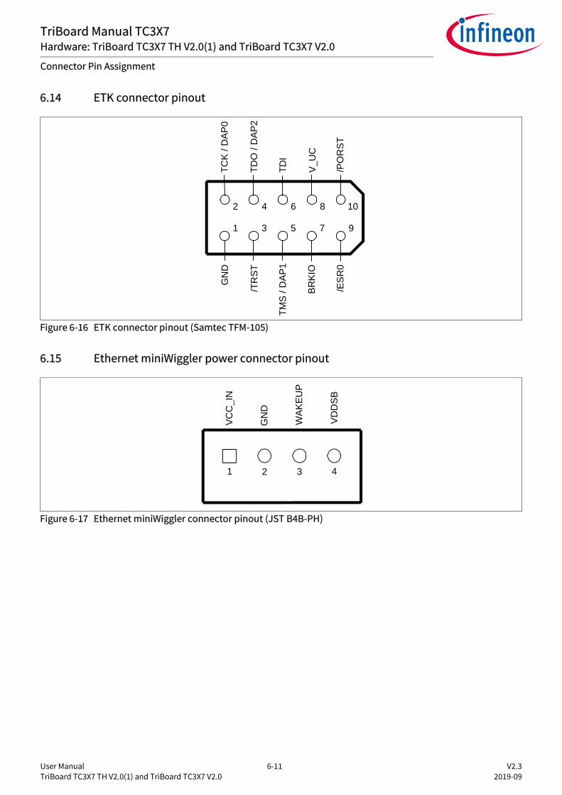
User Manual 6-11 V2.3 TriBoard TC3X7 TH V2.0(1) and TriBoard TC3X7 V2.0 2019-09
TriBoard Manual TC3X7Hardware: TriBoard TC3X7 TH V2.0(1) and TriBoard TC3X7 V2.0
Connector Pin Assignment
6.14 ETK connector pinout
Figure 6-16 ETK connector pinout (Samtec TFM-105)
6.15 Ethernet miniWiggler power connector pinout
Figure 6-17 Ethernet miniWiggler connector pinout (JST B4B-PH)
TDO
/ D
AP2
2 4 6 8
1 3 5 7 9
10
V_U
C
/PO
RST
TDI
TCK
/ D
AP0
/TR
ST
TMS
/ DA
P1
BRK
IO
/ES
R0
GN
D
2 41 3
WAK
EUP
VD
DSB
VCC
_IN
GN
D

User Manual 6-12 V2.3 TriBoard TC3X7 TH V2.0(1) and TriBoard TC3X7 V2.0 2019-09
TriBoard Manual TC3X7Hardware: TriBoard TC3X7 TH V2.0(1) and TriBoard TC3X7 V2.0
Connector Pin Assignment
6.16 AGBT connector pinout
Figure 6-18 AGBT connector pinout (Samtec ASP-137969-01)
AGBT
TX0
_N2 4 6 8
1 3 5 7 9
10 12 14 16
11 13 15D
AP1
/TR
ST
DA
P0
AG
BT
ER
R
AGBT
TX0
_P
GN
D
TGIO
x
AG
BT C
LK_P
V_U
C18 20 22
17 19 21
TDI
TDO
AGB
T C
LK_N
/PO
RS
T
GN
D
GN
D
G N DG N D
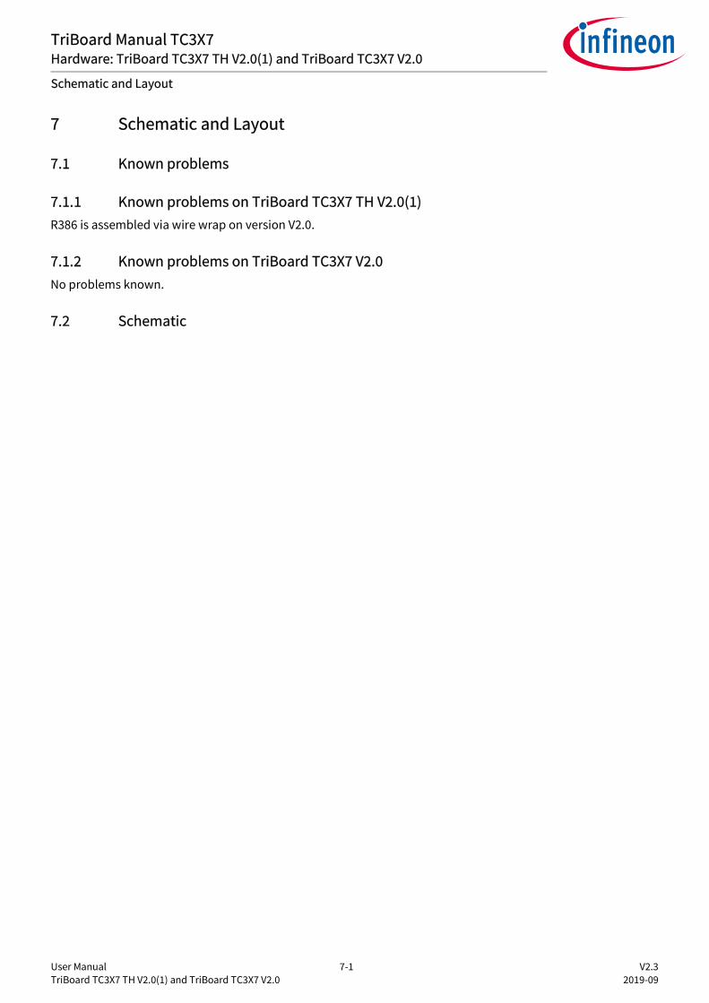
User Manual 7-1 V2.3 TriBoard TC3X7 TH V2.0(1) and TriBoard TC3X7 V2.0 2019-09
TriBoard Manual TC3X7Hardware: TriBoard TC3X7 TH V2.0(1) and TriBoard TC3X7 V2.0
Schematic and Layout
7 Schematic and Layout
7.1 Known problems
7.1.1 Known problems on TriBoard TC3X7 TH V2.0(1)R386 is assembled via wire wrap on version V2.0.
7.1.2 Known problems on TriBoard TC3X7 V2.0No problems known.
7.2 Schematic

User Manual 7-2 V2.3 TriBoard TC3X7 TH V2.0(1) and TriBoard TC3X7 V2.0 2019-09
TriBoard Manual TC3X7Hardware: TriBoard TC3X7 TH V2.0(1) and TriBoard TC3X7 V2.0
Schematic and Layout
Figure 7-1 Schematic - Project
11
22
33
44
55
66
77
88
DD
CC
BB
AA
1In
fineo
n Te
chno
logi
es A
GA
TV M
C A
CE
ATV
CES
Am
Cam
peon
1-1
2D
-855
79 N
eubi
berg
Tel.:
+49
-89-
234-
0
7
10.1
1.20
17
Num
ber:
Dat
e:
Shee
t:of
Tri
Boa
rd T
C3X
7 Pr
ojec
t
2.01
Rev
isio
n:
G:\T
echn
ical
_Sup
port
\Tri
Core
\Tri
Boar
d\ED
A_D
XP\T
riBo
ard
AURI
X 2G
\Tri
Boar
d TC
3X7\
TriB
oard
TC3
X7 V
2.X\
TriB
oard
_TC
3X7_
V20.
prj
File
:
XTA
L[1.
.2]
DEB
UG
..
POR
T[00
..34]
AN
[0..4
7]
GET
H..
Clo
ck, C
onfig
, Deb
ug, P
orts
and
AD
CC
lk_C
fg_D
bg_P
orts
_Adc
.sch
POR
T[00
..34]
/ESR
0
GET
H..O
n B
oard
Per
iphe
rals
Perip
hera
ls.sc
h
DEB
UG
..
POR
T[00
..34]
/ESR
0
/PO
RST
min
iWig
gler
and
Deb
ug C
onne
ctor
sw
iggl
er_D
bg_c
on.sc
h
/PO
RST
/ESR
0
/ESR
1
POR
T[00
..34]
Pow
er S
uppl
ySu
pply
.sch
XTA
L[1.
.2]
POR
T[00
..34]
AN
[0..4
7]
/PO
RST
/ESR
0
/ESR
1
NC
1[5.
.80]
NC
2[5.
.80]
NC
4[5.
.80]
Con
nect
or P
lug
Con
nect
m.sc
h
XTA
L[1.
.2]
POR
T[00
..34]
AN
[0..4
7]
/PO
RST
/ESR
0
/ESR
1
NC
1[5.
.80]
NC
2[5.
.80]
NC
4[5.
.80]Con
nect
or S
ocke
tC
onne
ctf.s
ch
NC4[5..80]
NC2[5..80]
NC1[5..80]
PORT[00..34]
AN
[0..4
7]
XTA
L[1.
.2]
/ESR
0
/PO
RST
/ESR
1
DEB
UG
..
GET
H..
User Manual 7-3 V2.3 TriBoard TC3X7 TH V2.0(1) and TriBoard TC3X7 V2.0 2019-09
TriBoard Manual TC3X7Hardware: TriBoard TC3X7 TH V2.0(1) and TriBoard TC3X7 V2.0
Schematic and Layout
Figure 7-2 Schematic - Clock, Config, Debug, Ports and ADC
11
22
33
44
55
66
77
88
DD
CC
BB
AA
2In
fineo
n Te
chno
logi
es A
GA
TV M
C A
CE
ATV
CES
Am
Cam
peon
1-1
2D
-855
79 N
eubi
berg
Tel.:
+49
-89-
234-
0
7
10.1
1.20
17
Num
ber:
Dat
e:
Shee
t:of
Tri
Boa
rd T
C3X
7 C
lock
, Con
fig, D
ebug
, Por
ts, A
DC
2.01
Rev
isio
n:
G:\T
echn
ical
_Sup
port
\Tri
Core
\Tri
Boar
d\ED
A_D
XP\T
riBo
ard
AURI
X 2G
\Tri
Boar
d TC
3X7\
TriB
oard
TC3
X7 V
2.X\
Clk_
Cfg
_Dbg
_Por
ts_A
dc.sc
hFi
le:
P21.6
POR
T[00
..34]
CLO
CK
& T
ESTM
OD
E
XTA
L1M
20
XTA
L2M
19
TRST
L19
TCK
/ D
AP0
J16
P21.
6 / T
DI
H17
P21.
7 / T
DO
/ D
AP2
H16
TMS
/ DA
P1K
16
VSS
OSC
L20
P20.
2 / T
ESTM
OD
EH
19
JTA
G /
DA
P / O
CD
S1
P20.
1 / T
GI1
N /
TGO
1NG
19
VD
DO
SCN
19
VEX
TOSC
N20
VSS
/ A
GB
TTX
0NP1
0V
SS /
AG
BTT
X0P
P11
VSS
/ A
GB
TCLK
NL7
VSS
/ A
GB
TER
RL1
4
VSS
/ A
GB
TCLK
PK
7N
C /
DA
PE0
K14
VSS
/ D
APE
1G
11
VSS
/ D
APE
2G
10
DA
PE /
AG
BT
(ED
onl
y)
U20
1B
TC3X
7
P15.
3 / S
CLK
2B
17
P15.
5 / S
DA
0E1
4
P20.
10E1
9
P20.
14C
20
P11.
6 / T
CTL
D9
P11.
9 / R
XD
1AA
9
P11.
3 / T
XD
0B
10
P14.
1 / A
RX
0AA
15P1
4.0
/ ATX
0B
16
P15.
1 / A
RX
1AA
18P1
5.0
/ ATX
1B
20
P20.
11E2
0
P20.
12D
19
P20.
13D
20
P20.
8 / T
XD
CA
N0
F20
P20.
9E1
7
VFL
EXD
5
P11.
12 /
RX
CLK
AB
8
P11.
10 /
RX
D0A
B9
P11.
2 / T
XD
1A
10
P15.
4 / S
CL
A17
P33.
5Y
12
P20.
7 / R
XD
CA
N0B
F19
P11.
11 /
RC
TLA
A8
P12.
0 / M
DC
E12
P12.
1 / M
DIO
E11
P11.
7 / R
XD
3AE8
P11.
1 / T
XD
2E9
P11.
8 / R
XD
2AE7
P11.
0 / T
XD
3E1
0
P11.
4 / T
XC
LKD
10P1
1.5
/ GR
EFC
LKD
8
P11.
14D
7
P11.
15D
6
P11.
13E6
ON
BO
AR
D U
SED
PER
IPH
ERA
LS /
PIN
S
P23.
0 / R
XD
CA
N4C
V20
P23.
1 / T
XD
CA
N4
U19
P14.
7 / R
XD
xBD
13P1
4.8
/ RX
DxA
A13
P14.
9 / T
XEN
xAD
12
P14.
10 /
TXD
xAD
11P1
4.5
/ HW
CFG
1 / T
XD
xBA
14P1
4.6
/ TX
ENxB
B13
P32.
3Y
19P3
2.2
Y18
P15.
7 / M
RST
2BD
15P1
5.6
/ MTS
R2
A16
P33.
7Y
13
P33.
4W
12
P33.
6W
13
ASC
LIN
CA
N
QSP
I / T
LF35
584
ERA
Y
I2C LE
Ds
P14.
4 / H
WC
FG6
B15
P14.
2 / S
LSO
21 /
HW
CFG
2E1
3
P33.
8 / S
MU
_FSP
W14
P33.
9Y
14
P21.
3 / R
XD
0PJ1
9P2
1.4
/ TX
D0N
K20
P21.
5 / T
XD
0PJ2
0
P14.
3 / H
WC
FG3
B14
P10.
5 / H
WC
FG4
B5
P10.
6 / H
WC
FG5
A4
P20.
0 / S
YSC
LKH
20P2
1.2
/ RX
D0N
K19
HSC
T
HW
CFG
P33.
10W
15
P33.
11Y
15
GIG
AB
IT E
THER
NET
BU
TTO
N
P22.
3 / T
XD
1PR
19P2
2.2
/ TX
D1N
R20
P21.
1 / R
XD
1PJ1
7P2
1.0
/ RX
D1N
K17
U20
1C
TC3X
7
P20.1
POR
T[00
..34]
P20.2
P21.
7
GN
D
R20
6op
t
XTA
L[1.
.2]
XTA
L1
XTA
L2
R20
3
50R
_opt
VSS
OSC
DEB
UG
..
R20
7
0R
C20
210
pFC
201
10pF
VSS
OSC
VSS
OSC
1 2
Y20
120
MH
z
R20
110
K
V_U
C
P20.
2R
202
opt
GN
D
XTA
L[1.
.2]
R20
4
0R R20
5
0R
R21
6
0R
DAP2
R20
9
0RC
B20
110
0nR
208
0RC
B20
210
0n
VD
D
VSS
OSC
V_U
C
VSS
OSC
VD
DO
SC
VEX
TOSC
AN
[0..4
7]
V_V
R
CB
204
470n
GN
D
VD
DM
+3V
3
FOR
5V
AD
C
FOR
3,3
V A
DC
AN
0 / E
DS3
PAT1
0
AN
1 / E
DS3
NA
U10
AN
2 / E
DS0
PAW
9
AN
3 / E
DS0
NA
U9
EVA
DC
/ ED
SAD
C
AN
4T9
AN
5Y
9
AN
6T8
AN
35R
2
AN
7U
8
AN
8W
8
AN
10Y
8
AN
11W
7
AN
12 /
EDS0
PBT7
AN
13 /
EDS0
NB
W6
AN
16W
5
AN
17 /
P40.
10U
5
AN
18 /
P40.
11W
4
AN
19 /
P40.
12W
3
AN
20 /
EDS2
PAY
3
AN
21 /
EDS2
NA
Y2
AN
24 /
EDS2
PB /
P40.
0W
2
AN
25 /
EDS2
NB
/ P4
0.1
W1
AN
26 /
P40.
2V
2
AN
44 /
EDS1
PCN
1
AN
45 /
EDS1
NC
N2
AN
46 /
EDS1
PDM
1
AN
47 /
EDS1
ND
M2
VA
GN
D1
Y7
VA
REF
1Y
6
VD
DM
Y5
VSS
MY
4
AN
27 /
P40.
3V
1
AN
28 /
P40.
13U
2
AN
29 /
P40.
14U
1
AN
32 /
P40.
4P4
AN
33 /
P40.
5R
1
AN
36 /
EDS1
PA /
P40.
6N
4
AN
37 /
EDS1
NA
/ P4
0.7
P2
AN
38 /
EDS1
PB /
P40.
8N
5
AN
39 /
EDS1
NB
/ P4
0.9
P1
VA
GN
D2
T2
VA
REF
2T1
AN
40M
5
AN
41M
4
AN
42L5
AN
43L4
AN
34P5
AN
30T4
AN
31R
4
AN
22T5
AN
23R
5
AN
14 /
EDS3
PBU
6
AN
15 /
EDS3
NB
T6
AN
9U
7
U20
1E
TC3X
7
R22
2
6R8
CB
205
2,2μ
F
GN
D
VA
REF
1V
DD
M
R22
3
6R8
CB
206
2,2μ
F
GN
D
VA
REF
2V
DD
M
R22
0
1R2
R22
1
1R2_
opt
AN
0A
N1
AN
2A
N3
AN
4A
N5
AN
6
AN
8A
N9
AN
10A
N11
AN
12A
N13
AN
14A
N15
AN
16A
N17
AN
18A
N19
AN
22A
N23
AN
24A
N25
AN
26A
N27
AN
28A
N29
AN
30
AN
32A
N33
AN
34A
N35
AN
36A
N37
AN
38A
N39
AN
40A
N41
AN
42A
N43
AN
46
POR
TS
P23.
4T2
0
P13.
1A
12P1
3.0
B12
P13.
3A
11
P10.
0A
7
P13.
2B
11
P10.
7A
3
P10.
8B
4
P23.
5T1
7
P22.
0P2
0
P22.
1P1
9
P32.
4W
18
P15.
8D
14
P33.
12W
16
P33.
13Y
16
P23.
3T1
9
P00.
10K
5
P33.
0W
10
P00.
9K
2
P10.
4B
6P1
0.3
A6
P10.
2A
5P1
0.1
B7
P33.
1Y
10
P33.
2W
11
P33.
3Y
11
P33.
14T1
4
P33.
15U
14
P02.
9E4
P02.
10F5
P02.
11F4
P01.
3G
5
P01.
4G
4
P01.
5H
5
P01.
6H
4
P01.
7J5
P32.
6U
15
P34.
1U
11
P34.
2T1
2
P34.
3U
12
P34.
4T1
3
P34.
5U
13
P32.
7U
16
P32.
5T1
5
P23.
6R
17
P23.
7R
16
P22.
4P1
6
P22.
5P1
7
P22.
6N
16
P22.
7N
17
P22.
8M
16
P22.
9M
17
P22.
10L1
6
P22.
11L1
7
P02.
0B
1
P02.
1C
2
P02.
2C
1
P02.
3D
2
P02.
4D
1
P02.
5E2
P00.
4J1
P00.
5J2
P00.
12L2
P00.
11L1
P00.
3H
2P0
0.2
H1
P00.
1G
2P0
0.0
G1
P23.
2U
20
P15.
2C
19
P20.
3G
20
P20.
6F1
7
P00.
8K
4P0
0.7
K1
P00.
6J4
P02.
6E1
P02.
7F2
P02.
8F1
U20
1D
TC3X
7
P00.
0P0
0.1
P00.
2P0
0.3
P00.
4P0
0.5
P00.
6P0
0.7
P00.
8P0
0.9
P00.
10P0
0.11
P00.
12
P01.
3P0
1.4
P01.
5P0
1.6
P01.
7
P02.
0P0
2.1
P02.
2P0
2.3
P02.
4P0
2.5
P02.
6P0
2.7
P02.
8P0
2.9
P02.
10P0
2.11
P10.
0P1
0.1
P10.
2P1
0.3
P10.
4
P10.
7P1
0.8
P13.
0P1
3.1
P13.
2P1
3.3
P15.
2
P15.
8
P20.
3
P20.
6
P22.
0P2
2.1
P22.
4P2
2.5
P22.
6P2
2.7
P22.
8P2
2.9
P22.
10P2
2.11
P23.
2P2
3.3
P23.
4P2
3.5
P23.
6P2
3.7
P32.
4P3
2.5
P32.
6P3
2.7
P33.
0P3
3.1
P33.
2P3
3.3
P33.
12P3
3.13
P33.
14P3
3.15
P34.
1P3
4.2
P34.
3P3
4.4
P34.
5
GN
D
Switc
h O
N m
eans
the
corr
espo
ndin
g si
gnal
is lo
w.
Switc
h O
FF m
eans
the
corr
espo
ndin
g si
gnal
is h
igh.
R23
0
1K5
R23
2
1K5
R23
4
1K5
R23
6
1K5
R24
0
1K5_
opt
R23
8
1K5_
opt
P14.
5
P14.
2
P14.
4
P10.
5
P10.
6
P14.
3H
WC
FG3
HW
CFG
4
HW
CFG
5
HW
CFG
6
(abo
ut c
onfig
urat
ion
see
the
man
ual o
f ass
embl
ed d
evic
e)
GN
D
1 2 3 4
8 7 6 5
1S201
DIP
SW-4
R23
147
K
R23
347
K
R23
547
K
R23
74K
7
R23
947
K
R24
14K
7
V_U
C
V_U
C
V_U
C
V_U
C
V_U
C
V_U
C
NO
TE
: S2
01 is
for
devi
ce c
onfig
urat
ion
S202
P33.
11
R25
6
1K5
R25
547
K
V_S
TBY
GN
DR
217
0R_o
pt
R21
8
0R_o
pt
DAPE0
DAP0_A
DAPE1
DAP1_A
R21
9
0R_o
pt
DAPE2
P21.
7
AN
47
/TR
STD
AP0
DA
P1
DEB
UG
..
R21
2 33R
R21
40R R
215
0RDA
P0
DA
P0_A
DA
P1
DA
P1_A
R21
3
33R
DAP2
AG
BT_
ERR
AG
BT_
CLK
_PA
GB
T_C
LK_N
AG
BT_
TX0_
NA
GB
T_TX
0_P
DAPE0
DAPE1DAPE2
R22
533
RR
226
33R
P23.
0
P15.
1
P14.
1
P14.
2
P20.
12
P32.
3
P10.
5P1
0.6
P23.
1
P15.
4
P14.
0
P15.
0
P20.
14
P14.
4
P14.
5P2
0.9
P20.
10
SYSC
LK
P33.
8
P14.
7
P33.
6
P14.
3
P33.
4P3
3.5
P20.
7P2
0.8
P15.
7
P20.
11
P20.
13
P15.
5
P11.
15
P14.
6
P33.
10
P33.
7
VFL
EX
P11.
13
R21
1
0R
+3V
3
CB
203
100n
P14.
8
P32.
2
RX
D0_
PR
XD
0_N
P15.
3
TXD
0_P
TXD
0_N
P15.
6
P33.
9
P14.
9P1
4.10
P11.
14
SYSC
LK1
TXD
P3
GN
D2
TXD
N4
S
RX
DP
5
RX
DN
6
X20
1
HSC
T0-o
pt
GN
D
R25
4
0RR25
3
0R R25
0
0R R25
1
0RR25
2
0R
P21.
2
P21.
5
P21.
4
P20.
0
P21.
3
P33.
11
P12.
0P1
2.1
RX
D1_
PR
XD
1_N
TXD
1_P
TXD
1_N
SYSC
LK1
TXD
P3
GN
D2
TXD
N4
S
RX
DP
5R
XD
N6
X20
2
HSC
T1-o
pt
GN
D
R25
8
0RR25
7
0R R25
9
0R R26
0
0R
P21.
0 P22.
3
P22.
2
P21.
1
TXC
LKTD
X0
TDX
1TD
X2
TDX
3TC
TL
REF
CLK
RX
CLK
RD
X0
RD
X1
RD
X2
RD
X3
RC
TL
CB
209
100n
L201
BLM
18B
B10
0SN
1DG
ND
GN
DG
ETH
..G
ETH
..
CB
208
100n
GN
D
P33.11
C20
747
nF
GN
D
AN
44
C20
847
nF
GN
D
AN
45
GN
D
AN
7
C20
347
nF
C20
647
nF
GN
D
AN
31
C20
447
nF
GN
D
AN
20
C20
547
nF
GN
D
AN
21
R24
7
4K7
R24
9
4K7
R24
8
4K7
R24
4
4K7
R24
5
4K7
R24
6
4K7
AN
7_I
AN
20_I
AN
21_I
AN
31_I
AN
44_I
AN
45_I
AN[0..47]
User Manual 7-4 V2.3 TriBoard TC3X7 TH V2.0(1) and TriBoard TC3X7 V2.0 2019-09
TriBoard Manual TC3X7Hardware: TriBoard TC3X7 TH V2.0(1) and TriBoard TC3X7 V2.0
Schematic and Layout
Figure 7-3 Schematic - On Board Peripherals
11
22
33
44
55
66
77
88
DD
CC
BB
AA
3In
fineo
n Te
chno
logi
es A
GA
TV M
C A
CE
ATV
CES
Am
Cam
peon
1-1
2D
-855
79 N
eubi
berg
Tel.:
+49
-89-
234-
0
7
10.1
1.20
17
Num
ber:
Dat
e:
Shee
t:of
Tri
Boa
rd T
C3X
7 O
n B
oard
Per
iphe
rals
2.01
Rev
isio
n:
G:\T
echn
ical
_Sup
port
\Tri
Core
\Tri
Boar
d\ED
A_D
XP\T
riBo
ard
AURI
X 2G
\Tri
Boar
d TC
3X7\
TriB
oard
TC3
X7 V
2.X\
Peri
pher
als.s
chFi
le:
V_C
O
R30
5
0R
GN
D
R30
712
0R
R30
8
0R R30
9
0RG
ND
2
RX
D4
CA
NH
7
TXD
1
VC
C3
CA
NL
6
STB
8
VIO
5U
301
TLE9
251V
SJ
R30
60R
V_U
C
V_C
O
R31
5
0R
GN
D
R31
712
0R
R31
8
0R R31
9
0RG
ND
2
RX
D4
CA
NH
7
TXD
1
VC
C3
CA
NL
6
STB
8
VIO
5U
302
TLE9
251V
SJ
R31
60R
V_U
C
R30
1
0R
P00.
0
P00.
1
1 3 5 7 9
2 4 6 8 10
X30
1
CA
N0
1 3 5 7 9
2 4 6 8 10
X30
2
CA
N1
GN
D
GN
D
POR
T[00
..34]
CB303100n
CB304100n
CB305100n
GN
DG
ND
GN
D
VIN
V_C
OV
_UC
BPA
BM
A
CB306100n
CB307100n
CB308100n
GN
DG
ND
GN
D
VIN
V_C
OV
_UC
BPB
BM
B
ERR
NA
ERR
NB
R35
0
4K7
R35
1
4K7
V_U
C
R33
0
4K7
R33
1
4K7
V_U
C
GN
D
GN
D
12 3
4
T301
B82
789-
C01
04
C30
110
nF
GN
DR33
70R
R33
551
RR
336
51R
C30
210
nF
GN
DR35
70R
R35
551
RR
356
51R
R33
3op
t
R33
84K
7
V_U
C R35
84K
7
V_U
CENA
ENB
TXD
ATX
ENA
RX
DA
TXD
BTX
ENB
RX
DB
BG
EA
BG
EB
R33
4op
t
R33
2op
t
GN
D
R35
3op
tR
354
opt
R35
2op
t
GN
D
R32
3
0R R34
3
0R
CB
301
100n
GN
D
CB
302
100n
GN
D
V_U
C
GN
DCB
309
100n
P15.
4
P15.
5
R34
2
0RR34
1
0RR34
0
0R R34
4
0RR32
4
0RR32
1
0R
P20.
9
R32
0
0R
P32.
2
R32
2
0R
POR
T[00
..34]
SDA
3
VC
C4
SCL
1
VSS
2
U30
5
24A
A02
E48-
E/O
T
P32.
3
P20.
10
P14.
9
P14.
6
P14.
8
P14.
10
P14.
7
P14.
5
1 3 5 7 9
2 4 6 8 10
X30
3
ERA
Y-A
1 3 5 7 9
2 4 6 8 10
X30
4
ERA
Y-B
GN
D
R36
2
0R
R36
01K
CB
310
100n
GN
D
C30
322μF
/50V
GN
D
P15.
0
P15.
1
R36
5
0RR36
4
0RR36
3
10K
V_U
C
13
2
D30
1
BA
T54-
04
1 3 5 7 9
2 4 6 8 10
X30
5
LIN
1
R36
1
10K
VIN
R35
9
0R_o
pt
GN
D
GN
D
V_U
C
VIN
VIN
EN2
INH
8
BU
S6
TXD
4
WK
3
RX
D1
VS
7G
ND
5U
306
TLE7
259-
3GE
C30
41n
GN
D
P20.
7
P20.
8
12 3
4
T302
B82
789-
C01
04
TXD
4
BG
E7
TXD
EN5
RX
D6
EN2
STB
N8
RX
EN9
ERR
N10
GN
D13
INH
1
WA
KE
12
BP
15
BM
14
VB
AT
11
VD
D16
VIO
3
U30
3
TLE9
221S
X
GN
D
INH
A
GN
DG
ND
TXD
4
BG
E7
TXD
EN5
RX
D6
EN2
STB
N8
RX
EN9
ERR
N10
GN
D13
INH
1
WA
KE
12
BP
15
BM
14
VB
AT
11
VD
D16
VIO
3
U30
4
TLE9
221S
X
GN
D
INH
B
GN
DG
ND
R31
1
0RR
312
0R
P23.
0
P23.
1
R31
3
0R_o
ptR
314
0R_o
pt
R30
2
0RR
303
0R_o
ptR
304
0R_o
ptP1
4.0
P14.
1
R32
8
0R_o
pt
R32
9
0R_o
pt
P10.
2
P10.
1
R32
6
0R_o
pt
R32
5
0R_o
pt
R32
7
0R_o
pt
P02.
1
P02.
4
P02.
0
V_U
C
R39
847
0R
D309
LBT673
D308
LBT673
P33.4R
390
0R
R39
747
0R
P33.5
R39
647
0R
P33.6
R39
547
0R
P33.7 R39
447
0R
P20.11
R39
347
0R
P20.12
R39
247
0R
P20.13
R39
147
0R
P20.14
D307
LBT673
D306
LBT673
D305
LBT673
D304
LBT673
D303
LBT673
D302
LBT673
V_S
TBY
R39
9
0R
R34
8
0R R34
9
0R
R34
62K
R34
72K
V_U
CV
_UC
99
22
44
33
55
66
88
LYK
LYK
LYA
LYA
LGA
LGA
LGK
LGK
SHIE
LDS
77
SC10
C1
X30
6
RJ4
5
/ESR
0
C31
0 27pF
C31
1 27pF
GN
D
GN
D
R37422R
R37
022
R1 3
Y30
1
NX
3225
SA-2
5MH
z+3
V3
RST
N
2
6 1
Q30
1AB
SD23
5N
5
3 4
Q30
1BB
SD23
5N
GN
D
GN
D
R38
1
10K
R38
010
K
R37222R
R37
5
0RR
376
0RP1
2.0
P12.
1
RN301
22R
RN
302
22R
R38
22K
49/1
%
GN
DG
ND
C30
5
4,7μ
F
GN
DG
ND
CB
311
100n
+1V
GN
DG
ND
GN
D
+3V
3
CLKOUT35
LED
032
LED
133
LED
234
XTA
L_IN
36
XTA
L_O
UT
37
EPA
DH
S
MD
IN0
2M
DIP
01
MDIO14
REG_OUT/LDO_OUT 30
INTB/PMEB31
MDC13
TXC20
PHY
RST
B12
RSE
T39
RTL
8211
F
TXD018 TXD117 TXD216 TXD315
RXD025 RXD124 RXD223 RXD322 RXCTL26
TXCTL19
RXC27
MD
IN1
5M
DIP
14
MD
IN2
7M
DIP
26
MD
IN3
10M
DIP
39
AVDD10 3
DVDD_RG 28
AVDD33 11
DVDD10 21
DVDD33 29
AVDD10 8AVDD10 38
AVDD33 40
U30
7R
TL82
11F
GN
DR
388 51
0R
C31
7 10n
Shie
ld
GN
D
GN
D
+3V
3
GN
D
C31
3
100n
C31
4
100n
C31
5
100n
C31
6
100n
C31
2
1000
pF/2
KV
+3V
3R
385
4K7
R38
9
510R
C30
810
0p
GN
D
C30
6
100p
R38
34K
7R
384
4K7
C30
7
100p
MD
I0_P
MD
I0_N
MD
I1_P
MD
I1_N
MD
I2_P
MD
I2_N
MD
I3_P
MD
I3_N
/ESR
0
L301
2,2μ
H/1
A
CB
312
100n
CB
313
100n
CB
314
100n
CB
315
100n
CB
316
100n
CB
317
100n
CB
318
100n
CB
319
100n
C30
9
4,7μ
F
R31
01
opt
R31
00
4K7
GN
D
+3V
3
R31
0
22R
R37
84K
7R
377
330R
_opt
P15.
8
+3V
3
R37
91K
5
+3V
3
R37322R
R37
1
22R
_opt
C31
9
opt
GN
D
C32
0
opt
GN
DR
3103
4K7
R31
02
opt
R31
04
opt
R31
05
opt
R31
06
opt
R31
09
opt
R31
07
4K7
R31
08
4K7
R31
10
4K7
R31
11
4K7
GET
H..
GET
H..
REFCLK
RXCLK
RDX0RDX1RDX2RDX3RCTL
TXCLK
TDX0TDX1TDX2TDX3TCTL
C31
8
4,7μ
F
R38
6 4K7

User Manual 7-5 V2.3 TriBoard TC3X7 TH V2.0(1) and TriBoard TC3X7 V2.0 2019-09
TriBoard Manual TC3X7Hardware: TriBoard TC3X7 TH V2.0(1) and TriBoard TC3X7 V2.0
Schematic and Layout
Figure 7-4 Schematic - miniWiggler JDS and Debug connectors
11
22
33
44
55
66
77
88
DD
CC
BB
AA
4In
fineo
n Te
chno
logi
es A
GA
TV M
C A
CE
ATV
CES
Am
Cam
peon
1-1
2D
-855
79 N
eubi
berg
Tel.:
+49
-89-
234-
0
8
10.1
1.20
17
Num
ber:
Dat
e:
Shee
t:of
Tri
Boa
rd T
C3X
7 m
iniW
iggl
er a
nd D
ebug
con
nect
ors
2.01
Rev
isio
n:
G:\T
echn
ical
_Sup
port
\Tri
Core
\Tri
Boar
d\ED
A_D
XP\T
riBo
ard
AURI
X 2G
\Tri
Boar
d TC
3X7\
TriB
oard
TC3
X7 V
2.X\
Wig
gler
_Dbg
_con
.sch
File
:
TMS
1
TDO
3
CPU
CLO
CK
5
TDI
7
TRST
9
TCK
11
BR
KIN
13
N.C
.15
VC
C2
GN
D4
GN
D6
POR
ST8
BR
KO
UT
10
GN
D12
OC
DSE
14
KEY
16
X40
1
OC
DS1
V_U
C
GN
D
DA
P0_A
DA
P1_A
/BR
KO
UT
/TR
ST
GN
D
/DB
G_P
OR
ST
R42
40R
_opt
R42
60R
_opt
R42
50R
_opt
VR
EF1
GN
D3
GN
D5
KEY
7
GN
D9
DA
P12
DA
P04
USE
R1
8U
SER
06
RES
ET10
X40
2
DA
P
DEB
UG
..
/BR
KIN
R42
8
0R_o
pt
R42
7
0R_o
pt
P20.0
POR
T[00
..51]
/PO
RST
POR
T[00
..51]
DEB
UG
..
EEC
S63
EEC
LK62
EED
ATA
61
TEST
13
SUSP
END
36
OSC
I2
DM
7
GND 1
VR
EGO
UT
49
RES
ET14
AGND 10
OSC
O3
DP
8
REF
6
GND 5
VR
EGIN
50
GND 11
VCCIO20
GND 15
VCCIO31
AD
BU
S016
AD
BU
S117
AD
BU
S218
AD
BU
S319
AD
BU
S421
AD
BU
S522
AD
BU
S623
AD
BU
S724
AC
BU
S026
AC
BU
S127
AC
BU
S228
BD
BU
S038
BC
BU
S048
BD
BU
S139
BC
BU
S152
BD
BU
S240
BC
BU
S253
BD
BU
S341
BD
BU
S443
BD
BU
S544
BD
BU
S645
BD
BU
S746
AC
BU
S329
AC
BU
S430
AC
BU
S532
AC
BU
S633
AC
BU
S734
BC
BU
S354
BC
BU
S455
BC
BU
S557
BC
BU
S658
BC
BU
S759
GND 25
GND 35
GND 47
GND 51
PWR
EN60
VCORE64
VCORE12
VCORE37
VCCIO42
VCCIO56
VPLL9
VPHY4
U40
1
FT22
32H
L
VB
US
1
D+
3D
-2
ID4
GN
D5
BU
401
Mic
ro U
SB
GN
D
R40
2
27R
R40
3
27R
R40
4
12K
/1%
C40
6
3,3u
F
VD
D_F
T
L401
MM
Z160
8R30
0A
CB
401
100n
GN
D
R40
1
1K
CB
403
100n
CB
402
100n
CB
404
100n
C40
110μ/
6V
GN
D
VD
D_F
T
R40
5
10K
R40
7
opt
R40
6
2K2
CB
406
100n
R45
0
1K_o
pt
CB
407
100n
GN
D
V_U
C
AD
BU
S0A
DB
US1
AD
BU
S2A
DB
US3
AD
BU
S4A
DB
US5
AD
BU
S6A
DB
US7
AC
BU
S0A
CB
US1
AC
BU
S2A
CB
US3
R40
910
K
V_U
C
TMS
/TR
ST_J
DA
P0_A
USR
0
/RES
ET
D40
1LB
T67
3
R41
110
0R
VD
D_F
T
/PO
RST
AD
BU
S0A
DB
US1
AD
BU
S2
AD
BU
S3
AD
BU
S4 AD
BU
S6A
CB
US0
AC
BU
S1
AC
BU
S5
AC
BU
S6
BD
BU
S0B
DB
US1
13
D40
3
BA
T54
USR
8
GN
D
R42
04K
7
V_U
C
DA
P1_A
TDI
/TR
ST
DA
P0_A
DA
P1_A
P15.3
P15.2
BD
BU
S0
BD
BU
S1
CB
409
100n
R41
268
0RD40
2LP
T67
K
VD
D_F
T
R41
4
4K7
R41
610
K
R41
8
10K
R41
710
K R41
9
10K
VD
D_F
TV
_UC
VD
D_F
TV
_UC
R41
510
K
V_U
C
R41
010
K
VD
D_F
T
R42
1op
tR
422
opt
GN
DG
ND
R44
00R
_opt
GN
D
GN
D
1 3
Y40
1N
X32
25SA
-12M
Hz
C40
4 8pF
C40
5 8pF
VD
D_F
T
GN
D
GN
D
R44
1
10K
VD
D_F
T
GN
D
VD
D_F
T
VD
D_F
T
R44
2
10K
OU
T3
GND 2
IN1
U40
5TL
E427
4GSV
33
GN
D
GN
D
CB
411
100n
CB
410
100n
CB
412
100n
GN
D
GN
D
C40
24u
7/6V
GN
D
CB
405
100n
VD
D_F
T
GN
D
L402
MM
Z160
8R30
0AC
403
4u7/
6V
GN
D
CB
413
100n
GN
D
GN
D
VD
D_F
T
VD
D_F
T
+1V
8
/OE
1V
CC
5
A2
GN
D3
Y4
U40
4
SN74
LVC
1G12
5
CB
408
100n
VD
D_F
T
GN
D
R44
310
K
VD
D_F
T
CB
415
100n
CB
414
100n
GN
D
VD
D_F
TV
_UC
GN
DR
444
4K7
GN
D
AD
BU
S2
AC
BU
S3
DIR
5
VC
CA
1V
CC
B6
A3
GN
D2
B4
U40
6
SN74
LVC
1T45
DB
V
DIR
5
VC
CA
1V
CC
B6
A3
GN
D2
B4
U40
7
SN74
LVC
1T45
DB
V
CB
417
100n
CB
416
100nV
DD
_FT
V_U
C
GN
DR
445
4K7
GN
DGN
D
AC
BU
S2
AC
BU
S5
GN
D
USR
1
DIR
5
VC
CA
1V
CC
B6
A3
GN
D2
B4
U40
8
SN74
LVC
1T45
DB
V
CB
419
100n
CB
418
100nV
DD
_FT
V_U
C
GN
D
GN
D
R44
64K
7
GN
DGN
D
AD
BU
S1
AC
BU
S5
AC
BU
S5A
CB
US4
P21.
7
P21.7P21.6
P21.
6
AC
BU
S7
AC
BU
S7A
CB
US6
AC
BU
S6
AC
BU
S7A
CB
US3
AC
BU
S2
R41
3
10K
R44
70R
_opt
R44
80R
_opt
R44
90R
_opt
AC
BU
S4
R45
4
5K1
DA
P1_A
OR
G6
DN
C7
VC
C8
CS
1
GN
D5
Q4
CLK
2
D3
U40
2
93LC
46B
-I/S
N
G1
1A1
21Y
118
1A2
41Y
216
1A3
61Y
314
1A4
81Y
412
VC
C20
GN
D10
2Y1
9
2Y2
7
2Y3
5
2Y4
3
G19
2A1
11
2A2
13
2A3
15
2A4
17
U40
3
SN74
AH
C24
4PW
R45
6
0R
P20.
0
R45
5
0R
P21.
7R
451
0R_o
pt
R42
3
0R_o
pt
FOR
USI
NG
WIG
GL
ER
WIT
H J
TA
G:
Ass
embl
e R
447-
R45
1R
emov
e R
455-
R45
6
P21.
6
P21.
7
P20.
0
P21.
7
2
61
Q40
1AB
SD23
5N
5
34
Q40
1BB
SD23
5N
2
61
Q40
2AB
SD23
5N
5
34
Q40
2BB
SD23
5N
2
61
Q40
3AB
SD23
5N
5
34
Q40
3BB
SD23
5N
VD
D_U
SB
R43
110
0K
V_U
C
/DB
G_P
OR
ST
GN
D1
TCK
/ D
AP0
2
/TR
ST3
TDO
/ D
AP2
4
TMS
/ DA
P15
TDI /
-6
BR
KIO
7V
DD
sens
e8
ESR
09
/PO
RST
10
X40
4
ETK
_CO
N_o
pt
V_U
C/D
BG
_PO
RST
/ESR
0
DA
P0_A
P21.
6
/ESR
0
P20.
1
P21.
7G
ND
DA
P1_A
/TR
STR
439 22
R_o
pt
R43
3
0R_o
pt
P20.1
P20.
1
P20.2P2
0.2
R43
70R
P14.1
P14.0
R43
60R
R43
80R
_opt
VR
EF1
GN
D3
GN
D5
KEY
7
GN
D9
DA
P12
DA
P04
USE
R1
8U
SER
06
RES
ET10
X40
3
DA
PE
1 3 5 7 9 11 13 15
2 4 6 8 10 12 14 1617 19 21
18 20 22
L
X40
5
AG
BT_
opt G
ND
GN
D
GN
D
GN
D
V_U
C
/DBG_PORST
AG
BT_
TX0_
PA
GB
T_TX
0_N
DA
P0_A
DA
P1_A
P21.
6
AG
BT_
CLK
_P
AG
BT_
CLK
_N
P21.
7/T
RST
AG
BT_
ERR
C40
710
0nC
408
100n
C_P
C_N
P32.6
P32.
6
P20.
1
P20.
2
DA
P0_A
P21.6P21.7
DA
P0_A
DA
P1_A
/TR
ST
AGBT_TX0_PAGBT_TX0_N
R40
8
0R
/DB
G_P
OR
ST
V_U
C
GN
D
DA
P3_U
SR1
DA
P0D
AP1
/DB
G_P
OR
ST
R43
00R
_opt
R42
90R
DA
P2
R45
2
0R
P21.6
P20.2
V_U
C
GN
D
DA
PE0
DA
PE1
/DB
G_P
OR
ST
DA
PE2
R45
3
0R
GN
D
VR
EF1
GN
D3
GN
D5
KEY
7
GN
D9
DA
P12
DA
P04
USE
R1
8U
SER
06
RES
ET10
X40
6
DA
P_SC
RP33.6P33.7
R45
7
0R
V_S
TBY

User Manual 7-6 V2.3 TriBoard TC3X7 TH V2.0(1) and TriBoard TC3X7 V2.0 2019-09
TriBoard Manual TC3X7Hardware: TriBoard TC3X7 TH V2.0(1) and TriBoard TC3X7 V2.0
Schematic and Layout
Figure 7-5 Schematic - Power Supply
11
22
33
44
55
66
77
88
DD
CC
BB
AA
5In
fineo
n Te
chno
logi
es A
GA
TV M
C A
CE
ATV
CES
Am
Cam
peon
1-1
2D
-855
79 N
eubi
berg
Tel.:
+49
-89-
234-
0
7
10.1
1.20
17
Num
ber:
Dat
e:
Shee
t:of
Tri
Boa
rd T
C3X
7 Po
wer
supp
ly
2.01
Rev
isio
n:
G:\T
echn
ical
_Sup
port
\Tri
Core
\Tri
Boar
d\ED
A_D
XP\T
riBo
ard
AURI
X 2G
\Tri
Boar
d TC
3X7\
TriB
oard
TC3
X7 V
2.X\
Supp
ly.sc
hFi
le:
D50
4
LS T
67K
V_U
C
+1V
25V
DD
VD
DSB
S501
RES
ET
GN
D23
1Q
502
BC
848C
C51
54μ
7/10
V
GN
DG
ND
V_U
C
2 3
1Q
503
BC
858C
GN
D
V_U
C
/PORST
R51
31K
5
GN
DD50
7LP
T67
K
R51
268
0R
GN
DD50
6LP
T67
K
R51
162
0R
+3V
3
GN
D 23
1Q
504
BC
848C
R51
0
82K
+1V
25
+3V
3V
_UC
D50
5LP
T67
K CB
520
100n
GN
DV
_UC
V_U
C
/PO
RST
/ESR
0
/ESR
1/E
SR1
/ESR
0
/PO
RST
/ESR
1
/ESR
0PO
WER
VEXTW20
VDD/VDDSBH7
VEXTB3
VDDP3B18
ESR
1G
16
ESR
0F1
6
POR
STG
17
VEXTA2
VSS
B2
VDDG13
VDDP13
VEXTV19
VDDP3A19
VDDE15
VDDH14
P32.
0 / V
GA
TE1N
Y17
P32.
1 / V
GA
TE1P
W17
VDDN7 VDDN14 VDDP8
VDDD16
VSS
D4
VSS
E5
VSS
T16
VSS
U17
VSS
W19
VSS
Y20
VSS
A20
VSS
B19
VSS
D17
VSS
E16
VSS P12
VSS N9
VSS P9
VSS N10
VSS N11
VSS N12
VSS M7
VSS M8
VSS M10
VSS M11
VSS M13
VSS M14
VSS L8
VSS L9
VSS L10
VSS L11
VSS L12
VSS L13
VSS K8
VSS K9
VSS K10
VSS K11
VSS K12
VSS K13
VSS J7
VSS J8
VSS J10
VSS J11
VSS
J13
VSS
J14
VSS
H9
VSS
H10
VSS
H11
VSS
H12
VSS
G9
VSS
G12
VDD/VDDSBG8
VEVRSBT11
U20
1ATC
3X7
/ESR
1
/PO
RST
/ESR
0
CB
512
100n
CB
513
100n
GN
D
GN
DGN
D
+1V
25
C51
92,
2μF
GN
D
V_U
C
GN
D
CB
515
100n
CB
516
100n
CB
517
100n
CB
518
100n
R52
1
0R
R52
2
0R
R52
3
0R
R52
40R
_opt
VD
DP3
V_U
C
R53
8
120R
R53
54K
7
R53
1
4K7
R53
210
K
R53
30R
R53
7
10K
R53
42K
2
R53
64K
7
GN
D
CB
519
100n
1
2
X50
1
POWER
VC
C_I
ND
501 M
SS2P
2 C50
2
100μ
F/40
VC
B50
110
0nG
ND
GN
D
V_P
RER
EGV
IN
GN
D
VIN
V_S
TBY
SW1
43
WD
I16
QST5
VS1
45
WA
K4
RSH
47
PG1
41V
S244
VST
2
ENA
3
AG1 6
SW2
42
FRE
24
RO
T17
INT
18
SDO
13
SCL
14
QU
C30
QC
O31
SYN
19
QT1
33
QT2
32
VC
I26
SEC
23
EVC
21
SCS
15
ERR
20
BSG
1R
SL48
STU
25
DR
G46
GND HS
SDI
12
SS1
11
SS2
10
QV
R29
AG2 7
AG3 8
AG4 28
AGS 9
TM22
GST
27
PG2
40
FB1
34
FB2
35
FB3
36
FB4
37
FB5
38
AG5 39
U50
1TL
F355
84Q
VV
S1/2
V_V
R
V_C
O
S502
ENA
GN
D
GN
D
C50
7
1μF/
10V
GN
D
C51
2
4,7μ
F/10
V
GN
D
V_U
C
QT1
QT2
GN
D
R50
7
100K
/PO
RST
1
3 2
Q50
5B
SS13
8N
/ESR
1
P14.
2
GN
D
P14.
3
C50
322μF
/10V
C50
8
4,7μ
F/10
VC
509
4,7μ
F/10
VC
510
4,7μ
F/10
VC
511
4,7μ
F/10
V
GN
D
GN
D
V_S
TBY
R50
610
0K
GN
D
R50
210
K
P33.
8
D50
2
SS26
VD
D_U
SB
L501
XA
L505
0-22
3MEB
L502
XA
L403
0-47
2MEC
R50
1
250m
R
4
3
1,2,5,6
Q50
1B
SL60
6SN
C50
147μF
/40V
GN
D
GN
D
GN
D
D50
3
SS22
_opt
GN
D
R50
80R R
509
20K
GN
D
V_C
O
CB
502
100n
R50
4
470R
D50
8
LP T
67K
GN
D
P15.
3P1
5.6
P15.
7
R50
5
10K
R50
3 1KP3
3.9
Q1
GND 6
SEN
SE/A
DJ
2
BY
P4
IN8
EN5
GND HS
U50
2TL
S205
B0E
JV33
GN
D
V_U
CC
505
10μF
C50
410
nF
+3V
3
GN
D
GN
D
VG
ATE
1N
2
71
8
3
456
Q50
6B
SZ15
DC
02K
D
GN
D
V_U
CC
521
22μF
L503
LTF5
022T
-3R
3N2R
5C
520
10μF
VG
ATE
1P
CB
510
100n
R52
00R
GN
D
V_S
TBY
1 32 4
X50
2
EmW
_Pw
r_op
t
GN
DV
DD
SB
VC
C_I
N
/PO
RST
R52
50R
_opt
+3V
3
P33.
10
POR
T[00
..34]
PORT[00..34]
C51
81μ
F_op
tC
522
10μF
GN
D
PGND 8
LSC
ON
5
VC
C7
SW1
PWM
6SW
2
GND 4GND HS
PGND 3VS9 VS10
U50
3TL
F112
51_o
pt
C50
6
10μF
_optG
ND
V_U
C
GN
D
CB
506
100n
_opt
GN
D
GN
D
V_P
RER
EG

User Manual 7-7 V2.3 TriBoard TC3X7 TH V2.0(1) and TriBoard TC3X7 V2.0 2019-09
TriBoard Manual TC3X7Hardware: TriBoard TC3X7 TH V2.0(1) and TriBoard TC3X7 V2.0
Schematic and Layout
Figure 7-6 Schematic - Connectors (Plug)
11
22
33
44
55
66
77
88
DD
CC
BB
AA
6In
fineo
n Te
chno
logi
es A
GA
TV M
C A
CE
ATV
CES
Am
Cam
peon
1-1
2D
-855
79 N
eubi
berg
Tel.:
+49
-89-
234-
0
7
10.1
1.20
17
Num
ber:
Dat
e:
Shee
t:of
Tri
Boa
rd T
C3X
7 C
onne
ctor
s plu
g
2.01
Rev
isio
n:
G:\T
echn
ical
_Sup
port
\Tri
Core
\Tri
Boar
d\ED
A_D
XP\T
riBo
ard
AURI
X 2G
\Tri
Boar
d TC
3X7\
TriB
oard
TC3
X7 V
2.X\
Conn
ectm
.sch
File
:
PER
IPH
ERA
LS
POR
TS
TOP
PLU
G1 3 5 7 9 11 13 15 17 19 21 23 25 27 29 31 33 35 37 39 41 43 45 47 49 51 53 55 57 59 61 63 65 67 69 71 73 75 77 79
2 4 6 8 10 12 14 16 18 20 22 24 26 28 30 32 34 36 38 40 42 44 46 48 50 52 54 56 58 60 62 64 66 68 70 72 74 76 78 80
X60
1
FTSH
-140
-02-
L-D
V-E
S-A
PLU
G1 3 5 7 9 11 13 15 17 19 21 23 25 27 29 31 33 35 37 39 41 43 45 47 49 51 53 55 57 59 61 63 65 67 69 71 73 75 77 79
2 4 6 8 10 12 14 16 18 20 22 24 26 28 30 32 34 36 38 40 42 44 46 48 50 52 54 56 58 60 62 64 66 68 70 72 74 76 78 80
X60
2
FTSH
-140
-02-
L-D
V-E
S-A
PLU
G1 3 5 7 9 11 13 15 17 19 21 23 25 27 29 31 33 35 37 39 41 43 45 47 49 51 53 55 57 59 61 63 65 67 69 71 73 75 77 79
2 4 6 8 10 12 14 16 18 20 22 24 26 28 30 32 34 36 38 40 42 44 46 48 50 52 54 56 58 60 62 64 66 68 70 72 74 76 78 80
X60
4
FTSH
-140
-02-
L-D
V-E
S-A
PLU
G1 3 5 7 9 11 13 15 17 19 21 23 25 27 29 31 33 35 37 39 41 43 45 47 49 51 53 55 57 59 61 63 65 67 69 71 73 75 77 79
2 4 6 8 10 12 14 16 18 20 22 24 26 28 30 32 34 36 38 40 42 44 46 48 50 52 54 56 58 60 62 64 66 68 70 72 74 76 78 80
X60
3
FTSH
-140
-02-
L-D
V-E
S-A
AD
C
GN
D
/ESR
0
GN
D
VC
C_I
NV
CC
_IN
GN
DG
ND
GN
DG
ND
GN
DV
DD
SB
+3V
3V
_UC
XTA
L[1.
.2]
/PO
RST
/ESR
0/E
SR1
P22.
4
P22.
7
P22.
5P2
2.6
/ESR
1
P15.
3P1
5.2
P20.
14P2
0.12
P22.
8
P22.
10
/PO
RST
XTA
L1X
TAL2
P22.
9
P15.
5
P15.
1P1
5.0
P14.
0P1
4.1
P15.
4
P20.
11
P22.
11
NC
2.54
P15.
8P1
0.7
P10.
8P1
0.3
NC
2.21
P10.
5P2
3.3
P10.
2P2
3.1
P13.
1P1
3.0
P13.
3P1
3.2
P10.
4
P22.
1P2
2.0
P22.
3P2
2.2
P23.
4
P20.
9P2
0.10
P20.
13P0
0.4
P20.
3P2
0.6
P33.
5P2
0.2
P00.
0P0
0.1
P00.
2P0
0.3
P00.
11P0
0.5
P00.
12
P32.
4
NC
2[5.
.80]
NC
1[5.
.80]
NC
1[5.
.80]
NC
2[5.
.80]
XTA
L[1.
.2]
V_U
C+3
V3
GN
D
GN
DG
ND
POR
T[00
..34]
GN
DV
DD
MG
ND
VA
REF
1G
ND
GN
D
V_U
C+3
V3
P00.
8
P33.
12P1
4.3
P33.
11
P00.
6P0
0.7
GN
D
P02.
6P0
2.7
P02.
8P3
3.7
GN
D
P00.
9P0
0.10
P02.
0P0
2.1
P02.
2P0
2.3
P02.
4P0
2.5
P02.
9P0
2.10
P02.
11P0
1.3
P01.
4P1
0.0
P10.
1P1
0.6
P12.
0P1
2.1
P11.
13
P14.
9P1
4.10
P15.
6P1
5.7
P20.
1P0
1.5
P01.
6P2
3.0
P23.
7P2
3.6
P33.
9
NC
4[5.
.80]
P23.
2P2
3.5
NC
4.46
POR
T[00
..34]
NC
4[5.
.80]
P32.
2N
C4.
48
AN
[0..4
7]A
N[0
..47]
P32.
5P3
3.8
P33.
10
P32.
3
P33.
15
P33.
13
P32.
6
P33.
14P3
3.6
P33.
2P3
3.0
P33.
3
P33.
4P3
3.1
P20.
7P2
0.8
NC
4.14
NC
4.16
P14.
7P1
4.8
NC
4.12
NC
4.10
P11.
15P1
1.14
P34.
1
P34.
5P3
4.4
P01.
7
P34.
2P3
4.3
P32.
7
VA
REF
2
VFL
EX
NC
1.5
NC
1.7
NC
1.9
NC
1.11
NC
1.13
NC
1.15
NC
1.17
NC
1.19
NC
1.21
NC
1.23
NC
1.25
NC
1.27
NC
1.29
NC
1.31
NC
1.33
NC
1.35
NC
1.37
NC
1.39
NC
1.41
NC
1.43
NC
1.45
NC
1.47
NC
1.49
NC
1.51
NC
1.53
NC
1.55
NC
1.57
NC
1.59
NC
1.61
NC
1.63
NC
1.65
NC
1.67
NC
1.69
NC
1.71
NC
1.73
NC
1.75
NC
1.77
P21.
0
P21.
6P2
1.7
NC
1.10
NC
1.12
NC
1.14
NC
1.16
NC
1.18
NC
1.20
NC
1.22
NC
1.24
NC
1.26
NC
1.28
NC
1.30
NC
1.32
NC
1.34
NC
1.36
NC
1.38
NC
1.40
NC
1.42
NC
1.44
NC
1.46
NC
1.48
P21.
2P2
1.3
P21.
4P2
1.5
NC
1.58
NC
1.60
NC
1.62
NC
1.64
NC
1.66
NC
1.68
NC
1.70
P20.
0N
C1.
74
P21.
1N
C1.
78N
C1.
76
AN
0A
N1
AN
2A
N3
AN
4A
N5
AN
6A
N7
AN
8A
N9
AN
10A
N11
AN
12A
N13
AN
14A
N15
AN
16A
N17
AN
18A
N19
AN
20A
N21
AN
22A
N23
AN
24A
N25
AN
26A
N27
AN
28A
N29
AN
30A
N31
AN
32A
N33
AN
34A
N35
AN
36A
N37
AN
38A
N39
AN
40A
N41
AN
42A
N43
AN
44A
N45
AN
46A
N47
NC
4.41
NC
4.43
NC
4.45
NC
4.47
NC
4.49
NC
4.51
NC
4.53
NC
4.55
NC
4.57
NC
4.59
NC
4.61
NC
4.63
NC
4.65

User Manual 7-8 V2.3 TriBoard TC3X7 TH V2.0(1) and TriBoard TC3X7 V2.0 2019-09
TriBoard Manual TC3X7Hardware: TriBoard TC3X7 TH V2.0(1) and TriBoard TC3X7 V2.0
Schematic and Layout
Figure 7-7 Schematic - Connectors (Socket)
11
22
33
44
55
66
77
88
DD
CC
BB
AA
7In
fineo
n Te
chno
logi
es A
GA
TV M
C A
CE
ATV
CES
Am
Cam
peon
1-1
2D
-855
79 N
eubi
berg
Tel.:
+49
-89-
234-
0
7
10.1
1.20
17
Num
ber:
Dat
e:
Shee
t:of
Tri
Boa
rd T
C3X
7 C
onne
ctor
s soc
ket
2.01
Rev
isio
n:
G:\T
echn
ical
_Sup
port
\Tri
Core
\Tri
Boar
d\ED
A_D
XP\T
riBo
ard
AURI
X 2G
\Tri
Boar
d TC
3X7\
TriB
oard
TC3
X7 V
2.X\
Conn
ectf.
sch
File
:
BO
TTO
MSO
CK
ET1 3 5 7 9 11 13 15 17 19 21 23 25 27 29 31 33 35 37 39 41 43 45 47 49 51 53 55 57 59 61 63 65 67 69 71 73 75 77 79
2 4 6 8 10 12 14 16 18 20 22 24 26 28 30 32 34 36 38 40 42 44 46 48 50 52 54 56 58 60 62 64 66 68 70 72 74 76 78 80
X70
1
FLE-
140-
01-G
-DV
-A
SOC
KET
1 3 5 7 9 11 13 15 17 19 21 23 25 27 29 31 33 35 37 39 41 43 45 47 49 51 53 55 57 59 61 63 65 67 69 71 73 75 77 79
2 4 6 8 10 12 14 16 18 20 22 24 26 28 30 32 34 36 38 40 42 44 46 48 50 52 54 56 58 60 62 64 66 68 70 72 74 76 78 80
X70
2
FLE-
140-
01-G
-DV
-A
SOC
KET
1 3 5 7 9 11 13 15 17 19 21 23 25 27 29 31 33 35 37 39 41 43 45 47 49 51 53 55 57 59 61 63 65 67 69 71 73 75 77 79
2 4 6 8 10 12 14 16 18 20 22 24 26 28 30 32 34 36 38 40 42 44 46 48 50 52 54 56 58 60 62 64 66 68 70 72 74 76 78 80
X70
3
FLE-
140-
01-G
-DV
-A
SOC
KET
1 3 5 7 9 11 13 15 17 19 21 23 25 27 29 31 33 35 37 39 41 43 45 47 49 51 53 55 57 59 61 63 65 67 69 71 73 75 77 79
2 4 6 8 10 12 14 16 18 20 22 24 26 28 30 32 34 36 38 40 42 44 46 48 50 52 54 56 58 60 62 64 66 68 70 72 74 76 78 80
X70
4
FLE-
140-
01-G
-DV
-A
GN
D
/ESR
0
GN
D
VC
C_I
NV
CC
_IN
GN
DG
ND
GN
DG
ND
GN
DV
DD
SB
+3V
3
PER
IPH
ERA
LS
POR
TS
V_U
C
XTA
L[1.
.2]
/PO
RST
/ESR
0/E
SR1
P22.
4
P22.
7
P22.
5P2
2.6
/ESR
1
P15.
3P1
5.2
P20.
14P2
0.12
P22.
8
P22.
10
/PO
RST
XTA
L1X
TAL2
P22.
9
P15.
5
P15.
1P1
5.0
P14.
0P1
4.1
P15.
4
P20.
11
P22.
11
NC
2.54
P15.
8P1
0.7
P10.
8P1
0.3
NC
2.21
P10.
5P2
3.3
P10.
2P2
3.1
P13.
1P1
3.0
P13.
3P1
3.2
P10.
4
P22.
1P2
2.0
P22.
3P2
2.2
P23.
4
P20.
9P2
0.10
P20.
13P0
0.4
P20.
3P2
0.6
P33.
5P2
0.2
P00.
0P0
0.1
P00.
2P0
0.3
P00.
11P0
0.5
P00.
12
P32.
4
NC
2[5.
.80]
NC
1[5.
.80]
NC
1[5.
.80]
NC
2[5.
.80]
XTA
L[1.
.2]
AD
C
V_U
C+3
V3
GN
D
GN
DG
ND
POR
T[00
..34]
GN
DV
DD
MG
ND
VA
REF
1G
ND
GN
D
V_U
C+3
V3
P00.
8
P33.
12P1
4.3
P33.
11
P00.
6P0
0.7
GN
D
P02.
6P0
2.7
P02.
8P3
3.7
GN
D
P00.
9P0
0.10
P02.
0P0
2.1
P02.
2P0
2.3
P02.
4P0
2.5
P02.
9P0
2.10
P02.
11P0
1.3
P01.
4P1
0.0
P10.
1P1
0.6
P12.
0P1
2.1
P11.
13
P14.
9P1
4.10
P15.
6P1
5.7
P20.
1P0
1.5
P01.
6P2
3.0
P23.
7P2
3.6
P33.
9
NC
4[5.
.80]
P23.
2P2
3.5
NC
4.46
POR
T[00
..34]
NC
4[5.
.80]
P32.
2N
C4.
48
AN
[0..4
7]A
N[0
..47]
P32.
5P3
3.8
P33.
10
P32.
3
P33.
15
P33.
13
P32.
6
P33.
14P3
3.6
P33.
2P3
3.0
P33.
3
P33.
4P3
3.1
P20.
7P2
0.8
NC
4.14
NC
4.16
P14.
7P1
4.8
NC
4.12
NC
4.10
P11.
15P1
1.14
P34.
1
P34.
5P3
4.4
P01.
7
P34.
2P3
4.3
P32.
7
VA
REF
2
VFL
EX
NC
1.5
NC
1.7
NC
1.9
NC
1.11
NC
1.13
NC
1.15
NC
1.17
NC
1.19
NC
1.21
NC
1.23
NC
1.25
NC
1.27
NC
1.29
NC
1.31
NC
1.33
NC
1.35
NC
1.37
NC
1.39
NC
1.41
NC
1.43
NC
1.45
NC
1.47
NC
1.49
NC
1.51
NC
1.53
NC
1.55
NC
1.57
NC
1.59
NC
1.61
NC
1.63
NC
1.65
NC
1.67
NC
1.69
NC
1.71
NC
1.73
NC
1.75
NC
1.77
P21.
0
P21.
6P2
1.7
NC
1.10
NC
1.12
NC
1.14
NC
1.16
NC
1.18
NC
1.20
NC
1.22
NC
1.24
NC
1.26
NC
1.28
NC
1.30
NC
1.32
NC
1.34
NC
1.36
NC
1.38
NC
1.40
NC
1.42
NC
1.44
NC
1.46
NC
1.48
P21.
2P2
1.3
P21.
4P2
1.5
NC
1.58
NC
1.60
NC
1.62
NC
1.64
NC
1.66
NC
1.68
NC
1.70
P20.
0N
C1.
74
P21.
1N
C1.
78N
C1.
76
AN
0A
N1
AN
2A
N3
AN
4A
N5
AN
6A
N7
AN
8A
N9
AN
10A
N11
AN
12A
N13
AN
14A
N15
AN
16A
N17
AN
18A
N19
AN
20A
N21
AN
22A
N23
AN
24A
N25
AN
26A
N27
AN
28A
N29
AN
30A
N31
AN
32A
N33
AN
34A
N35
AN
36A
N37
AN
38A
N39
AN
40A
N41
AN
42A
N43
AN
44A
N45
AN
46A
N47
NC
4.41
NC
4.43
NC
4.45
NC
4.47
NC
4.49
NC
4.51
NC
4.53
NC
4.55
NC
4.57
NC
4.59
NC
4.61
NC
4.63
NC
4.65

User Manual 7-9 V2.3 TriBoard TC3X7 TH V2.0(1) and TriBoard TC3X7 V2.0 2019-09
TriBoard Manual TC3X7Hardware: TriBoard TC3X7 TH V2.0(1) and TriBoard TC3X7 V2.0
Schematic and Layout
7.3 Layout
Figure 7-8 Component Plot Top Layer
R38
6
C522
U20
1
X406
X20
2
R3109
R45
7
R34
7
R346
X50
2
X40
3
S20
2
R45
3
R3
49
R348
R37
6
R3
75
R32
9
R39
0
R256R255
R24
1
R217
CB502
R50
9
R508
R50
7
R501
C504
C503
C501
C508
C509
C507
C50
2
CB501
L501
L502
U50
1
D5
08
C50
5U
502
S50
2
R39
8
CB201
R21
3
X404
R45
2
R3
54
S501
X501
X401
D50
4D
507
D50
6
D50
5
D309
D308
D307
D306
D305
D304
D303
D302
X60
1
X60
3X
602
X302X301
T302T301
U305
R356
R355
R336
R335
R531
R43
9
C302C301
R532
CB309
R3
97R
396
R39
5R
394
R3
93R
392
R391
R39
9
R32
4
R357R337
Y201
R207
R20
6
C20
2
C201
R20
2
R20
3
R2
01
R428
R42
7 R426
R425
R424
R3
44
CB
402
R40
2
R403
CB408
Y40
1
U40
1
U404
CB401
R401
D40
2
L401
BU401
R41
1
C402
CB405
R423
R42
9
R43
0
D40
1
CB
414
CB415
CB416CB417
CB418
CB419
R444
R446
R454
R45
6
R455
R451
U4
06
U40
7U
408
C30
3
D301
R212
R359
R36
1
R230
R232
R234
R236
R240
X303 X304 X305
X20
1
R20
5
R20
4
CB202
R37
7
S201
R22
5
R22
6 X40
2
R24
4
R24
7
R248
R249
X60
4
Y301
U307
L30
1
CB
319
CB
318
C31
8
C30
9
C311
CB3
17
X30
6
C31
0
C306
C320
R383
R3
108
R310
4
R31
02
R31
01
R31
00
R38
2
Q301
R37
9R
380
R3103

User Manual 7-10 V2.3 TriBoard TC3X7 TH V2.0(1) and TriBoard TC3X7 V2.0 2019-09
TriBoard Manual TC3X7Hardware: TriBoard TC3X7 TH V2.0(1) and TriBoard TC3X7 V2.0
Schematic and Layout
Figure 7-9 Component Plot Bottom Layer
CB
409
U50
3
CB506
C5
06C
521
C52
0
L503
Q50
6
C5
18
R260 R259
R25
8
R257
L201
CB
209
CB
208
R37
4R
373
R32
5
R32
7
R313
R525
R4
38
R43
7
R436
R32
8
R32
6
R31
2
R239
R237
R235
R233
R231
R219
R218
R50
3
D502
C511
C512
D50
1 Q5
01
Q505
R506
R502
C510
R504 R50
5
D50
3
R52
0
CB5
10
R209
R216
R32
0
C40
8
C407
CB2
03
C519
R353
R35
2
R33
3
R334
R332
U304U303
R3
51
R350
R35
8
R33
1
R33
0 R338
R304
R303
CB
308
CB3
07
CB
306
CB
305
CB
304
CB3
03
R3
42
R30
2
U302U301
X7
01X
704
X70
3X
702
Q50
3
Q504
Q50
2
R51
0R
512
R51
1
C515
R53
6
R53
5
CB2
04
R51
3
R534
R53
8
R31
7
R30
7
R53
7
CB5
20
CB
519 CB518CB517
CB516CB515
CB513
CB
512
CB20
5
CB302
CB301
R34
3
R32
3
R53
3
R524
R22
1
R22
0
R222
R32
2R32
1 R34
0
R34
1
R31
1
R30
1
R52
2
R319
R318
R316R315
R309
R308
R30
6
R305
CB404
CB40
6
R40
5
R406
U4
02
R40
7
CB403
CB407
R40
9
R410
R41
5
R41
6R
417
R4
18
R41
4
R42
0
C406
R412
Q40
1
Q40
2
U403
R421
R42
2
C4
04
C40
5
CB410
CB
411
CB412
R4
41
R442
R450
C401
R40
4
D4
03
C403CB413
L40
2
U40
5
R413
R44
3
R44
5
R4
47
R44
8
R4
49
C304
CB3
10
CB206
R211
R360
R36
2
R36
3
R36
4
R36
5
R2
23
R238
R52
1
U30
6
X40
5
R214R215
R408
R208
R25
4
R25
3R
251
R2
50R2
52
R31
4
R381
R431
RN302
R52
3
R43
3
C203
C204
C205
C20
6
C20
7
C20
8
R2
45
R24
6
RN
301
CB
316
CB3
15
CB3
14
CB
313
CB3
12
CB
311
R37
0
R385 R384
R38
9
C30
8 C307
C30
5
Q40
3
C312
C31
3
C31
4
C31
5
C31
6
C31
7
C31
9
R3111
R3110 R3107
R3106
R31
05
R44
0R
419
R372
R37
1
R310
R378
R388

User Manual 7-11 V2.3 TriBoard TC3X7 TH V2.0(1) and TriBoard TC3X7 V2.0 2019-09
TriBoard Manual TC3X7Hardware: TriBoard TC3X7 TH V2.0(1) and TriBoard TC3X7 V2.0
Schematic and Layout
7.4 Layout with DimensioningThe following dimensions should be used for development of extension boards.
Figure 7-10 Dimensioning (mm)
TriBoard-TC3X7(TH)V2.0(1)
INFINEON TECHNOLOGIES AG

User Manual 7-12 V2.3 TriBoard TC3X7 TH V2.0(1) and TriBoard TC3X7 V2.0 2019-09
TriBoard Manual TC3X7Hardware: TriBoard TC3X7 TH V2.0(1) and TriBoard TC3X7 V2.0
Schematic and Layout
Figure 7-11 Dimensioning (mil)
The dimensioning is valid for all TriBoards.
TriBoard-TC3X7(TH)V2.0(1)INFINEON TECHNOLOGIES AG
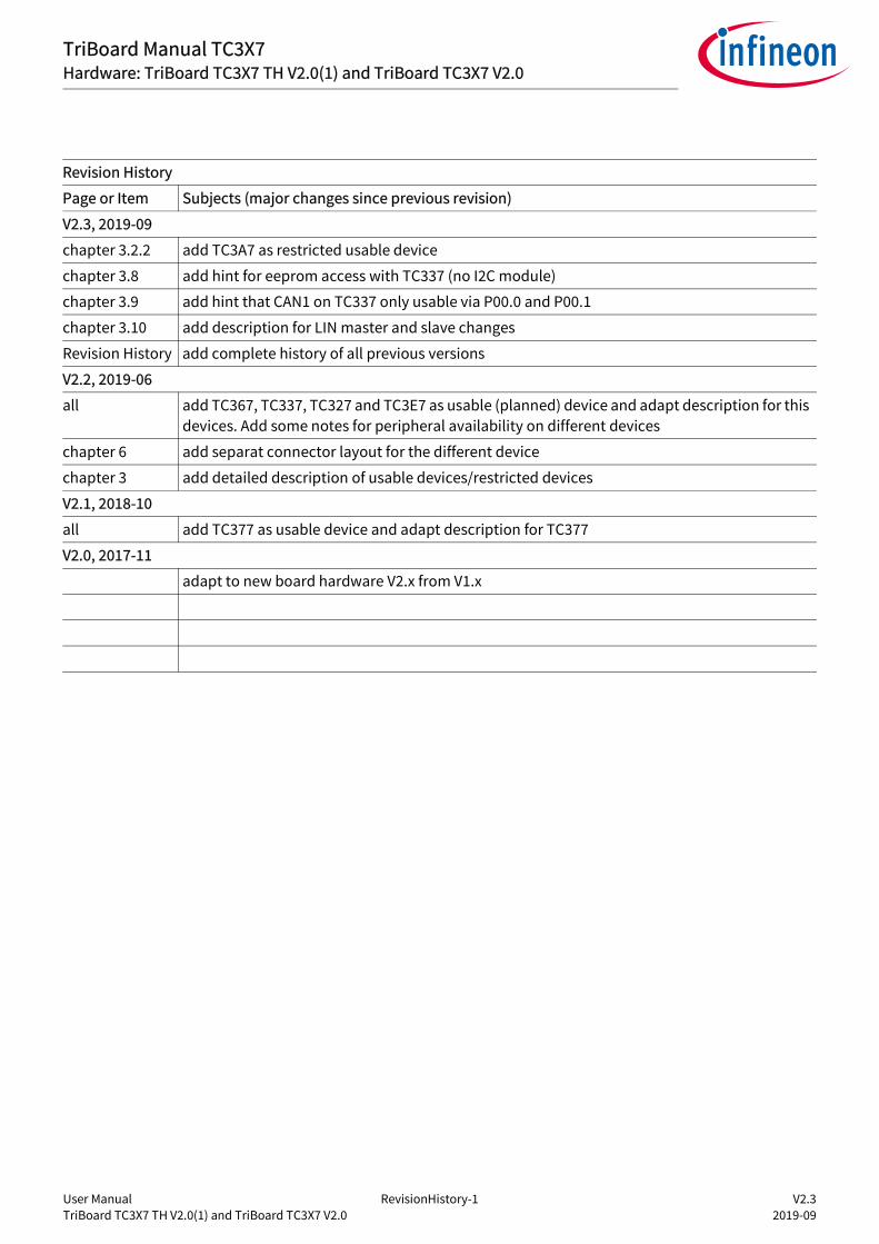
User Manual RevisionHistory-1 V2.3 TriBoard TC3X7 TH V2.0(1) and TriBoard TC3X7 V2.0 2019-09
TriBoard Manual TC3X7Hardware: TriBoard TC3X7 TH V2.0(1) and TriBoard TC3X7 V2.0
Revision History
Page or Item Subjects (major changes since previous revision)
V2.3, 2019-09
chapter 3.2.2 add TC3A7 as restricted usable device
chapter 3.8 add hint for eeprom access with TC337 (no I2C module)
chapter 3.9 add hint that CAN1 on TC337 only usable via P00.0 and P00.1
chapter 3.10 add description for LIN master and slave changes
Revision History add complete history of all previous versions
V2.2, 2019-06
all add TC367, TC337, TC327 and TC3E7 as usable (planned) device and adapt description for this devices. Add some notes for peripheral availability on different devices
chapter 6 add separat connector layout for the different device
chapter 3 add detailed description of usable devices/restricted devices
V2.1, 2018-10
all add TC377 as usable device and adapt description for TC377
V2.0, 2017-11
adapt to new board hardware V2.x from V1.x
Trademarks of Infineon Technologies AGµHVIC™, µIPM™, µPFC™, AU-ConvertIR™, AURIX™, C166™, CanPAK™, CIPOS™, CIPURSE™, CoolDP™, CoolGaN™, COOLiR™, CoolMOS™, CoolSET™, CoolSiC™,DAVE™, DI-POL™, DirectFET™, DrBlade™, EasyPIM™, EconoBRIDGE™, EconoDUAL™, EconoPACK™, EconoPIM™, EiceDRIVER™, eupec™, FCOS™, GaNpowIR™,HEXFET™, HITFET™, HybridPACK™, iMOTION™, IRAM™, ISOFACE™, IsoPACK™, LEDrivIR™, LITIX™, MIPAQ™, ModSTACK™, my-d™, NovalithIC™, OPTIGA™,OptiMOS™, ORIGA™, PowIRaudio™, PowIRStage™, PrimePACK™, PrimeSTACK™, PROFET™, PRO-SIL™, RASIC™, REAL3™, SmartLEWIS™, SOLID FLASH™,SPOC™, StrongIRFET™, SupIRBuck™, TEMPFET™, TRENCHSTOP™, TriCore™, UHVIC™, XHP™, XMC™.
Trademarks updated November 2015
Other TrademarksAll referenced product or service names and trademarks are the property of their respective owners.
Edition 2019-09Published by Infineon Technologies AG81726 Munich, Germany
© 2019 Infineon Technologies AG.All Rights Reserved.
Do you have a question about any aspect of this document?Email: [email protected]
Document referenceDoc_Number
IMPORTANT NOTICEThe information given in this document shall in noevent be regarded as a guarantee of conditions orcharacteristics ("Beschaffenheitsgarantie"). With respect to any examples, hints or any typicalvalues stated herein and/or any information regardingthe application of the product, Infineon Technologieshereby disclaims any and all warranties and liabilitiesof any kind, including without limitation warranties ofnon-infringement of intellectual property rights of anythird party. In addition, any information given in this document issubject to customer's compliance with its obligationsstated in this document and any applicable legalrequirements, norms and standards concerningcustomer's products and any use of the product ofInfineon Technologies in customer's applications. The data contained in this document is exclusivelyintended for technically trained staff. It is theresponsibility of customer's technical departments toevaluate the suitability of the product for the intendedapplication and the completeness of the productinformation given in this document with respect tosuch application.
For further information on technology, delivery termsand conditions and prices, please contact the nearestInfineon Technologies Office (www.infineon.com).
WARNINGS
Due to technical requirements products may containdangerous substances. For information on the typesin question please contact your nearest InfineonTechnologies office.
Except as otherwise explicitly approved by InfineonTechnologies in a written document signed byauthorized representatives of Infineon Technologies,Infineon Technologies’ products may not be used inany applications where a failure of the product or anyconsequences of the use thereof can reasonably beexpected to result in personal injury.
Please read the Important Notice and Warnings at the end of this document