TRF372017 Integrated IQ Modulator PLL/VCO datasheet (Rev. E)
61
R Div PFD Prescaler div p/p+1 Lock det Serial Interface CLK DATA LE REFIN CP_OUT VTUNE LO_OUT VCCs GNDs Div1/2/4/ 8 Pwr save PS From SPI S BBI BBQ RFOUT Div2/ 4/8 Poly- Phase SD control From SPI Vcm D/A From SPI Vcm D/A From SPI Charge Pump EXT_VCO RF Divider N- Divider From SPI LD Product Folder Sample & Buy Technical Documents Tools & Software Support & Community TRF372017 SLWS224E – AUGUST 2010 – REVISED JANUARY 2016 TRF372017 Integrated IQ Modulator PLL/VCO 1 Features 3 Description TRF372017 is a high-performance, direct up- 1• Fully Integrated PLL/VCO and IQ Modulator conversion device, integrating a high-linearity, low- • LO Frequency from 300 MHz to 4.8 GHz noise IQ modulator and an integer-fractional • 76-dBc Single-Carrier WCDMA ACPR at –8-dBm PLL/VCO. The VCO uses integrated frequency Channel Power dividers to achieve a wide, continuous tuning range of 300 MHz to 4800 MHz. The LO is available as an • OIP3 of 26 dBm output with independent frequency dividers. The • P1dB of 11.5 dBm device also accepts input from an external LO or • Integer/Fractional PLL VCO. The modulator baseband inputs can be biased either internally or externally. Internal DC offset • Phase Noise –132 dBc/Hz adjustment enables carrier cancellation. The device is (at 1 MHz, f VCO of 2.3 GHz) controlled through a 3-wire serial programming • Low Noise Floor: –160 dBm/Hz interface (SPI). A control pin invokes power-save • Input Reference Frequency Range: Up to mode to reduce power consumption while keeping 160 MHz the VCO locked for fast start-up. • VCO Frequency Divided by 1-2-4-8 Output Device Information (1) PART NUMBER PACKAGE BODY SIZE (NOM) 2 Applications TRF372017 VQFN (48) 7.00 mm × 7.00 mm • Wireless Infrastructure (1) For all available packages, see the orderable addendum at – CDMA: IS95, UMTS, CDMA2000, TD-SCDMA the end of the data sheet. – TDMA: GSM, IS-136, EDGE/UWC-136 – LTE • Wireless Local Loop • Point-to-Point Wireless Access • Wireless MAN Wideband Transceivers spacing Block Diagram 1 An IMPORTANT NOTICE at the end of this data sheet addresses availability, warranty, changes, use in safety-critical applications, intellectual property matters and other important disclaimers. PRODUCTION DATA.
Transcript of TRF372017 Integrated IQ Modulator PLL/VCO datasheet (Rev. E)

RD
iv
PFD
Pre
sca
ler
div
p/p
+1
Lo
ck
det
Serial
Inte
rfa
ce
CLK
DATA
LE
RE
FIN
CP_OUT
VT
UN
E
LO
_O
UT
VC
Cs
GN
Ds
Div
1/2
/4/
8
Pw
r
sa
ve
PS
From
SPI
S
BBI
BBQ
RFOUTDiv2/
4/8
Poly-
Phase
SD
contr
ol
Fro
m
SP
I
Vcm
D/A
From
SPI
Vcm
D/A
From
SPI
Charge
Pump
EX
T_V
CO
RF
Div
ider
N-
Div
ide
r
From
SPI
LD
Product
Folder
Sample &Buy
Technical
Documents
Tools &
Software
Support &Community
TRF372017SLWS224E –AUGUST 2010–REVISED JANUARY 2016
TRF372017 Integrated IQ Modulator PLL/VCO1 Features 3 Description
TRF372017 is a high-performance, direct up-1• Fully Integrated PLL/VCO and IQ Modulator
conversion device, integrating a high-linearity, low-• LO Frequency from 300 MHz to 4.8 GHz noise IQ modulator and an integer-fractional• 76-dBc Single-Carrier WCDMA ACPR at –8-dBm PLL/VCO. The VCO uses integrated frequency
Channel Power dividers to achieve a wide, continuous tuning range of300 MHz to 4800 MHz. The LO is available as an• OIP3 of 26 dBmoutput with independent frequency dividers. The• P1dB of 11.5 dBm device also accepts input from an external LO or
• Integer/Fractional PLL VCO. The modulator baseband inputs can be biasedeither internally or externally. Internal DC offset• Phase Noise –132 dBc/Hzadjustment enables carrier cancellation. The device is(at 1 MHz, fVCO of 2.3 GHz)controlled through a 3-wire serial programming• Low Noise Floor: –160 dBm/Hz interface (SPI). A control pin invokes power-save
• Input Reference Frequency Range: Up to mode to reduce power consumption while keeping160 MHz the VCO locked for fast start-up.
• VCO Frequency Divided by 1-2-4-8 OutputDevice Information(1)
PART NUMBER PACKAGE BODY SIZE (NOM)2 ApplicationsTRF372017 VQFN (48) 7.00 mm × 7.00 mm• Wireless Infrastructure(1) For all available packages, see the orderable addendum at– CDMA: IS95, UMTS, CDMA2000, TD-SCDMA the end of the data sheet.
– TDMA: GSM, IS-136, EDGE/UWC-136– LTE
• Wireless Local Loop• Point-to-Point Wireless Access• Wireless MAN Wideband Transceivers
spacing
Block Diagram
1
An IMPORTANT NOTICE at the end of this data sheet addresses availability, warranty, changes, use in safety-critical applications,intellectual property matters and other important disclaimers. PRODUCTION DATA.

TRF372017SLWS224E –AUGUST 2010–REVISED JANUARY 2016 www.ti.com
Table of Contents7.4 Device Functional Modes........................................ 331 Features .................................................................. 17.5 Register Maps ......................................................... 342 Applications ........................................................... 1
8 Application and Implementation ........................ 463 Description ............................................................. 18.1 Application Information............................................ 464 Revision History..................................................... 28.2 Typical Application ................................................. 465 Pin Configuration and Functions ......................... 3
9 Power Supply Recommendations ...................... 506 Specifications......................................................... 510 Layout................................................................... 516.1 Absolute Maximum Ratings ...................................... 5
10.1 Layout Guidelines ................................................. 516.2 Recommended Operating Conditions....................... 510.2 Layout Example .................................................... 516.3 Thermal Information .................................................. 5
11 Device and Documentation Support ................. 526.4 Electrical Characteristics........................................... 611.1 Device Support...................................................... 526.5 Timing Requirements - SPI: Writing Phase .............. 811.2 Community Resources.......................................... 526.6 Timing Requirements - SPI: Read-Back Phase........ 811.3 Trademarks ........................................................... 526.7 Typical Characteristics ............................................ 1011.4 Electrostatic Discharge Caution............................ 527 Detailed Description ............................................ 2311.5 Glossary ................................................................ 527.1 Overview ................................................................. 23
12 Mechanical, Packaging, and Orderable7.2 Functional Block Diagram ....................................... 23Information ........................................................... 527.3 Feature Description................................................. 23
4 Revision HistoryNOTE: Page numbers for previous revisions may differ from page numbers in the current version.
Changes from Revision D (September 2013) to Revision E Page
• Added Feature Description section, Device Functional Modes section, Application and Implementation section,Power Supply Recommendations section, Layout section, Device and Documentation Support section, andMechanical, Packaging, and Orderable Information section .................................................................................................. 1
Changes from Revision C (May 2012) to Revision D Page
• Changed text string from Reg 1, B[30..28] = [000] to Reg 0, B[30..28] = [000] in the Description column associatedwith RB_REG<0>, RB_REG<1>, and RB_REG<2> ............................................................................................................ 44
Changes from Revision B (March 2012) to Revision C Page
• Added graph titles to Figure 56 and 57 that were missing in Revision B............................................................................. 17
Changes from Revision A (August 2010) to Revision B Page
• Deleted Comments column from Table 1............................................................................................................................... 8• Changed Figures 12 through Figure 27 ............................................................................................................................... 10• Changed the text under Integer and Fractional Mode Selection through Practical Limit on Maximum PFD Frequency. .... 23• Changed RDIV = 20 to RDIV = 2 in Setup Example for Fractional Mode............................................................................ 26• Changed Recommended Value of EN_LD_ISOURCE from 1 to 0 in Table 1..................................................................... 27• Changed column heading from Default Value to Reset Value in register tables 1, 2, 3, 4, 5, 6, and 7............................... 34• Added recommended programming [xx] to various Description statements in register tables 2, 5, 6, and 7. ..................... 37• Changed Register 4, Bit21/Bit22 Description statement from Off to Normal. ...................................................................... 39• Changed Column heading from Default Value to Reset Value in Readback mode section, Register 0.............................. 43• Changed Bit5 name from CHIP_ID to CHIP_ID _0 and changed Bit6 name from NU to CHIP_ID_1, Reset Value to 1.... 44• Changed image in Figure 87. .............................................................................................................................................. 48• Changed the text in the Application Layout, and added link to Figure 95............................................................................ 51
2 Submit Documentation Feedback Copyright © 2010–2016, Texas Instruments Incorporated

VCC_LO1
13
14
15
16
17
1
2
3
4
5
44
45
46
47
48
36
35
34
33
32
6
7
8
9
101
8
19
20
21
22
31
30
29
28
27
39
40
41
42
43
VCC_DIG
GND_DIG
GND
LD
BBQ_N
BBQ_P
GND
RS
VD
GN
D
RF
OU
T
VC
C_M
IX
GN
D
LO_OUT_P
LO_OUT_N
CLK
DA
TA
LE
EXT_VCO
BBI_N
BBI_P
GND
RE
FIN
GN
D
VC
C_P
LL
CP
_O
UT
GN
D
GN
D
VT
UN
E
VCC_VCO2
GN
D
VCC_LO2
GND
GN
D
VC
C_
D2S
GN
D
GN
D
GND 11
12
23
24
26
25
37
38
PS
RDBK
GND
GN
D
GN
D
GN
D
GND
GND
VCC_VCO1
SC
AN
_E
N
TRF372017www.ti.com SLWS224E –AUGUST 2010–REVISED JANUARY 2016
5 Pin Configuration and Functions
RGZ Package48-Pin VQFN
Top View
Pin FunctionsPIN
I/O DESCRIPTIONNAME NO.
Base-band in-phase input: positive terminal. Internal 5 kΩ to VCM generator. If VCM isBBI_P 27 I internally generated (PWD_BB_VCM = 0), external AC coupling caps and 100-Ω differential
termination to BBI_N is required.Base-band in-phase input: negative terminal. Internal 5 kΩ to VCM generator. If VCM is
BBI_N 28 I internally generated (PWD_BB_VCM = 0), external AC coupling caps and 100-Ω differentialtermination to BBI_P is required.Base-band in-quadrature input: negative terminal. Internal 5 kΩ to VCM generator. If VCM is
BBQ_N 9 I internally generated (PWD_BB_VCM = 0), external AC coupling caps and 100-Ω differentialtermination to BBQ_P is required.Base-band in-quadrature input: positive terminal. Internal 5 kΩ to VCM generator. If VCM is
BBQ_P 10 I internally generated (PWD_BB_VCM = 0), external AC coupling caps and 100-Ω differentialtermination to BBQ_N is required.
CLK 47 I SPI clock input. Digital input. High impedance.CP_OUT 40 O Charge pump outputDATA 46 I SPI data input. Digital input. High impedance.EXT_VCO 36 I External local oscillator input. High impedance. Normally AC-coupled.
6, 8, 11, 12, 13,15, 16, 17, 19,
GND 22, 23, 24, 25, — Ground26, 29, 31, 37,
39, 42, 44GND_DIG 4 — Digital ground
PLL lock detect output, as configured by MUX_CTRL. Digital output pins can source or sinkLD 5 O up to 8 mA of current.LE 45 I SPI latch enable. Digital input. High impedance.
Copyright © 2010–2016, Texas Instruments Incorporated Submit Documentation Feedback 3
TRF372017SLWS224E –AUGUST 2010–REVISED JANUARY 2016 www.ti.com
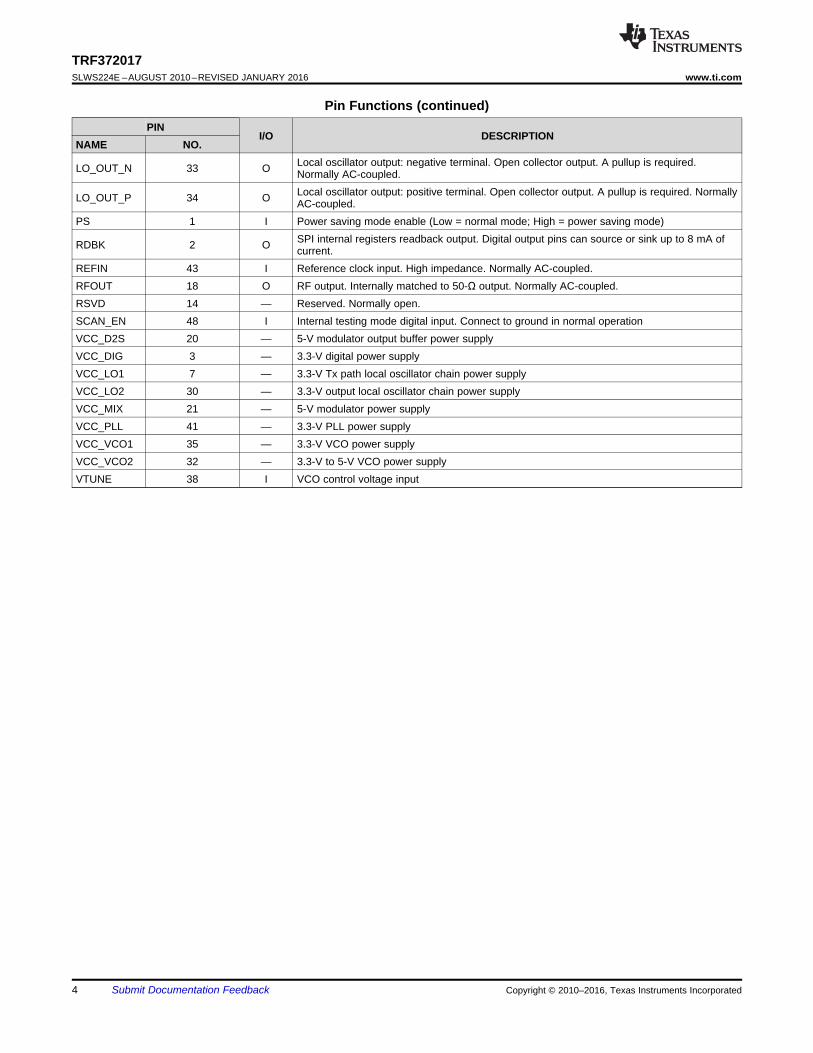
Pin Functions (continued)PIN
I/O DESCRIPTIONNAME NO.
Local oscillator output: negative terminal. Open collector output. A pullup is required.LO_OUT_N 33 O Normally AC-coupled.Local oscillator output: positive terminal. Open collector output. A pullup is required. NormallyLO_OUT_P 34 O AC-coupled.
PS 1 I Power saving mode enable (Low = normal mode; High = power saving mode)SPI internal registers readback output. Digital output pins can source or sink up to 8 mA ofRDBK 2 O current.
REFIN 43 I Reference clock input. High impedance. Normally AC-coupled.RFOUT 18 O RF output. Internally matched to 50-Ω output. Normally AC-coupled.RSVD 14 — Reserved. Normally open.SCAN_EN 48 I Internal testing mode digital input. Connect to ground in normal operationVCC_D2S 20 — 5-V modulator output buffer power supplyVCC_DIG 3 — 3.3-V digital power supplyVCC_LO1 7 — 3.3-V Tx path local oscillator chain power supplyVCC_LO2 30 — 3.3-V output local oscillator chain power supplyVCC_MIX 21 — 5-V modulator power supplyVCC_PLL 41 — 3.3-V PLL power supplyVCC_VCO1 35 — 3.3-V VCO power supplyVCC_VCO2 32 — 3.3-V to 5-V VCO power supplyVTUNE 38 I VCO control voltage input
4 Submit Documentation Feedback Copyright © 2010–2016, Texas Instruments Incorporated

TRF372017www.ti.com SLWS224E –AUGUST 2010–REVISED JANUARY 2016
6 Specifications
6.1 Absolute Maximum Ratingsover operating free-air temperature range (unless otherwise noted) (1) (2)
MIN MAX UNITSupply voltage (3) –0.3 5.5 VDigital I/O voltage –0.3 VCC + 0.5 V
TJ Operating virtual junction temperature –40 150 °CTA Operating ambient temperature –40 85 °CTstg Storage temperature –40 150 °C
(1) Stresses beyond those listed under Absolute Maximum Ratings may cause permanent damage to the device. These are stress ratingsonly, which do not imply functional operation of the device at these or any other conditions beyond those indicated under RecommendedOperating Conditions. Exposure to absolute-maximum-rated conditions for extended periods may affect device reliability.
(2) ESD rating not valid for RF sensitive pins.(3) All voltage values are with respect to network ground terminal.
6.2 Recommended Operating ConditionsMIN NOM MAX UNIT
VCC5V 5-V power supply voltage 4.5 5 5.5 VVCC3V 3.3-V power supply voltage 3 3.3 3.6 VVCC_VCO2 3.3-V to 5-V power supply voltage 3 3.3 5.5 VTA Operating ambient temperature –40 85 °CTJ Operating virtual junction temperature –40 125 °C
6.3 Thermal InformationTRF372017
THERMAL METRIC (1) RGZ (VQFN) UNIT48 PINS
RθJA Junction-to-ambient thermal resistance 30.0 °C/WRθJC(top) Junction-to-case (top) thermal resistance 10.0 °C/WRθJB Junction-to-board thermal resistance 8.0 °C/WψJT Junction-to-top characterization parameter 0.5 °C/WψJB Junction-to-board characterization parameter 7.0 °C/WRθJC(bot) Junction-to-case (bottom) thermal resistance 0.5 °C/W
(1) For more information about traditional and new thermal metrics, see the Semiconductor and IC Package Thermal Metrics applicationreport, SPRA953.
Copyright © 2010–2016, Texas Instruments Incorporated Submit Documentation Feedback 5

TRF372017SLWS224E –AUGUST 2010–REVISED JANUARY 2016 www.ti.com
6.4 Electrical CharacteristicsVCC5V = 5 V, VCC3V = 3.3 V, VCC_VCO2 = 3.3 V, TA = 25°C, internal LO, internal VCM (unless otherwise noted)
PARAMETER TEST CONDITIONS MIN TYP MAX UNIT
DC PARAMETERS
3.3-V power supply, LO on 200 250 mAICC Total supply current, LO on (1)
5-V power supply, LO on 117 148 mA
VCC_DIG, LO on 3 5 mA
VCC_LO1 and VCC_LO2 121 130 mA
VCC_D2S 43 60 mA
VCC_MIX 74 90 mASupply current, LO on (1)
VCC_VCO1 20 28mA
VCC_VCO2 17 20
LO_OUT_N and LO_OUT_P 17 28 mA
VCC_PLL 24 40 mA
3.3-V power supply, LO off 165 204 mATotal supply current, LO off (1)
5-V power supply, LO off 117 149 mA
3.3-V power supply, PS on 65 94 mATotal supply current, PS on (1)
5-V power supply, PS on 51 73 mA
BASEBAND INPUTS
Externally generated 1.7 VVcm I and Q input DC common voltage (2)
Set internally 1.6 1.7 1.85 V
BW 1-dB input frequency bandwidth 1000 MHz
Resistance 5 kΩZI Input Impedance
Parallel Capacitance 3 pF
BASEBAND INPUT DC OFFSET CONTROL D/A (3)
Number of bits Programmed through SPI 8
|BBI_P - BBI_N| or |BBQ_P - BBQ_N|, 100-ΩProgrammable DC offset setting 0.02 Vdifferential load
DIGITAL INTERFACE
VIH High-level input voltage 2 3.3 V
VIL Low-level input voltage 0 0.8 V
VOH High-level output voltage Referenced to VCC_DIG 0.8 × Vcc V
VOL Low-level output voltage Referenced to VCC_DIG 0.2 × Vcc V
REFERENCE OSCILLATOR PARAMETERS
Fref Reference frequency 160 MHz
Reference input sensitivity 0.2 3.3 Vp-p
Parallel capacitance 5 pFReference input impedance
Parallel resistance 3900 Ω
PFD CHARGE PUMP
PFD frequency (4) 100 MHz
ICP Charge pump current SPI programmable 1.94 mA
IQ MODULATOR OUTPUT, FLO = 750 MHz
Output RMS voltage over se input I (or Q) RMSG Voltage gain –4 –3.2 –2.4 dBvoltage
P1dB Output compression point 11 dBm
IP3 Output IP3 2 input tones at 4.5 and 5.5 MHz 26 dBm
IP2 Output IP2 2 input tones at 4.5 and 5.5 MHz 56.5 dBm
Carrier feedthrough Unadjusted –43.5 dBm
Sideband suppression Unadjusted –46 dBc
Output return loss 10 dB
(1) Maximum current is worst-case overvoltage, temperature, and expected process variations.(2) The TRF372017 can generate the input common voltage internally or can accept an external common mode voltage. The two modes
are selectable through SPI.(3) When the internal input common mode voltage is selected, it is possible to apply some DC offset with the integrated D/A.(4) See Application Information for discussion on selection of PFD frequency.
6 Submit Documentation Feedback Copyright © 2010–2016, Texas Instruments Incorporated

TRF372017www.ti.com SLWS224E –AUGUST 2010–REVISED JANUARY 2016
Electrical Characteristics (continued)VCC5V = 5 V, VCC3V = 3.3 V, VCC_VCO2 = 3.3 V, TA = 25°C, internal LO, internal VCM (unless otherwise noted)
PARAMETER TEST CONDITIONS MIN TYP MAX UNIT
DC only to BB inputs; 13-MHz offset from LO; PoutOutput noise –162 dBm/Hz= –10 dBm
IQ MODULATOR OUTPUT, FLO = 900 MHz
Output RMS voltage over se input I (or Q) RMSG Voltage gain –4 –3.4 –2.4 dBvoltage
P1dB Output compression point 11 dBm
IP3 Output IP3 2 input tones at 4.5 and 5.5 MHz 26.5 dBm
IP2 Output IP2 2 input tones at 4.5 and 5.5 MHz 56.5 dBm
Carrier feedthrough Unadjusted –43 dBm
Sideband suppression Unadjusted –45 dBc
Output return loss 10 dB
DC only to BB inputs; 13-MHz offset from LO; PoutOutput noise –160 dBm/Hz= –10 dBm
IQ MODULATOR OUTPUT, FLO = 2150 MHz
Output RMS voltage over se input I (or Q) RMSG Voltage gain –4.2 –3.1 –2 dBvoltage
P1dB Output compression point 11.5 dBm
IP3 Output IP3 2 input tones at 4.5 and 5.5 MHz 25 dBm
IP2 Output IP2 2 input tones at 4.5 and 5.5 MHz 56 dBm
Carrier feedthrough Unadjusted –40 dBm
Sideband suppression Unadjusted –32 dBc
Output return loss 10 dB
DC only to BB inputs; 13-MHz offset from LO; PoutOutput noise –158 dBm/Hz= –10 dBm
1 WCDMA signal; Pout = –8 dBm –75ACPR Adjacent-channel power ratio dBc
2 WCDMA signals; Pout = –11 dBm per carrier 71
IQ MODULATOR OUTPUT, FLO = 2700 MHz
Output RMS voltage over se input I (or Q) RMSG Voltage gain –4.1 –2.7 –1.3 dBvoltage
P1dB Output compression point 12 dBm
IP3 Output IP3 2 input tones at 4.5 and 5.5 MHz 26.5 dBm
IP2 Output IP2 2 input tones at 4.5 and 5.5 MHz 50 dBm
Carrier feedthrough Unadjusted –43 dBm
Sideband suppression Unadjusted –41 dBc
Output return loss 10 dB
DC only to BB inputs; 13-MHz offset from LO; PoutOutput noise –153 dBm/Hz= –10 dBm
LOCAL OSCILLATOR
VCO range 2400 4800
Divide by 2 1200 2400FVCO Frequency range MHz
Divide by 4 600 1200
Divide by 8 300 600
Free running VCO 10 kHz –85 dBc/Hz
Phase noise, Fout = 2.3 GHz 1 MHz –132 dBc/Hz
10 MHz –150 dBc/Hz
50 MHz –153 dBc/Hz
PLO LO output power (5) 100-Ω differential, external load; single-ended –2.5 3 dBm
(5) With VCO frequency at 4.6 GHz and LO in divide-by-2 mode at 2.3 GHz
Copyright © 2010–2016, Texas Instruments Incorporated Submit Documentation Feedback 7

1st
Write
clock
pulse
32nd
Write
clock
pulse
tw
CLOCK
DATA
LATCHENABLE
RE
GIS
TE
RW
RIT
E
DB1
Address Bit1DB2
Address Bit2
DB3
Address Bit3DB29 DB30
DB0 (LSB)
Address Bit0
tsu3
tsu1 th t(CLK)
DB31 (MSB)
t(CL)
t(CH)
tsu2
End of WriteCycle pulse
TRF372017SLWS224E –AUGUST 2010–REVISED JANUARY 2016 www.ti.com
6.5 Timing Requirements - SPI: Writing Phase (1)
MIN TYP MAX UNITth Hold time, data to clock 20 nstSU1 Setup time, data to clock 20 nsT(CH) Clock low duration 20 nsT(CL) Clock high duration 20 nstSU2 Setup time, clock to enable 20 nst(CLK) Clock period 50 nstW Enable time 50 nstSU3 Setup time, latch to data 70 ns
(1) See Figure 1 for timing diagram.
6.6 Timing Requirements - SPI: Read-Back Phase (1)
MIN TYP MAX UNITth Hold time, data to clock 20 nstSU1 Setup time, data to clock 20 nsT(CH) Clock low duration 20 nsT(CL) Clock High duration 20 nstSU2 Setup time, clock to enable 20 nstd Delay time, clock to readback data output 10 nstW Enable time (2) 50 nst(CLK) Clock period 50 ns
(1) See Figure 2 for timing diagram.(2) Equals Clock period
Figure 1. SPI Write Timing Diagram
8 Submit Documentation Feedback Copyright © 2010–2016, Texas Instruments Incorporated

32nd
Writeclockpulse
1st Readclock pulse
2nd
Readclock pulse
32nd
Readclock pulse
33rd
Readclock pulse
“End of Write Cycle”pulse
ReadBackData Bit31
ReadBackDataBit1
ReadBackDataBit29
ReadBackData Bit30
ReadBackData Bit 0
DB31(MSB)
1st
Writeclockpulse
tsu1 th t(CLK)
32nd Writeclock pulse
DB30DB29DB2
Address Bit 2DB1
Address Bit1
DB0 (LSB)
Address Bit 0
CLOCK
DATA
CLOCK
READBACK DATA
RE
GIS
TE
RW
RIT
ER
EA
DB
AC
K
td
tsu2
twLATCH ENABLE
T(CL)
T(CH)
tsu3
LATCH ENABLE
DB3Address Bit 3
TRF372017www.ti.com SLWS224E –AUGUST 2010–REVISED JANUARY 2016
Figure 2. SPI Read-Back Timing Diagram
Copyright © 2010–2016, Texas Instruments Incorporated Submit Documentation Feedback 9

Frequency (Hz)
Phase
Nois
e(d
Bc/H
z)
-160
-140
-120
-100
-80
-60
-40
1k 10k 100k 1M 10M 40M
VCC = 3 V
VCC = 3.3 V
VCC = 3.6 V
G005
F_LO_OUT = 2.6 GHzTA = 25°C
Frequency (Hz)
Phase
Nois
e(d
Bc/H
z)
-160
-140
-120
-100
-80
-60
-40
1k 10k 100k 1M 10M 40M
VCC = 3 V
VCC = 3.3 V
VCC = 3.6 V
G006
F_LO_OUT = 3.35 GHzTA = 25°C
Frequency (Hz)
Phase
Nois
e(d
Bc/H
z)
-160
-140
-120
-100
-80
-60
-40
1k 10k 100k 1M 10M 40M
TA = -40°C
TA = 25°C
TA = 85°C
G003
F_LO_OUT = 4.05 GHzVCC = 3.3, 5 V
Frequency (Hz)
Phase
Nois
e(d
Bc/H
z)
-160
-140
-120
-100
-80
-60
-40
1k 10k 100k 1M 10M 40M
TA = -40°C
TA = 25°C
TA = 85°C
G004
F_LO_OUT = 4.7 GHzVCC = 3.3, 5 V
Frequency (Hz)
Phase
Nois
e(d
Bc/H
z)
-160
-140
-120
-100
-80
-60
-40
1k 10k 100k 1M 10M 40M
TA = -40°C
TA = 25°C
TA = 85°C
G001
F_LO_OUT = 2.6 GHzVCC = 3.3, 5 V
Frequency (Hz)
Phase
Nois
e(d
Bc/H
z)
-160
-140
-120
-100
-80
-60
-40
1k 10k 100k 1M 10M 40M
TA = -40°C
TA = 25°C
TA = 85°C
G002
F_LO_OUT = 3.35 GHzVCC = 3.3, 5 V
TRF372017SLWS224E –AUGUST 2010–REVISED JANUARY 2016 www.ti.com
6.7 Typical CharacteristicsVCM = 1.7 V (internal), VinBB = 300 mVrms single-ended sine wave in quadrature, VCC3V = 3.3 V, VCC5V = 5 V, fBB = 4.5 MHzand 5.5 MHz, internal LO, TA = 25°C; FPFD = 1.6 MHz (unless otherwise noted).
Figure 3. Open-Loop Phase Noise Figure 4. Open Loop Phase Noisevs Frequency and Temperature vs Frequency and Temperature
Figure 5. Open Loop Phase Noise Figure 6. Open Loop Phase Noisevs Frequency and Temperature vs Frequency and Temperature
Figure 7. Open Loop Phase Noise Figure 8. Open Loop Phase Noisevs Frequency and Supply Voltage vs Frequency and Supply Voltage
10 Submit Documentation Feedback Copyright © 2010–2016, Texas Instruments Incorporated

Frequency (Hz)
Ph
ase
No
ise
(d
Bc/H
z)
-160
-140
-120
-100
-80
-60
-40
1k 10k 100k 1M 10M 40M
TA = -40°C TA = 25°C
TA = 85°C
G011
F_LO_OUT = 650 MHzVCC = 3.3, 5 VDiv 4 Mode
Frequency (Hz)
Ph
ase
No
ise
(d
Bc/H
z)
-160
-140
-120
-100
-80
-60
-40
1k 10k 100k 1M 10M 40M
TA = -40°C
TA = 25°C
TA = 85°C
G012
F_LO_OUT = 325 MHzVCC = 3.3, 5 VDiv 8 Mode
Frequency (Hz)
Ph
ase
No
ise
(d
Bc/H
z)
-160
-140
-120
-100
-80
-60
-40
1k 10k 100k 1M 10M 40M
TA = -40°C
TA = 25°C
TA = 85°C
G009
F_LO_OUT = 2.6 GHzVCC = 3.3, 5 VDiv 1 Mode
Frequency (Hz)
Ph
ase
No
ise
(d
Bc/H
z)
-160
-140
-120
-100
-80
-60
-40
1k 10k 100k 1M 10M 40M
TA = -40°C
TA = 25°C
TA = 85°C
G010
F_LO_OUT = 1.3 GHzVCC = 3.3, 5 VDiv 2 Mode
Frequency (Hz)
Phase
Nois
e(d
Bc/H
z)
-160
-140
-120
-100
-80
-60
-40
1k 10k 100k 1M 10M 40M
VCC = 3 V
VCC = 3.3 V
VCC = 3.6 V
G007
F_LO_OUT = 4.05 GHzTA = 25°C
Frequency (Hz)
Phase
Nois
e(d
Bc/H
z)
-160
-140
-120
-100
-80
-60
-40
1k 10k 100k 1M 10M 40M
VCC = 3 V
VCC = 3.3 V
VCC = 3.6 V
G008
F_LO_OUT = 4.7 GHzTA = 25°C
TRF372017www.ti.com SLWS224E –AUGUST 2010–REVISED JANUARY 2016
Typical Characteristics (continued)VCM = 1.7 V (internal), VinBB = 300 mVrms single-ended sine wave in quadrature, VCC3V = 3.3 V, VCC5V = 5 V, fBB = 4.5 MHzand 5.5 MHz, internal LO, TA = 25°C; FPFD = 1.6 MHz (unless otherwise noted).
Figure 9. Open Loop Phase Noise Figure 10. Open Loop Phase Noisevs Frequency and Supply Voltage vs Frequency and Supply Voltage
Figure 11. Closed Loop Phase Noise Figure 12. Closed Loop Phase Noisevs Frequency and Temperature vs Frequency and Temperature
Figure 13. Closed Loop Phase Noise Figure 14. Closed Loop Phase Noisevs Frequency and Temperature vs Frequency and Temperature
Copyright © 2010–2016, Texas Instruments Incorporated Submit Documentation Feedback 11

Frequency (Hz)
Ph
ase
No
ise
(d
Bc/H
z)
-160
-140
-120
-100
-80
-60
-40
1k 10k 100k 1M 10M 40M
TA = -40°C
TA = 25°C
TA = 85°C
G017
F_LO_OUT = 4 GHzVCC = 3.3, 5 VDiv 1 Mode
Frequency (Hz)
Ph
ase
No
ise
(d
Bc/H
z)
-160
-140
-120
-100
-80
-60
-40
1k 10k 100k 1M 10M 40M
TA = -40°C
TA = 25°C
TA = 85°C
G018
F_LO_OUT = 2 GHzVCC = 3.3, 5 VDiv 2 Mode
Frequency (Hz)
Ph
ase
No
ise
(d
Bc/H
z)
-160
-140
-120
-100
-80
-60
-40
1k 10k 100k 1M 10M 40M
TA = -40°C
TA = 25°C
TA = 85°C
G015
F_LO_OUT = 850 MHzVCC = 3.3, 5 VDiv 4 Mode
Frequency (Hz)
Ph
ase
No
ise
(d
Bc/H
z)
-160
-140
-120
-100
-80
-60
-40
1k 10k 100k 1M 10M 40M
TA = -40°C
TA = 25°C
TA = 85°C
G016
F_LO_OUT = 425 MHzVCC = 3.3, 5 VDiv 8 Mode
Frequency (Hz)
Ph
ase
No
ise
(d
Bc/H
z)
-160
-140
-120
-100
-80
-60
-40
1k 10k 100k 1M 10M 40M
TA = -40°C
TA = 25°C
TA = 85°C
G013
F_LO_OUT = 3.4 GHzVCC = 3.3, 5 VDiv 1 Mode
Frequency (Hz)
Ph
ase
No
ise
(d
Bc/H
z)
-160
-140
-120
-100
-80
-60
-40
1k 10k 100k 1M 10M 40M
TA = -40°C
TA = 25°C
TA = 85°C
G014
F_LO_OUT = 1.7 GHzVCC = 3.3, 5 VDiv 2 Mode
TRF372017SLWS224E –AUGUST 2010–REVISED JANUARY 2016 www.ti.com
Typical Characteristics (continued)VCM = 1.7 V (internal), VinBB = 300 mVrms single-ended sine wave in quadrature, VCC3V = 3.3 V, VCC5V = 5 V, fBB = 4.5 MHzand 5.5 MHz, internal LO, TA = 25°C; FPFD = 1.6 MHz (unless otherwise noted).
Figure 15. Closed Loop Phase Noise Figure 16. Closed Loop Phase Noisevs Frequency and Temperature vs Frequency and Temperature
Figure 17. Closed Loop Phase Noise Figure 18. Closed Loop Phase Noisevs Frequency and Temperature vs Frequency and Temperature
Figure 19. Closed Loop Phase Noise Figure 20. Closed Loop Phase Noisevs Frequency and Temperature vs Frequency and Temperature
12 Submit Documentation Feedback Copyright © 2010–2016, Texas Instruments Incorporated

Frequency (Hz)
Phase N
ois
e (
dB
c/H
z)
-160
-140
-120
-100
-80
-60
-40
1k 10k 100k 1M 10M 40M
TA = -40°CTA = 25°C
TA = 85°C
G023
F_LO_OUT = 1.15 GHzVCC = 3.3, 5 VDiv 4 Mode
Frequency (Hz)
Phase N
ois
e (
dB
c/H
z)
-160
-140
-120
-100
-80
-60
-40
1k 10k 100k 1M 10M 40M
TA = -40°CTA = 25°C
TA = 85°C
G024
F_LO_OUT = 575 MHzVCC = 3.3, 5 VDiv 8 Mode
Frequency (Hz)
Phase N
ois
e (
dB
c/H
z)
-160
-140
-120
-100
-80
-60
-40
1k 10k 100k 1M 10M 40M
TA = -40°C
TA = 25°C
TA = 85°C
G021
F_LO_OUT = 4.6 GHzVCC = 3.3, 5 VDiv 1 Mode
Frequency (Hz)
Phase N
ois
e (
dB
c/H
z)
-160
-140
-120
-100
-80
-60
-40
1k 10k 100k 1M 10M 40M
TA = -40°C
TA = 25°C
TA = 85°C
G022
F_LO_OUT = 2.3 GHzVCC = 3.3, 5 VDiv 2 Mode
Frequency (Hz)
Ph
ase
No
ise
(d
Bc/H
z)
-160
-140
-120
-100
-80
-60
-40
1k 10k 100k 1M 10M 40M
TA = -40°CTA = 25°C
TA = 85°C
G019
F_LO_OUT = 1 GHzVCC = 3.3, 5 VDiv 4 Mode
Frequency (Hz)
Ph
ase
No
ise
(d
Bc/H
z)
-160
-140
-120
-100
-80
-60
-40
1k 10k 100k 1M 10M 40M
TA = -40°C
TA = 25°C
TA = 85°C
G020
F_LO_OUT = 500 MHzVCC = 3.3, 5 VDiv 8 Mode
TRF372017www.ti.com SLWS224E –AUGUST 2010–REVISED JANUARY 2016
Typical Characteristics (continued)VCM = 1.7 V (internal), VinBB = 300 mVrms single-ended sine wave in quadrature, VCC3V = 3.3 V, VCC5V = 5 V, fBB = 4.5 MHzand 5.5 MHz, internal LO, TA = 25°C; FPFD = 1.6 MHz (unless otherwise noted).
Figure 21. Closed Loop Phase Noise Figure 22. Closed Loop Phase Noisevs Frequency and Temperature vs Frequency and Temperature
Figure 23. Closed Loop Phase Noise Figure 24. Closed Loop Phase Noisevs Frequency and Temperature vs Frequency and Temperature
Figure 25. Closed Loop Phase Noise Figure 26. Closed Loop Phase Noisevs Frequency and Temperature vs Frequency and Temperature
Copyright © 2010–2016, Texas Instruments Incorporated Submit Documentation Feedback 13
Output Power (dBm)
Nois
eat13-M
Hz
Off
set (d
Bm
/Hz)
-15 -10 -5 0 5 10-180
-175
-170
-165
-160
-155
-150
-145
-140
-135
-130
f = 450 MHz
f = 750 MHz
f = 900 MHz
f = 2140 MHz
f = 2700 MHz
f = 3500 MHz
G029
VCC = 3.3, 5 VTA = 25°C
Frequency (MHz)
Voltage G
ain
(dB
)
300 800 1300 1800 2300 2800 3300 3800 4300 4800-7
-6
-5
-4
-3
-2
-1
0
1
2
TA = -40°C
TA = 25°C
TA = 85°C
G030
Frequency (MHz)
Nois
eat13-M
Hz
Off
set (d
Bm
/Hz)
350 700 1050 1400 1750 2100 2450 2800 3150 3500-190
-180
-170
-160
-150
-140
-130
TA = -40°C
TA = 25°C
TA = 85°C
G027
VCC = 3.3, 5 VExternal VCOPO = -10dBm
Frequency (MHz)
Nois
eat13-M
Hz
Off
set (d
Bm
/Hz)
350 700 1050 1400 1750 2100 2450 2800 3150 3500-190
-180
-170
-160
-150
-140
-130
VCC = 3 V
VCC = 3.3 V
VCC = 3.6 V
G028
TA = 25°CExternal VCOPO = -10dBm
Frequency (MHz)
Nois
eat13-M
Hz
Off
set (d
Bm
/Hz)
350 700 1050 1400 1750 2100 2450 2800 3150 3500-190
-180
-170
-160
-150
-140
-130
TA = -40°C
TA = 25°C
TA = 85°C
G025
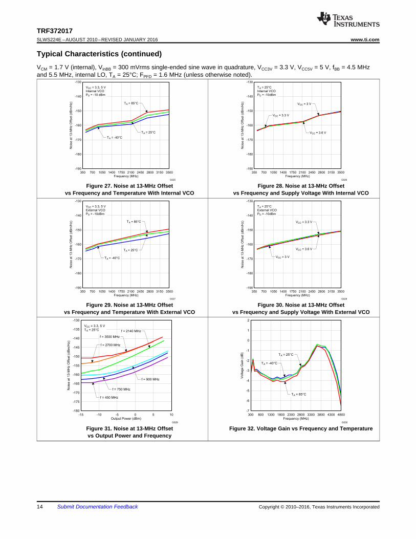
VCC = 3.3, 5 VInternal VCOPO = -10 dBm
Frequency (MHz)
Nois
eat13-M
Hz
Off
set (d
Bm
/Hz)
350 700 1050 1400 1750 2100 2450 2800 3150 3500-190
-180
-170
-160
-150
-140
-130
VCC = 3 V
VCC = 3.3 V
VCC = 3.6 V
G026
TA = 25°CInternal VCOPO = -10dBm
TRF372017SLWS224E –AUGUST 2010–REVISED JANUARY 2016 www.ti.com
Typical Characteristics (continued)VCM = 1.7 V (internal), VinBB = 300 mVrms single-ended sine wave in quadrature, VCC3V = 3.3 V, VCC5V = 5 V, fBB = 4.5 MHzand 5.5 MHz, internal LO, TA = 25°C; FPFD = 1.6 MHz (unless otherwise noted).
Figure 27. Noise at 13-MHz Offset Figure 28. Noise at 13-MHz Offsetvs Frequency and Temperature With Internal VCO vs Frequency and Supply Voltage With Internal VCO
Figure 29. Noise at 13-MHz Offset Figure 30. Noise at 13-MHz Offsetvs Frequency and Temperature With External VCO vs Frequency and Supply Voltage With External VCO
Figure 31. Noise at 13-MHz Offset Figure 32. Voltage Gain vs Frequency and Temperaturevs Output Power and Frequency
14 Submit Documentation Feedback Copyright © 2010–2016, Texas Instruments Incorporated

Frequency (MHz)
Voltage G
ain
(dB
)
2610 2620 2630 2640 2650 2660 2670 2680 2690-3.5
-3.4
-3.3
-3.2
-3.1
-3
-2.9
-2.8
-2.7
TA = -40°C
TA = 25°C
TA = 85°C
G035
Common-Mode Voltage (V)
Voltage G
ain
(dB
)
1.55 1.6 1.65 1.7 1.75 1.8 1.85 1.9-4.4
-4.2
-4
-3.8
-3.6
-3.4
-3.2
-3
-2.8
-2.6
-2.4
f = 750 MHz
f = 900 MHz
f = 1500 MHz
f = 2150 MHz
f = 2700 MHz
G036
Frequency (MHz)
Voltage G
ain
(dB
)
1465 1470 1475 1480 1485 1490 1495 1500 1505 1510-4.3
-4.2
-4.1
-4
-3.9
-3.8
-3.7
-3.6
TA = -40°C
TA = 25°C
TA = 85°C
G033
Frequency (MHz)
Voltage G
ain
(dB
)
2100 2110 2120 2130 2140 2150 2160 2170-4.4
-4.3
-4.2
-4.1
-4
-3.9
-3.8
-3.7
-3.6
-3.5
-3.4
TA = -40°C
TA = 25°C
TA = 85°C
G034
Frequency (MHz)
Voltage G
ain
(dB
)
720 725 730 735 740 745 750 755 760 765 770-3.5
-3.4
-3.3
-3.2
-3.1
-3
TA = -40°C
TA = 25°C
TA = 85°C
G031
Frequency (MHz)
Voltage G
ain
(dB
)
880 885 890 895 900 905 910 915 920-3.6
-3.55
-3.5
-3.45
-3.4
-3.35
-3.3
-3.25
-3.2
TA = -40°C
TA = 25°C
TA = 85°C
G032
TRF372017www.ti.com SLWS224E –AUGUST 2010–REVISED JANUARY 2016
Typical Characteristics (continued)VCM = 1.7 V (internal), VinBB = 300 mVrms single-ended sine wave in quadrature, VCC3V = 3.3 V, VCC5V = 5 V, fBB = 4.5 MHzand 5.5 MHz, internal LO, TA = 25°C; FPFD = 1.6 MHz (unless otherwise noted).
Figure 33. Voltage Gain Figure 34. Voltage Gainvs Frequency and Temperature at 750 MHz vs Frequency and Temperature at 900 MHz
Figure 35. Voltage Gain Figure 36. Voltage Gainvs Frequency and Temperature at 1500 MHz vs Frequency and Temperature at 2150 MHz
Figure 37. Voltage Gain Figure 38. Voltage Gainvs Frequency and Temperature at 2650 MHz vs Common-Mode Voltage and Frequency
Copyright © 2010–2016, Texas Instruments Incorporated Submit Documentation Feedback 15

Frequency (MHz)
P1dB
(dB
m)
850 860 870 880 890 900 910 920 930 940 95010.5
10.6
10.7
10.8
10.9
11
11.1
11.2
11.3
11.4
TA = -40°C
TA = 25°C
TA = 85°C
G041
Frequency (MHz)
P1dB
(dB
m)
1450 1460 1470 1480 1490 1500 1510 1520 1530 1540 155010.5
10.6
10.7
10.8
10.9
11
11.1
11.2
11.3
11.4
11.5
TA = -40°C
TA = 25°C
TA = 85°C
G042
Frequency (MHz)
P1dB
(dB
m)
300 800 1300 1800 2300 2800 3300 3800 4300 48005
6
7
8
9
10
11
12
13
14
15
TA = -40°C
TA = 25°C
TA = 85°C
G039
Frequency (MHz)
P1dB
(dB
m)
700 710 720 730 740 750 760 770 780 790 80010.5
10.6
10.7
10.8
10.9
11
11.1
11.2
11.3
TA = -40°C
TA = 25°C
TA = 85°C
G040
Baseband Voltage Amplitude (mV)
Voltage G
ain
(dB
)
0 100 200 300 400 500 600 700 800 900 1000-4.5
-4.3
-4.1
-3.9
-3.7
-3.5
-3.3
-3.1
-2.9
-2.7
-2.5
f = 750 MHz
f = 900 MHz
f = 1500 MHz
f = 2150 MHz
f = 2700 MHz
G037
BB Voltage is Single-Ended RMS
Frequency (MHz)
Voltage G
ain
(dB
)
300 800 1300 1800 2300 2800 3300 3800 4300 4800-5
-4
-3
-2
-1
0
1
VCC = 3 V
VCC = 3.3 V
VCC = 3.6 V
G038
TRF372017SLWS224E –AUGUST 2010–REVISED JANUARY 2016 www.ti.com
Typical Characteristics (continued)VCM = 1.7 V (internal), VinBB = 300 mVrms single-ended sine wave in quadrature, VCC3V = 3.3 V, VCC5V = 5 V, fBB = 4.5 MHzand 5.5 MHz, internal LO, TA = 25°C; FPFD = 1.6 MHz (unless otherwise noted).
Figure 39. Voltage Gain Figure 40. Voltage Gain vs Frequency and Supply Voltagevs Baseband Voltage Amplitude and Frequency
Figure 41. P1dB vs Frequency and Temperature Figure 42. P1dB vs Frequency and Temperature at 750 MHz
Figure 43. P1dB vs Frequency and Temperature at 900 MHz Figure 44. P1dB vs Frequency and Temperature at 1500 MHz
16 Submit Documentation Feedback Copyright © 2010–2016, Texas Instruments Incorporated

Frequency (MHz)
OIP
3 (
dB
m)
300 800 1300 1800 2300 2800 3300 3800 4300 480014
16
18
20
22
24
26
28
30
32
34
TA = -40°C
TA = 25°C
TA = 85°C
G047
Frequency (MHz)
OIP
3 (
dB
m)
880 885 890 895 900 905 910 915 92024
24.5
25
25.5
26
26.5
27
27.5
28
TA = -40°C
TA = 25°CTA = 85°C
G048
Common-Mode Voltage (V)
P1dB
(dB
m)
1.55 1.6 1.65 1.7 1.75 1.8 1.85 1.98
9
10
11
12
13
14
f = 750 MHz
f = 900 MHz
f = 1500 MHz
f = 2150 MHz
f = 2700 MHz
G045
Frequency (MHz)
P1dB
(dB
m)
300 800 1300 1800 2300 2800 3300 3800 4300 48006
7
8
9
10
11
12
13
14
15
VCC = 3 V
VCC = 3.3 V
VCC = 3.6 V
G046
Frequency (MHz)
P1dB
(dB
m)
2100 2110 2120 2130 2140 2150 2160 2170 2180 2190 220010.8
11
11.2
11.4
11.6
11.8
12
12.2
TA = -40°C
TA = 25°C
TA = 85°C
G043
Frequency (MHz)
P1dB
(dB
m)
2650 2660 2670 2680 2690 2700 2710 2720 2730 2740 275011
11.2
11.4
11.6
11.8
12
12.2
12.4
12.6
TA = -40°C
TA = 25°C
TA = 85°C
G044
TRF372017www.ti.com SLWS224E –AUGUST 2010–REVISED JANUARY 2016
Typical Characteristics (continued)VCM = 1.7 V (internal), VinBB = 300 mVrms single-ended sine wave in quadrature, VCC3V = 3.3 V, VCC5V = 5 V, fBB = 4.5 MHzand 5.5 MHz, internal LO, TA = 25°C; FPFD = 1.6 MHz (unless otherwise noted).
Figure 45. P1dB vs Frequency and Temperature at 2150 MHz Figure 46. P1dB vs Frequency and Temperature at 2700 MHz
Figure 47. P1dB vs Common-Mode Voltage and Frequency Figure 48. P1dB vs Frequency and Supply Voltage
Figure 49. OIP3 vs Frequency and Temperature Figure 50. OIP3 vs Temperature and Frequency at 900 MHz
Copyright © 2010–2016, Texas Instruments Incorporated Submit Documentation Feedback 17

OIP
3 (
dB
m)
1.5 1.55 1.6 1.65 1.7 1.75 1.8 1.85 1.9Common-Mode Voltage (V)
G053
29
28
27
26
25
24
23
22
21
TA
= 25 C°
f = 750 MHz
f = 1500 MHz
f = 2150 MHz
f = 900 MHz
f = 2700 MHz
f = 2150 MHzf = 900 MHz
f = 750 MHz
f = 2700 MHz
f = 1500 MHz
BB Voltage is Single-Ended RMS
30
29
28
27
26
25
24
23
22
21
20
OIP
3 (
dB
m)
0 100 200 300 400 500 600 700 800 900 1000Baseband Voltage Amplitude (mV)
G083
Frequency (MHz)
OIP
3 (
dB
m)
2260 2270 2280 2290 2300 2310 232021
22
23
24
25
26
27
TA = -40°C
TA = 25°C
TA = 85°C
G051
Frequency (MHz)
OIP
3 (
dB
m)
2770 2780 2790 2800 2810 2820 2830 2840 285023
24
25
26
27
28
29
30
TA = -40°C
TA = 25°C
TA = 85°C
G052
Frequency (MHz)
OIP
3 (
dB
m)
1000 1005 1010 1015 1020 1025 1030 1035 104024
24.5
25
25.5
26
26.5
27
27.5
28
TA = -40°C
TA = 25°C
TA = 85°C
G049
Frequency (MHz)
OIP
3 (
dB
m)
1620 1625 1630 1635 1640 1645 1650 1655 1660 1665 167022
22.5
23
23.5
24
24.5
25
25.5
26
TA = -40°C
TA = 25°C
TA = 85°C
G050
TRF372017SLWS224E –AUGUST 2010–REVISED JANUARY 2016 www.ti.com
Typical Characteristics (continued)VCM = 1.7 V (internal), VinBB = 300 mVrms single-ended sine wave in quadrature, VCC3V = 3.3 V, VCC5V = 5 V, fBB = 4.5 MHzand 5.5 MHz, internal LO, TA = 25°C; FPFD = 1.6 MHz (unless otherwise noted).
Figure 51. OIP3 vs Frequency and Temperature at 1030 MHz Figure 52. OIP3 vs Frequency and Temperature at 1650 MHz
Figure 53. OIP3 vs Frequency and Temperature at 2300 MHz Figure 54. OIP3 vs Frequency and Temperature at 2850 MHz
Figure 56. OIP3 vs Baseband Voltage Amplitude andFigure 55. OIP3 vs Common-Mode Voltage and FrequencyFrequency
18 Submit Documentation Feedback Copyright © 2010–2016, Texas Instruments Incorporated

Frequency (MHz)
OIP
2 (
dB
m)
2100 2110 2120 2130 2140 2150 2160 2170 218053
53.5
54
54.5
55
55.5
56
56.5
57
TA = -40°C
TA = 25°C
TA = 85°C
G058
Frequency (MHz)
OIP
2 (
dB
m)
2620 2630 2640 2650 2660 2670 2680 269046
47
48
49
50
51
52
53
54
TA = -40°C
TA = 25°C
TA = 85°C
G059
Frequency (MHz)
OIP
2 (
dB
m)
880 885 890 895 900 905 910 915 92055
55.5
56
56.5
57
57.5
58
TA = -40°C
TA = 25°C
TA = 85°C
G056
Frequency (MHz)
OIP
2 (
dB
m)
1470 1475 1480 1485 1490 1495 1500 1505 151054
54.5
55
55.5
56
56.5
57
57.5
58
TA = -40°C
TA = 25°C
TA = 85°C
G057
Frequency (MHz)
OIP
2 (
dB
m)
300 800 1300 1800 2300 2800 3300 3800 4300 480030
35
40
45
50
55
60
65
70
TA = -40°C
TA = 25°C
TA = 85°C
G054
Frequency (MHz)
OIP
2 (
dB
m)
730 735 740 745 750 755 760 765 77055
55.5
56
56.5
57
57.5
58
TA = -40°C
TA = 25°C
TA = 85°C
G055
TRF372017www.ti.com SLWS224E –AUGUST 2010–REVISED JANUARY 2016
Typical Characteristics (continued)VCM = 1.7 V (internal), VinBB = 300 mVrms single-ended sine wave in quadrature, VCC3V = 3.3 V, VCC5V = 5 V, fBB = 4.5 MHzand 5.5 MHz, internal LO, TA = 25°C; FPFD = 1.6 MHz (unless otherwise noted).
Figure 57. OIP2 vs Frequency and Temperature Figure 58. OIP2 vs Frequency and Temperature at 750 MHz
Figure 59. OIP2 vs Frequency and Temperature at 900 MHz Figure 60. OIP2 vs Frequency and Temperature at 1500 MHz
Figure 61. OIP2 vs Frequency and Temperature at 2150 MHz Figure 62. OIP2 vs Frequency and Temperature at 2650 MHz
Copyright © 2010–2016, Texas Instruments Incorporated Submit Documentation Feedback 19

Frequency (MHz)
Unadju
ste
dS
ideband S
uppre
ssio
n (
dB
c)
2250 2260 2270 2280 2290 2300 2310 2320 233030
31
32
33
34
35
36
37
TA = -40°C
TA = 25°C
TA = 85°C
G064
Frequency (MHz)
Unadju
ste
dS
ideband S
uppre
ssio
n (
dB
c)
2760 2770 2780 2790 2800 2810 2820 2830 2840 285039
40
41
42
43
44
TA = -40°C
TA = 25°C
TA = 85°C
G065
Frequency (MHz)
Unadju
ste
dS
ideband S
uppre
ssio
n (
dB
c)
1000 1005 1010 1015 1020 1025 1030 1035 104043
43.5
44
44.5
45
45.5
46
46.5
47
TA = -40°C
TA = 25°C
TA = 85°C
G062
Frequency (MHz)
Unadju
ste
dS
ideband S
uppre
ssio
n (
dB
c)
1610 1620 1630 1640 1650 1660 167039
39.5
40
40.5
41
41.5
42
42.5
43
TA = -40°C
TA = 25°C
TA = 85°C
G063
Frequency (MHz)
Unadju
ste
dS
ideband S
uppre
ssio
n (
dB
c)
300 800 1300 1800 2300 2800 3300 3800 4300 480025
30
35
40
45
50
55
TA = -40°C
TA = 25°C
TA = 85°C
G060
Frequency (MHz)
Unadju
ste
dS
ideband S
uppre
ssio
n (
dB
c)
880 885 890 895 900 905 910 915 92045
45.5
46
46.5
TA = -40°C
TA = 25°C
TA = 85°C
G061
TRF372017SLWS224E –AUGUST 2010–REVISED JANUARY 2016 www.ti.com
Typical Characteristics (continued)VCM = 1.7 V (internal), VinBB = 300 mVrms single-ended sine wave in quadrature, VCC3V = 3.3 V, VCC5V = 5 V, fBB = 4.5 MHzand 5.5 MHz, internal LO, TA = 25°C; FPFD = 1.6 MHz (unless otherwise noted).
Figure 63. Unadjusted Sideband Suppression Figure 64. Unadjusted Sideband Suppressionvs Frequency and Temperature vs Frequency and Temperature at 900 MHz
Figure 65. Unadjusted Sideband Suppression Figure 66. Unadjusted Sideband Suppressionvs Frequency and Temperature at 1030 MHz vs Frequency and Temperature at 1650 MHz
Figure 67. Unadjusted Sideband Suppression Figure 68. Unadjusted Sideband Suppressionvs Frequency and Temperature at 2300 MHz vs Frequency and Temperature at 2850 MHz
20 Submit Documentation Feedback Copyright © 2010–2016, Texas Instruments Incorporated

Frequency (MHz)
Unadju
ste
dC
arr
ier
suppre
ssio
n(d
Bm
)
1610 1620 1630 1640 1650 1660 1670-47
-46.5
-46
-45.5
-45
-44.5
-44
-43.5
-43
TA = -40°C
TA = 25°CTA = 85°C
G070
Frequency (MHz)
Unadju
ste
dC
arr
ier
Suppre
ssio
n (
dB
m)
2250 2260 2270 2280 2290 2300 2310 2320 2330-45
-44
-43
-42
-41
-40
-39
-38
-37
-36
-35
TA = -40°C
TA = 25°CTA = 85°C
G071
Frequency (MHz)
Unadju
ste
dC
arr
ier
Suppre
ssio
n (
dB
m)
880 885 890 895 900 905 910 915 920-46
-45.5
-45
-44.5
-44
-43.5
-43
-42.5
-42
-41.5
-41
TA = -40°C
TA = 25°C
TA = 85°C
G068
Frequency (MHz)
Unadju
ste
dC
arr
ier
Suppre
ssio
n (
dB
m)
990 1000 1010 1020 1030 1040 1050-46
-45.5
-45
-44.5
-44
-43.5
-43
-42.5
-42
TA = -40°C
TA = 25°C
TA = 85°C
G069
Frequency (MHz)
Unadju
ste
dC
arr
ier
Suppre
ssio
n (
dB
m)
300 800 1300 1800 2300 2800 3300 3800 4300 4800-51
-48
-45
-42
-39
-36
-33
-30
-27
-24
-21
TA = -40°C
TA = 25°C
TA = 85°C
G067
Common-Mode Voltage (V)
Unadju
ste
dS
ideband S
uppre
ssio
n (
dB
c)
1.55 1.934
36
38
40
42
44
46
48
50
1.55 1.6 1.65 1.7 1.75 1.8 1.85 1.9
f = 750 MHz
f = 900 MHz
f = 1500 MHz
f = 2150 MHz
f = 2700 MHz
TA = 25°C
G066
TRF372017www.ti.com SLWS224E –AUGUST 2010–REVISED JANUARY 2016
Typical Characteristics (continued)VCM = 1.7 V (internal), VinBB = 300 mVrms single-ended sine wave in quadrature, VCC3V = 3.3 V, VCC5V = 5 V, fBB = 4.5 MHzand 5.5 MHz, internal LO, TA = 25°C; FPFD = 1.6 MHz (unless otherwise noted).
Figure 69. Unadjusted Sideband Suppression Figure 70. Unadjusted Carrier Suppressionvs Common-Mode Voltage and Frequency vs Frequency and Temperature
Figure 71. Unadjusted Carrier Suppression Figure 72. Unadjusted Carrier Suppressionvs Frequency and Temperature at 900 MHz vs Frequency and Temperature at 1030 MHz
Figure 73. Unadjusted Carrier Suppression Figure 74. Unadjusted Carrier Suppressionvs Frequency and Temperature at 1650 MHz vs Frequency and Temperature at 2300 MHz
Copyright © 2010–2016, Texas Instruments Incorporated Submit Documentation Feedback 21

VREF_SEL Setting
Com
mon-M
ode
Voltage (
V)
0 1 2 3 4 5 6 71.4
1.5
1.6
1.7
1.8
1.9
2
TA = -40°C
TA = 25°C
TA = 85°C
G074
IOFF Setting
BB
IPB
aseband V
oltage
Offset (m
V)
-30
-25
-20
-15
-10
-5
0
5
10
15
20
0 30 60 90 120 150 180 210 240
DCOFFSET_I = 3
DCOFFSET_I = 1
G075
TA = -40°CTA = 25°CTA = 85°C
Frequency (MHz)
Unadju
ste
dC
arr
ier
Suppre
ssio
n (
dB
m)
2760 2770 2780 2790 2800 2810 2820 2830 2840 2850-52
-50
-48
-46
-44
-42
-40
-38
-36
-34
TA = -40°C
TA = 25°C
TA = 85°C
G072
Common-Mode Voltage (V)
Unadju
ste
dC
arr
ier
Suppre
ssio
n (
dB
m)
1.5 2-49
-48
-47
-46
-45
-44
-43
-42
-41
-40
-39
1.55 1.6 1.65 1.7 1.75 1.8 1.85 1.9 1.95
f = 750 MHz
f = 900 MHz
f = 1500 MHz
f = 2150 MHz
f = 2700 MHz
TA = 25°C
G073
TRF372017SLWS224E –AUGUST 2010–REVISED JANUARY 2016 www.ti.com
Typical Characteristics (continued)VCM = 1.7 V (internal), VinBB = 300 mVrms single-ended sine wave in quadrature, VCC3V = 3.3 V, VCC5V = 5 V, fBB = 4.5 MHzand 5.5 MHz, internal LO, TA = 25°C; FPFD = 1.6 MHz (unless otherwise noted).
Figure 76. Unadjusted Carrier SuppressionFigure 75. Unadjusted Carrier Suppressionvs Common-Mode Voltage and Frequencyvs Frequency and Temperature at 2850 MHz
Figure 77. Common-Mode Voltage Figure 78. Baseband Voltage Offsetvs VREF_SEL Setting and Temperature vs IOFF Setting and Temperature
22 Submit Documentation Feedback Copyright © 2010–2016, Texas Instruments Incorporated

RD
iv
PFD
Pre
sca
ler
div
p/p
+1
Lo
ck
det
Serial
Inte
rfa
ce
CLK
DATA
LE
RE
FIN
CP_OUT
VT
UN
E
LO
_O
UT
VC
Cs
GN
Ds
Div
1/2
/4/
8
Pw
r
sa
ve
PS
From
SPI
S
BBI
BBQ
RFOUTDiv2/
4/8
Poly-
Phase
SD
contr
ol
Fro
m
SP
I
Vcm
D/A
From
SPI
Vcm
D/A
From
SPI
Charge
Pump
EX
T_V
CO
RF
Div
ider
N-
Div
ide
r
From
SPI
LD
TRF372017www.ti.com SLWS224E –AUGUST 2010–REVISED JANUARY 2016
7 Detailed Description
7.1 OverviewThe TRF372017 is a high-performance, direct up-conversion device, integrating a high-linearity, low-noise IQmodulator and an integer-fractional PLL/VCO. The VCO uses integrated frequency dividers to achieve a wide,continuous tuning range of 300 MHz to 4800 MHz. The LO is available as an output with independent frequencydividers. The device also accepts input from an external LO or VCO. The modulator baseband inputs can bebiased either internally or externally. Internal DC offset adjustment enables carrier cancellation. The device iscontrolled through a 3-wire serial programming interface (SPI). A control pin invokes power-save mode to reducepower consumption while keeping the VCO locked for fast start-up.
7.2 Functional Block Diagram
7.3 Feature Description
7.3.1 Integer and Fractional Mode SelectionThe PLL is designed to operate in either Integer mode or Fractional mode. If the desired local oscillator (LO)frequency is an integer multiple of the phase frequency detector (PFD) frequency, fPFD, then Integer mode can beselected. The normalized in-band phase noise floor in Integer mode is lower than in Fractional mode. In Integermode, the feedback divider is an exact integer, and the fraction is zero. While operating in Integer mode, theregister bits corresponding to the fractional control are don’t care.
In Fractional mode, the feedback divider fractional portion is non-zero on average. With 25-bit fractionalresolution, RF stepsize fPFD/225 is less than 1 Hz with a fPFD up to 33 MHz. The appropriate fractional control bitsin the serial register must be programmed.
Copyright © 2010–2016, Texas Instruments Incorporated Submit Documentation Feedback 23

f fVCO RF= LO_DIV_SEL ´
LO_DIV_SEL =
1 2400 MHz f 4800 MHz£ RF £
£ £
£ £
£ £
2 1200 MHz f 2400 MHz
3 600 MHz f 1200 MHz
4 300 MHz f 600 MHz
RF
RF
RF
f
fVCO
PFD
= NINT PLL_DIV_SEL´
f =VCO (PLL_DIV_SEL) NINT +f
RDIVREF NFRAC
225
Divide
by R PHASE
FREQUENCY
DETECTOR +
CHARGE PUMP
LOOP
FILTER
Z(f)
Divide
by N.f
fREF
fVCO
fPFD
REFIN
CP_OUT VTUNE
VCO0
VCO1
VCO2
VCO3
Divide by
1/2/4/8
Divide by
1/2/4/8
fLO
LOP,LON
fmixer
fPMPrescaler
4/5 or 8/9
Divide
by 1/2/4
RF Div
NINT & NFRAC Div
fN
Dig Div
fComp
EXT_VCO
TRF372017SLWS224E –AUGUST 2010–REVISED JANUARY 2016 www.ti.com
Feature Description (continued)7.3.2 Description of PLL Structure
Figure 79. Block Diagram of the PLL Loop
The output frequency is given by Equation 1:
(1)
The rate at which phase comparison occurs is fREF/RDIV. In Integer mode, the fractional setting is ignored andEquation 2 is applied.
(2)
The feedback divider block consists of a programmable RF divider, a prescaler divider, and an NF divider. Theprescaler can be programmed as either a 4/5 or an 8/9 prescaler. The NF divider includes an A counter and anM counter.
7.3.2.1 Selecting PLL Divider ValuesOperation of the PLL requires the LO_DIV_SEL, RDIV, PLL_DIV_SEL, NINT, and NFRAC bits to be calculated.The LO or mixer frequency is related to fVCO according to divide-by-1/-2/-4/-8 blocks and the operating range offVCO.
a. LO_DIV_SEL
Therefore:
24 Submit Documentation Feedback Copyright © 2010–2016, Texas Instruments Incorporated

NINT 75 in Fractional Mode or NINT 72 in Integer mode³³
23 NINT < 75 in Fractional mode or 20 NINT < 72 in Integer mode££
89
45
PRSC_SEL =
f
fVCO
REF
RDIV
PLL_DIV_SELNFRAC = floor (( ( (- NINT 225
f
fVCO
REF
RDIV
PLL_DIV_SELNINT = floor( (
f
f
REF
PFD
RDIV =
fPFD = =f
_DIV_SELVCO, Stepsize
PLL
f LO_DIV_SEL
_DIV_SELRF, Stepsize
PLL
´
PLL_DIV_SEL = CeilingLO_DIV_SEL f
3000 MHzRF´( (
TRF372017www.ti.com SLWS224E –AUGUST 2010–REVISED JANUARY 2016
Feature Description (continued)b. PLL_DIV_SEL
Given fVCO, select the minimum value for PLL_DIV_SEL so that the programmable RF divider limits the inputfrequency into the prescaler block, fPM, to a maximum of 3000 MHz.
PLL _ DIV _ SEL = min(1, 2, 4) such that fPM ≤ 3000 MHz
This calculation can be restated as Equation 3.
(3)
Higher values of fPFD correspond to better phase noise performance in Integer mode or Fractional mode.fPFD, along with PLL_DIV_SEL, determines the fVCO stepsize in Integer mode. Therefore, in Integer mode,select the maximum fPFD that allows for the required RF stepsize, as shown by Equation 4.
(4)
In Fractional mode, a small RF stepsize is accomplished through the Fractional mode divider. A large fPFDshould be used to minimize the effects of fractional controller noise in the output spectrum. In this case, fPFDmay vary according to the reference clock and fractional spur requirements (for example, fPFD = 20 MHz).
c. RDIV, NINT, NFRAC, PRSC_SEL
The P/(P+1) programmable prescaler is set to 8/9 or 4/5 through the PRSC_SEL bit. To allow properfractional control, set PRSC_SEL according to Equation 5.
(5)
The PRSC_SEL limit at NINT < 75 applies to Fractional mode with third-order modulation. In Integer mode,the PRSC_SEL = 8/9 should be used with NINT as low as 72. The divider block accounts for either value ofPRSC_SEL without requiring NINT or NFRAC to be adjusted. Then, calculate the maximum frequency to beinput to the digital divider at fN. Use the lower of the possible prescaler divide settings, P = (4,8), as shownby Equation 6.
Copyright © 2010–2016, Texas Instruments Incorporated Submit Documentation Feedback 25

f =N,Max
f
PLL_DIV_SEL PVCO
´
TRF372017SLWS224E –AUGUST 2010–REVISED JANUARY 2016 www.ti.com
Feature Description (continued)
(6)
Verify that the frequency into the digital divider, fN, is less than or equal to 375 MHz. If fN exceeds 375 MHz,choose a larger value for PLL_DIV_SEL and recalculate fPFD, RDIV, NINT, NFRAC, and PRSC_SEL.
7.3.2.2 Setup Example for Integer ModeSuppose the following operating characteristics are desired for Integer mode operation:• fREF = 40 MHz (reference input frequency)• Step at RF = 2 MHz (RF channel spacing)• fRF = 1600 MHz (RF frequency)
The VCO range is 2400 MHz to 4800 MHz. Therefore:• LO_DIV_SEL = 2• fVCO = LO_DIV_SEL × 1600 MHz = 3200 MHz
To keep the frequency of the prescaler less than 3000 MHz:• PLL_DIV_SEL = 2
The desired stepsize at RF is 2 MHz, so:• fPFD = 2 MHz• fVCO, stepsize = PLL_DIV_SEL × fPFD = 4 MHz
Using the reference frequency along with the required fPFD gives:• RDIV = 20• NINT = 800
NINT ≥ 75; therefore, select the 8/9 prescaler.
fN,Max = 3200 MHz/(2 × 8) = 200 MHz < 375 MHz
This example shows that Integer mode operation gives sufficient resolution for the required stepsize.
7.3.2.3 Setup Example for Fractional ModeSuppose the following operating characteristics are desired for Fractional mode operation:• fREF = 40 MHz (reference input frequency)• Step at RF = 5 MHz (RF channel spacing)• fRF = 1,600,000,045 Hz (RF frequency)
The VCO range is 2400 MHz to 4800 MHz. Therefore:• LO_DIV_SEL = 2• fVCO = LO_DIV_SEL × 1,600,000,045 Hz = 3,200,000,090 Hz
To keep the frequency of the prescaler less than 3000 MHz:• PLL_DIV_SEL = 2
Using a typical fPFD of 20 MHz:• RDIV = 2• NINT = 80• NFRAC = 75
NINT ≥ 75; therefore, select the 8/9 prescaler.
fN,Max = 3200 MHz/(2 × 8) = 200 MHz < 375 MHz
26 Submit Documentation Feedback Copyright © 2010–2016, Texas Instruments Incorporated

TRF372017www.ti.com SLWS224E –AUGUST 2010–REVISED JANUARY 2016
Feature Description (continued)The actual frequency at RF is:• fRF = 1600000044.9419 Hz
Which yields a frequency error of –0.058 Hz.
7.3.3 Fractional Mode SetupOptimal operation of the PLL in fractional mode requires several additional register settings. Recommendedvalues are listed in Table 1. Optimal performance may require tuning the MOD_ORD, ISOURCE_SINK, andISOURCE_TRIM values according to the chosen frequency band.
Table 1. Fractional Mode Register SettingsREGISTER BIT REGISTER ADDRESSING RECOMMENDED VALUE
EN_ISOURCE Reg4B18 1EN_DITH Reg4B25 1MOD_ORD Reg4B[27..26] B[27..26] = [10]DITH_SEL Reg4B28 0DEL_SD_CLK Reg4B[30..29] B[30..29] = [10]EN_LD_ISOURCE Reg5B31 0ISOURCE_SINK Reg7B19 0ISOURCE_TRIM Reg7B[22..20] B[22..20] = [100]
7.3.4 Selecting the VCO and VCO Frequency ControlTo achieve a broad frequency tuning range, the TRF372017 includes four VCOs. Each VCO is connected to abank of capacitors that determine its valid operating frequency. For any given frequency setting, the appropriateVCO and capacitor array must be selected.
The device contains logic that automatically selects the appropriate VCO and capacitor bank. Set bit EN_CAL toinitiate the calibration algorithm. During the calibration process, the device selects a VCO and a capacitor stateso that VTune matches the reference voltage set by VCO_CAL_REF_n. Accuracy of the tune is increasedthrough bits CAL_ACC_n. Because a calibration begins immediately when EN_CAL is set, all registers mustcontain valid values before initiating calibration.
Calibration logic is driven by a CAL_CLK clock derived from the phase frequency detector frequency scaledaccording to the setting in CAL_CLK_SEL. Faster CAL_CLK frequency enables faster calibration, but the logic islimited to clock frequencies around 1 MHz. Table 2 provides suggested CAL_CLK_SEL scalingrecommendations for several phase frequency detector frequencies. The flag R_SAT_ERR is evaluated duringthe calibration process to indicate calibration counter overflow errors, which occurs if CAL_CLK runs too fast. IfR_SAT_ERR is set during a calibration, the resulting calibration is not valid and CAL_CLK_SEL must be used toslow the CAL_CLK. CAL_CLK frequencies should not be set to less than 0.1 MHz.
Table 2. Example CAL_CLK_SEL ScalingPFD FREQUENCY CAL_CLK_SEL CAL_CLK FREQUENCY
(MHz) SCALING (MHz)20 1/32 0.6251 1 1
0.1 8 0.8
When VCOSEL_MODE is 0, the device automatically selects both the VCO and capacitor bank within 23CAL_CLK cycles. When VCOSEL_MODE is 1, the device uses the VCO selected in VCO_SEL_0 andVCO_SEL_1 and automatically selects the capacitor array within 17 CAL_CLK cycles. The VCO and capacitorarray settings resulting from calibration cannot be read from the VCO_SEL_n and VCO_TRIM_n bits in registers2 and 7. They can only be read from register 0.
Copyright © 2010–2016, Texas Instruments Incorporated Submit Documentation Feedback 27

TRF372017SLWS224E –AUGUST 2010–REVISED JANUARY 2016 www.ti.com
Automatic calibration can be disabled by setting CAL_BYPASS to 1. In this manual cal mode, the VCO isselected through register bits VCO_SEL_n, while the capacitor array is selected through register bitsVCO_TRIM_n. Calibration modes are summarized in Table 3. After calibration is complete, the PLL is releasedfrom calibration mode to reach an analog lock.
During the calibration process, the TRF372017 scans through many frequencies. RF and LO outputs should bedisabled until calibration is complete. At power up, the RF and LO output are disabled by default.
Once a calibration has been performed at a given frequency setting, the calibration is valid over all operatingtemperature conditions.
Table 3. VCO Calibration ModesMAX CYCLESCAL_BYPASS VCOSEL_MODE VCO CAPACITOR ARRAYCAL_CLK
0 0 46 Automatic0 1 34 VCO_SEL_n automatic1 don't care na VCO_SEL_n VCO_TRIM_n
7.3.5 External VCOAn external LO or VCO signal may be applied. EN_EXTVCO powers the input buffer and selects the bufferedexternal signal instead of an internal VCO. Dividers, the pfd, and the charge pump remain enabled and may beused to drive an external VCO. NEG_VCO must correspond to the gain of the external VCO.
7.3.6 VCO Test ModeSetting VCO_TEST_MODE forces the currently selected VCO to the edge of its frequency range bydisconnecting the charge pump input from the pfd and loop filter and forcing its output high or low. The upper orlower edge of the VCO range is selected through COUNT_MODE_MUX_SEL.
VCO_TEST_MODE also reports the value of a frequency counter in COUNT, which can be read back in register0. COUNT reports the number of digital N divider cycles in the PLL, directly related to the period of fN, that occurduring each CAL_CLK cycle. Counter operation is initiated through the bit EN_CAL.
Table 4. VCO Test ModeVCO_TEST_MODE COUNT_MODE_MUX_SEL VCO OPERATION REGISTER 0 B[30..13]
B[30..24] = undefinedB[23..22] = VCO_SEL selected during autocal0 don't care Normal B21 = undefinedB[20..13] = VCO_TRIM selected during autocal
1 0 Max frequency B[30..13] = Max frequency counter1 1 Min frequency B[30..13] = Min frequency counter
7.3.7 Lock DetectThe lock detect signal is generated in the phase frequency detector by comparing the VCO target frequencyagainst the VCO actual frequency. When the phase of the two compared frequencies remains aligned for severalclock cycles, an internal signal goes high. The precision of this comparison is controlled through theLD_ANA_PREC bits. This internal signal is then averaged and compared against a reference voltage to generatethe LD signal. The number of averages used is controlled through LD_DIG_PREC. Therefore, when the VCO isfrequency locked, LD is high. When the VCO frequency is not locked, LD may pulse high or exhibit periodicbehavior.
By default, the internal lock detect signal is driven on the LD terminal. Register bits MUX_CTRL_n can be usedto control a mux to output other diagnostic signals on the LD output. The LD control signals are shown inTable 5.
28 Submit Documentation Feedback Copyright © 2010–2016, Texas Instruments Incorporated

DIV1
PWD_TX_DIV
DIV8DIV4DIV2
Polyphase
Div2
Div4
Div8
VCO P/N
Imix P/N
Qmix P/N
Speedup
Tx_DIV_I
bias
TRF372017www.ti.com SLWS224E –AUGUST 2010–REVISED JANUARY 2016
Table 5. LD Control SignalsADJUSTMENT REGISTER BITS BIT ADDRESSINGLock detect precision LD_ANA_PREC_0 Register 4 Bit 19Unlock detect precision LD_ANA_PREC_1 Register 4 Bit 20LD averaging count LD_DIG_PREC Register 4 Bit 24Diagnostic Output MUX_CTRL_n Register 7 Bits 18..16
Table 6. LD Control Signal Mode SettingsCONDITION RECOMMENDED SETTINGS
LD_ANA_PREC_0 = 0Integer Mode LD_ANA_PREC_1 = 0
LD_DIG_PREC = 1LD_ANA_PREC_0 = 1
Fractional Mode LD_ANA_PREC_1 = 1LD_DIG_PREC = 1
7.3.8 Tx DividerThe Tx divider, illustrated in Figure 80, converts the differential output of the VCO into differential I and Q mixercomponents. The divide by 1 differential quadrature phases are provided through a polyphase. Divide by 2, 4,and 8 differential quadrature phases are provided through flip-flop dividers. Only one of the dividers operates at atime, and the appropriate output is selected by a mux. DIVn bits are controlled through TX_DIV_SELn.
TX_DIV_I determines the bias level for the divider blocks. The SPEEDUP control is used to bypass astabilization resistor and reach the final bias level faster after a change in the divider selection. SPEEDUP shouldbe disabled during normal operation.
Figure 80. Tx Divider
7.3.9 LO DividerThe LO divider is shown in Figure 81. It frequency divides the VCO output. Only one of the dividers operates at atime, and the appropriate output is selected by a mux. DIVn bits are controlled through LO_DIV_SELn. Theoutput is buffered and provided on output pins LO_OUT_P and LO_OUT_N. The output level is controlledthrough BUFOUT_BIASn.
Copyright © 2010–2016, Texas Instruments Incorporated Submit Documentation Feedback 29

Imix P
Imix N
Qmix P
Qmix N
BBI_P
BBI_N
BBQ_P
BBQ_N
Diff2Single RFOUT
Buffer
DIV1
PWD_LO_DIV
DIV8DIV4DIV2
Div2
Div4
Div8
VCO P/N
LO_OUT_P/N
Speedup
LO_DIV_I
bias
BUFOUT_BIASn
PWD_OUT_BUFF
TRF372017SLWS224E –AUGUST 2010–REVISED JANUARY 2016 www.ti.com
LO_DIV_I determines the bias level for the divider blocks. The SPEEDUP control is used to bypass astabilization resistor and reach the final bias level faster after a change in the divider selection. SPEEDUP shouldbe disabled during normal operation. Although SPEEDUP controls both the Tx and LO divider biases, the Tx andLO divider biases are generated independently.
Figure 81. LO Divider
7.3.10 MixerA diagram of the mixer is shown in Figure 82. The mixer is followed by a differential to single-ended converterand buffer for output.
Figure 82. Mixer
7.3.11 Disabling OutputsRF frequency outputs are generated at the RFOUT and LO* terminals. Unused RF frequency outputs should bedisabled to minimize power consumption and noise generation. Table 7 lists settings used to disable the outputs.Power-save mode can also be used to disable outputs.
30 Submit Documentation Feedback Copyright © 2010–2016, Texas Instruments Incorporated

PLL
VC
C_
DIG
VC
C_
LO
1(p
7)
VC
C_
D2
S(p
20
)
VC
C_
VC
O2
(p3
2)
VC
C_
VC
O1
(p3
5)
VC
C_
PL
L
DIG VCO Tank
SPI &
EEPROM
VCC
TxDIV
VCC
LODIV
VC
C_L
O2
(p30
)
VC
C_
VC
O1
(p3
5)
VC
C_
LO
2(p
30)
Divider BufferBuffer
Bias
VC
C_
LO
1(p
7)
BB VCM Gen
IQ
Offset
Mod
Buffer Mixer
VC
C_
MIX
(p2
1)
AN
VC
C_P
LL
TRF372017www.ti.com SLWS224E –AUGUST 2010–REVISED JANUARY 2016
Table 7. Register Controls for Disabling OutputsDISABLED OUTPUT REGISTER BIT SETTING
RFOUT PWD_TX_DIV 1PWD_OUT_BUFF 1
LOP and LONPWD_LO_DIV 1
7.3.12 Power Supply DistributionPower supply distribution for the TRF372017 is shown in Figure 83. Proper isolation and filtering of the suppliesis critical for low noise operation of the device. Each supply pin should be supplied with local decouplingcapacitance and isolated with a ferrite bead. VCC_VCO2 is tolerant of 5-V supply voltages to permit additionalsupply filtering.
Figure 83. Power Supply Distribution
7.3.13 Carrier Feedthrough CancellationThe structure of the baseband current DAC is shown in Figure 84. For each input pair, there is a programmablereference current. The reference current for each pair (I and Q) is identical and is programmed through the sameregister bits, but the reference current source itself is duplicated in the device for both I and Q inputs. Thiscurrent can be set to change the total current flowing into the P and N nodes, which in turn changes the offsetprogrammability range.
The reference current is then mirrored and multiplied before getting injected into the input node. The totalmirrored current is routed into the two sides of the differential pair and routed according to eight programmablebits. As the 8-bit setting is changed, current is shifted from one side of the pair into the other side for each of theI and Q input pairs. In practical usage, the offset current routing distributes the adjustment for each side of thepair, while the reference current sets the range of adjustment. This effect can be seen in Figure 78, which showsthat the gain of the current routing is greater when the reference current setting is higher. However the step sizealso increases with increase in range. Figure 78 shows the effect on common mode voltage of varying the DACreference current. Adjustment register bits are shown in Table 8.
Offset adjustment may be provided by an external source, such as a DAC QMC block, for DC-coupled systems.
Copyright © 2010–2016, Texas Instruments Incorporated Submit Documentation Feedback 31

Iref
-----
128
B8
Iref
-----
1
B0
Iref
-----
2
B1
...DC Offset Iref
Current Mirror
IP
I/Q Offset Ref Current, 8 bit
Iref
-----
128
B0
Iref
-----
1
B8
Iref
-----
2
B7
...
IN
TRF372017SLWS224E –AUGUST 2010–REVISED JANUARY 2016 www.ti.com
Figure 84. Block Diagram of the Programmable Current DAC
Table 8. Baseband Differential Offset Adjustment FactorsADJUSTMENT REGISTER BITS BIT ADDRESS
IOFF_nI input differential offset programmability I Offset Ref Curr Register 6
Bits 12..5QOFF
Q input differential offset programmability Q Offset Ref Curr Register 6Bits 20..13Register 7Offset Programmability Range DCoffset_I_n Bits 30..29
7.3.14 Internal Baseband Bias Voltage GenerationThe TRF372017 has the ability to generate DC voltage levels for its baseband inputs internally. Register settingsin the device allow the user to adjust common mode voltage of the I and Q signals separately. There are threeadjustment factors for the baseband inputs. These are described in Table 9.
Table 9. Baseband Adjustment FactorsADJUSTMENT REGISTER BITS BIT ADDRESSINGVCM setting VREF_SEL_n Register 6 Bits 23..21VCM Enable PWD_BB_VCM Register 4 Bit 15Bias select IB_VCM_SEL Register 7 Bit 25
32 Submit Documentation Feedback Copyright © 2010–2016, Texas Instruments Incorporated

Vref Set
5000 5000
100 (external)
IDAC IDAC
external external
IP IN
TRF372017www.ti.com SLWS224E –AUGUST 2010–REVISED JANUARY 2016
Each baseband input pair includes the circuitry depicted in Figure 85. The Vref set voltage impacts all fourterminals: IP, IN, QP, and QN. The effect of changing the reference voltage is shown in Figure 77. Each nodealso includes a programmable current DAC that injects current into the positive and negative terminals of eachinput.
Figure 85. Block Diagram of the Baseband I Input Nodes
Table 10. Frequency Range OperationVCO FREQUENCY DIV BY 2 DIV BY 4 DIV BY 8
Fmin Fmax Fmin Fmax Fmin Fmax Fmin Fmax2400 4800 1200 2400 600 1200 300 600
7.4 Device Functional Modes
7.4.1 Powersave ModePowersave mode can be used to put the device into a low power consumption mode. The PLL block remainsactive in Powersave mode, reducing the time required for start-up. However, the modulator, dividers, outputbuffers, and baseband common mode generation blocks are powered down. The SPI block remains active, andregisters are addressable. Use the PS pin to activate powersave mode.
Copyright © 2010–2016, Texas Instruments Incorporated Submit Documentation Feedback 33

TRF372017SLWS224E –AUGUST 2010–REVISED JANUARY 2016 www.ti.com
7.5 Register Maps
7.5.1 Serial Interface Programming Registers DefinitionThe TRF372017 features a 3-wire serial programming interface (SPI) that controls an internal 32-bit shift register.There are a total of 3 signals that must be applied: the clock (CLK, pin 47), the serial data (DATA, pin 46) andthe latch enable (LE, pin 45). The TRF372017 has an additional pin (RDBK, pin 2) for read-back functionality.This pin is a digital pin and can be used to read-back values of different internal registers.
The DATA (DB0-DB31) is loaded LSB first and is read on the rising edge of the CLOCK. The LE isasynchronous to the CLOCK and at its rising edge the data in the shift register gets loaded onto the selectedinternal register. The 5 LSB of the Data field are the address bits to select the available internal registers.
7.5.1.1 PLL SPI Registers
7.5.1.1.1 Register 1
Table 11. Register 1Bit0 Bit1 Bit2 Bit3 Bit4 Bit5 Bit6 Bit7 Bit8 Bit9 Bit10 Bit11 Bit12 Bit13 Bit14 Bit15
Register address Reference Clock Divider
Bit16 Bit17 Bit18 Bit19 Bit20 Bit21 Bit22 Bit23 Bit24 Bit25 Bit26 Bit27 Bit28 Bit29 Bit30 Bit31…. RSV REF VCO Charge Pump Current CP VCO Cal CLK div/Mult RSV
INV NEG DOUBLE
Table 12. Register 1 Field DescriptionsREGISTER 1 NAME RESET VALUE DESCRIPTION
Bit0 ADDR_0 1 Register address bits
Bit1 ADDR_1 0
Bit2 ADDR_2 0
Bit3 ADDR_3 1
Bit4 ADDR_4 0
Bit5 RDIV_0 1
Bit6 RDIV_1 0
Bit7 RDIV_2 0
Bit8 RDIV_3 0
Bit9 RDIV_4 0
Bit10 RDIV_5 013-bit Reference Divider valueBit11 RDIV_6 0(minimum value Rmin= 1, B[17..5] = [00 0000 0000 001];
Bit12 RDIV_7 0 maximum value Rmax=8191, B[17..5] = [11 1111 1111 111];Bit13 RDIV_8 0
Bit14 RDIV_9 0
Bit15 RDIV_10 0
Bit16 RDIV_11 0
Bit17 RDIV_12 0
Bit18 RSV 0
Bit19 REF_INV 0 Invert Reference Clock polarity; 1 = use falling edge
Bit20 NEG_VCO 1 VCO polarity control; 1= negative slope (negative Kv)
Bit21 ICP_0 0
Bit22 ICP_1 1 Program Charge Pump DC current, ICP1.94mA, B[25..21] = [00 000]Bit23 ICP_2 0 0.47mA, B[25..21] = [11 111]0.97mA, default value, , B[25..21] = [01 010]Bit24 ICP_3 1
Bit25 ICP_4 0
Bit26 ICPDOUBLE 0 1 = set ICP to double the current
34 Submit Documentation Feedback Copyright © 2010–2016, Texas Instruments Incorporated

TRF372017www.ti.com SLWS224E –AUGUST 2010–REVISED JANUARY 2016
Table 12. Register 1 Field Descriptions (continued)REGISTER 1 NAME RESET VALUE DESCRIPTION
Bit27 CAL_CLK_SEL_0 0
Bit28 CAL_CLK _SEL_1 0Multiplication or division factor to create VCO calibration clock from PFD frequency
Bit29 CAL_CLK _SEL_2 0
Bit30 CAL_CLK _SEL_3 1
Bit31 RSV 0
CAL_CLK_SEL[3..0]: Set the frequency divider value used to derive the VCO calibration clock from the phasedetector frequency.
Table 13. Scaling FactorsCAL_CLK_SEL SCALING FACTOR
1111 1/1281110 1/641101 1/321100 1/161011 1/81010 1/41001 ½1000 10110 20101 40100 80011 160010 320001 640000 128
ICP[4..0]: Set the charge pump current.
Table 14. ICP and CurrentICP[4..0] CURRENT (mA)00 000 1.9400 001 1.7600 010 1.6200 011 1.4900 100 1.3800 101 1.2900 110 1.2100 111 1.1401 000 1.0801 001 1.0201 010 0.9701 011 0.9201 100 0.8801 101 0.8401 110 0.8101 111 0.7810 000 0.7510 001 0.72
Copyright © 2010–2016, Texas Instruments Incorporated Submit Documentation Feedback 35

TRF372017SLWS224E –AUGUST 2010–REVISED JANUARY 2016 www.ti.com
Table 14. ICP and Current (continued)ICP[4..0] CURRENT (mA)10 010 0.6910 011 0.6710 100 0.6510 101 0.6310 110 0.6110 111 0.5911 000 0.5711 001 0.5511 010 0.5411 011 0.5211 100 0.5111 101 0.511 110 0.4811 111 0.47
7.5.1.1.2 Register 2
Table 15. Register 2Bit0 Bit1 Bit2 Bit3 Bit4 Bit5 Bit6 Bit7 Bit8 Bit9 Bit10 Bit11 Bit12 Bit13 Bit14 Bit15
Register address N-Divider Value
Bit16 Bit17 Bit18 Bit19 Bit20 Bit21 Bit22 Bit23 Bit24 Bit25 Bit26 Bit27 Bit28 Bit29 Bit30 Bit31... PLL divider Prescaler RSV RSV VCO select FCO Cal accuracy CAL
setting Select selmode
Table 16. Register 2 Field DescriptionsREGISTER 2 NAME RESET VALUE DESCRIPTION
Bit0 ADDR_0 0Bit1 ADDR_1 1Bit2 ADDR_2 0 Register address bitsBit3 ADDR_3 1Bit4 ADDR_4 0Bit5 NINT_0 0Bit6 NINT_1 0Bit7 NINT_2 0Bit8 NINT_3 0Bit9 NINT_4 0Bit10 NINT_5 0Bit11 NINT_6 0Bit12 NINT_7 1
PLL N-divider division settingBit13 NINT_8 0Bit14 NINT_9 0Bit15 NINT_10 0Bit16 NINT_11 0Bit17 NINT_12 0Bit18 NINT_13 0Bit19 NINT_14 0Bit20 NINT_15 0
36 Submit Documentation Feedback Copyright © 2010–2016, Texas Instruments Incorporated

TRF372017www.ti.com SLWS224E –AUGUST 2010–REVISED JANUARY 2016
Table 16. Register 2 Field Descriptions (continued)REGISTER 2 NAME RESET VALUE DESCRIPTION
Bit21 PLL_DIV_SEL0 1Select division ratio of divider in front of prescaler
Bit22 PLL_DIV_SEL1 0Bit23 PRSC_SEL 1 Set prescaler modulus (0 → 4/5; 1 → 8/9)Bit24 RSV 0Bit25 RSV 0
Selects between the four integrated VCOsBit26 VCO_SEL_0 0 00 = lowest frequency VCO; 11 = highest frequency VCOBit27 VCO_SEL_1 1Bit28 VCOSEL_MODE 0 Single VCO auto-calibration mode (1 = active)Bit29 CAL_ACC_0 0 Error count during the cap array calibration
Recommended programming [00]Bit30 CAL_ACC_1 0Execute a VCO frequency auto-calibration. Set to 1 to initiate a calibration. ResetsBit31 EN_CAL 0 automatically.
PLL_DIV<1,0>: Select division ratio of divider in front of prescaler.
Table 17. Frequency DividerPLL DIV FREQUENCY DIVIDER
00 101 210 4
VCOSEL_MODE<0>: When it is 1, the cap array calibration is run on the VCO selected through bitsVCO_SEL<2,1>.
7.5.1.1.3 Register 3
Table 18. Register 3Bit0 Bit1 Bit2 Bit3 Bit4 Bit5 Bit6 Bit7 Bit8 Bit9 Bit10 Bit11 Bit12 Bit13 Bit14 Bit15
Register address Fractional N-Divider Value
Bit16 Bit17 Bit18 Bit19 Bit20 Bit21 Bit22 Bit23 Bit24 Bit25 Bit26 Bit27 Bit28 Bit29 Bit30 Bit31... RSV RSV
Table 19. Register 3 Field DescriptionsREGISTER 3 NAME RESET VALUE DESCRIPTION
Bit0 ADDR_0 1Bit1 ADDR_1 1Bit2 ADDR_2 0 Register address bitsBit3 ADDR_3 1Bit4 ADDR_4 0
Copyright © 2010–2016, Texas Instruments Incorporated Submit Documentation Feedback 37

TRF372017SLWS224E –AUGUST 2010–REVISED JANUARY 2016 www.ti.com
Table 19. Register 3 Field Descriptions (continued)REGISTER 3 NAME RESET VALUE DESCRIPTION
Bit5 NFRAC<0> 0Bit6 NFRAC<1> 0Bit7 NFRAC<2> 0Bit8 NFRAC<3> 0Bit9 NFRAC<4> 0Bit10 NFRAC<5> 0Bit11 NFRAC<6> 0Bit12 NFRAC<7> 0Bit13 NFRAC<8> 0Bit14 NFRAC<9> 0Bit15 NFRAC<10> 0Bit16 NFRAC<11> 0Bit17 NFRAC<12> 0 Fractional PLL N divider value 0 to 0.99999.Bit18 NFRAC<13> 0Bit19 NFRAC<14> 0Bit20 NFRAC<15> 0Bit21 NFRAC<16> 0Bit22 NFRAC<17> 0Bit23 NFRAC<18> 0Bit24 NFRAC<19> 0Bit25 NFRAC<20> 0Bit26 NFRAC<21> 0Bit27 NFRAC<22> 0Bit28 NFRAC<23> 0Bit29 NFRAC<24> 0Bit30 RSV 0Bit31 RSV 0
7.5.1.1.4 Register 4
Table 20. Register 4Bit0 Bit1 Bit2 Bit3 Bit4 Bit5 Bit6 Bit7 Bit8 Bit9 Bit10 Bit11 Bit12 Bit13 Bit14 Bit15
Register address PD Power-Down PLL blocks PDPLL VCM
Bit16 Bit17 Bit18 Bit19 Bit20 Bit21 Bit22 Bit23 Bit24 Bit25 Bit26 Bit27 Bit28 Bit29 Bit30 Bit31PD DC EXT PLL Test Control ΣΔ Mode order ΣΔ Mode controls EN
off VCO Fractmode
Table 21. Register 4 Field DescriptionsREGISTER 4 NAME RESET VALUE DESCRIPTION
Bit0 ADDR_0 0 Register address bitsBit1 ADDR_1 0Bit2 ADDR_2 1Bit3 ADDR_3 1Bit4 ADDR_4 0Bit5 PWD_PLL 0 Power-down all PLL blocks (1 = off)Bit6 PWD_CP 0 When 1, charge pump is off
38 Submit Documentation Feedback Copyright © 2010–2016, Texas Instruments Incorporated
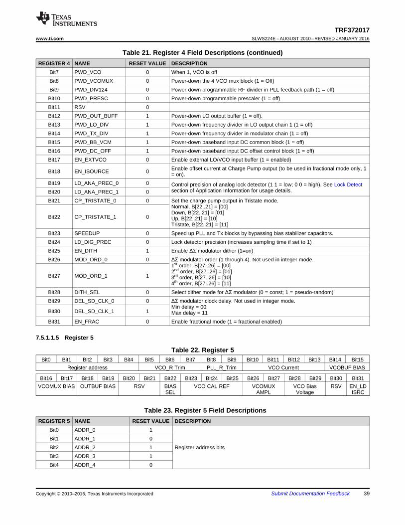
TRF372017www.ti.com SLWS224E –AUGUST 2010–REVISED JANUARY 2016
Table 21. Register 4 Field Descriptions (continued)REGISTER 4 NAME RESET VALUE DESCRIPTION
Bit7 PWD_VCO 0 When 1, VCO is offBit8 PWD_VCOMUX 0 Power-down the 4 VCO mux block (1 = Off)Bit9 PWD_DIV124 0 Power-down programmable RF divider in PLL feedback path (1 = off)Bit10 PWD_PRESC 0 Power-down programmable prescaler (1 = off)Bit11 RSV 0Bit12 PWD_OUT_BUFF 1 Power-down LO output buffer (1 = off).Bit13 PWD_LO_DIV 1 Power-down frequency divider in LO output chain 1 (1 = off)Bit14 PWD_TX_DIV 1 Power-down frequency divider in modulator chain (1 = off)Bit15 PWD_BB_VCM 1 Power-down baseband input DC common block (1 = off)Bit16 PWD_DC_OFF 1 Power-down baseband input DC offset control block (1 = off)Bit17 EN_EXTVCO 0 Enable external LO/VCO input buffer (1 = enabled)
Enable offset current at Charge Pump output (to be used in fractional mode only, 1Bit18 EN_ISOURCE 0 = on).Bit19 LD_ANA_PREC_0 0 Control precision of analog lock detector (1 1 = low; 0 0 = high). See Lock Detect
section of Application Information for usage details.Bit20 LD_ANA_PREC_1 0Bit21 CP_TRISTATE_0 0 Set the charge pump output in Tristate mode.
Normal, B[22..21] = [00]Down, B[22..21] = [01]
Bit22 CP_TRISTATE_1 0 Up, B[22..21] = [10]Tristate, B[22..21] = [11]
Bit23 SPEEDUP 0 Speed up PLL and Tx blocks by bypassing bias stabilizer capacitors.Bit24 LD_DIG_PREC 0 Lock detector precision (increases sampling time if set to 1)Bit25 EN_DITH 1 Enable ΔΣ modulator dither (1=on)Bit26 MOD_ORD_0 0 ΔΣ modulator order (1 through 4). Not used in integer mode.
1st order, B[27..26] = [00]2nd order, B[27..26] = [01]
Bit27 MOD_ORD_1 1 3rd order, B[27..26] = [10]4th order, B[27..26] = [11]
Bit28 DITH_SEL 0 Select dither mode for ΔΣ modulator (0 = const; 1 = pseudo-random)Bit29 DEL_SD_CLK_0 0 ΔΣ modulator clock delay. Not used in integer mode.
Min delay = 00Bit30 DEL_SD_CLK_1 1 Max delay = 11Bit31 EN_FRAC 0 Enable fractional mode (1 = fractional enabled)
7.5.1.1.5 Register 5
Table 22. Register 5Bit0 Bit1 Bit2 Bit3 Bit4 Bit5 Bit6 Bit7 Bit8 Bit9 Bit10 Bit11 Bit12 Bit13 Bit14 Bit15
Register address VCO_R Trim PLL_R_Trim VCO Current VCOBUF BIAS
Bit16 Bit17 Bit18 Bit19 Bit20 Bit21 Bit22 Bit23 Bit24 Bit25 Bit26 Bit27 Bit28 Bit29 Bit30 Bit31VCOMUX BIAS OUTBUF BIAS RSV BIAS VCO CAL REF VCOMUX VCO Bias RSV EN_LD
SEL AMPL Voltage ISRC
Table 23. Register 5 Field DescriptionsREGISTER 5 NAME RESET VALUE DESCRIPTION
Bit0 ADDR_0 1Bit1 ADDR_1 0Bit2 ADDR_2 1 Register address bitsBit3 ADDR_3 1Bit4 ADDR_4 0
Copyright © 2010–2016, Texas Instruments Incorporated Submit Documentation Feedback 39
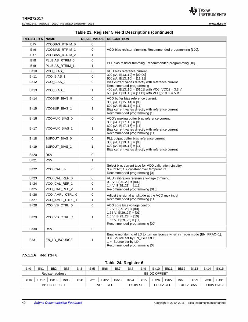
TRF372017SLWS224E –AUGUST 2010–REVISED JANUARY 2016 www.ti.com
Table 23. Register 5 Field Descriptions (continued)REGISTER 5 NAME RESET VALUE DESCRIPTION
Bit5 VCOBIAS_RTRIM_0 0Bit6 VCOBIAS_RTRIM_1 0 VCO bias resistor trimming. Recommended programming [100].Bit7 VCOBIAS_RTRIM_2 1Bit8 PLLBIAS_RTRIM_0 0
PLL bias resistor trimming. Recommended programming [10].Bit9 PLLBIAS_RTRIM_1 1Bit10 VCO_BIAS_0 0 VCO bias reference current.
300 µA, B[13..10] = [00 00]Bit11 VCO_BIAS_1 0 600 µA, B[13..10] = [11 11]Bit12 VCO_BIAS_2 0 Bias current varies directly with reference current
Recommended programming400 µA, B[13..10] = [0101] with VCC_VCO2 = 3.3 VBit13 VCO_BIAS_3 1600 µA, B[13..10] = [1111] with VCC_VCO2 = 5 V
Bit14 VCOBUF_BIAS_0 0 VCO buffer bias reference current.300 µA, B[15..14] = [00]600 µA, B[15..14] = [11]
Bit15 VCOBUF_BIAS_1 1 Bias current varies directly with reference currentRecommended programming [10]
Bit16 VCOMUX_BIAS_0 0 VCO’s muxing buffer bias reference current.300 µA, B[17..16] = [00]600 µA, B[17..16] = [11]
Bit17 VCOMUX_BIAS_1 1 Bias current varies directly with reference currentRecommended programming [11]
Bit18 BUFOUT_BIAS_0 0 PLL output buffer bias reference current.300 µA, B[19..18] = [00]600 µA, B[19..18] = [11]Bit19 BUFOUT_BIAS_1 1Bias current varies directly with reference current
Bit20 RSV 0Bit21 RSV 1
Select bias current type for VCO calibration circuitryBit22 VCO_CAL_IB 0 0 = PTAT; 1 = constant over temperature
Recommended programming [0]Bit23 VCO_CAL_REF_0 0 VCO calibration reference voltage trimming.
0.9 V, B[25..23] = [000]Bit24 VCO_CAL_REF_1 0 1.4 V, B[25..23] = [111]Bit25 VCO_CAL_REF_2 1 Recommended programming [010]Bit26 VCO_AMPL_CTRL_0 0 Adjust the signal amplitude at the VCO mux input
Recommended programming [11]Bit27 VCO_AMPL_CTRL_1 1Bit28 VCO_VB_CTRL_0 0 VCO core bias voltage control
1.2 V, B[29..28] = [00]1.35 V, B[29..28] = [01]1.5 V, B[29..28] = [10]Bit29 VCO_VB_CTRL _1 11.65 V, B[29..28] = [11]Recommended programming [00]
Bit30 RSV 0Enable monitoring of LD to turn on Isource when in frac-n mode (EN_FRAC=1).0 = ISource set by EN_ISOURCE.Bit31 EN_LD_ISOURCE 1 1 = ISource set by LD.Recommended programming [0]
7.5.1.1.6 Register 6
Table 24. Register 6Bit0 Bit1 Bit2 Bit3 Bit4 Bit5 Bit6 Bit7 Bit8 Bit9 Bit10 Bit11 Bit12 Bit13 Bit14 Bit15
Register address BB DC OFFSET
Bit16 Bit17 Bit18 Bit19 Bit20 Bit21 Bit22 Bit23 Bit24 Bit25 Bit26 Bit27 Bit28 Bit29 Bit30 Bit31BB DC OFFSET VREF SEL TXDIV SEL LODIV SEL TXDIV BIAS LODIV BIAS
40 Submit Documentation Feedback Copyright © 2010–2016, Texas Instruments Incorporated
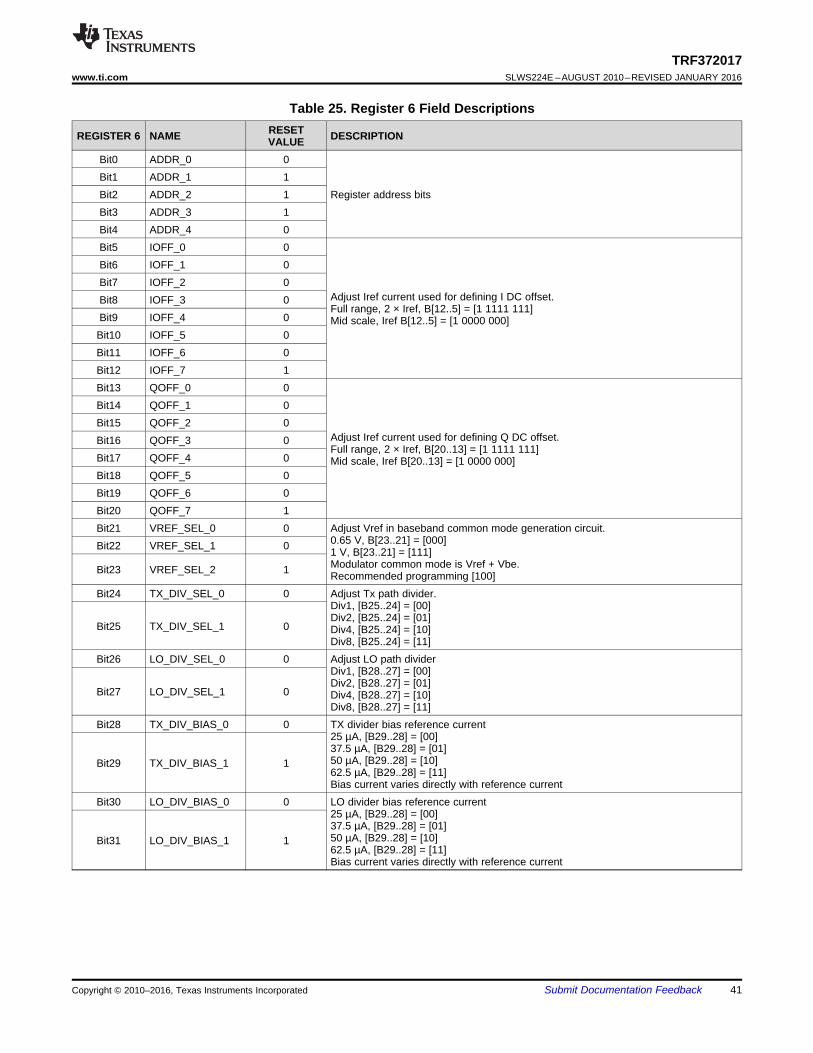
TRF372017www.ti.com SLWS224E –AUGUST 2010–REVISED JANUARY 2016
Table 25. Register 6 Field DescriptionsRESETREGISTER 6 NAME DESCRIPTIONVALUE
Bit0 ADDR_0 0Bit1 ADDR_1 1Bit2 ADDR_2 1 Register address bitsBit3 ADDR_3 1Bit4 ADDR_4 0Bit5 IOFF_0 0Bit6 IOFF_1 0Bit7 IOFF_2 0
Adjust Iref current used for defining I DC offset.Bit8 IOFF_3 0Full range, 2 × Iref, B[12..5] = [1 1111 111]
Bit9 IOFF_4 0 Mid scale, Iref B[12..5] = [1 0000 000]Bit10 IOFF_5 0Bit11 IOFF_6 0Bit12 IOFF_7 1Bit13 QOFF_0 0Bit14 QOFF_1 0Bit15 QOFF_2 0
Adjust Iref current used for defining Q DC offset.Bit16 QOFF_3 0Full range, 2 × Iref, B[20..13] = [1 1111 111]
Bit17 QOFF_4 0 Mid scale, Iref B[20..13] = [1 0000 000]Bit18 QOFF_5 0Bit19 QOFF_6 0Bit20 QOFF_7 1Bit21 VREF_SEL_0 0 Adjust Vref in baseband common mode generation circuit.
0.65 V, B[23..21] = [000]Bit22 VREF_SEL_1 0 1 V, B[23..21] = [111]Modulator common mode is Vref + Vbe.Bit23 VREF_SEL_2 1 Recommended programming [100]
Bit24 TX_DIV_SEL_0 0 Adjust Tx path divider.Div1, [B25..24] = [00]Div2, [B25..24] = [01]
Bit25 TX_DIV_SEL_1 0 Div4, [B25..24] = [10]Div8, [B25..24] = [11]
Bit26 LO_DIV_SEL_0 0 Adjust LO path dividerDiv1, [B28..27] = [00]Div2, [B28..27] = [01]
Bit27 LO_DIV_SEL_1 0 Div4, [B28..27] = [10]Div8, [B28..27] = [11]
Bit28 TX_DIV_BIAS_0 0 TX divider bias reference current25 µA, [B29..28] = [00]37.5 µA, [B29..28] = [01]50 µA, [B29..28] = [10]Bit29 TX_DIV_BIAS_1 162.5 µA, [B29..28] = [11]Bias current varies directly with reference current
Bit30 LO_DIV_BIAS_0 0 LO divider bias reference current25 µA, [B29..28] = [00]37.5 µA, [B29..28] = [01]50 µA, [B29..28] = [10]Bit31 LO_DIV_BIAS_1 162.5 µA, [B29..28] = [11]Bias current varies directly with reference current
Copyright © 2010–2016, Texas Instruments Incorporated Submit Documentation Feedback 41
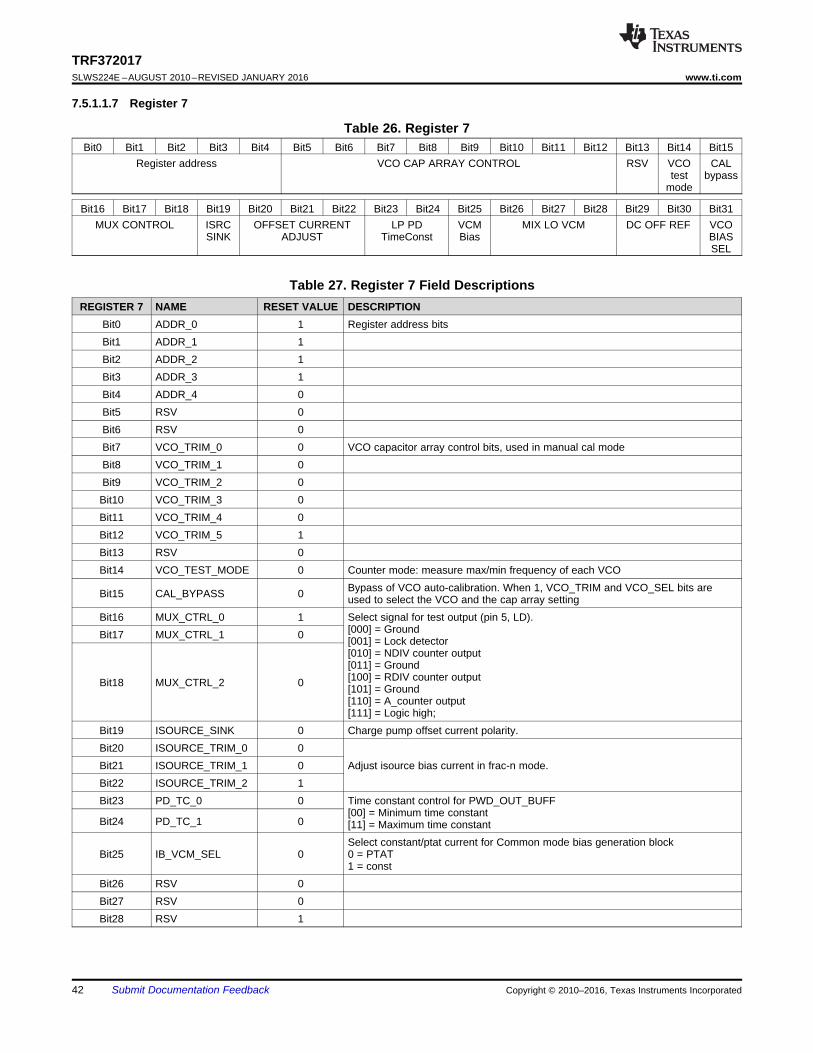
TRF372017SLWS224E –AUGUST 2010–REVISED JANUARY 2016 www.ti.com
7.5.1.1.7 Register 7
Table 26. Register 7Bit0 Bit1 Bit2 Bit3 Bit4 Bit5 Bit6 Bit7 Bit8 Bit9 Bit10 Bit11 Bit12 Bit13 Bit14 Bit15
Register address VCO CAP ARRAY CONTROL RSV VCO CALtest bypass
mode
Bit16 Bit17 Bit18 Bit19 Bit20 Bit21 Bit22 Bit23 Bit24 Bit25 Bit26 Bit27 Bit28 Bit29 Bit30 Bit31MUX CONTROL ISRC OFFSET CURRENT LP PD VCM MIX LO VCM DC OFF REF VCO
SINK ADJUST TimeConst Bias BIASSEL
Table 27. Register 7 Field DescriptionsREGISTER 7 NAME RESET VALUE DESCRIPTION
Bit0 ADDR_0 1 Register address bitsBit1 ADDR_1 1Bit2 ADDR_2 1Bit3 ADDR_3 1Bit4 ADDR_4 0Bit5 RSV 0Bit6 RSV 0Bit7 VCO_TRIM_0 0 VCO capacitor array control bits, used in manual cal modeBit8 VCO_TRIM_1 0Bit9 VCO_TRIM_2 0Bit10 VCO_TRIM_3 0Bit11 VCO_TRIM_4 0Bit12 VCO_TRIM_5 1Bit13 RSV 0Bit14 VCO_TEST_MODE 0 Counter mode: measure max/min frequency of each VCO
Bypass of VCO auto-calibration. When 1, VCO_TRIM and VCO_SEL bits areBit15 CAL_BYPASS 0 used to select the VCO and the cap array settingBit16 MUX_CTRL_0 1 Select signal for test output (pin 5, LD).
[000] = GroundBit17 MUX_CTRL_1 0 [001] = Lock detector[010] = NDIV counter output[011] = Ground[100] = RDIV counter outputBit18 MUX_CTRL_2 0 [101] = Ground[110] = A_counter output[111] = Logic high;
Bit19 ISOURCE_SINK 0 Charge pump offset current polarity.Bit20 ISOURCE_TRIM_0 0Bit21 ISOURCE_TRIM_1 0 Adjust isource bias current in frac-n mode.Bit22 ISOURCE_TRIM_2 1Bit23 PD_TC_0 0 Time constant control for PWD_OUT_BUFF
[00] = Minimum time constantBit24 PD_TC_1 0 [11] = Maximum time constant
Select constant/ptat current for Common mode bias generation blockBit25 IB_VCM_SEL 0 0 = PTAT
1 = constBit26 RSV 0Bit27 RSV 0Bit28 RSV 1
42 Submit Documentation Feedback Copyright © 2010–2016, Texas Instruments Incorporated

TRF372017www.ti.com SLWS224E –AUGUST 2010–REVISED JANUARY 2016
Table 27. Register 7 Field Descriptions (continued)REGISTER 7 NAME RESET VALUE DESCRIPTION
Bit29 DCOFFSET_I_0 0 Adjust BB input DC offset Iref50 µA, B[27..26] = [00]100 µA, B[27..26] = [01]
Bit30 DCOFFSET_I_1 1 150 µA, B[27..26] = [10]200 µA, B[27..26] = [11]Select VCO_BIAS trim settings stored in EEPROM0 = Use EEPROM settings if parity check is 1; otherwise, use SPI settingsBit31 VCO_BIAS_SEL 0 1 = Use SPI settingsRecommended programming [1]
7.5.1.2 Readback ModeRegister 0 functions as a Readback register. TRF372017 implements the capability to read-back the content ofany serial programming interface register by initializing register 0.
Each read-back is composed by two phases: writing followed by the actual reading of the internal data. This isshown in the timing diagram in Figure 2. During the writing phase, a command is sent to TRF372017 register 0to set it in read-back mode and to specify which register is to be read. In the proper reading phase, at each risingclock edge, the internal data is transferred into the RDBK pin and can be read at the following falling edge (LSBfirst). The first clock after the LE goes high (end of writing cycle) is idle and the following 32 clocks pulsestransfer the internal register content to the RDBK pin.
7.5.1.2.1 Readback From the Internal Registers Banks
TRF372017 integrates 8 registers: Register 0 (000) to Register 7 (111). Registers 1 through 7 are used to set-upand control the TRF372017 functionalities, while register 0 is used for the readback function.
The latter register must be programmed with a specific command that sets TRF372017 in read-back mode andspecifies the register to be read:• Set B[31] to 1 to put TRF372017 in read-back mode.• Set B[30,28] equal to the address of the register to be read (000 to 111).• Set B27 to control the VCO frequency counter in VCO test mode.
7.5.1.2.1.1 Register 0 Write
Table 28. Register 0 WriteNAME RESET VALUE DESCRIPTION
B0 ADDR<0> 0B1 ADDR<1> 0
ADDRESS B2 ADDR<2> 0 Register 0 to be programmed to set TRF372017 in readback mode.BITSB3 ADDR<3> 1B4 ADDR<4> 0
Copyright © 2010–2016, Texas Instruments Incorporated Submit Documentation Feedback 43

TRF372017SLWS224E –AUGUST 2010–REVISED JANUARY 2016 www.ti.com
Table 28. Register 0 Write (continued)NAME RESET VALUE DESCRIPTION
B5 N/C 0B6 N/C 0B7 N/C 0B8 N/C 0B9 N/C 0B10 N/C 0B11 N/C 0B12 N/C 0B13 N/C 0B14 N/C 0B15 N/C 0B16 N/C 0B17 N/C 0B18 N/C 0B19 N/C 0DATA FIELDB20 N/C 0B21 N/C 0B22 N/C 0B23 N/C 0B24 N/C 0B25 N/C 0B26 N/C 0
Select Readback for VCO maximum frequency or minimumfrequency.B27 COUNT_MODE_MUX_SEL 0 0 = Max1 = Min
B28 RB_REG<0> X 3 LSB’s of the address for the register that is being readB29 RB_REG<1> X Reg 0, B[30..28] = [000]
Reg 7, B[30..28] = [111]B30 RB_REG<2> XB31 RB_ENABLE 1 1 ≥ Put the device in Readback Mode
The contents of any register specified in RB_REG can be read back during the read cycle, including register 0.
Bit0 Bit1 Bit2 Bit3 Bit4 Bit5 Bit6 Bit7 Bit8 Bit9 Bit10 Bit11 Bit12Register address CHIP_ID NU R_SAT_ERR
Bit13 Bit14 Bit15 Bit16 Bit17 Bit18 Bit19 Bit20 Bit21 Bit22 Bit23 Bit24 Bit25 Bit26 Bit27 Bit28 Bit29 Bit30COUNT0-7/VCO_TRM COUNT8-10/VCO_SEL COUNT11-17
Bit31COUNT_MODE-MUX-SEL
REGISTER 0 NAME RESET VALUE DESCRIPTIONBit0 ADDR_0 0 Register address bitsBit1 ADDR_1 0Bit2 ADDR_2 0Bit3 ADDR_3 1Bit4 ADDR_4 0Bit5 CHIP_ID_0 1Bit6 CHIP_ID_1 1Bit7 NU x
44 Submit Documentation Feedback Copyright © 2010–2016, Texas Instruments Incorporated

TRF372017www.ti.com SLWS224E –AUGUST 2010–REVISED JANUARY 2016
REGISTER 0 NAME RESET VALUE DESCRIPTIONBit8 NU xBit9 NU xBit10 NU xBit11 NU xBit12 R_SAT_ERR x Error flag for calibration speedBit13 count_0/NU xBit14 count_1/NU xBit15 count_2/VCO_TRIM_0 xBit16 count_3/VCO_TRIM_1 x B[30..13] = VCO frequency counter high when
COUNT_MODE_MUX_SEL = 0 and VCO_TEST_MODE = 1Bit17 count_4/VCO_TRIM_2 xBit18 count_5/VCO_TRIM_3 xBit19 count_6/VCO_TRIM_4 xBit20 count_7/VCO_TRIM_5 xBit21 count_8/NU x
B[30..13] = VCO frequency counter low whenBit22 count_9/VCO_sel_0 x COUNT_MODE_MUX_SEL = 1 and VCO_TEST_MODE = 1Bit23 count_10/VCO_sel_1 xBit24 count<11> xBit25 count<12> xBit26 count<13> x B[20..15] = Autocal results for VCO_TRIM,Bit27 count<14> x B[23..22] = Autocal results for VCO_SEL when
VCO_TEST_MODE = 0Bit28 count<15> xBit29 count<16> xBit30 count<17> x
0 = Minimum frequencyBit31 COUNT_MODE_MUX_SEL x 1 = Maximum frequency
Copyright © 2010–2016, Texas Instruments Incorporated Submit Documentation Feedback 45

VCC_LO1
VCC_DIG
GND_DIG
GNDLD
BBQ_N
BBQ_P
GND
RS
VD
GN
D
RF
OU
T
VC
C_
MIX
GN
D
LO_OUT_PLO_OUT_N
CLK
DA
TA
LE
EXT_VCO
BBI_N
BBI_P
GND
RE
FIN
GN
D
VC
C_
PL
L
CP
_O
UT
GN
D
GN
D
VT
UN
E
VCC_VCO2
GN
D
VCC_LO2
GND
GN
D
VC
C_
D2S
GN
D
GN
D
GND
PS
RDBK
GND
GN
D
GN
D
GN
D
GND
GND
VCC_VCO1
SC
AN
_E
N
75
4.7 pF
PS
LE
DATA
RDBK
CLK
22 pF
REFIN
R3
R2
C1 C2 C3
R4
C41 mF 4.7 pF
+3.3 V
FB-1K
Loop Filter:
values described
in table
EXT_VCO
1 mF 4.7 pF
FB-1K
+3.3 V
1 mF 4.7 pF
FB-1K
+3.3 V/+5.0 V
100 pF 4.7 pF
FB-1K
+3.3 V
+3.3 V
Baseband interface
described in application information
BBI_N
BBI_P
1.8 pF 1000 pF 1 mF
75
+3.3 V
1.8 pF 1000 pF 1 mF
LO_OUT_P
LO_OUT_N
4.7 pF
4.7 pF
100 pF 4.7 pF
FB-1K
+5.0 V
100 pF 4.7 pF
FB-1K
+5.0 V
100 pF1 mF
FB-1K
+3.3 V
100 pF4.7 pF
FB-1K
+3.3V
LD
BBQ_N
BBQ_P
Baseband interface
described in application information
22 pFRFOUT
NC
TRF372017SLWS224E –AUGUST 2010–REVISED JANUARY 2016 www.ti.com
8 Application and Implementation
NOTEInformation in the following applications sections is not part of the TI componentspecification, and TI does not warrant its accuracy or completeness. TI’s customers areresponsible for determining suitability of components for their purposes. Customers shouldvalidate and test their design implementation to confirm system functionality.
8.1 Application InformationThe TRF372017 is suited for quadrature up-conversion applications such as wireless radio transmitters.
8.2 Typical Application
46 Submit Documentation Feedback Copyright © 2010–2016, Texas Instruments Incorporated

90.9 ΩDAC3283
10 nH
125 Ω
450 Ω500 Ω
1mF
GND
+5 V
2.2 pF
DNI
68 nH
2.7 pF
60.4 Ω
TRF3720
125 Ω
+5 V
450 Ω500 Ω
1mF
GND
68 nH
60.4 Ω
10 nH
TRF372017www.ti.com SLWS224E –AUGUST 2010–REVISED JANUARY 2016
Typical Application (continued)8.2.1 Design RequirementsTable 29 shows the design requirements for this application.
Table 29. Quadrature Up-Converter Design Requirements for Wireless Transmitter ApplicationPARAMETER REQUIREMENT (1) TRF372017 PERFORMANCE
Gain –5 to 0 dB –3.1 dBNoise figure, NF <21 dB 19 dB3rd order intercept (IIP3) >+20 dBm +25 dBm1dB compression (P1dB) >+10 dBm +11.5 dBmACPR >70 dBc 75 dBcRF output frequency range 1500 to 2500 MHz 300 to 4300 MHzLO input frequency range 1000 to 3000 MHz 300 to 4800 MHzIF input frequency range DC - 150 MHz DC - 1 GHzLO phase noise <–130 dBc/Hz, 1 GHz, 1 MHz offset –137 dBc/Hz, 1 GHz, 1 MHz offset
(1) These requirements represent a hypothetical application and do not reflect the performance of the TRF372017.
8.2.2 Detailed Design Procedure
8.2.2.1 DAC Interfacing With External Baseband Bias VoltageCommon-mode voltage on the baseband inputs can be generated either internally or externally. An externalinterface must provide 1.7-V DC and any necessary filtering. A typical interface to a DAC device is shown inFigure 86.
Figure 86. DAC to TRF372017 Interface With External VCM Generation
8.2.2.2 DAC Interface Using Internal VCM GenerationA typical DAC to TRF372017 interface using internal VCM generation is shown in Figure 87.
Copyright © 2010–2016, Texas Instruments Incorporated Submit Documentation Feedback 47

+3.3 V
75
47 pF
LO_OUT_P
LO_OUT_N
75
47 pF
DAC3283
115
634
GND
+5 V
2.2 pF
DNI
68 nH
2.7 pF
60.4
TRF3720
115
+5 V
634
GND
68 nH
60.4
90.9
10 nH
10 nH
1 mF
1 mF
TRF372017SLWS224E –AUGUST 2010–REVISED JANUARY 2016 www.ti.com
Figure 87. DAC to TRF372017 Interface With Internal VCM Generation
8.2.2.3 LO OutputsThe LO outputs are open collector outputs. They require a pullup to VCC. 75-Ω pullup resistors to VCC with localdecoupling provides a good broadband match and is shown in an example circuit in Figure 88. An inductor pullupin parallel with a cap can provide a tuned load for excellent narrowband load matching.
Figure 88. Example LO_OUT Circuit for Broadband Operation
8.2.2.4 Loop FilterLoop filter design is critical for achieving low closed loop phase noise. Some typical loop filter component valuesare given in Table 30, referenced to designators in Figure 89. These loop filters are designed using charge pumpcurrent of 1.94 mA to minimize noise.
Table 30. Typical Loop Filter ComponentsfPFD (MHz) C1 (pF) C2 (pF) R2 (kΩ) C3 (pF) R3 (kΩ) C4 (pF) R4 (kΩ)
40 1000 10000 0.47 39 1.4 1.8 3.31.6 47 560 10 4.7 5 open 06.4 100 1000 5 20 5 open 010 270 4700 1.5 4700 1.5 open 0
30.72 2200 20000 0.47 220 0.475 220 0.475
48 Submit Documentation Feedback Copyright © 2010–2016, Texas Instruments Incorporated
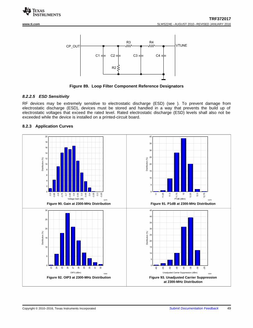
Dis
trib
ution
(%)
0
5
10
15
20
25
30
23
24
25
26
27
28
29
30
31
32
OIP3 (dBm)G080
Dis
trib
ution
(%)
0
5
10
15
20
25
30
35
40
45
-60
-55
-50
-45
-40
-35
-30
-25
Unadjusted Carrier Suppression (dBm)G081
Dis
trib
ution
(%)
0
2
4
6
8
10
12
14
16
18
20
-3.9
-3.8
5
-3.8
-3.7
5
-3.7
-3.6
5
-3.6
-3.5
5
-3.5
-3.4
5
-3.4
-3.3
5
-3.3
-3.2
5
Voltage Gain (dB)G078
Dis
trib
ution
(%)
0
5
10
15
20
25
30
35
40
11
11.2
5
11.5
11.7
5
12
12.2
5
12.5
12.7
5
P1dB (dBm)G079
R3
R2
C1 C2 C3
R4
C4
CP_OUT VTUNE
TRF372017www.ti.com SLWS224E –AUGUST 2010–REVISED JANUARY 2016
Figure 89. Loop Filter Component Reference Designators
8.2.2.5 ESD SensitivityRF devices may be extremely sensitive to electrostatic discharge (ESD) (see ). To prevent damage fromelectrostatic discharge (ESD), devices must be stored and handled in a way that prevents the build up ofelectrostatic voltages that exceed the rated level. Rated electrostatic discharge (ESD) levels shall also not beexceeded while the device is installed on a printed-circuit board.
8.2.3 Application Curves
Figure 90. Gain at 2300-MHz Distribution Figure 91. P1dB at 2300-MHz Distribution
Figure 92. OIP3 at 2300-MHz Distribution Figure 93. Unadjusted Carrier Suppressionat 2300-MHz Distribution
Copyright © 2010–2016, Texas Instruments Incorporated Submit Documentation Feedback 49

Dis
trib
ution
(%)
0
5
10
15
20
25
30
35
40
45
35
40
45
50
55
60
65
70
Unadjusted Sideband Suppression (dBc)G082
TRF372017SLWS224E –AUGUST 2010–REVISED JANUARY 2016 www.ti.com
Figure 94. Unadjusted Sideband Suppressionat 2300-MHz Distribution
9 Power Supply RecommendationsThe TRF372017 must be supplied with a low noise 5-V or 3.3-V supply as required. Each supply pin mustgenerally be isolated from the main power bus with a ferrite or other noise filtering component.
50 Submit Documentation Feedback Copyright © 2010–2016, Texas Instruments Incorporated

TRF372017www.ti.com SLWS224E –AUGUST 2010–REVISED JANUARY 2016
10 Layout
10.1 Layout GuidelinesLayout of the application board significantly impacts the analog performance of the TRF372017 device. Noiseand high-speed signals must be prevented from leaking onto power-supply pins or analog signals. Follow theserecommendations:1. Place supply decoupling capacitors physically close to the device, on the same side of the board. Each
supply pin must be isolated with a ferrite bead.2. Maintain a continuous ground plane in the vicinity of the device and as return paths for all high-speed signal
lines. Place reference plane vias or decoupling capacitors near any signal line reference transition.3. The pad on the bottom of the device must be electrically grounded. Connect GND pins directly to the pad on
the surface layer. Connect the GND pins and pad directly to surface ground where possible.4. Power planes must not overlap each other or high-speed signal lines.5. Isolate REF_IN routing from loop filter lines, control lines, and other high-speed lines.
See Figure 95 for an example of critical component layout (for the top PCB layer).
10.2 Layout Example
Figure 95. Critical Layout of the TRF372017 EVM Board
Copyright © 2010–2016, Texas Instruments Incorporated Submit Documentation Feedback 51

TRF372017SLWS224E –AUGUST 2010–REVISED JANUARY 2016 www.ti.com
11 Device and Documentation Support
11.1 Device Support
11.1.1 Third-Party Products DisclaimerTI'S PUBLICATION OF INFORMATION REGARDING THIRD-PARTY PRODUCTS OR SERVICES DOES NOTCONSTITUTE AN ENDORSEMENT REGARDING THE SUITABILITY OF SUCH PRODUCTS OR SERVICESOR A WARRANTY, REPRESENTATION OR ENDORSEMENT OF SUCH PRODUCTS OR SERVICES, EITHERALONE OR IN COMBINATION WITH ANY TI PRODUCT OR SERVICE.
11.2 Community ResourcesThe following links connect to TI community resources. Linked contents are provided "AS IS" by the respectivecontributors. They do not constitute TI specifications and do not necessarily reflect TI's views; see TI's Terms ofUse.
TI E2E™ Online Community TI's Engineer-to-Engineer (E2E) Community. Created to foster collaborationamong engineers. At e2e.ti.com, you can ask questions, share knowledge, explore ideas and helpsolve problems with fellow engineers.
Design Support TI's Design Support Quickly find helpful E2E forums along with design support tools andcontact information for technical support.
11.3 TrademarksE2E is a trademark of Texas Instruments.All other trademarks are the property of their respective owners.
11.4 Electrostatic Discharge CautionThese devices have limited built-in ESD protection. The leads should be shorted together or the device placed in conductive foamduring storage or handling to prevent electrostatic damage to the MOS gates.
11.5 GlossarySLYZ022 — TI Glossary.
This glossary lists and explains terms, acronyms, and definitions.
12 Mechanical, Packaging, and Orderable InformationThe following pages include mechanical, packaging, and orderable information. This information is the mostcurrent data available for the designated devices. This data is subject to change without notice and revision ofthis document. For browser-based versions of this data sheet, refer to the left-hand navigation.
52 Submit Documentation Feedback Copyright © 2010–2016, Texas Instruments Incorporated

PACKAGE OPTION ADDENDUM
www.ti.com 10-Dec-2020
Addendum-Page 1
PACKAGING INFORMATION
Orderable Device Status(1)
Package Type PackageDrawing
Pins PackageQty
Eco Plan(2)
Lead finish/Ball material
(6)
MSL Peak Temp(3)
Op Temp (°C) Device Marking(4/5)
Samples
TRF372017IRGZR ACTIVE VQFN RGZ 48 2500 RoHS & Green NIPDAU Level-2-260C-1 YEAR -40 to 85 TRF372017IRGZ
TRF372017IRGZT ACTIVE VQFN RGZ 48 250 RoHS & Green NIPDAU Level-2-260C-1 YEAR -40 to 85 TRF372017IRGZ
(1) The marketing status values are defined as follows:ACTIVE: Product device recommended for new designs.LIFEBUY: TI has announced that the device will be discontinued, and a lifetime-buy period is in effect.NRND: Not recommended for new designs. Device is in production to support existing customers, but TI does not recommend using this part in a new design.PREVIEW: Device has been announced but is not in production. Samples may or may not be available.OBSOLETE: TI has discontinued the production of the device.
(2) RoHS: TI defines "RoHS" to mean semiconductor products that are compliant with the current EU RoHS requirements for all 10 RoHS substances, including the requirement that RoHS substancedo not exceed 0.1% by weight in homogeneous materials. Where designed to be soldered at high temperatures, "RoHS" products are suitable for use in specified lead-free processes. TI mayreference these types of products as "Pb-Free".RoHS Exempt: TI defines "RoHS Exempt" to mean products that contain lead but are compliant with EU RoHS pursuant to a specific EU RoHS exemption.Green: TI defines "Green" to mean the content of Chlorine (Cl) and Bromine (Br) based flame retardants meet JS709B low halogen requirements of <=1000ppm threshold. Antimony trioxide basedflame retardants must also meet the <=1000ppm threshold requirement.
(3) MSL, Peak Temp. - The Moisture Sensitivity Level rating according to the JEDEC industry standard classifications, and peak solder temperature.
(4) There may be additional marking, which relates to the logo, the lot trace code information, or the environmental category on the device.
(5) Multiple Device Markings will be inside parentheses. Only one Device Marking contained in parentheses and separated by a "~" will appear on a device. If a line is indented then it is a continuationof the previous line and the two combined represent the entire Device Marking for that device.
(6) Lead finish/Ball material - Orderable Devices may have multiple material finish options. Finish options are separated by a vertical ruled line. Lead finish/Ball material values may wrap to twolines if the finish value exceeds the maximum column width.
Important Information and Disclaimer:The information provided on this page represents TI's knowledge and belief as of the date that it is provided. TI bases its knowledge and belief on informationprovided by third parties, and makes no representation or warranty as to the accuracy of such information. Efforts are underway to better integrate information from third parties. TI has taken andcontinues to take reasonable steps to provide representative and accurate information but may not have conducted destructive testing or chemical analysis on incoming materials and chemicals.TI and TI suppliers consider certain information to be proprietary, and thus CAS numbers and other limited information may not be available for release.
In no event shall TI's liability arising out of such information exceed the total purchase price of the TI part(s) at issue in this document sold by TI to Customer on an annual basis.
PACKAGE OPTION ADDENDUM
www.ti.com 10-Dec-2020
Addendum-Page 2
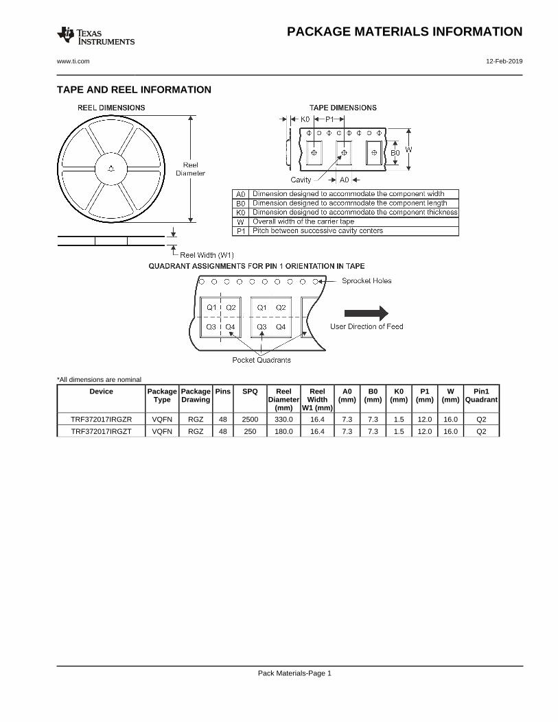
TAPE AND REEL INFORMATION
*All dimensions are nominal
Device PackageType
PackageDrawing
Pins SPQ ReelDiameter
(mm)
ReelWidth
W1 (mm)
A0(mm)
B0(mm)
K0(mm)
P1(mm)
W(mm)
Pin1Quadrant
TRF372017IRGZR VQFN RGZ 48 2500 330.0 16.4 7.3 7.3 1.5 12.0 16.0 Q2
TRF372017IRGZT VQFN RGZ 48 250 180.0 16.4 7.3 7.3 1.5 12.0 16.0 Q2
PACKAGE MATERIALS INFORMATION
www.ti.com 12-Feb-2019
Pack Materials-Page 1

*All dimensions are nominal
Device Package Type Package Drawing Pins SPQ Length (mm) Width (mm) Height (mm)
TRF372017IRGZR VQFN RGZ 48 2500 350.0 350.0 43.0
TRF372017IRGZT VQFN RGZ 48 250 213.0 191.0 55.0
PACKAGE MATERIALS INFORMATION
www.ti.com 12-Feb-2019
Pack Materials-Page 2

www.ti.com
GENERIC PACKAGE VIEW
Images above are just a representation of the package family, actual package may vary.Refer to the product data sheet for package details.
VQFN - 1 mm max heightRGZ 48PLASTIC QUADFLAT PACK- NO LEAD7 x 7, 0.5 mm pitch
4224671/A

www.ti.com
PACKAGE OUTLINE
C
SEE TERMINALDETAIL
48X 0.300.18
5.6 0.1
48X 0.50.3
1.00.8
(0.2) TYP
0.050.00
44X 0.5
2X5.5
2X 5.5
B 7.16.9
A
7.16.9
0.300.18
0.50.3
VQFN - 1 mm max heightRGZ0048DPLASTIC QUAD FLATPACK - NO LEAD
4219046/B 11/2019
PIN 1 INDEX AREA
0.08 C
SEATING PLANE
1
1225
36
13 24
48 37
(OPTIONAL)PIN 1 ID 0.1 C A B
0.05
EXPOSEDTHERMAL PAD
49 SYMM
SYMM
NOTES: 1. All linear dimensions are in millimeters. Any dimensions in parenthesis are for reference only. Dimensioning and tolerancing per ASME Y14.5M. 2. This drawing is subject to change without notice. 3. The package thermal pad must be soldered to the printed circuit board for thermal and mechanical performance.
SCALE 1.900
DETAILOPTIONAL TERMINAL
TYPICAL

www.ti.com
EXAMPLE BOARD LAYOUT
10X(1.33)
10X (1.33) 6X (1.22)
0.07 MINALL AROUND
0.07 MAXALL AROUND
48X (0.24)
48X (0.6)
( 0.2) TYPVIA
44X (0.5)
(6.8)
(6.8)
6X(1.22)
( 5.6)
(R0.05)TYP
VQFN - 1 mm max heightRGZ0048DPLASTIC QUAD FLATPACK - NO LEAD
4219046/B 11/2019
SYMM
1
12
13 24
25
36
3748
SYMM
LAND PATTERN EXAMPLEEXPOSED METAL SHOWN
SCALE:12X
49
NOTES: (continued) 4. This package is designed to be soldered to a thermal pad on the board. For more information, see Texas Instruments literature number SLUA271 (www.ti.com/lit/slua271).5. Vias are optional depending on application, refer to device data sheet. If any vias are implemented, refer to their locations shown on this view. It is recommended that vias under paste be filled, plugged or tented.
SOLDER MASKOPENING
METAL UNDERSOLDER MASK
SOLDER MASKDEFINED
EXPOSED METALMETAL
SOLDER MASKOPENING
SOLDER MASK DETAILS
NON SOLDER MASKDEFINED
(PREFERRED)
EXPOSED METAL

www.ti.com
EXAMPLE STENCIL DESIGN
48X (0.6)
48X (0.24)
44X (0.5)
(6.8)
(6.8)
16X ( 1.13)
(1.33)TYP
(0.665 TYP)
(R0.05) TYP
(1.33) TYP
(0.665)TYP
VQFN - 1 mm max heightRGZ0048DPLASTIC QUAD FLATPACK - NO LEAD
4219046/B 11/2019
NOTES: (continued) 6. Laser cutting apertures with trapezoidal walls and rounded corners may offer better paste release. IPC-7525 may have alternate design recommendations.
SYMM
METALTYP
SOLDER PASTE EXAMPLEBASED ON 0.125 mm THICK STENCIL
EXPOSED PAD 49
66% PRINTED SOLDER COVERAGE BY AREA UNDER PACKAGESCALE:15X
SYMM
1
12
13 24
25
36
3748
49

IMPORTANT NOTICE AND DISCLAIMER
TI PROVIDES TECHNICAL AND RELIABILITY DATA (INCLUDING DATASHEETS), DESIGN RESOURCES (INCLUDING REFERENCE DESIGNS), APPLICATION OR OTHER DESIGN ADVICE, WEB TOOLS, SAFETY INFORMATION, AND OTHER RESOURCES “AS IS” AND WITH ALL FAULTS, AND DISCLAIMS ALL WARRANTIES, EXPRESS AND IMPLIED, INCLUDING WITHOUT LIMITATION ANY IMPLIED WARRANTIES OF MERCHANTABILITY, FITNESS FOR A PARTICULAR PURPOSE OR NON-INFRINGEMENT OF THIRD PARTY INTELLECTUAL PROPERTY RIGHTS.These resources are intended for skilled developers designing with TI products. You are solely responsible for (1) selecting the appropriate TI products for your application, (2) designing, validating and testing your application, and (3) ensuring your application meets applicable standards, and any other safety, security, or other requirements. These resources are subject to change without notice. TI grants you permission to use these resources only for development of an application that uses the TI products described in the resource. Other reproduction and display of these resources is prohibited. No license is granted to any other TI intellectual property right or to any third party intellectual property right. TI disclaims responsibility for, and you will fully indemnify TI and its representatives against, any claims, damages, costs, losses, and liabilities arising out of your use of these resources.TI’s products are provided subject to TI’s Terms of Sale (www.ti.com/legal/termsofsale.html) or other applicable terms available either on ti.com or provided in conjunction with such TI products. TI’s provision of these resources does not expand or otherwise alter TI’s applicable warranties or warranty disclaimers for TI products.
Mailing Address: Texas Instruments, Post Office Box 655303, Dallas, Texas 75265Copyright © 2020, Texas Instruments Incorporated