
Trap density probing on top-gate MoS2 nanosheet field ...chem.yonsei.ac.kr/~syju/PDF/25.pdf · Trap...
7
Nanoscale COMMUNICATION Cite this: Nanoscale, 2015, 7, 5617 Received 13th November 2014, Accepted 23rd February 2015 DOI: 10.1039/c4nr06707j www.rsc.org/nanoscale Trap density probing on top-gate MoS 2 nanosheet field-effect transistors by photo-excited charge collection spectroscopy† Kyunghee Choi, a Syed Raza Ali Raza, a Hee Sung Lee, a Pyo Jin Jeon, a Atiye Pezeshki, a Sung-Wook Min, a Jin Sung Kim, a Woojin Yoon, b Sang-Yong Ju, b Kimoon Lee c and Seongil Im* a Two-dimensional (2D) molybdenum disulfide (MoS 2 ) field-effect transistors (FETs) have been extensively studied, but most of the FETs with gate insulators have displayed negative threshold voltage values, which indicates the presence of interfacial traps both shallow and deep in energy level. Despite such interface trap issues, reports on trap densities in MoS 2 are quite limited. Here, we probed top-gate MoS 2 FETs with two- (2L), three- (3L), and four-layer (4L) MoS 2 /dielectric interfaces to quantify deep-level interface trap densities by photo-excited charge collection spec- troscopy (PECCS), and reported the result that deep-level trap densities over 10 12 cm -2 may exist in the interface and bulk MoS 2 near the interface. Transfer curve hysteresis and PECCS measure- ments show that shallow traps and deep traps are not that different in density order from each other. We conclude that our PECCS analysis distinguishably provides valuable information on deep level interface/bulk trap densities in 2D-based FETs. After graphene, two-dimensional (2D) dichalcogenide semi- conductors appeared as new candidates for 2D nanoelectro- nics, and molybdenum disulfide (MoS 2 ) nanosheets are some of them. 1–3 MoS 2 shows a distinct intrinsic band gap depend- ing on the sheet thickness 4–8 although its mobility is less than that of graphene, a gapless semiconductor. 9–12 MoS 2 nanosheet field-effect transistors (FETs) have thus been exten- sively studied with bottom- or top-gate structures, while the top-gate one using high-k dielectrics is regarded as being more suitable for practical applications with patterned gates. 8,13–20 Still, MoS 2 channel formation is mostly implemented by mechanical exfoliation using scotch tape and most FETs with gate insulators have displayed negative threshold voltage values, 8,13–16,21–23 which indicates the presence of interfacial traps both shallow and deep in energy level. Moreover, the threshold voltages are not reproducibly acquired even by fixed insulator deposition and exfoliation conditions. Despite such interface trap issues, reports on trap densities in MoS 2 are quite limited. 21,22,24–27 In the present study, we probed top- gate FETs with two- (2L), three- (3L), and four-layer (4L) MoS 2 / top-dielectric interfaces to quantify deep-level interface/bulk trap densities particularly by photo-excited charge-collection spectroscopy (PECCS), 28–30 and reported the result that deep- level trap densities over 10 12 cm −2 may exist at the top high-k dielectric/MoS 2 interface and the MoS 2 layer as well. A surface-cleaned 285 nm-thick SiO 2 /p + -Si wafer was chosen as the substrate for our MoS 2 nanosheet top-gate transistor. The MoS 2 flakes were exfoliated mechanically from bulk MoS 2 crystals and transferred to the substrate by using a scotch tape technique. The samples were dipped in acetone for 30 min to remove any residue and dried with N 2 gas after methyl alcohol rinsing. The layer number of the exfoliated MoS 2 flakes was confirmed by Raman spectroscopy. For the source (S) and drain (D) electrodes, Au/Ti (50/25 nm) were deposited and pat- terned on the flakes using photo-lithography, lift-off, and DC-sputter deposition processes. As the first process layer, the lift- off layer (LOL: LOL 2000, Micro Chemical) was coated and ther- mally cured at 438 K for 5 min. Then, the photo-resist layer (PR: SPR 3612, Micro Chemical) as the second process layer was coated and baked at 388 K for 2 min. The samples were exposed to UV light for 5 s through our S/D patterned photo- mask by using a photo-aligner. The samples were patterned with a metal-ion-free (MIF) developer solution. A 25 nm-thin Ti and 50 nm-thin Au layer were deposited sequentially by a DC magnetron sputtering system. For the lift-off process to finely define the S/D electrode, acetone and LOL remover sol- vents were used. Thermal annealing was carried out at 473 K for 10 min in a N 2 atmosphere to improve contact resistance, removing any PR residue (see ESI 1†). A 50 nm-thin Al 2 O 3 gate dielectric layer was deposited at 373 K using atomic layer † Electronic supplementary information (ESI) available. See DOI: 10.1039/ c4nr06707j a Institute of Physics and Applied Physics, Yonsei University, 50 Yonsei-ro, Seodaemun-gu, Seoul 120-749, Korea. E-mail: [email protected]; Fax: +82-2-392-1592; Tel: +82-2-2123-2842 b Department of Chemistry, Yonsei University, 50 Yonsei-ro, Seodaemun-gu, Seoul 120-749, Korea c Inorganic Materials Laboratory, Samsung Advanced Institute of Technology, Suwon, Gyeonggi-do 443-803, South Korea This journal is © The Royal Society of Chemistry 2015 Nanoscale, 2015, 7, 5617–5623 | 5617 Published on 27 February 2015. Downloaded by Yonsei University on 29/06/2015 06:29:04. View Article Online View Journal | View Issue
Transcript of Trap density probing on top-gate MoS2 nanosheet field ...chem.yonsei.ac.kr/~syju/PDF/25.pdf · Trap...
Nanoscale
COMMUNICATION
Cite this: Nanoscale, 2015, 7, 5617
Received 13th November 2014,Accepted 23rd February 2015
DOI: 10.1039/c4nr06707j
www.rsc.org/nanoscale
Trap density probing on top-gate MoS2 nanosheetfield-effect transistors by photo-excited chargecollection spectroscopy†
Kyunghee Choi,a Syed Raza Ali Raza,a Hee Sung Lee,a Pyo Jin Jeon,a Atiye Pezeshki,a
Sung-Wook Min,a Jin Sung Kim,a Woojin Yoon,b Sang-Yong Ju,b Kimoon Leec andSeongil Im*a
Two-dimensional (2D) molybdenum disulfide (MoS2) field-effect
transistors (FETs) have been extensively studied, but most of the
FETs with gate insulators have displayed negative threshold
voltage values, which indicates the presence of interfacial traps
both shallow and deep in energy level. Despite such interface trap
issues, reports on trap densities in MoS2 are quite limited. Here,
we probed top-gate MoS2 FETs with two- (2L), three- (3L), and
four-layer (4L) MoS2/dielectric interfaces to quantify deep-level
interface trap densities by photo-excited charge collection spec-
troscopy (PECCS), and reported the result that deep-level trap
densities over 1012 cm−2 may exist in the interface and bulk MoS2near the interface. Transfer curve hysteresis and PECCS measure-
ments show that shallow traps and deep traps are not that
different in density order from each other. We conclude that our
PECCS analysis distinguishably provides valuable information on
deep level interface/bulk trap densities in 2D-based FETs.
After graphene, two-dimensional (2D) dichalcogenide semi-conductors appeared as new candidates for 2D nanoelectro-nics, and molybdenum disulfide (MoS2) nanosheets are someof them.1–3 MoS2 shows a distinct intrinsic band gap depend-ing on the sheet thickness4–8 although its mobility is lessthan that of graphene, a gapless semiconductor.9–12 MoS2nanosheet field-effect transistors (FETs) have thus been exten-sively studied with bottom- or top-gate structures, while thetop-gate one using high-k dielectrics is regarded as being moresuitable for practical applications with patterned gates.8,13–20
Still, MoS2 channel formation is mostly implemented bymechanical exfoliation using scotch tape and most FETs
with gate insulators have displayed negative threshold voltagevalues,8,13–16,21–23 which indicates the presence of interfacialtraps both shallow and deep in energy level. Moreover, thethreshold voltages are not reproducibly acquired even by fixedinsulator deposition and exfoliation conditions. Despite suchinterface trap issues, reports on trap densities in MoS2 arequite limited.21,22,24–27 In the present study, we probed top-gate FETs with two- (2L), three- (3L), and four-layer (4L) MoS2/top-dielectric interfaces to quantify deep-level interface/bulktrap densities particularly by photo-excited charge-collectionspectroscopy (PECCS),28–30 and reported the result that deep-level trap densities over 1012 cm−2 may exist at the top high-kdielectric/MoS2 interface and the MoS2 layer as well.
A surface-cleaned 285 nm-thick SiO2/p+-Si wafer was chosen
as the substrate for our MoS2 nanosheet top-gate transistor.The MoS2 flakes were exfoliated mechanically from bulk MoS2crystals and transferred to the substrate by using a scotch tapetechnique. The samples were dipped in acetone for 30 min toremove any residue and dried with N2 gas after methyl alcoholrinsing. The layer number of the exfoliated MoS2 flakes wasconfirmed by Raman spectroscopy. For the source (S) anddrain (D) electrodes, Au/Ti (50/25 nm) were deposited and pat-terned on the flakes using photo-lithography, lift-off, andDC-sputter deposition processes. As the first process layer, the lift-off layer (LOL: LOL 2000, Micro Chemical) was coated and ther-mally cured at 438 K for 5 min. Then, the photo-resist layer(PR: SPR 3612, Micro Chemical) as the second process layerwas coated and baked at 388 K for 2 min. The samples wereexposed to UV light for 5 s through our S/D patterned photo-mask by using a photo-aligner. The samples were patternedwith a metal-ion-free (MIF) developer solution. A 25 nm-thinTi and 50 nm-thin Au layer were deposited sequentially by aDC magnetron sputtering system. For the lift-off process tofinely define the S/D electrode, acetone and LOL remover sol-vents were used. Thermal annealing was carried out at 473 Kfor 10 min in a N2 atmosphere to improve contact resistance,removing any PR residue (see ESI 1†). A 50 nm-thin Al2O3 gatedielectric layer was deposited at 373 K using atomic layer
†Electronic supplementary information (ESI) available. See DOI: 10.1039/c4nr06707j
aInstitute of Physics and Applied Physics, Yonsei University, 50 Yonsei-ro,
Seodaemun-gu, Seoul 120-749, Korea. E-mail: [email protected];
Fax: +82-2-392-1592; Tel: +82-2-2123-2842bDepartment of Chemistry, Yonsei University, 50 Yonsei-ro, Seodaemun-gu,
Seoul 120-749, KoreacInorganic Materials Laboratory, Samsung Advanced Institute of Technology,
Suwon, Gyeonggi-do 443-803, South Korea
This journal is © The Royal Society of Chemistry 2015 Nanoscale, 2015, 7, 5617–5623 | 5617
Publ
ishe
d on
27
Febr
uary
201
5. D
ownl
oade
d by
Yon
sei U
nive
rsity
on
29/0
6/20
15 0
6:29
:04.
View Article OnlineView Journal | View Issue

deposition (ALD) and finally 50 nm-thin indium-tin-oxide(ITO) was deposited on Al2O3 for a transparent gate electrode.To pattern the gate electrode, the same processes wereimplemented as were performed for the S/D electrodes. Allelectrical measurements of our transistors were performedwith a semiconductor parameter analyser (Model HP4155C,Agilent Technologies) in the dark and with ambient air atroom temperature. The PECCS measurements were carried outwith the same electrical measurement setup but under anoptical probe that uses a 500 W Hg(Xe) arc lamp as a lightsource, a grating monochromator, and an optical fiber (corediameter of 200 μm). The average optical power density of themonochromatic light was ∼0.1 mW cm−2 as measured afterthe light passed through the optical fiber.
Fig. 1a, b, and c show optical microscope (OM) images of2L, 3L, and 4L MoS2-based top-gate transistors on 285 nm-thick SiO2/p
+-Si. Each inset photograph shows the magnifiedimages of the Au/Ti S/D electrodes and the MoS2 flakes beforethe ITO top-gate electrode is deposited. The ITO top-gate elec-trode is transparent enough to show the MoS2 channel under-neath. Under the OM the MoS2 image contrast stronglydepends on the layer number and we thus exploit this featureto select flakes with a large enough area and uniform thick-ness. However, the images of 2L, 3L, and 4L are barely dis-tinguishable as respectively identified in Fig. 1a, b, and c,since the three are quite similar in thickness. Our MoS2nanosheet flakes were ∼10 μm on one side, so that a6 μm-long channel was available for our device. The average
width (W)/length (L) ratios of 2L, 3L, and 4L are 2.68, 0.67, and 1.46,respectively. The layer number was more precisely identifiedusing the Raman spectra in Fig. 1d.31 The vibrational peaks at382.7, 381.6, and 381.2 cm−1 correspond to the in plane (E1
2g)modes of the 2L, 3L, and 4L layer MoS2 while those at 403.7,404.8, and 405.7 cm−1 are attributed to the out of plane (A1g)modes of the 2L, 3L, and 4L layer MoS2. The vibration fre-quency differences between these two modes are 21.0, 23.2,and 24.5 cm−1 for the 2L, 3L, and 4L MoS2 flakes respectively.The inset in Fig. 1d shows the atomic displacement schemesof the Raman-active modes, E12g and A1g. Fig. 1e illustrates thethree-dimensional schematic view of the transparent top-gatetransistor with the MoS2 nanosheet, the Al2O3 dielectric layerand the ITO top-gate electrode under monochromatic light forthe PECCS measurements.
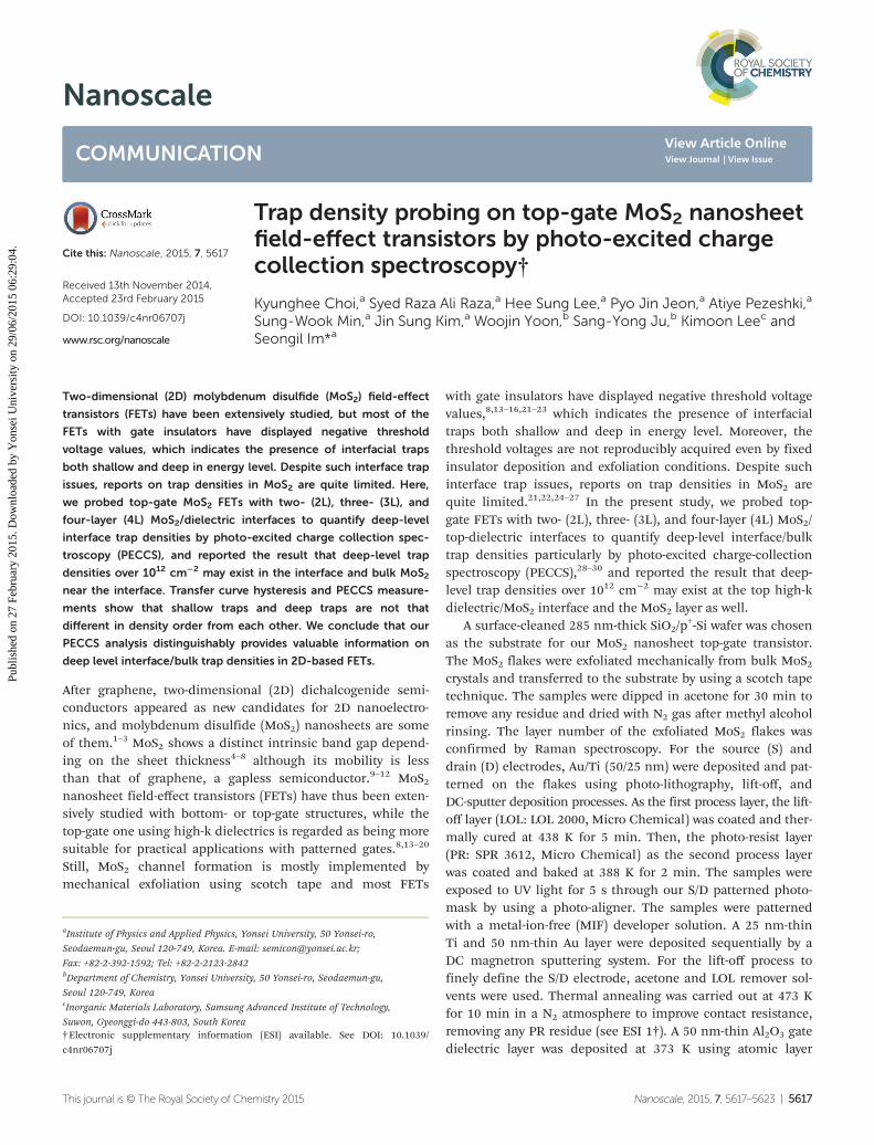
Fig. 2a, b, and c display the drain current–gate voltage(ID–VG) transfer characteristics of the 2L, 3L, and 4L MoS2nanosheet transistors, respectively. According to the draincurrent–drain voltage (ID–VD) output characteristics at variousVG values shown in Fig. 2d, e and f, the Au/Ti S/D contacts arequite ohmic for all FETs, although some contact resistancewould be expected from the FET with the 2L nanosheet. Theon/off current ratio of all transistors is ∼106 with a high on-current of a few μA (the gate leakage current, IG, is also shownto be a few pA). The linear mobilities (μlin) are respectively esti-mated to be 3.1, 1.4, and 2.1 cm2 V−1 s−1 as the maximumvalues for the 2L, 3L, and 4L MoS2 transistors, when they areplotted as a function of VG (shown in the respective insets).
Fig. 1 Optical microscopy (OM) images of the (a) two-layer (2L), (b) three-layer (3L), and (c) four-layer (4L) MoS2-based top-gate transistor on topof a silicon substrate with 285 nm-thick SiO2. Each inset photograph shows a magnified image of the Au/Ti source/drain electrodes and the ex-foliated MoS2 before patterning of the ITO top-gate electrode. (d) Raman spectra of the 2L, 3L, and 4L MoS2 flakes with the inset showing the atomicdisplacement of the two representative Raman-active modes: E12g and A1g. (e) Three-dimensional schematic view of a top-gate transistor with asingle-layered MoS2 nanosheet, an Al2O3 dielectric layer and ITO as a top-gate electrode under monochromatic light for the photo-excited charge-collection spectroscopy (PECCS) measurements. (The transmittance of the light was more than 80% after passing through the Al2O3 and ITO,ESI 2†).
Communication Nanoscale
5618 | Nanoscale, 2015, 7, 5617–5623 This journal is © The Royal Society of Chemistry 2015
Publ
ishe
d on
27
Febr
uary
201
5. D
ownl
oade
d by
Yon
sei U
nive
rsity
on
29/0
6/20
15 0
6:29
:04.
View Article Online
The mobility was estimated using the following well-knownequation:13,15
μlin ¼ @ID@VG
1CoxVD W=Lð Þ ð1Þ
where Cox is the dielectric capacitance per unit area.All the transistors show a large negative threshold voltage
(VTh) of −12∼−18 V. In classical reasoning, this might be dueto the positive fixed charges introduced during the ALDprocess in the Al2O3 dielectric layer or at the MoS2 channel/Al2O3 dielectric interface.22,24 The positive charge generates anegative shift in the flat-band voltage (VFB) (that would contrib-ute to the same amount of VTh shift) where VFB is describedbelow:32
VFB ¼ ΦMS � Qf
Cox� 1Cox
ðxox0
xxox
ρ xð Þdx ð2Þ
where ΦMS is the metal–semiconductor work-function differ-ence, Qf is the fixed trap charge per unit area near thechannel/dielectric interface, ρ(x) is the charge density of thebulk traps in the gate dielectric, and xox is the dielectric thick-ness. However, if the ALD process also introduced suchcharges into the MoS2 channel as dopants and impuritiesmaking the channel more conductive, the flat band voltageequation, eqn (2), should be modified and the thresholdvoltage equation should also be modified, to result in muchmore negative values. In fact, we have several evidences for the
ALD-induced doping effects in ESI 3.† In all the ALD dielec-trics, such doping effects are quite apparent. Although suchthreshold voltage modifications might be too complex to beconsidered here, we could properly modify eqn (2) for the VFBby newly defining Qf as below, since our channels are only afew nm thin:
Qf ¼ Qit þ Qbt ¼ Qit þ qNbtt ð3Þwhere Qit is the trap charge per unit area at the interface andQbt is for the near-interface bulk trap charges which can bedescribed as qNbtt, while q is an electronic charge, Nbt is thevolume density of the bulk traps near the interface and t is theMoS2 thickness.
The transfer curves show a hysteresis, which was heredefined as the variation of VTh (ΔVTh) at ID = 1 nA when VG isswept from −20 V to 20 V (forward) and then swept back(reverse) to −20 V. The hysteresis values for 2L, 3L, and 4L areestimated to be 2.45, 1.60, and 3.15 V, respectively. This isprobably due to the shallow level positive charges located atthe MoS2/Al2O3 interface which can trap/detrap electronsduring the forward/reverse VG sweep. The amount of trapcharge density is approximately estimated to be 1.92 × 1012,1.26 × 1012, and 2.47 × 10¹² q cm−2 for the 2L, 3L, and 4L MoS2transistors using the following equation and also assumingthat the trap charge density at the dielectric/semiconductorinterface is only influential and those in the dielectric oxideare mostly not:
ΔQ ¼ ΔVThCox ð4ÞThis estimation does not give any energy level information
of the deep traps, stemming only from the charges shallowenough to be trapped/detrapped under the gate bias sweep.According to the hysteresis direction (clockwise), the trappedcharges are regarded as electrons. There are a few papersregarding hysteresis in top-gated MoS2 transistors, but still thenature of this has not been fully understood.21,33,34
As a more general approach for the near-interface trap ana-lysis, the subthreshold swing (SS) was measured from thesame transfer curves: the SS values were 0.39, 0.44, and 0.50 Vdec−1 for the 2L, 3L, and 4L MoS2 transistors, respectively,when obtained using (d log(ID)/dVG)
−1 in an ID range from10 to 100 pA. The SS of the transistor is related to the interfacetrap density (Dit) i.e. the average density of state (DOS) for thedielectric/semiconductor interface traps, and the bulk trapdensity (Nbt) i.e. the DOS for the bulk of the semiconductornear the interface, based on the following equation:23
SS ¼ lnð 10Þ kTq
� �1þ q
Cox
ffiffiffiffiffiffiffiffiffiffiffiffiffiεchNbt
kT
rþ qDit
!" #ð5Þ
where kT = 0.026 eV at room temperature and εch is the dielec-tric constant of a 2D or thin-film semiconductor. Using the SSvalues and by setting Nbt = 0, the maximum Dit values are esti-mated to be 4.33 × 10¹², 5.00 × 10¹², and 5.78 × 1012 cm−2 eV−1
for the 2L, 3L, and 4L MoS2 transistors respectively, and itshould be noted that this average Dit may include the densities
Fig. 2 Drain current–gate voltage (ID–VG) transfer curves of the top-gate transistors with (a) 2L, (b) 3L, and (c) 4L MoS2 as obtained at VD =0.5 V. IG indicates the gate leakage current. Drain current–drain voltage(ID–VD) output curves of the (d) 2L, (e) 3L, and (f ) 4L MoS2-based transis-tors with a VG sweep from −20 V to +20 V (9 steps). The respective insetcurve shows the VG-dependent linear mobility plots.
Nanoscale Communication
This journal is © The Royal Society of Chemistry 2015 Nanoscale, 2015, 7, 5617–5623 | 5619
Publ
ishe
d on
27
Febr
uary
201
5. D
ownl
oade
d by
Yon
sei U
nive
rsity
on
29/0
6/20
15 0
6:29
:04.
View Article Online

from both the shallow and deep level traps (both at the inter-face and the semiconductor bulk near the interface). Thedifference between the Dit values among 2L, 3L, and 4L is mar-ginal but still worth considering. This difference could beunderstandable because in the common sense the thickernanoflakes (4L) might have more interlayers (as trapping sites)than the thinner (2L or 3L) ones. The higher trap density esti-mated by SS than by hysteresis is also understandable, sincethe SS-driven value reflects both the shallow and deep traps indensity while the hysteresis reflects only the shallow ones.
Our top-gate MoS2 transistors were also subjected to posi-tive bias stress (PBS) under the conditions VG = 20 V and VD =0.5 V while the stress was stopped at approximately logarith-mic time intervals to measure the transfer curves of our tran-sistors. Fig. 3a, b, and c show the final states of the transfercharacteristics of the 2L, 3L, and 4L MoS2 transistors after3600 s, respectively as overlaid on their initial states. Accordingto the figures, the curves gradually moved to the positive sidebut by only a small amount of ΔVTh without much SS or hyster-esis change. The shift was so minimal that the PBS-driven trapcharge density with electrons might be estimated to be lessthan 5 × 10¹¹ q cm−2 from the ΔVThCox calculation in eqn (4).These results may indicate that both the 2D channel surfaceand the dielectric oxide in our top-gate MoS2 transistors aresurprisingly strong and resistant against electrical stress,although they surely have ALD-induced charges inside.Charges inside the dielectric turned out not to be influentialto the hysteresis under gate stress and sweep as we assumed inprevious paragraphs for Fig. 2. [Such bias stress resistance washardly shown in the single-crystalline ZnO nanowire-basedFETs with ALD Al2O3 dielectric, indicating that the MoS2surface is much more flawless than that of the ZnO nanowire.(ESI 4†)]
We have discussed so far the shallow trap charge densityestimated by hysteresis and the average density of state, Dit,which is summed and averaged over the whole sub band gaprange. Here we also probed the deep trap charges near theinterface with a quantification method, PECCS measurements,
for the 2L, 3L, and 4L MoS2 transistors.28–30 As a first step,photo-induced transfer curves were measured sequentially byapplying monochromatic photons in the wavelength rangefrom 1800 nm (0.69 eV) to 600 nm (2.07 eV) with an interval of5 nm. The VG sweep started from the channel accumulation tothe depletion state because we should initially fill up all theinterface trap states with charge carriers prior to every photo-excitation. When photons with a certain energy (ε) illuminatethe region near the channel/dielectric interface, most of thetrap charges (electrons) trapped in the gap states between theconduction band minimum (CBM) and the CBM-ε are excitedto the CBM level. Hence the initial fixed charge Qf near theinterface is varied to Qeff(ε), which is mainly for the trapsremaining at and near the channel/dielectric interface. Thelight-induced effective trap charge modulation (ΔQeff(ε)) isacquired by the shift of VFB (ΔVFB(ε)) which is the differencebetween the photo-induced VFB and the initial VFB. Therelationship can be expressed as follows:28–30
ΔVFB εð Þ ¼ � ΔQeff εð ÞCox
where
ΔQeffðεÞ ¼ Qf � QeffðεÞ ð6Þ
Qeff εð Þ ¼ qðCBM�ε
VBMDit εð Þdε ð7Þ
where CBM and VBM are the conduction band minimum andthe valence band maximum, respectively. Then, Dit has arelationship with VFB:
Dit CBM� εð Þ ¼ �Cox
q@VFB εð Þ
@εð8Þ
Fig. 4a, b, and c show the transfer curves of the 2L, 3L, and4L MoS2 transistors under several monochromatic photonsalong with the dark transfer curve. Based on the series ofphoto-induced transfer characteristics of the transistors at afixed VD = 0.5 V, we estimated the photo-induced negativeΔVFB(ε) and calculated ΔQeff(ε) with respect to the photonenergy (ε), using eqn (6). Fig. 4d shows the |ΔQeff(ε)| plot as afunction of ε for the 2L, 3L, and 4L MoS2 transistors. The deeptrap charge density monotonously increases without showingany rapid increase in intensity until the photon energy reachesthe band edge (starting at 0.69 eV). Moreover, such monoto-nous increase was more obvious with the thicker MoS2. Theseresults suggest two strong probabilities in our measurement:(1) most of the deep traps broadly exist above a level of CBM =0.69 eV, located near the top-gate interface (which means boththe interface and the 2–4L thin bulk). There have been somereports about theoretical predictions of deep states like asulfur vacancy with an energy level 0.4–0.6 eV below theCBM,35–37 which our light source for the PECCS measurementscannot provide due to its own lowest photon energy limit at0.69 eV. The detailed nature of such dopant and trap impuri-ties near the interface is not identified yet, and will be dis-cussed in a future study along with the ALD-induced doping. (2)
Fig. 3 Transfer curves of the (a) 2L, (b) 3L, and (c) 4L MoS2-based tran-sistors after 3600 s period positive gate bias stress (PBS) under VG = 20V and VD = 0.5 V, as overlaid on their respective initial transfer curves.
Communication Nanoscale
5620 | Nanoscale, 2015, 7, 5617–5623 This journal is © The Royal Society of Chemistry 2015
Publ
ishe
d on
27
Febr
uary
201
5. D
ownl
oade
d by
Yon
sei U
nive
rsity
on
29/0
6/20
15 0
6:29
:04.
View Article Online

Our eqn (3) is consistent with our PECCS data, where|ΔQeff(ε)| increases monotonously with the thickness, becauseQit should be the same regardless of thickness but Qbt
(= qNbtt ) should increase with the thickness or layer number.On the one hand, a somewhat rapid increase of |ΔQeff(ε)|
appears to start near 1.54 eV for 2L, 1.42 eV for 3L, and 1.33 eVfor 4L as indicated by the arrows, whose values are consistentwith the previously reported indirect band-to-band transitionof MoS2 nanosheets.7,8 Therefore, according to the plots, thedensity values for the sub band gap trap charge (Qf ormaximum ΔQeff ) are now estimated to be ∼1.00 × 10¹², 1.15 ×10¹², and 1.37 × 10¹² q cm−2 for the 2L, 3L, and 4L transistors,respectively. [So, we could actually separate the average Qit andNbt values as 0.7 × 10¹² q cm−2 and 2.8 × 1018 cm−3, respect-ively, based on the t-dependent |ΔQeff(ε)| plots from the 2L,3L, and 4L MoS2 transistors (see ESI 5† for more details).]These deep trap charge densities are not higher than theshallow trap charge densities estimated by hysteresis. Thesums of the deep and shallow trap densities appear to be∼2.92 × 10¹², ∼2.41 × 10¹², and ∼3.84 × 1012 cm−2 for the 2L,3L, and 4L transistors, respectively. These sums are smallerthan those estimated by SS, since the SS-driven average
Dit × energy gaps (1.54, 1.42, and 1.33 eV for 2L, 3L, and 4LMoS2) work out to be 6.67 × 10¹², 7.10 × 10¹² and 7.69 × 10¹²
cm−2 for the 2L, 3L, and 4L transistors, respectively. Thisdifference in the sum may be attributed to the limit of the SSequation (eqn (5)) which reflects any influence by contactresistance. However, the values from SS and hysteresis/PECCSare of the same order of magnitude and are comparable toeach other. The trap density values estimated from the SS, hys-teresis, and PECCS measurements are summarized in Table 1for a more detailed comparison.
As a by-product, the PECCS-driven Dit plot is shown in theinset of Fig. 4d, where a Dit peak intensity of about 4.0 × 10¹²
cm−2 eV−1 is displayed near the band edges (onset region:1.54, 1.42, and 1.33 eV) for the 2L, 3L, and 4L transistors,while the direct band-to-band transition of MoS2 i.e. thesecond band gap is also observed with a large threshold shiftin the photo-induced transfer curves at 1.80 eV for both tran-sistors as shown in Fig. 4a, b, and c. We thus regard ourPECCS measurements as providing quite valuable informationin both respects: the near-interface trap density of the MoS2FETs and the indirect/direct optical gap of the 2D MoS2.
As a final brief concern, we have considered extracting outthe contact resistance-exempted linear mobilities of the 2L, 3L,and 4L MoS2 FETs from their respective transfer and outputcurves in Fig. 2 (see ESI 6† for the detailed extractionmethods38), since their field mobility values appear to be quitesmaller than the generally reported ones; such small mobili-ties would be mainly due to coulomb and surface roughnessscatterings by ALD-induced impurities and pin-holes,39–41 butpartially because of large contact resistances. As a result, 19.4,1.44, and 1.7 cm2 V−1 s−1 were respectively achieved as contactresistance-free mobilities from the 2L, 3L, and 4L MoS2 FETs,which had field mobilities of 3.1, 1.4, and 2.1 cm2 V−1 s−1. The7 times-enhanced mobility of the 2L MoS2 indicates that it hasa higher Schottky barrier and contact resistance due to itslarger band gap than those of the thicker MoS2 channels.
Conclusions
In summary, we have fabricated top-gate 2D MoS2 FETs for 2L-, 3L-, and 4L-thin channels with ITO gate electrodes, to probethe shallow and deep level traps located at or near the dielec-tric ALD-grown Al2O3/MoS2 interface. Transfer curve hysteresis
Fig. 4 Photo-induced transfer curves of the (a) 2L, (b) 3L, and (c) 4LMoS2-based transistors under monochromatic light of various wave-lengths for the PECCS measurements. (d) Photon energy-dependenteffective trap charge modulation (ΔQeff ) plots for the 2L, 3L, and 4LMoS2-based transistors. The black dotted lines with arrows indicate theindirect band gap transition regions and the total ΔQeff values within thesub band gap region for the 2L, 3L, and 4L MoS2 whereas the insetshows the density of states (Dit) profile that may indicate the onset ofthe first indirect gap (1.54, 1.42, and 1.33 eV respectively for 2L, 3L, and4L) and the second direct gap energy (1.80 eV).
Table 1 Summary of the hysteresis, PECCS, and SS estimated trapdensities
Number ofMoS2 layers
Trap density (×1012 cm−2) obtained from
Hysteresis PECCSHysteresis& PECCS SS
2 1.92 1.00 2.92 6.673 1.26 1.15 2.41 7.104 2.47 1.37 3.84 7.69
Nanoscale Communication
This journal is © The Royal Society of Chemistry 2015 Nanoscale, 2015, 7, 5617–5623 | 5621
Publ
ishe
d on
27
Febr
uary
201
5. D
ownl
oade
d by
Yon
sei U
nive
rsity
on
29/0
6/20
15 0
6:29
:04.
View Article Online
and PECCS measurements show that the shallow traps and thedeep traps are not much different in density order from eachother. The total trap density estimated by SS, and PECCS andhysteresis displayed about the same order as a few number×1012 cm−2 for both cases, however the SS-driven trap densityalways appears relatively higher because it can not exclude theinfluence of contact resistance. The PECCS analysis directlydistinguishes the near-interface deep traps unlike othermethods,21,22,24–27 even separating the interface trap charge(Qit) and the near-interface bulk traps (Qbt/or Nbt). We thusconclude that our PECCS analysis provides valuable infor-mation on the deep level near-interface trap density of top-gatefew layer MoS2 FETs.
Acknowledgements
The authors acknowledge the financial support from NRF(NRL program: grant no. 2014R1A2A1A01004815), Nano-Materials Technology Development Program (grant no.2012M3A7B4034985) and Brain Korea 21 plus Program.
Notes and references
1 J. N. Coleman, M. Lotya, A. O’Neill, S. D. Bergin, P. J. King,U. Khan, K. Young, A. Gaucher, S. De, R. J. Smith,I. V. Shvets, S. K. Arora, G. Stanton, H. Kim, K. Lee,G. T. Kim, G. S. Duesberg, T. Hallam, J. J. Boland,J. J. Wang, J. F. Donegan, J. C. Grunlan, G. Moriarty,A. Shmeliov, R. J. Nicholls, J. M. Perkins, E. M. Grieveson,K. Theuwissen, D. W. McComb, P. D. Nellist andV. Nicolosi, Science, 2011, 331, 568.
2 Q. H. Wang, K. Kalantar-Zadeh, A. Kis, J. N. Coleman andM. S. Strano, Nat. Nanotechnol., 2012, 7, 699.
3 M. Chhowalla, H. S. Shin, G. Eda, L. Li, K. P. Loh andH. Zhang, Nat. Chem., 2013, 5, 263.
4 T. Li and G. Galli, J. Phys. Chem., 2007, 111, 16192.5 A. Kuc, N. Zibouche and T. Heine, Phys. Rev. B: Condens.
Matter, 2011, 83, 245213.6 A. Splendiani, L. Sun, Y. Zhang, T. Li, J. Kim, C. Chim,
G. Galli and F. Wang, Nano Lett., 2010, 10, 1271.7 K. F. Mak, C. Lee, J. Hone, J. Shan and T. F. Heinz, Phys.
Rev. Lett., 2010, 105, 136805.8 H. S. Lee, S. Min, Y. Chang, M. K. Park, T. Nam, H. Kim,
J. H. Kim, S. Ryu and S. Im, Nano Lett., 2012, 12, 3695.9 A. K. Geim, Science, 2009, 324, 1530.10 K. S. Novoselov, D. Jiang, F. Schedin, T. J. Booth,
V. V. Khotkevich, S. V. Morozov and A. K. Geim, Proc. Natl.Acad. Sci. U. S. A., 2005, 102, 10451.
11 I. Meric, M. Y. Han, A. F. Young, B. Ozyilmaz, P. Kim andK. L. Shepard, Nat. Nanotechnol., 2008, 3, 654.
12 X. Du, I. Skachko, A. Barker and E. Y. Andrei, Nat. Nano-technol., 2008, 3, 491.
13 B. Radisavljevic, A. Radenovic, J. Brivio, V. Giacometti andA. Kis, Nat. Nanotechnol., 2011, 6, 147.
14 S. Kim, A. Konar, W. Hwang, J. H. Lee, J. Lee, J. Yang,C. Jung, H. Kim, J. Yoo, J. Choi, Y. W. Jin, S. Y. Lee, D. Jena,W. Choi and K. Kim, Nat. Commun., 2012, 3, 1011.
15 H. Li, Z. Yin, Q. He, H. Li, X. Huang, G. Lu, D. W. H. Fam,A. I. Y. Tok, Q. Zhang and H. Zhang, Small, 2012, 8, 63.
16 B. Radisavljevic, M. B. Whitwick and A. Kis, ACS Nano,2011, 5, 9934.
17 K. Choi, Y. T. Lee, S. Min, H. S. Lee, T. Nam, H. Kim andS. Im, J. Mater. Chem. C, 2013, 1, 7803.
18 O. Lopez-Sanchez, D. Lembke, M. Kayci, A. Radenovic andA. Kis, Nat. Nanotechnol., 2013, 8, 497.
19 H. Wang, L. Yu, Y. Lee, Y. Shi, A. Hsu, M. L. Chin, L. Li,M. Dubey, J. Kong and T. Palacios, Nano Lett., 2012, 12,4674.
20 H. S. Lee, S. Min, M. K. Park, Y. T. Lee, P. J. Jeon, J. H. Kim,S. Ryu and S. Im, Small, 2012, 8, 3111.
21 X. Zou, J. Wang, C. Chiu, X. Xiao, C. Jiang, W. Wu, L. Mai,T. Chen, J. Li, J. C. Ho and L. Liao, Adv. Mater., 2014, 26,6255.
22 H. Liu and P. D. Ye, IEEE Electron Device Lett., 2012, 33,546.
23 S. Min, H. S. Lee, H. J. Choi, M. K. Park, T. Nam, H. Kim,S. Ryu and S. Im, Nanoscale, 2013, 5, 548.
24 J. Na, M. Joo, M. Shin, J. Huh, J. Kim, M. Piao, J. Jin,H. J. Choi, J. H. Shin and G. Kim, Nanoscale, 2014, 6, 433.
25 J. Renteria, R. Samnakay, S. L. Rumyantsev, C. Jiang,P. Goli, M. S. Shur and A. A. Balandin, Appl. Phys. Lett.,2014, 104, 153104.
26 S. Ghatak and A. Ghosh, Appl. Phys. Lett., 2013, 103,122103.
27 S. Ghatak and A. Ghosh, http://arxiv.org/abs/1403.3333, 2014.28 K. Lee, M. S. Oh, S. Mun, K. H. Lee, T. W. Ha, J. H. Kim,
S. K. Park, C. Hwang, B. H. Lee, M. M. Sung and S. Im, Adv.Mater., 2010, 22, 3260.
29 K. Lee, G. Ko, G. H. Lee, G. B. Han, M. M. Sung, T. W. Ha,J. H. Kim and S. Im, Appl. Phys. Lett., 2010, 97, 082110.
30 S. Im, Y. Chang and J. H. Kim, Photo-Excited Charge Collec-tion Spectroscopy: Probing the Traps in Field-Effect Transistor,Springer, New York, 2013.
31 C. Lee, H. Yan, L. E. Brus, T. F. Heinz, J. Hone and S. Ryu,ACS Nano, 2010, 4, 2695.
32 R. S. Muller, T. I. Kamins and M. Chan, Device Electronicsfor Integrated Circuits, Wiley, New York, 2003.
33 Y. Zhang, J. Ye, Y. Matsuhashi and Y. Iwasa, Nano Lett.,2012, 12, 1136.
34 M. M. Perera, M. Lin, H. Chuang, B. P. Chamlagain,C. Wang, X. Tan, M. M. Cheng, D. Tománek and Z. Zhou,ACS Nano, 2013, 7, 4449.
35 H. Qiu, T. Xu, Z. Wang, W. Ren, H. Nam, Z. Ni, Q. Chen,S. Yuan, F. Miao, F. Song, G. Long, Y. Shi, L. Sun, J. Wangand X. Wang, Nat. Commun., 2013, 4, 2642.
36 D. Liu, Y. Guo, L. Fang and J. Robertson, Appl. Phys. Lett.,2013, 103, 183113.
37 W. Zhou, X. Zou, S. Najmaei, Z. Liu, Y. Shi, J. Kong, J. Lou,P. M. Ajayan, B. I. Yakobson and J. Idrobo, Nano Lett., 2013,13, 2615.
Communication Nanoscale
5622 | Nanoscale, 2015, 7, 5617–5623 This journal is © The Royal Society of Chemistry 2015
Publ
ishe
d on
27
Febr
uary
201
5. D
ownl
oade
d by
Yon
sei U
nive
rsity
on
29/0
6/20
15 0
6:29
:04.
View Article Online

38 G. Horowitz, R. Hajlaoui, D. Fichou and A. E. Kassmi, Appl.Phys. Lett., 1999, 85, 3202.
39 A. Azcatl, S. McDonnell, S. K. C, X. Peng, H. Dong, X. Qin,R. Addou, G. I. Mordi, N. Lu, J. Kim, M. J. Kim, K. Cho andR. M. Wallace, Appl. Phys. Lett., 2014, 104, 111601.
40 J. Yang, S. Kim, W. Choi, S. H. Park, Y. Jung, M. Cho andH. Kim, ACS Appl. Mater. Interfaces, 2013, 5, 4739.
41 S. McDonnell, B. Brennan, A. Azcatl, N. Lu, H. Dong,C. Buie, J. Kim, C. L. Hinkle, M. J. Kim and R. M. Wallace,ACS Nano, 2013, 7, 10354.
Nanoscale Communication
This journal is © The Royal Society of Chemistry 2015 Nanoscale, 2015, 7, 5617–5623 | 5623
Publ
ishe
d on
27
Febr
uary
201
5. D
ownl
oade
d by
Yon
sei U
nive
rsity
on
29/0
6/20
15 0
6:29
:04.
View Article Online


![Capacitance behaviors of Polyaniline/Graphene Nanosheet ...carbonlett.org/Upload/files/CARBONLETT/[51-54]-01.pdf · Capacitance behaviors of Polyaniline/Graphene Nanosheet Composites](https://static.fdocuments.us/doc/165x107/5e22180dfe8b0d23b379e7f6/capacitance-behaviors-of-polyanilinegraphene-nanosheet-51-54-01pdf-capacitance.jpg)


