
Transmission line model - Dr. Montoya's Webpage- Spring...
16
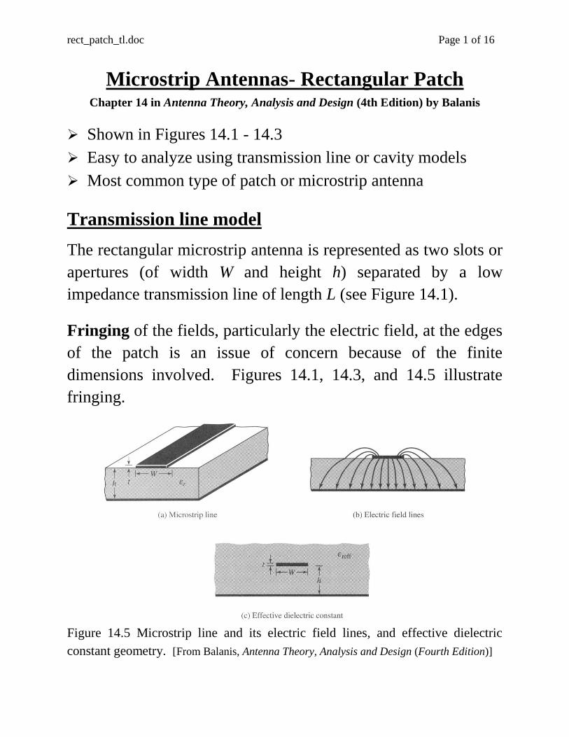
rect_patch_tl.doc Page 1 of 16 Microstrip Antennas- Rectangular Patch Chapter 14 in Antenna Theory, Analysis and Design (4th Edition) by Balanis Shown in Figures 14.1 - 14.3 Easy to analyze using transmission line or cavity models Most common type of patch or microstrip antenna Transmission line model The rectangular microstrip antenna is represented as two slots or apertures (of width W and height h) separated by a low impedance transmission line of length L (see Figure 14.1). Fringing of the fields, particularly the electric field, at the edges of the patch is an issue of concern because of the finite dimensions involved. Figures 14.1, 14.3, and 14.5 illustrate fringing. Figure 14.5 Microstrip line and its electric field lines, and effective dielectric constant geometry. [From Balanis, Antenna Theory, Analysis and Design (Fourth Edition)]
Transcript of Transmission line model - Dr. Montoya's Webpage- Spring...
rect_patch_tl.doc Page 1 of 16
Microstrip Antennas- Rectangular Patch Chapter 14 in Antenna Theory, Analysis and Design (4th Edition) by Balanis
Shown in Figures 14.1 - 14.3
Easy to analyze using transmission line or cavity models
Most common type of patch or microstrip antenna
Transmission line model
The rectangular microstrip antenna is represented as two slots or
apertures (of width W and height h) separated by a low
impedance transmission line of length L (see Figure 14.1).
Fringing of the fields, particularly the electric field, at the edges
of the patch is an issue of concern because of the finite
dimensions involved. Figures 14.1, 14.3, and 14.5 illustrate
fringing.
Figure 14.5 Microstrip line and its electric field lines, and effective dielectric
constant geometry. [From Balanis, Antenna Theory, Analysis and Design (Fourth Edition)]

rect_patch_tl.doc Page 2 of 16
Fringing makes the patch seem bigger (electrically) than the
physical dimensions of the patch. This impacts the resonant
frequency of the patch. It is dependent on the dielectric constant
r of the substrate as well as the physical dimensions L, W and h.
To account for the fringing of the electric field above the
microstrip (in the air above the substrate), an effective dielectric
constant 1< r,eff < r is defined. As most of the field lines are
confined between the patch and the ground plane (like a
capacitor), r,eff tends to be closer to r. The effective dielectric
constant allows the microstrip to be modeled as if it were in a
homogeneous dielectric medium of r,eff. Figure 14.6 shows the
effective dielectric constant as a function of frequency for
several substrates. Note that r,eff → r as the frequency
increases, i.e., the electric field concentrates in the substrate.
Figure 14.6 Effective dielectric constant versus frequency for typical substrates.
[From Balanis, Antenna Theory, Analysis and Design (Fourth Edition)]
rect_patch_tl.doc Page 3 of 16
The initial (low frequency) value of r,eff is 0.5
r,eff
1 11 12
2 2
r r h
W
where W/h > 1.
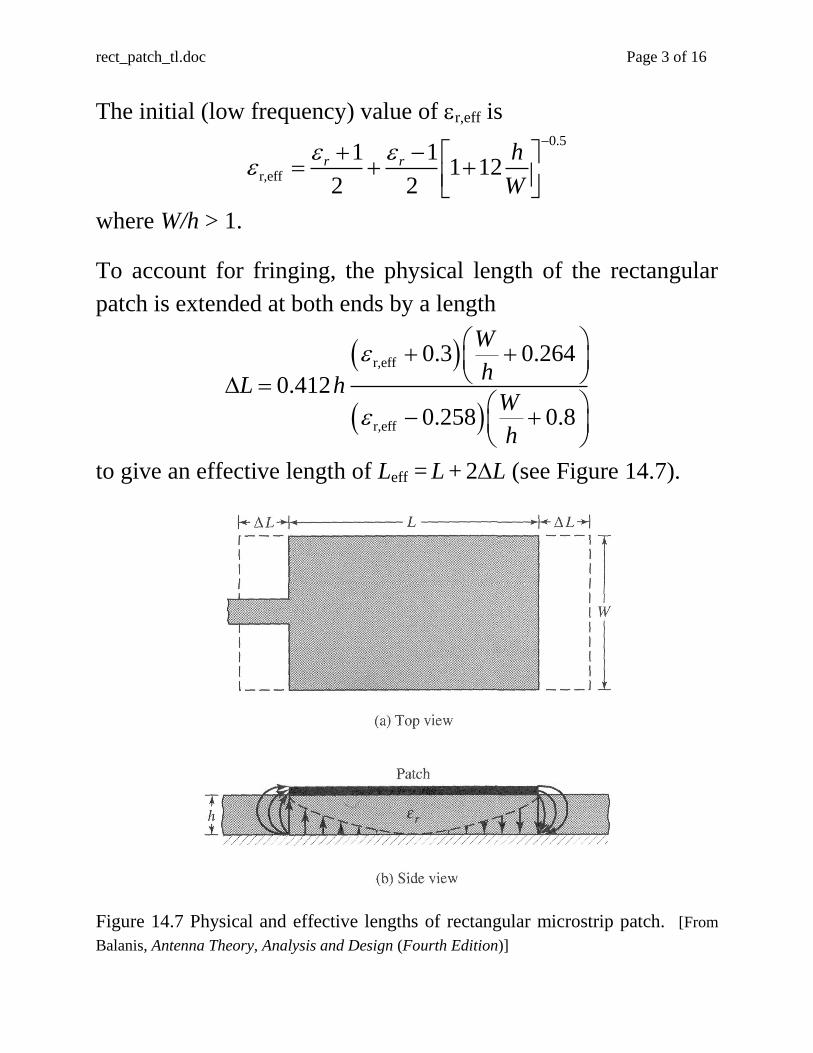
To account for fringing, the physical length of the rectangular
patch is extended at both ends by a length
r,eff
r,eff
0.3 0.264
0.412
0.258 0.8
W
hL h
W
h
to give an effective length of Leff = L + 2L (see Figure 14.7).
Figure 14.7 Physical and effective lengths of rectangular microstrip patch. [From
Balanis, Antenna Theory, Analysis and Design (Fourth Edition)]

rect_patch_tl.doc Page 4 of 16
For the dominant TM010 mode (patch acts as a cavity resonator),
the resonant frequency is
010
(uncorrected)2
r
r
cf
L
,c 010eff r,eff
(corrected)2
=2
r
r
cf
L
cq
L
where q is the fringing factor
,c 010
010
r
r
fq
f
Solving for Leff, we get
eff
,c r,eff01022 r
cL
f
where is the guided wavelength (Note: want (fr,c)010 = fr ).
Now, we can return to the transmission line model where we
will represent the two radiating slots with parallel equivalent
admittances
1 1 1
2 2 2
Slot #1
Slot #2
Y G j B
Y G j B
separated by a microstrip transmission line of length L with

rect_patch_tl.doc Page 5 of 16
characteristic admittance Yc =
1/Zc (see Figure 14.9). Moreover,
for rectangular patches, the slots are identical
1 2 1 2 1 2 and Y Y G G B B
Figure 14.9 Rectangular microstrip patch and its equivalent circuit transmission
model. [From Balanis, Antenna Theory, Analysis and Design (Fourth Edition)]
How can we calculate the slot admittances? A simple derivation
(based on infinitely long slots) that assumes that the electric
field is uniform across the slot(s) yields
2
1 0
0 0
1 0
0 0
1 11 for
120 24 10
11 0.636ln for
120 10
W hG k h
W hB k h
where 0
0
2k
c
is the free space wave number. This result
is accurate only when W >> 0 and h << 0.
rect_patch_tl.doc Page 6 of 16
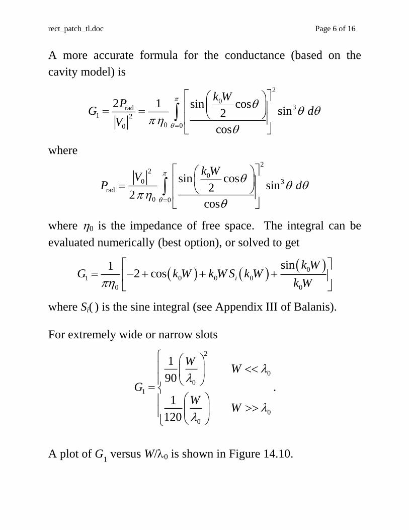
A more accurate formula for the conductance (based on the
cavity model) is
2
03rad
1 2
0 00
2 1 sin cossin2
cos
k WP
G dV
where 2
20
0 3
rad
0 0
sin cossin2
2cos
k WV
P d
where 0 is the impedance of free space. The integral can be
evaluated numerically (best option), or solved to get
0
1 0 0 0
0 0
sin12 cos i
k WG k W k W S k W
k W
where Si( ) is the sine integral (see Appendix III of Balanis).
For extremely wide or narrow slots
2
0
0
1
0
0
1
90
1
120
WW
GW
W
.
A plot of G1 versus W/0 is shown in Figure 14.10.

rect_patch_tl.doc Page 7 of 16
Figure 14.10 Slot conductance as a function of slot width. [From Balanis, Antenna
Theory, Analysis and Design (Fourth Edition)]
To get the input admittance Yin, the admittance of slot #2 (Y2)
must be translated across the length of the rectangular patch to
the location of slot #1 and added to Y1 (they are in parallel). If
this length (somewhere between Leff and L < /2) is properly
selected, the translated slot #2 admittance is
*
2 2 2 1 1 1Y G jB G jB Y .
Then, the input admittance and impedance become
in 1 2 12Y Y Y G
and
in in
in 1
1 1
2Z R
Y G .
rect_patch_tl.doc Page 8 of 16
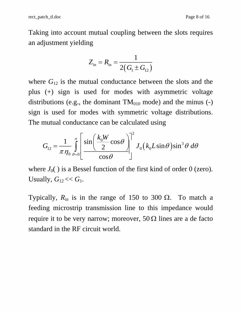
Taking into account mutual coupling between the slots requires
an adjustment yielding
in in
1 12
1
2Z R
G G
where G12 is the mutual conductance between the slots and the
plus (+) sign is used for modes with asymmetric voltage
distributions (e.g., the dominant TM010 mode) and the minus (-)
sign is used for modes with symmetric voltage distributions.
The mutual conductance can be calculated using
2
03
12 0 0
0 0
1 sin cossin sin2
cos
k W
G J k L d
where J0( ) is a Bessel function of the first kind of order 0 (zero).
Usually, G12 << G1.
Typically, Rin is in the range of 150 to 300 . To match a
feeding microstrip transmission line to this impedance would
require it to be very narrow; moreover, 50 lines are a de facto
standard in the RF circuit world.

rect_patch_tl.doc Page 9 of 16
Therefore, the question arises, “How can we adjust Rin?”
Rin can be decreased by increasing W. This action is limited
to W/L < 2 because the aperture efficiency of the slots drops
for W/L > 2.
An alternative is to use an inset or recessed microstrip feed
(see Figure 14.11). This works because the voltage is a
maximum and the current a minimum at the edges of the
patch, leading to large impedance values. As we go into the
patch, the voltage drops and the current increases, leading to
smaller impedances until we reach the midpoint of the patch.
The input resistance of the inset feed is given by
2 2
2 21 1 1in 0 0 0 02
1 12 ,feed,feed
1 2( ) cos sin sin
2 cc
G B BR y y y y
G G L L Y LY
where Yc,feed = 1/Zc,feed and Zc,feed is the characteristic impedance
of the feeding microstrip transmission line (width W0). Note:
the inset distance y0 must be in the range 0 < y0 < L/2.
The characteristic impedance Zc for any microstrip transmission
line of width W (i.e., the feed or patch) can be calculated using
r,eff
0
r,eff
60 8ln 1
4
1
1.393 0.667ln 1.444
c
h W W
W h h
Z W
hW W
h h
.
rect_patch_tl.doc Page 10 of 16
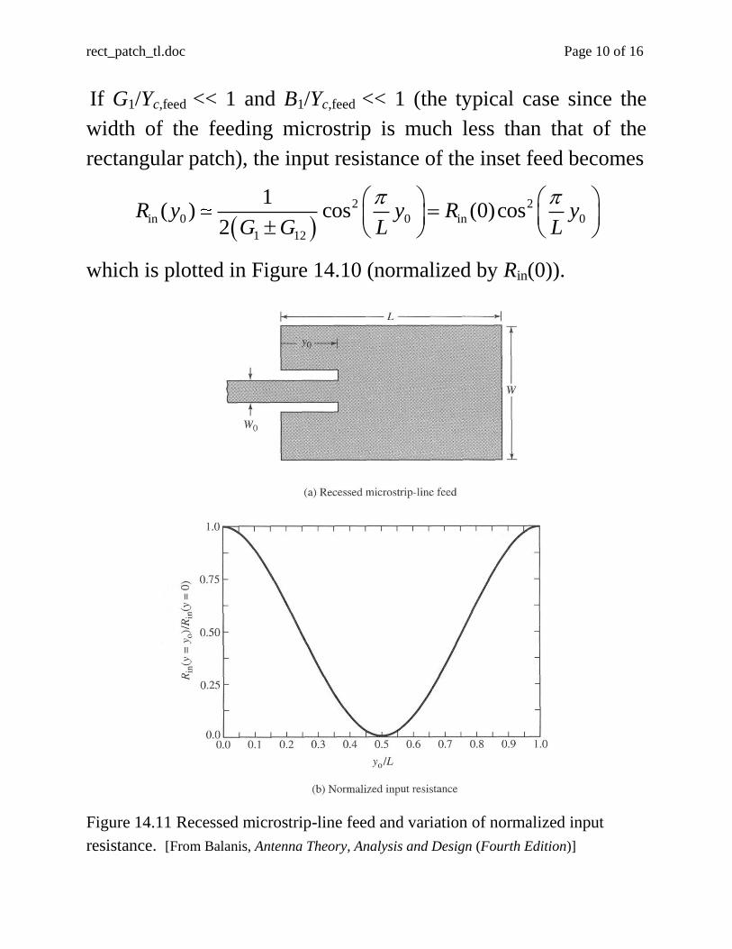
If G1/Yc,feed << 1 and B1/Yc,feed << 1 (the typical case since the
width of the feeding microstrip is much less than that of the
rectangular patch), the input resistance of the inset feed becomes
2 2
in 0 0 in 0
1 12
1( ) cos (0)cos
2R y y R y
G G L L
which is plotted in Figure 14.10 (normalized by Rin(0)).
Figure 14.11 Recessed microstrip-line feed and variation of normalized input
resistance. [From Balanis, Antenna Theory, Analysis and Design (Fourth Edition)]
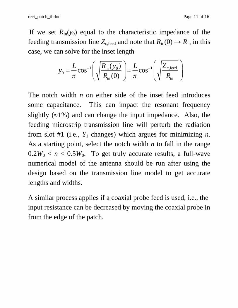
rect_patch_tl.doc Page 11 of 16
If we set Rin(y0) equal to the characteristic impedance of the
feeding transmission line Zc,feed and note that Rin(0) → Rin in this
case, we can solve for the inset length
,feed1 1in 0
0
in in
( )cos cos
(0)
cZL R y Ly
R R
The notch width n on either side of the inset feed introduces
some capacitance. This can impact the resonant frequency
slightly (1%) and can change the input impedance. Also, the
feeding microstrip transmission line will perturb the radiation
from slot #1 (i.e., Y1 changes) which argues for minimizing n.
As a starting point, select the notch width n to fall in the range
0.2W0 < n < 0.5W0. To get truly accurate results, a full-wave
numerical model of the antenna should be run after using the
design based on the transmission line model to get accurate
lengths and widths.
A similar process applies if a coaxial probe feed is used, i.e., the
input resistance can be decreased by moving the coaxial probe in
from the edge of the patch.
rect_patch_tl.doc Page 12 of 16
Design Procedure
1) Specify εr and h of substrate, the desired resonant frequency
fr , and the impedance Zc,feed of the feeding transmission line.
2) Calculate width of patch using
2
2 1r r
cW
f
(selected to give good radiation efficiency). Strictly, the
patch width should be less than the length (i.e., W < L) to
ensure operation only in the TM010 mode. Practically, W > L
can be used if the patch is excited/driven so as not to excite
other modes (e.g., TM001 mode is dominant when W > L). W
can be changed so long as W/L <
2, avoid aperture efficiency
decrease.
3) Calculate
0.5
r,eff
1 11 12
2 2
r r h
W
4) Calculate
r,eff
r,eff
0.3 0.264
0.412
0.258 0.8
W
hL h
W
h
5) Calculate the effective length and guided wavelength .
eff
r,eff2 r
cL
f
eff2L

rect_patch_tl.doc Page 13 of 16
6) Calculate the patch length L (see below) and L/. Then,
calculate and check that W/L < 2.
eff 2 22
L L L L
7) Calculate G1 G2 and B1
B2.
2
1,est 0
0 0
1,est 0
0 0
1 11 for
120 24 10
11 0.636ln for
120 10
W hG k h
W hB k h
2
03
1
0 0
1 sin cossin2
cos
k W
G d
11 1,est
1,est
GB B
G
where 0
0
2k
c
is the free space wave number.
8) Calculate the characteristic impedance Zc,ant and admittance
Yc,ant for the rectangular microstrip antenna.
r,eff
,ant 0
r,eff
60 8ln 1
4
1
1.393 0.667ln 1.444
c
h W W
W h h
Z W
hW W
h h

rect_patch_tl.doc Page 14 of 16
and
,ant
,ant
1c
c
YZ
9) (Optional) Use Smith chart or direct calculation to verify
*
2 2 2 1 1 1Y G jB G jB Y .
10) Calculate the mutual conductance between the slots
2
03
12 0 0
0 0
1 sin cossin sin2
cos
k W
G J k L d
11) Calculate Rin (used plus (+) sign in original equation).
in in
1 12
1
2Z R
G G
12) If an inset microstrip feed is required (i.e., Rin Zc,feed),
calculate length y0 of the inset needed to match the
rectangular patch to the feeding transmission line. When
G1/Yc,feed << 1 and B1/Yc,feed << 1,
,feed1
0
in
coscZL
yR
.
This answer can be checked using
2 2
2 20 0 01 1 1in 0 2
1 12 ,feed,feed
21( ) cos sin sin
2 cc
y y yG B BR y
G G L L Y LY
If Rin(y0) is not equal to Zc,feed, the length y0 should be
iteratively adjusted until Rin(y0) = Zc,feed.

rect_patch_tl.doc Page 15 of 16
13) Determine the width W0 of the feeding microstrip
transmission line.
Method 1:
If available, use information/tools from the manufacturer of
the substrate/PCB. For example, the Rogers Corporation
has an on-line JAVA calculator for determining the width
W0 of a microstrip transmission line based on desired Z0 and
the particular substrate at
http://www.rogerscorporation.com/mwu/mwi_java/Mwij_vp.html
Method 2:
Iteratively (i.e., guess a starting value of W0 < W ) determine
the width W0 of the feeding transmission line using 0.5
r,eff
0
1 11 12
2 2
r r h
W
and
0 0
0r,eff
,feed0 0
0 0r,eff
60 8ln 1
4
1
1.393 0.667ln 1.444
c
h W W
W h h
Z W
hW W
h h
.
Note that the effective permittivity must be recalculated for
the feeding transmission line because it has different
dimensions than the patch antenna (i.e., it is much
narrower).
rect_patch_tl.doc Page 16 of 16
Method 3:
Use the design equation
0
2
0
0
82
2
2 1 0.611 ln 2 1 ln( 1) 0.39 2
2
A
A
r
r r
We
e hW
WhB B B
h
.
where
,feed 1 1 0.110.23
60 2 1
c r r
r r
ZA
and
0
,feed2 c r
BZ
.
14) Select the notch width n in the range 0.2W0 < n < 0.5W0.
15) Draw resulting design.
W0
W
L
y0
Top View
n
n