Transmission-Line Essentials for Digital...
97
EM II / Prof. Tzong-Lin Wu 1 Transmission-Line Essentials for Digital Electronics Prof. Tzong-Lin Wu EMC Laboratory Department of Electrical Engineering National Taiwan University
Transcript of Transmission-Line Essentials for Digital...

EM II / Prof. Tzong-Lin Wu 1
Transmission-Line Essentials for Digital Electronics
Prof. Tzong-Lin Wu
EMC Laboratory
Department of Electrical Engineering
National Taiwan University
EM II / Prof. Tzong-Lin Wu 2
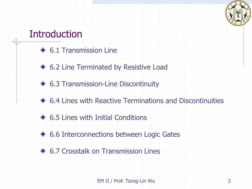
Introduction
6.1 Transmission Line 6.2 Line Terminated by Resistive Load
6.3 Transmission-Line Discontinuity 6.4 Lines with Reactive Terminations and Discontinuities 6.5 Lines with Initial Conditions
6.6 Interconnections between Logic Gates
6.7 Crosstalk on Transmission Lines
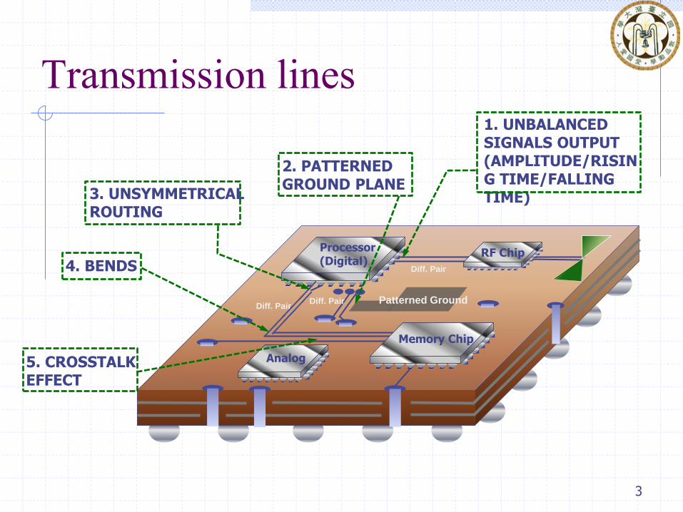
Transmission lines
3
Patterned Ground
RF Chip
Memory Chip
Processor (Digital)
Diff. Pair
Analog 5. CROSSTALK EFFECT
4. BENDS
3. UNSYMMETRICAL ROUTING
2. PATTERNED GROUND PLANE
1. UNBALANCED SIGNALS OUTPUT (AMPLITUDE/RISING TIME/FALLING TIME)
Diff. Pair
Diff. Pair

Trend of Differential Signaling
0
2
4
6
8
10
12
14
16
2008 2010 2012 2014 2016 2018 2020
Data
Rate
(G
b/s
)
Year
GDDR 5
USB 3.0
HDMI 1.3
SATA III
SATA IV
DDR 4
Display Port
2.0
1.8
1.6
1.4
1.2
1.0
0.8
0.6
0.4
Giga Ethernet PCI-E IV
DC
Lev
el (V)
Data: ITRS and IBM

Two Criterions for
Transmission Lines
Two conductors in homogeneous medium.
The conductors are electrically long.
5
Good engineering approximation: tr < 6td

Transmission-Line
Geometry
Shorted at the far end Discrete edge port of 50 Ω
Cross sectional view
time delay (td = 0.85 ns)
6

Cross sectional view
Transmission-Line
Surface Current
The wave is localized in a length
along the line and moves out in
space and time without changing
shape
time delay (td = 0.85 ns)
Shorted at the far end
7

Pulse Width (tp) = 4.25 ns
@ 5p dt t
Electrically Short Twin Lead
8
time delay (td = 0.85 ns )
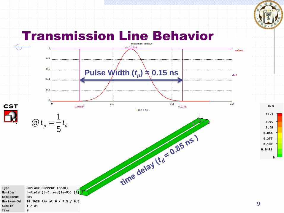
1@
5p dt t
Pulse Width (tp) = 0.15 ns
Transmission Line Behavior
9

Pulse Propagation
time delay (td = 0.85 ns )
Pulse Width (tp) = 0.85 ns
@ p dt t
10
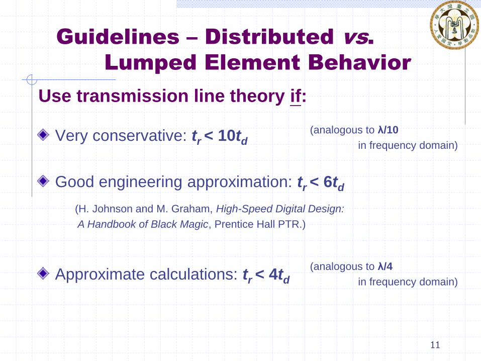
Guidelines – Distributed vs.
Lumped Element Behavior
Very conservative: tr < 10td
Good engineering approximation: tr < 6td
Approximate calculations: tr < 4td
Use transmission line theory if:
(H. Johnson and M. Graham, High-Speed Digital Design:
A Handbook of Black Magic, Prentice Hall PTR.)
(analogous to λ/10
in frequency domain)
(analogous to λ/4
in frequency domain)
11
EM II / Prof. Tzong-Lin Wu 12
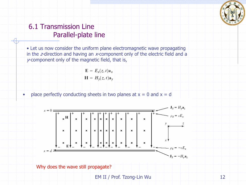
6.1 Transmission Line Parallel-plate line
• Let us now consider the uniform plane electromagnetic wave propagating in the z-direction and having an x-component only of the electric field and a y-component only of the magnetic field, that is,
• place perfectly conducting sheets in two planes at x = 0 and x = d
Why does the wave still propagate?

EM II / Prof. Tzong-Lin Wu 13
6.1 Transmission Line Parallel-plate line
Since the electric field is completely normal and the magnetic field is completely tangential to the sheets, the two boundary conditions the perfect conductors are satisfied, and, hence, the wave will simply propagate. What are the remaining two boundary conditions?
The wave propagation along the transmission line is supported by charges and currents on the plates, varying with time and distance along the line.
0 0[ ] [ ]x n x x x x xs E E a D a a
[ ] [ ]x d n x d x x x xs E E a D a a
0 0[ ] [ ]x n x x y y y zs H H J a H a a a
[ ] [ ]x d n x d x y y y zs H H J a H a a a

EM II / Prof. Tzong-Lin Wu 14
6.1 Transmission Line finite size parallel-plate line
Neglect fringing of the fields at the edges or assume that the structure is part of a much larger-sized configuration.
What important parameters can we define?
Voltage Current
What about the power?
0 0( , ) ( , ) ( , ) ( , )
d d
x x xx x
V z t E z t dx E z t dx dE z t
0 0 0( , ) ( , ) ( , ) ( , )
( , )
w w w
y yy y y
y
I z t Js z t dy H z t dy H z t dy
wH z t
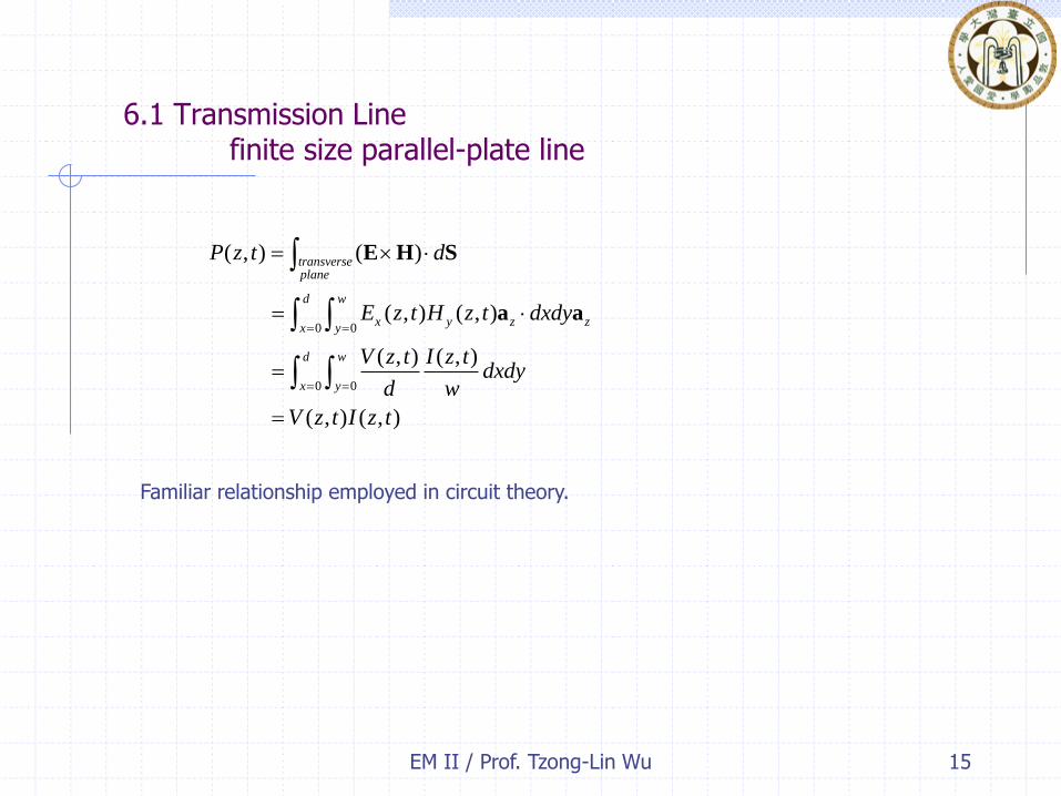
EM II / Prof. Tzong-Lin Wu 15
6.1 Transmission Line finite size parallel-plate line
Familiar relationship employed in circuit theory.
0 0
0 0
( , ) ( )
( , ) ( , )
( , ) ( , )
( , ) ( , )
transverseplane
d w
x y z zx y
d w
x y
P z t d
E z t H z t dxdy
V z t I z tdxdy
d w
V z t I z t
E H S
a a

EM II / Prof. Tzong-Lin Wu 16
6.1 Transmission Line transmission-line equations
Ex and Ey satisfy the two differential equations (see sec4.4)
They characterize the wave propagation along the line in terms of line voltage and line current instead of in terms of the fields.
y yxB HE
z t t
y x x
x
H E EE
z t t
x
VE
d
y
IH
w

EM II / Prof. Tzong-Lin Wu 17
6.1 Transmission Line transmission-line equations
Definitions of inductance and capacitance ?
L: The ratio of the magnetic flux per unit length at any value of z to the line current at that value of z.
C: The ratio of the magnitude of the charge per unit length on either plate at any value of z to the line voltage at that value of z.
Are L and C purely dependent on the dimensions of the line? Are they dependent on the Ex and Hy fields? Are L and C mutually independent ?
y
y
H d d
H w w
L
x
x
E w w
E d d
C

EM II / Prof. Tzong-Lin Wu 18
6.1 Transmission Line transmission-line equations
Replacing now the quantities in parentheses in (6.8a) and (6.8b) by L and C, respectively
These equations permit us to discuss wave propagation along the line in terms of circuit quantities instead of in terms of field quantities.
It should, however, not be forgotten that the actual phenomenon is one of electromagnetic waves guided by the conductors of the line.
L C
V I
z t
L
I V
z t
C

EM II / Prof. Tzong-Lin Wu 19
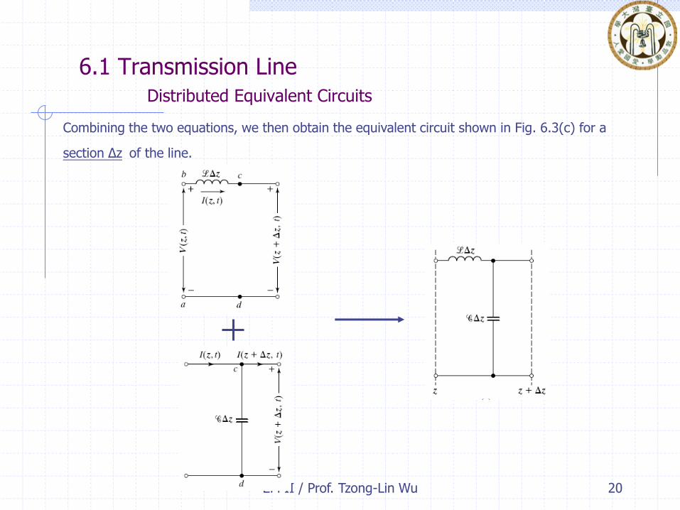
6.1 Transmission Line Distributed Equivalent Circuits
Transmission line equations -> transmission line equivalent circuits
This equation can be represented by the circuit equivalent shown in Fig. 6.3(a), since it satisfies Kirchhoff’s voltage law
written around the loop abcda.
This equation can be represented by the circuit equivalent shown in Fig. 6.3(b), since it satisfies Kirchhoff’s current law written for node c.
0
( , ) ( , ) ( , )limz
V z z t V z t I z t
z
L
t
( , )( , ) ( , )
I z tV z z t V z t z
t
L
0 0
( , ) ( , ) ( , )lim limz z
I z z t I z t V z z t
z
Ct
( , )( , ) ( , )
V z z tI z z t I z t z
t
C
EM II / Prof. Tzong-Lin Wu 20
6.1 Transmission Line Distributed Equivalent Circuits
Combining the two equations, we then obtain the equivalent circuit shown in Fig. 6.3(c) for a
section Δz of the line.
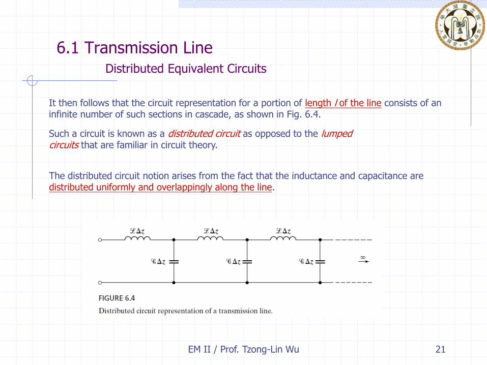
EM II / Prof. Tzong-Lin Wu 21
6.1 Transmission Line Distributed Equivalent Circuits
It then follows that the circuit representation for a portion of length l of the line consists of an infinite number of such sections in cascade, as shown in Fig. 6.4.
Such a circuit is known as a distributed circuit as opposed to the lumped circuits that are familiar in circuit theory.
The distributed circuit notion arises from the fact that the inductance and capacitance are distributed uniformly and overlappingly along the line.

EM II / Prof. Tzong-Lin Wu 22
6.1 Transmission Line Distributed Equivalent Circuits
Energy consideration -> distributed-circuit concept
If we consider a section of the line, the energy stored in the electric field in this section is given by
The energy stored in the magnetic field in that section is given by
We note that L and C are elements associated with energy storage in the magnetic field and energy storage in the electric field, respectively, for a given infinitesimal section of the line.
Since these phenomena occur continuously and since they overlap, the inductance and capacitance must be distributed uniformly and overlappingly along the line.
2 2
2 2
1 1(volume) ( )
2 2
1 1 ( )
2 2
e x x
x
W E E dw z
wE d z zV
d
C
2 2
2 2
1 1(volume) ( )
2 2
1 1 ( )
2 2
m y y
y
W H H dw z
dH w z zI
w
L
EM II / Prof. Tzong-Lin Wu 23
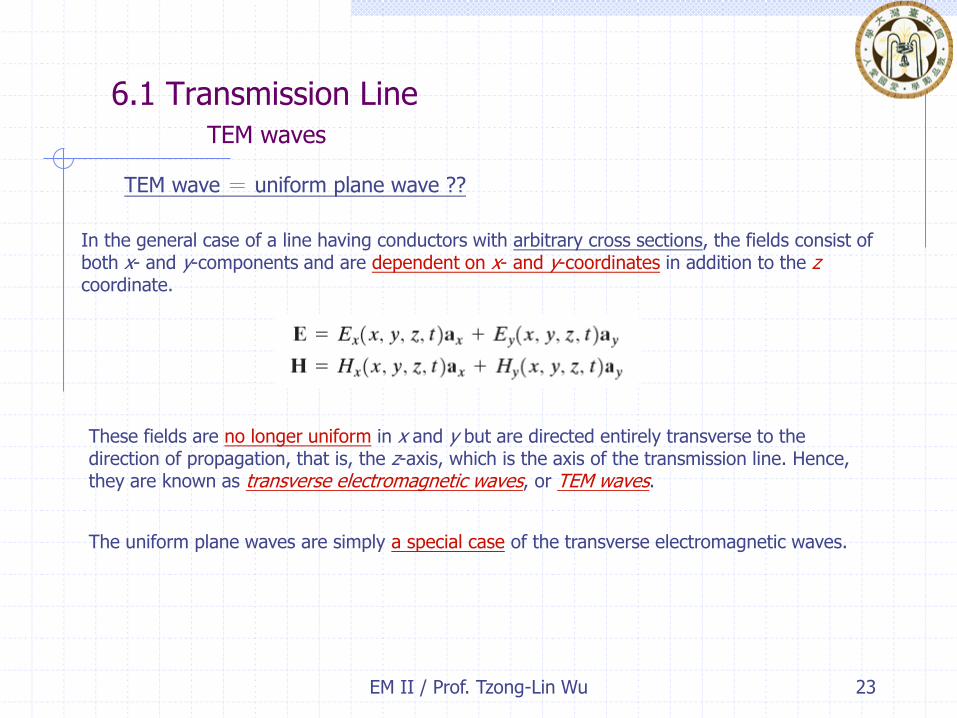
6.1 Transmission Line TEM waves
TEM wave = uniform plane wave ??
In the general case of a line having conductors with arbitrary cross sections, the fields consist of both x- and y-components and are dependent on x- and y-coordinates in addition to the z coordinate.
These fields are no longer uniform in x and y but are directed entirely transverse to the direction of propagation, that is, the z-axis, which is the axis of the transmission line. Hence, they are known as transverse electromagnetic waves, or TEM waves.
The uniform plane waves are simply a special case of the transverse electromagnetic waves.

EM II / Prof. Tzong-Lin Wu 24
6.1 Transmission Line TEM waves
Note: The transmission-line equations (6.12a) and (6.12b) and the distributed equivalent circuit of Fig. 6.4 hold for all transmission lines made of perfect conductors and perfect dielectric, that is, for all lossless transmission lines. What are their differences for different kind of transmission lines? The only differences are the line parameters L and C, which are dependent on the geometry of the lines. The values of L and C are the same as those obtainable from static field considerations. Why?
Since there is no z-component of H, the electric-field distribution in any given transverse plane at any given instant of time is the same as the static electric-field distribution resulting from the application of a potential difference between the conductors equal to the line voltage in that plane at that instant of time.
Similarly, since there is no z-component of E, the magnetic-field distribution in any given transverse plane at any given instant of time is the same as the static magnetic-field distribution resulting from current flow on the conductors equal to the line current in that plane at that instant of time.
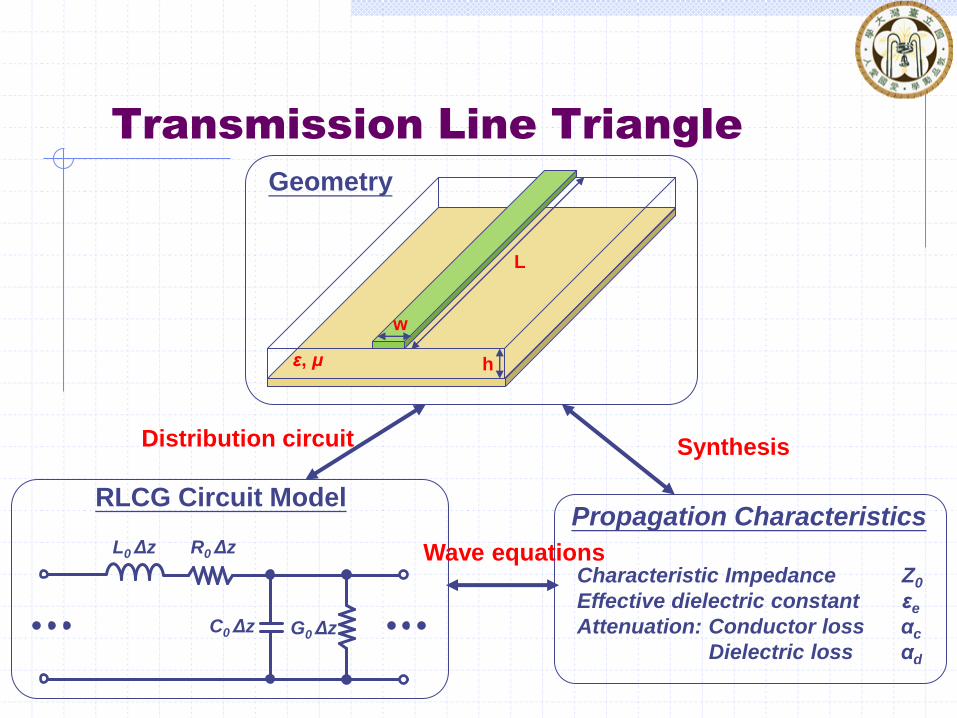
Transmission Line Triangle
Distribution circuit
h
w
L
ε, μ
Geometry
RLCG Circuit Model
L0 Δz R0 Δz
C0 Δz G0 Δz
Propagation Characteristics
Characteristic Impedance Z0
Effective dielectric constant εe
Attenuation: Conductor loss αc
Dielectric loss αd
Wave equations
Synthesis
EM II / Prof. Tzong-Lin Wu 26
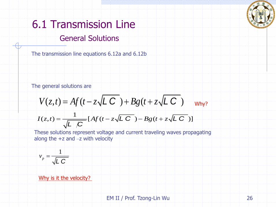
6.1 Transmission Line General Solutions
The transmission line equations 6.12a and 6.12b The general solutions are
These solutions represent voltage and current traveling waves propagating along the +z and –z with velocity
Why is it the velocity?
Why? ( , ) ( ) ( )V z t Af t z Bg t z L C L C
1( , ) [ ( ) ( )]I z t Af t z Bg t z L C L C
L C
1pv
L C

EM II / Prof. Tzong-Lin Wu 27
6.1 Transmission Line General Solutions
We, however, know that the velocity of propagation in terms of the dielectric parameters is given by
Therefore, it follows that
1pv
L C

EM II / Prof. Tzong-Lin Wu 28
6.1 Transmission Line Characteristic impedance
We now define the characteristic impedance of the line to be
so that (6.15a) and (6.15b) become
What is the physical meaning of the characteristic impedance?
The characteristic impedance is the ratio of the voltage to current in the (+) wave or the negative of the same ratio for the (-) wave. Note: It is analogous to the intrinsic impedance of the dielectric medium but not necessarily equal to it.
0Z L
C
( , ) ( ) ( )p p
z zV z t Af t Bg t
v v
0
1( , ) [ ( ) ( )]
p p
z zI z t Af t Bg t
Z v v
EM II / Prof. Tzong-Lin Wu 29
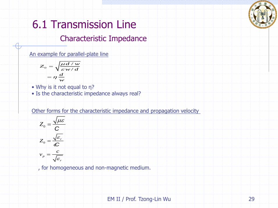
6.1 Transmission Line Characteristic Impedance
An example for parallel-plate line
• Why is it not equal to η? • Is the characteristic impedance always real?
Other forms for the characteristic impedance and propagation velocity
, for homogeneous and non-magnetic medium.
0
/
/
d wZ
w d
d
w
0Z
C
0
rZ
c
C
p
r
cv

EM II / Prof. Tzong-Lin Wu 30
6.1 Transmission Line Microstrip Line
If the cross section of a transmission line involves more than one dielectric, the situation corresponds to inhomogeneity. An example of this type of line is the microstrip line.
Note: it does not support the TEM wave because it is not possible to satisfy the boundary condition of equal phase velocities parallel to the air-dielectric interface with pure TEM waves How can we solve the propagation characteristics of the inhomogeneous transmission line? We assume the inhomogeneity has no effect on the per-unit-length inductance L and the propagation is TEM. Then, we solve two parameters:

EM II / Prof. Tzong-Lin Wu 31
6.1 Transmission Line Microstrip Line
C0 is the capacitance per unit length of the line with all the dielectrics replaced by free space from static field consideration. C is the capacitance per unit length of the line with the dielectrics in place and computed from static field considerations.
We define the effective relative permittivity as
0
eff
C
C
How can we find the C0 and C?
0
0
0 0
1Z
c
L CL
C CC CC
0 0
0
1 1pv c
C C
C CL C L C
0
effZ
c
C
p
eff
cv

EM II / Prof. Tzong-Lin Wu 32
6.1 Transmission Line Microstrip Line
A. Analytical Techniques
The analytical techniques are based on the closed-form solution of Laplace’s equation, subject to the
boundary conditions, or the equivalent of such a solution. We have already discussed these techniques in Sections 5.3 and 5.4 for several configurations.
B. Numerical Techniques
When a closed-form solution is not possible or when the approximation permitting a closed-form solution breaks down, numerical techniques can be employed. (chapter 11)
EM II / Prof. Tzong-Lin Wu 33
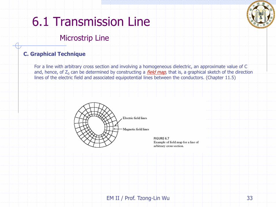
6.1 Transmission Line Microstrip Line
For a line with arbitrary cross section and involving a homogeneous dielectric, an approximate value of C and, hence, of Z0 can be determined by constructing a field map, that is, a graphical sketch of the direction lines of the electric field and associated equipotential lines between the conductors. (Chapter 11.5)
C. Graphical Technique

EM II / Prof. Tzong-Lin Wu 34
6.2 Line terminated by Resistive Loads Notation
General solutions to the transmission-line equations for the lossless line
What is the meaning of the negative sign of the current?
( , ) ( ) ( )p p
z zV z t V t V t
v v
0
1( , ) [ ( ) ( )]
p p
z zI z t V t V t
Z v v
V V V
0
1( )I V V
Z
I I I
0
VI
Z
0
VI
Z

EM II / Prof. Tzong-Lin Wu 35
6.2 Line terminated by Resistive Loads Notation
positive
The minus sign in (6.32b) indicates that is negative, and, hence, the wave power actually flows in the negative z-direction, as it should.
2
0 0
( )( )V V
P V I VZ Z
2
0 0
( )( )
V VP V I V
Z Z

EM II / Prof. Tzong-Lin Wu 36
6.2 Line terminated by Resistive Loads Excitation by a constant source
Let us now consider a line of length l terminated by a load resistance Rl and driven by a constant voltage source in series with internal resistance Rg
We assume that no voltage and current exist on the line for t < 0 and the switch S is closed at t = 0. A step transient wave is thus launched to the transmission line system.
What the impedance does the transient wave see at t = 0? What is the voltage amplitude on the transmission line at t = 0?
When the switch S is closed at a (+) wave originates at z = 0 and travels toward the load. Let the voltage and current of this (+) wave be V+ and I-, respectively.
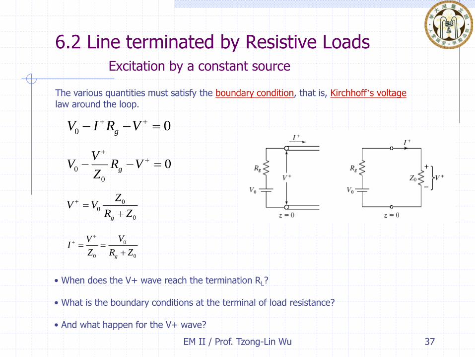
EM II / Prof. Tzong-Lin Wu 37
6.2 Line terminated by Resistive Loads Excitation by a constant source
The various quantities must satisfy the boundary condition, that is, Kirchhoff’s voltage
law around the loop.
• When does the V+ wave reach the termination RL?
• What is the boundary conditions at the terminal of load resistance?
• And what happen for the V+ wave?
0 0gV I R V
0
0
0g
VV R V
Z
0
0
0g
ZV V
R Z
0
0 0g
VVI
Z R Z

EM II / Prof. Tzong-Lin Wu 38
6.2 Line terminated by Resistive Loads Reflection coefficient
The wave travels toward the load and reaches the termination at t = l / Vp
The voltage across the load resistance to be equal to the current through it times its value RL, but the voltage-to-current ratio in the (+) wave is equal to Z0.
To resolve this inconsistency, there is only one possibility, which is the setting up of a (-) wave, or a reflected wave V-.
To satisfy the boundary condition,
Voltage reflection coefficient
Current reflection coefficient
( )LV V R I I
0 0
( )L
V VV V R
Z Z
0
0
L
L
R ZV V
R Z
0
0
L
L
R ZV
R ZV
0
0
V ZI V
I V Z V

EM II / Prof. Tzong-Lin Wu 39
6.2 Line terminated by Resistive Loads Reflection coefficient
We observe that this wave V- travels back toward the source and it reaches there at t = 2l / Vp.
Since the boundary condition at z = 0 which was satisfied by the original wave V+ alone, is then violated, a reflection of the reflection, or a re-reflection, will be set up and it travels toward the load.
To satisfy the boundary condition,
We note that the reflected wave views the source with internal resistance as the internal resistance alone; that is, the voltage source is equivalent to a short circuit insofar as the (-) wave is concerned.
0 ( )gV V V V R I I I
0
0
( )gR
V V V V V V VZ
0
0
g
g
R ZV V
R Z
EM II / Prof. Tzong-Lin Wu 40
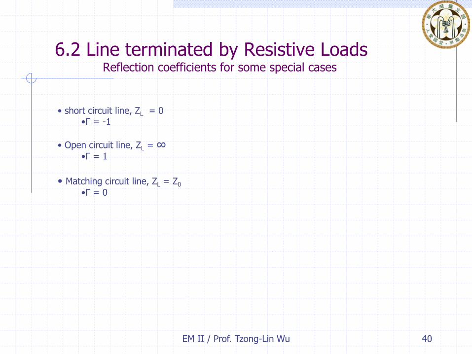
6.2 Line terminated by Resistive Loads Reflection coefficients for some special cases
• short circuit line, ZL = 0 •Γ = -1
• Open circuit line, ZL = ∞ •Γ = 1
• Matching circuit line, ZL = Z0
•Γ = 0
EM II / Prof. Tzong-Lin Wu 41
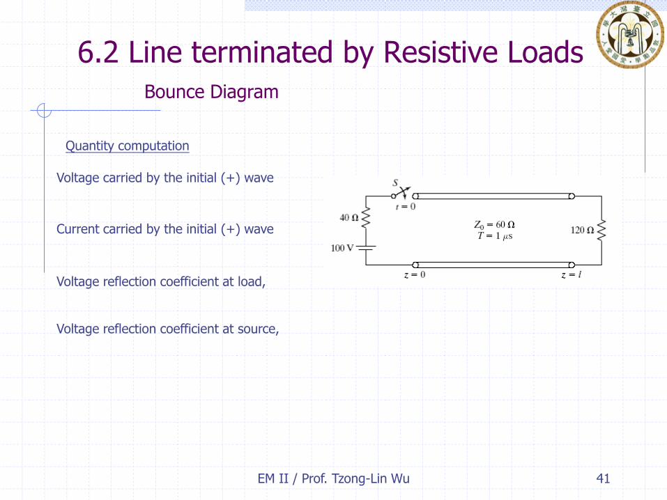
6.2 Line terminated by Resistive Loads Bounce Diagram
Quantity computation
Voltage carried by the initial (+) wave
Current carried by the initial (+) wave
Voltage reflection coefficient at load,
Voltage reflection coefficient at source,
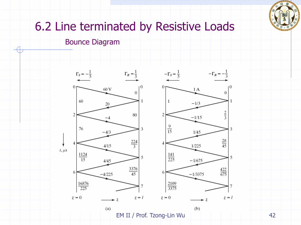
EM II / Prof. Tzong-Lin Wu 42
6.2 Line terminated by Resistive Loads Bounce Diagram

EM II / Prof. Tzong-Lin Wu 43
6.2 Line terminated by Resistive Loads Bounce Diagram
Plots of line voltage versus t (transient)
EM II / Prof. Tzong-Lin Wu 44
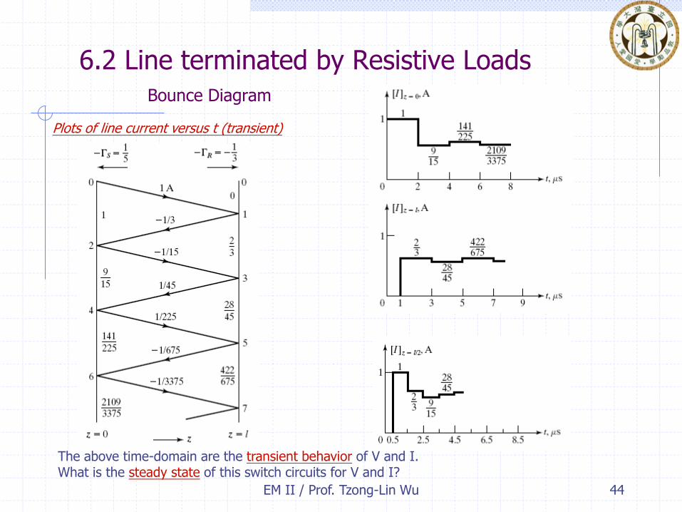
6.2 Line terminated by Resistive Loads Bounce Diagram
Plots of line current versus t (transient)
The above time-domain are the transient behavior of V and I. What is the steady state of this switch circuits for V and I?

EM II / Prof. Tzong-Lin Wu 45
6.2 Line terminated by Resistive Loads Bounce Diagram
Steady state
As time progresses, the line voltage and current tend to converge to certain values, which we can expect to be the steady state values.
In the steady state, the situation consists of a single (+) wave, which is actually a superposition of the infinite number of transient (+) waves, and a single (-) wave, which is actually a superposition of the infinite number of transient (-) waves.
The steady-state line voltage and current can now be obtained to be
Is there any intuitive concept to explain the results?

EM II / Prof. Tzong-Lin Wu 46
6.2 Line terminated by Resistive Loads Bounce Diagram
Plots of line voltage and current versus z
t = 2.5
+
+
+
EM II / Prof. Tzong-Lin Wu 47
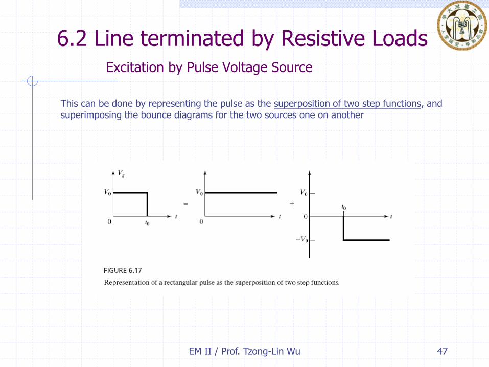
6.2 Line terminated by Resistive Loads Excitation by Pulse Voltage Source
This can be done by representing the pulse as the superposition of two step functions, and superimposing the bounce diagrams for the two sources one on another
EM II / Prof. Tzong-Lin Wu 48
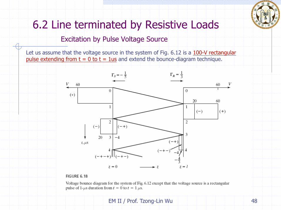
6.2 Line terminated by Resistive Loads Excitation by Pulse Voltage Source
Let us assume that the voltage source in the system of Fig. 6.12 is a 100-V rectangular pulse extending from t = 0 to t = 1us and extend the bounce-diagram technique.
EM II / Prof. Tzong-Lin Wu 49
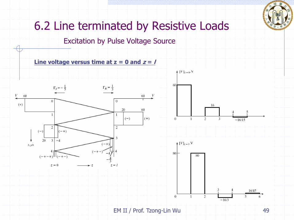
6.2 Line terminated by Resistive Loads Excitation by Pulse Voltage Source
Line voltage versus time at z = 0 and z = l

EM II / Prof. Tzong-Lin Wu 50
6.2 Line terminated by Resistive Loads Excitation by Pulse Voltage Source
Line voltage versus time at z = l/2
To draw the sketch for z = l/2, we displace the time plots of the (+) waves at z=0 and of the (-) waves at z =l forward in time by 0.5us that is, delay them by 0.5us and add them to obtain the plot.
Z=l/2

EM II / Prof. Tzong-Lin Wu 51
6.2 Line terminated by Resistive Loads Excitation by Pulse Voltage Source
t=2.25us
t=1.25us
Since the one-way travel time on the line is 1us,
we take the portion from t=2.25 back to t=1.25us.
Sketches of line voltage versus distance (z) along the line for fixed values of time
EM II / Prof. Tzong-Lin Wu 52
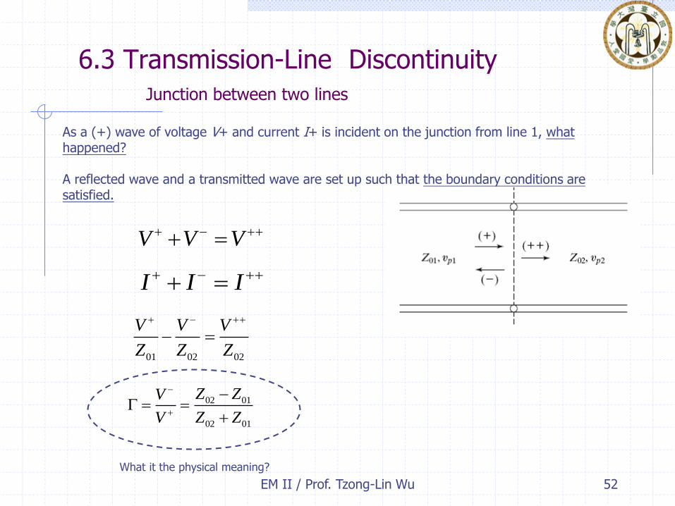
6.3 Transmission-Line Discontinuity Junction between two lines
As a (+) wave of voltage V+ and current I+ is incident on the junction from line 1, what happened? A reflected wave and a transmitted wave are set up such that the boundary conditions are satisfied.
V V V
I I I
01 02 02
V V V
Z Z Z
02 01
02 01
Z ZV
Z ZV
What it the physical meaning?

EM II / Prof. Tzong-Lin Wu 53
6.3 Transmission-Line Discontinuity Junction between two lines
Thus, to the incident wave, the transmission line to the right in (a) looks like its characteristic impedance as shown in (b).
(a) (b) Note: What is the difference between (a) and (b)? A resistive load (50 ohm for example) and the transmission line load (Z0 = 50 ohm)
power is dissipated in the load v.s. the power is transmitted into the line
EM II / Prof. Tzong-Lin Wu 54
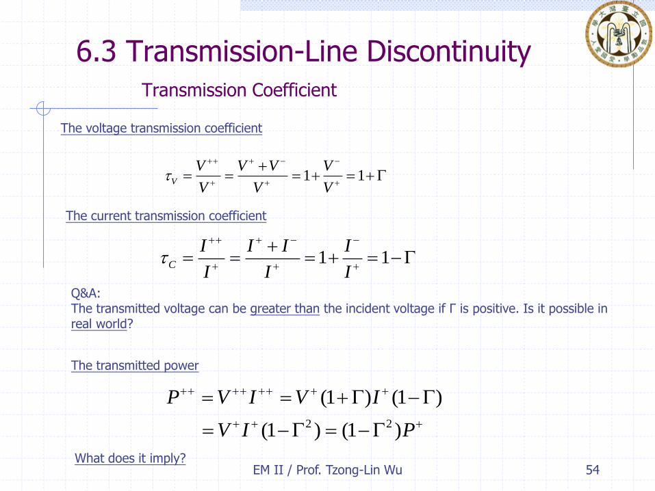
6.3 Transmission-Line Discontinuity Transmission Coefficient
The voltage transmission coefficient
1 1V
V V V V
V V V
1 1C
I I I I
I I I
2 2
(1 ) (1 )
(1 ) (1 )
P V I V I
V I P
The current transmission coefficient
Q&A: The transmitted voltage can be greater than the incident voltage if Γ is positive. Is it possible in real world?
The transmitted power
What does it imply?
EM II / Prof. Tzong-Lin Wu 55
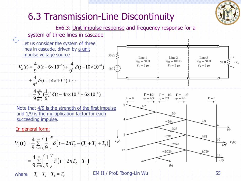
6.3 Transmission-Line Discontinuity Ex6.3: Unit impulse response and frequency response for a
system of three lines in cascade
6 6
2
6
3
6 6
0
4 4( ) ( 6 10 ) ( 10 10 )
9 9
4 + ( 14 10 )
9
4 1 ( ) ( 4 10 6 10 )
9 9
o
n
n
V t t t
t
t n
Note that 4/9 is the strength of the first impulse and 1/9 is the multiplication factor for each succeeding impulse.
Let us consider the system of three lines in cascade, driven by a unit impulse voltage source
0 2 1 2 30
2 00
4 1( ) 2 ( )
9 9
4 12
9 9
n
n
n
n
V t t nT T T T
t nT T
In general form:
where 1 2 3 0T T T T

EM II / Prof. Tzong-Lin Wu 56
6.3 Transmission-Line Discontinuity Junction between two lines
2/m T
Frequency response
0 2 00
4 1( ) cos 2
9 9
n
n
V t t nT T
2 0
0 2
0
2
(2 )
00
0
2
4 1( )
9 9
4 1
9 9
(4 / 9)
1 (1/ 9)
n
j nT T
n
n
j T j T
n
j T
j T
V e
e e
e
e
Assume input is sinusoidal
2(2 1) / 2m T
Maximum occurs at
Minimum occurs at
2/m T
4 1/(1 ) 0.5
9 9
4 1/(1 ) 0.4
9 9
its value
its value

EM II / Prof. Tzong-Lin Wu 57
6.3 Transmission-Line Discontinuity Junction between two lines
Radome : an enclosure for protecting an antenna from the weather while allowing transparency for electromagnetic waves.
A simple, idealized, planar version of the radome is a dielectric slab with free space on either side of it.
The arrangement is equivalent to three lines in cascade, with the characteristic impedances equal to the intrinsic impedances of the media and the velocities of propagation equal to those in the media.
The amplitude versus frequency response is of the same form as previous example, where T2 is the one-way travel time in the dielectric slab and the maximum is 1 instead of 0.5. (the factor of 0.5 in previous example is due to voltage drop across the internal resistance of the source in the transmission-line system)
2/ / r rT c l
The lowest frequency for which the dielectric slab is completely transparent is

EM II / Prof. Tzong-Lin Wu 58
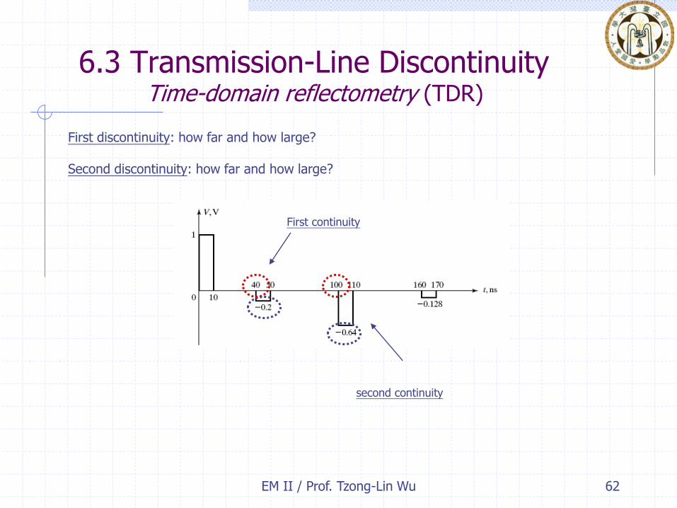
6.3 Transmission-Line Discontinuity Time-domain reflectometry (TDR)
What is the purpose of the matched attenuator?
The matched attenuator serves the purpose of absorbing the pulses arriving back from the system so that reflections of those pulses are not produced
TDR, a technique by means of which discontinuities in transmission-line systems can be located by making measurements with pulses.

Time Domain Reflectometry
Bandwidth: 20GHz
Min. rising time: 38ps
Calibration of error in TDR
measurement is quite important
generator
Tee DUT
Digital oscilloscope
Ei Er
Et
trigger 59

EM II / Prof. Tzong-Lin Wu 60
6.3 Transmission-Line Discontinuity Time-domain reflectometry (TDR)
A discontinuity exists at z = 4m and the line is short-circuited at the far end.
Assuming the TDR pulses to be of amplitude 1 V, duration 10 ns, and repetition rate Hz. We shall then discuss how one can deduce the information about the discontinuity from the TDR measurement.
510

EM II / Prof. Tzong-Lin Wu 61
6.3 Transmission-Line Discontinuity Time-domain reflectometry (TDR)
Can you predict the discontinuity situations from the measured voltage waveform on the TDR?
EM II / Prof. Tzong-Lin Wu 62
6.3 Transmission-Line Discontinuity Time-domain reflectometry (TDR)
First discontinuity: how far and how large? Second discontinuity: how far and how large?
First continuity
second continuity

EM II / Prof. Tzong-Lin Wu 63
6.4 Line with reactive terminations and discontinuities Inductive termination
A line of length l is terminated by an inductor L with zero initial current and a constant-voltage source with internal resistance equal to the characteristic impedance of the line is connected to the line at t = 0.
0
0 2
VL dVV
Z dt
0
0 0
02
t T
V V
Z Z
0
2t T
VV
0( / )0
2
Z L tVV Ae
The boundary condition at z = l
0 0
0 02 2
V Vd VV L
dt Z Z
Initial condition
0( / )
0
Z L TA V e
Solution:
0( / )( )00( , )
2
Z L t TVV l t V e for t T

EM II / Prof. Tzong-Lin Wu 64
6.4 Line with reactive terminations and discontinuities Inductive termination
0
0
( / )( )
0
( , ) ( , )2
0Z L t T
VV l t V l t
for t T
V e for t T
0
0
0
( / )( )
0 0
( , ) ( , )2
0
( / ) 1Z L t T
VI l t I l t
Z
for t T
V Z e for t T
Can you predict the waveform behavior by an intuitive physical concept?

EM II / Prof. Tzong-Lin Wu 65
6.4 Line with reactive terminations and discontinuities Inductive termination
The inductor is looked as 1. Short circuit at steady state t = infinite. 2. Open circuit at initial transient for t = T. Between t = T and t = infinite, the behavior follows the time constant L/Z0.
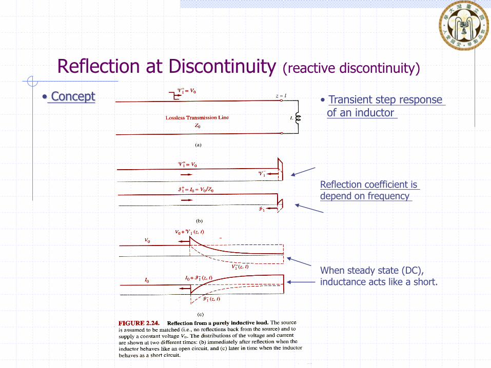
Reflection at Discontinuity (reactive discontinuity)
• Transient step response of an inductor
Reflection coefficient is depend on frequency
When steady state (DC), inductance acts like a short.
• Concept
EM II / Prof. Tzong-Lin Wu 67
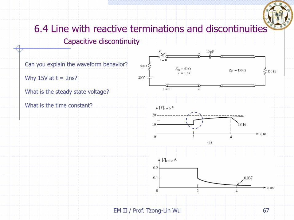
6.4 Line with reactive terminations and discontinuities Capacitive discontinuity
Can you explain the waveform behavior? Why 15V at t = 2ns? What is the steady state voltage? What is the time constant?

TDR signatures produced by simple discontinuities
EM II / Prof. Tzong-Lin Wu 69
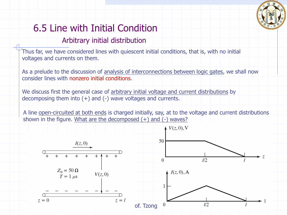
6.5 Line with Initial Condition Arbitrary initial distribution
Thus far, we have considered lines with quiescent initial conditions, that is, with no initial voltages and currents on them. As a prelude to the discussion of analysis of interconnections between logic gates, we shall now consider lines with nonzero initial conditions. We discuss first the general case of arbitrary initial voltage and current distributions by decomposing them into (+) and (-) wave voltages and currents.
A line open-circuited at both ends is charged initially, say, at to the voltage and current distributions shown in the figure. What are the decomposed (+) and (-) waves?
EM II / Prof. Tzong-Lin Wu 70
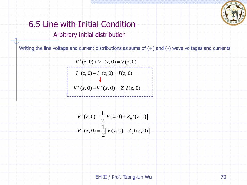
6.5 Line with Initial Condition Arbitrary initial distribution
( , 0) ( , 0) ( , 0)V z V z V z
( , 0) ( , 0) ( , 0)I z I z I z
0( , 0) ( , 0) ( , 0)V z V z Z I z
0
1( , 0) ( , 0) ( , 0)
2V z V z Z I z
0
1( , 0) ( , 0) ( , 0)
2V z V z Z I z
Writing the line voltage and current distributions as sums of (+) and (-) wave voltages and currents

EM II / Prof. Tzong-Lin Wu 71
6.5 Line with Initial Condition Arbitrary initial distribution
t = 0
Can you plot the (+) and (-) waveform at t = 0.5us?

EM II / Prof. Tzong-Lin Wu 72
6.5 Line with Initial Condition Arbitrary initial distribution
Key concept: voltage reflection coefficient of 1 and current reflection coefficient of -1 at both ends.
voltage

EM II / Prof. Tzong-Lin Wu 73
6.5 Line with Initial Condition Arbitrary initial distribution
current
EM II / Prof. Tzong-Lin Wu 74
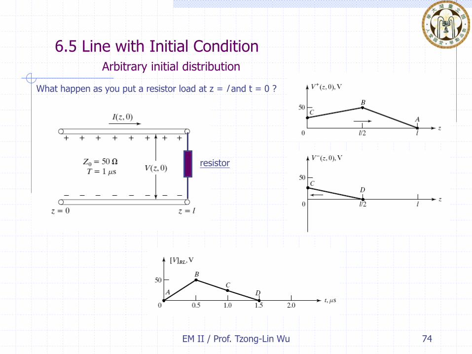
6.5 Line with Initial Condition Arbitrary initial distribution
What happen as you put a resistor load at z = l and t = 0 ?
resistor

EM II / Prof. Tzong-Lin Wu 75
6.5 Line with Initial Condition uniform initial distribution (ex: 6.6)
The analysis can be carried out with the aid of superposition and bounce diagrams.
What happened as the switch is on at t = 0 ? Can you plot the voltage v.s. time on the RL?
0 LV V R I
0
0
LRV V V
Z
00
0L
ZV V
R Z
0
0
1
L
I VR Z

EM II / Prof. Tzong-Lin Wu 76
6.5 Line with Initial Condition uniform initial distribution (ex: 6.6)
Bounce diagram
Is the energy balanced between t = 0- and t = 0+? What is the stored energy at t = 0- ? Where does the energy go at t > 0 ?

EM II / Prof. Tzong-Lin Wu 77
6.5 Line with Initial Condition uniform initial distribution (ex: 6.6)
At t = 0-, energy is stored in both electric and magnetic fields in the line, with energy densities ½ C V2 and ½ L I2 respectively.
2 2
0 0
22 0
0
0
4
1 1
2 2
1 1 1
2 2
10
e pW V l V v T
VV T T
Z
J
LC
C C
C
2 2
0 0
2 2
0 0 0
1 1
2 2
1 1 1
2 2
0
m pW I l I v T
I T I Z T
LC
L L
L
After t = 0,
0 0( 100 , 0, 1 )V V I T s
Power is conservative!
EM II / Prof. Tzong-Lin Wu 78
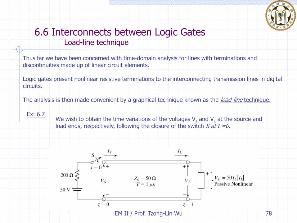
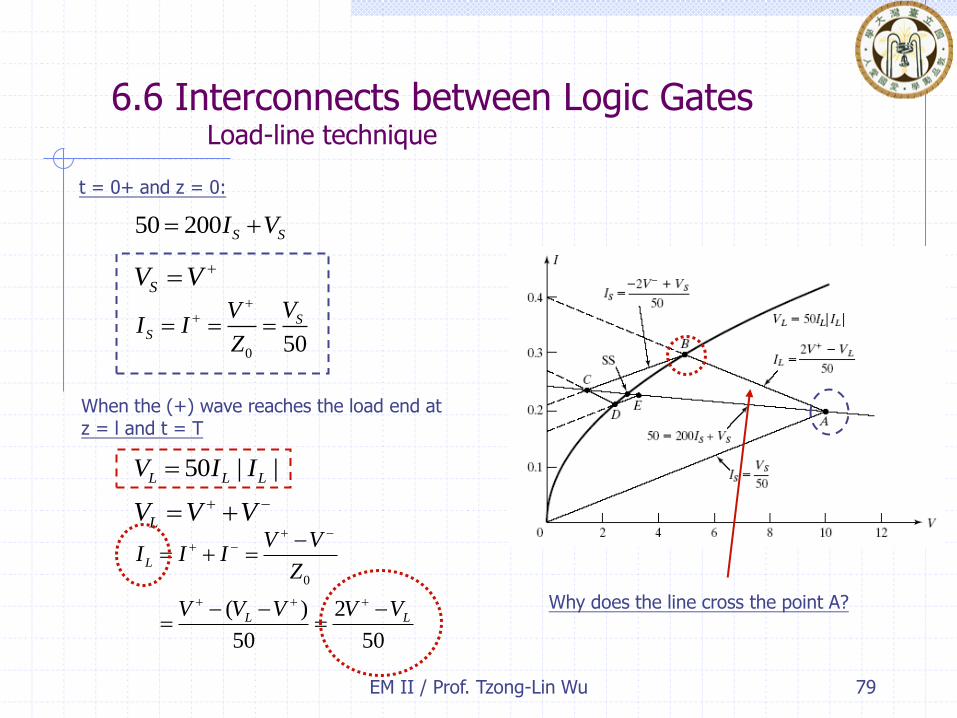
6.6 Interconnects between Logic Gates Load-line technique
Thus far we have been concerned with time-domain analysis for lines with terminations and discontinuities made up of linear circuit elements. Logic gates present nonlinear resistive terminations to the interconnecting transmission lines in digital circuits. The analysis is then made convenient by a graphical technique known as the load-line technique.
Ex: 6.7 We wish to obtain the time variations of the voltages Vs and VL at the source and load ends, respectively, following the closure of the switch S at t =0.
EM II / Prof. Tzong-Lin Wu 79
6.6 Interconnects between Logic Gates Load-line technique
50 200 S SI V
t = 0+ and z = 0:
SV V
0 50
SS
VVI I
Z
50 | |L L LV I I
LV V V
0
( ) 2
50 50
L
L L
V VI I I
Z
V V V V V
When the (+) wave reaches the load end at z = l and t = T
Why does the line cross the point A?
EM II / Prof. Tzong-Lin Wu 80
6.6 Interconnects between Logic Gates Load-line technique
LV V
/ 50LI I
Noting in the equation (2 ) /50L LI V V
Setting Then Thus, the point A is also on this line
When the (-) wave reaches the source end at z = 0 and t = 2T, it sets up a reflection.
SV V V V
0
2
50 50
S
S S
V V VI I I I
Z
V V V V V V V
50 200 S SI V
Why does the line cross the point B?

EM II / Prof. Tzong-Lin Wu 81
6.6 Interconnects between Logic Gates Load-line technique
( 2 ) /50s sI V V Note that
sV V V ( ) / 50sI V V
For We can obtain Thus, this line crosses point B.
Continuing in this manner, we observe that the solution consists of obtaining the points of intersection on the source and load V-I characteristics by drawing successively straight lines of slope 1/Z0 and -1/Z0 and beginning at the origin (the initial state) and with each straight line originating at the previous point of intersection.

EM II / Prof. Tzong-Lin Wu 82
6.6 Interconnects between Logic Gates Load-line technique
Output waveform at source and load

EM II / Prof. Tzong-Lin Wu 83
6.6 Interconnects between Logic Gates Load-line technique – uniformed charged line
Why start here?
The voltage at which side?
EM II / Prof. Tzong-Lin Wu 84
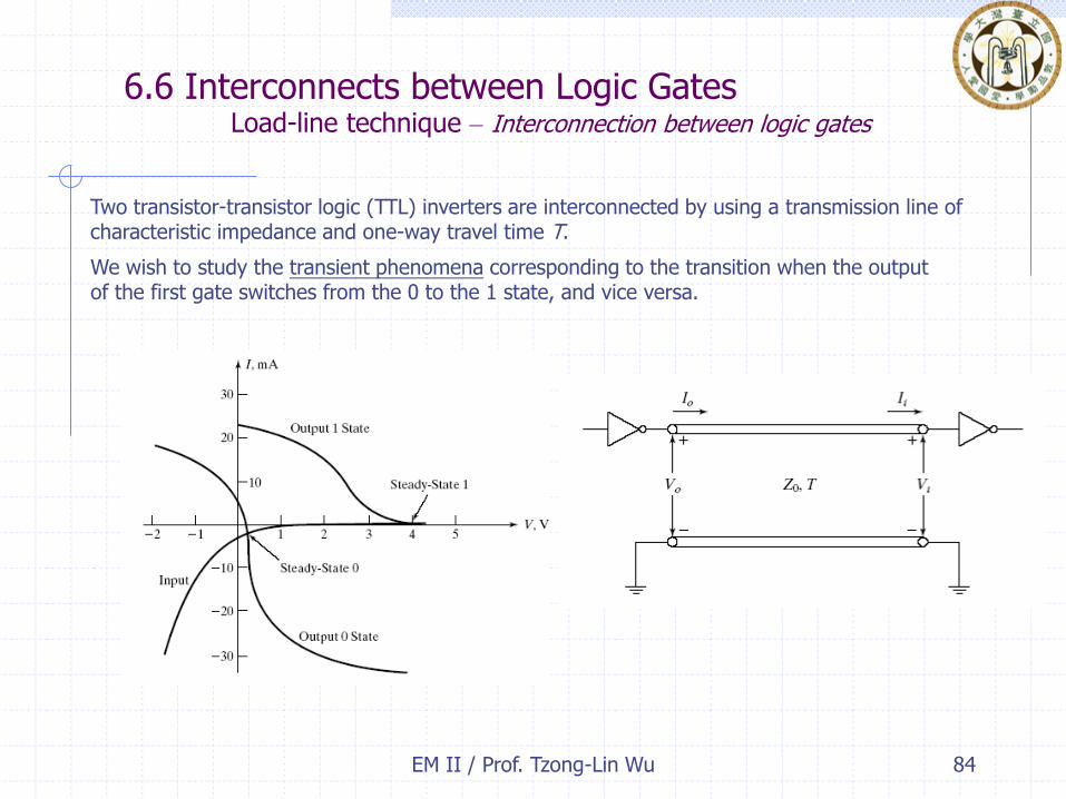
6.6 Interconnects between Logic Gates Load-line technique – Interconnection between logic gates
Two transistor-transistor logic (TTL) inverters are interconnected by using a transmission line of characteristic impedance and one-way travel time T.
We wish to study the transient phenomena corresponding to the transition when the output of the first gate switches from the 0 to the 1 state, and vice versa.

EM II / Prof. Tzong-Lin Wu 85
6.6 Interconnects between Logic Gates Load-line technique – Interconnection between logic gates
Analysis of 0-to-1 transition
EM II / Prof. Tzong-Lin Wu 86
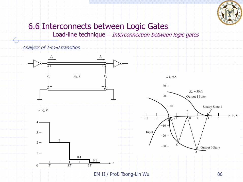
6.6 Interconnects between Logic Gates Load-line technique – Interconnection between logic gates
Analysis of 1-to-0 transition
EM II / Prof. Tzong-Lin Wu 87
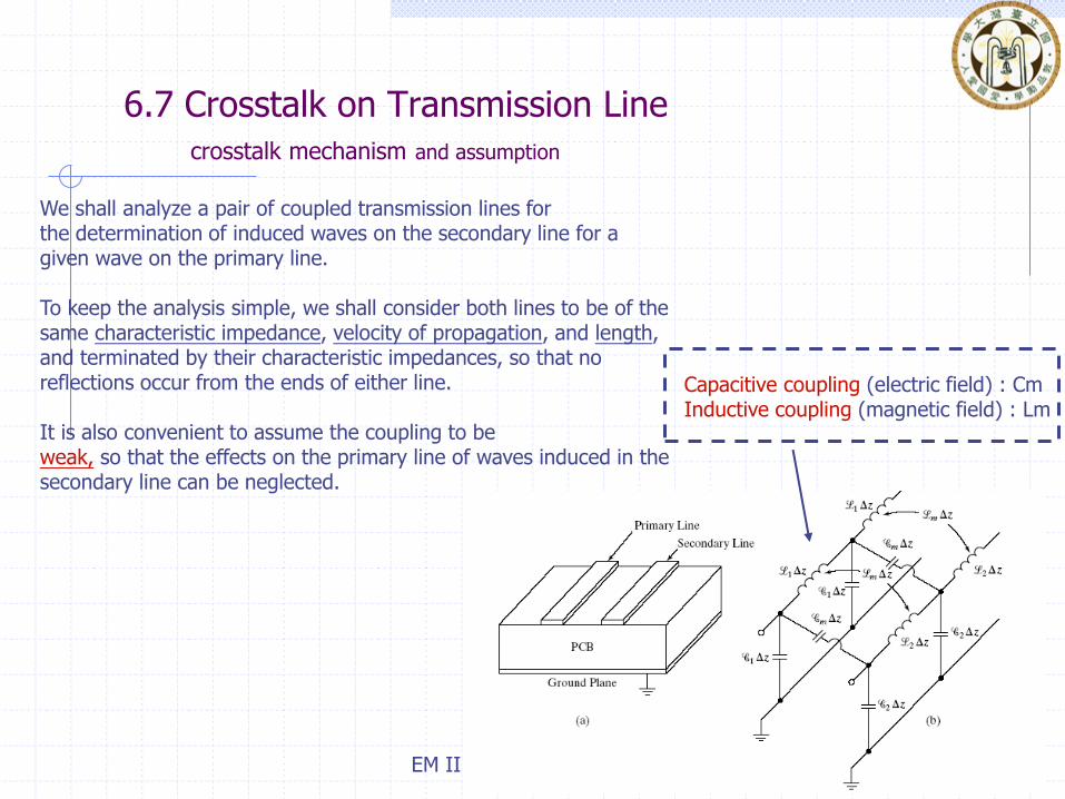
6.7 Crosstalk on Transmission Line crosstalk mechanism and assumption
We shall analyze a pair of coupled transmission lines for the determination of induced waves on the secondary line for a given wave on the primary line. To keep the analysis simple, we shall consider both lines to be of the same characteristic impedance, velocity of propagation, and length, and terminated by their characteristic impedances, so that no reflections occur from the ends of either line. It is also convenient to assume the coupling to be weak, so that the effects on the primary line of waves induced in the secondary line can be neglected.
Capacitive coupling (electric field) : Cm Inductive coupling (magnetic field) : Lm
EM II / Prof. Tzong-Lin Wu 88
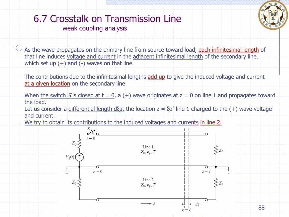
6.7 Crosstalk on Transmission Line weak coupling analysis
As the wave propagates on the primary line from source toward load, each infinitesimal length of that line induces voltage and current in the adjacent infinitesimal length of the secondary line, which set up (+) and (-) waves on that line. The contributions due to the infinitesimal lengths add up to give the induced voltage and current at a given location on the secondary line
When the switch S is closed at t = 0, a (+) wave originates at z = 0 on line 1 and propagates toward the load. Let us consider a differential length dξat the location z = ξof line 1 charged to the (+) wave voltage and current. We try to obtain its contributions to the induced voltages and currents in line 2.

EM II / Prof. Tzong-Lin Wu 89
6.7 Crosstalk on Transmission Line modeling for capacitive coupling
12
( , )( , )c m
V tI t
t
C
Equivalent circuit

EM II / Prof. Tzong-Lin Wu 90
6.7 Crosstalk on Transmission Line modeling for inductive coupling
12
( , )( , )c m
I tV t
t
L

EM II / Prof. Tzong-Lin Wu 91
6.7 Crosstalk on Transmission Line modeling for inductive coupling
2 0 2 2
1 1
2 2c cV Z I V
1 12 0
10
0
( , ) ( , )1 1( , )
2 2
( , )1
2
m m
mm
V t I tV t Z
t t
V tZ
Z t
C L
LC
12 0
0
( , )1( , )
2
mm
V tV t Z
Z t
LC
2 0 2 2
1 1
2 2c cV Z I V
Combining the contributions due to capacitive coupling and inductive coupling

EM II / Prof. Tzong-Lin Wu 92
6.7 Crosstalk on Transmission Line forward crosstalk voltage and current
Noting that the effect of V1 at z = ξ at a given time t is felt at a location z >ξ on line 2 at time t + (z – ξ) / vp. we can write
2 0 10
0
1
0 0
0
1( , )
2
/1
2
z mm
p p
pzmm
zV z t Z V t d
Z t v v
V t z vZ d
Z t
LC
LC
'
2 1( , ) ( / )f pV z t zK V t z v
0
0
1
2
mf mK Z
Z
LC
Note that the upper limit in the integral is z, because the line-1 voltage to the right of a given location z on that line does not contribute to the forward-crosstalk voltage on line 2 at that same location.
forward-crosstalk coefficient
EM II / Prof. Tzong-Lin Wu 93
6.7 Crosstalk on Transmission Line backward crosstalk voltage and current
Noting that the effect of V1 at z = ξ at a given time t is felt at a location z <ξ on line 2 at
time t + (ξ - z) / vp.
2 0 1
0
0 1
0
0 1
0
0 1
0
1( , )
2
1 2
2
1 2
4
1
4
l mmz
p p
lmm z
p p
lmp m z
p p
mp m
zV z t Z V t d
Z t v v
zZ V t d
Z t v v
zv Z V t d
Z v v
zv Z V t
Z
LC
LC
LC
LC
2l
p pz
v v
2 1 1
2( , ) b
p p p
z l zV z t K V t V t
v v v
0
0
1
4
mb p mK v Z
Z
LC
backward-crosstalk coefficient
The lower limit in the integral is z, because the line-1 voltage to the left of a given location z on that line does not contribute to the backward crosstalk voltage on line 2 at that same location.
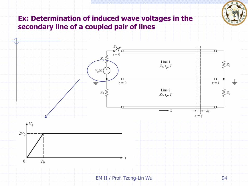
Ex: Determination of induced wave voltages in the secondary line of a coupled pair of lines
EM II / Prof. Tzong-Lin Wu 94

Ex: Determination of induced wave voltages in the secondary line of a coupled pair of lines
EM II / Prof. Tzong-Lin Wu 95
Far end

Ex: Determination of induced wave voltages in the secondary line of a coupled pair of lines
EM II / Prof. Tzong-Lin Wu 96
Near End

Ex: Determination of induced wave voltages in the secondary line of a coupled pair of lines
EM II / Prof. Tzong-Lin Wu 97