Electron Microscopy - Scanning electron microscope, Transmission Electron Microscope
Transmission Electron Microscopy(TEM)
Transmission Electron Microscopy (TEM) is a well known technique
for imaging solid materials at atomic resolution. Structural information
can be acquired both by (high resolution) imaging as well as by
electron diffraction. Additional detectors allow for elemental and
chemical analysis down to this sub-nanometer scale.
• atomic resolution
• morphology
• crystal structure
• element mapping
• composition profiling
• 3-D morphology
Philips Innovation labs

Basic principles
The design of a transmission electron
microscope (TEM) is analogous to that of an
optical microscope. In a TEM high-energy
(>100 kV) electrons are used instead of
photons and electromagnetic lenses instead
of glass lenses. The electron beam passes an
electron-transparent sample and a magnified
image is formed using a set of lenses. This
image is projected onto a fluorescent screen
or a CCD camera. Whereas the use of visible
light limits the lateral resolution in an optical
microscope to a few tenths of a micrometer,
the much smaller wavelength of electrons
allows for a resolution of 0.2 nm in a TEM.
Imaging
Image contrast is obtained by interaction of
the electron beam with the sample. Several
contrast effects play a role. In the resulting
TEM image denser areas and areas
containing heavier elements appear darker
due to scattering of the electrons in the
sample. In addition, scattering from crystal
planes introduces diffraction contrast. This
contrast depends on the orientation of a
crystalline area in the sample with respect
to the electron beam. As a result, in a TEM
image of a sample consisting of randomly
oriented crystals each crystal will have its
own grey-level. In this way one can
distinguish between different materials, as
well as image individual crystals and crystal
defects. Because of the high resolution of
the TEM, atomic arrangements in crystalline
structures can be imaged in large detail
(figure 1).
Electron diffraction
In case of a crystalline material, electron
diffraction will only occur at specific angles,
which are characteristic for the crystal
structure present. As a result, a diffraction
pattern of the irradiated area is created that
can be projected onto the CCD camera. In
this way, electron diffraction can provide
crystallographic information from thin films
(see figure 2), bulk materials as well as from
nanometer sized particles.
Chemical analysis
As a result of the interaction of the electron
beam with the specimen, some energy is
transferred from the electrons to the
sample. The excitation and de-excitation of
atoms and molecules in the sample allow
(local) chemical analysis.
This analysis can either be performed using
the broad beam used for normal imaging, or
by focusing the beam size down to 0.2 nm.
The combination of Scanning TEM (STEM), a
mode in which this narrow beam scans a
selected area of the specimen, with
chemical analysis techniques such as
Electron Energy Loss Spectroscopy (EELS)
and Energy Dispersive X-Ray analysis (EDX)
allows for mapping of the lateral distribution
of elements with high spatial resolution.
Electron Energy Loss Spectroscopy (EELS)
When travelling through the sample the
electrons may lose energy due to (multiple)
inelastic scattering events. The amount of
energy that is transferred from the incident
electron to the sample is dependent on the
composition of the sample. Because the
primary beam of electrons has one
well-defined energy, the spectrum of the
electrons that have passed the sample
contains chemical information on the
irradiated area. This principle is used in
both EELS and Energy Filtered TEM
(EFTEM).
Using EELS an energy loss spectrum is
acquired, such as shown in figure 3.
Quantification of the spectrum enables
determination of (local) concentrations of
elements. The fine structure in the EELS
spectra provides information on the
chemical binding of the atoms involved. The
combination of EELS and STEM allows for
1-D and 2-D mapping of the lateral
distribution of elements.
10 nm
Fig. 2: Electron diffraction patterns of an as-deposited
(room temperature) and an annealed (300 ºC) Al-Ge
film. The left part shows a set of a few, broad rings,
characteristic of an amorphous film. The right part
shows a large number of sharp rings. The diameters
of these rings are characteristic for the crystal
structure present. In this case a mixture of crystalline
Al and crystalline Ge.
Fig. 1: High resolution TEM image of a multi-walled
carbon nanowire.The wire consists of segments,
bounded by inner segment boundaries, see arrow.

Energy Filtered TEM (EFTEM)
A special filter on the TEM allows for
selection of a very narrow window of
energies in the EELS spectrum. Using the
corresponding electrons for imaging, EFTEM
is performed. The resulting image is formed
by electrons with one element-specific
energy loss. As a result, a qualitative
elemental map is obtained. (see figure 4).
EFTEM is the only chemical analysis
procedure in the TEM that does not use a
scanning beam. As a consequence, it is much
faster.
Fig. 5: HAADF image of a MOS transistor on SOI.
Due to Z-contrast the SiO2 , silicon and NiSi areas
appear dark grey, light grey, and white respectively.
Energy Dispersive X-ray analysis (EDX)
As a result of the interaction of the incident
electron beam with the sample, X-rays are
emitted. Their energies are characteristic
for the atoms present in the volume that is
probed. The detection and analysis of these
X-rays is called Energy Dispersive X-Ray
analysis. The X-ray spectrum that is
obtained allows for quantification of the
elemental composition of the irradiated
area. The combination of EDX and STEM
allows for mapping of the lateral distribution
of elements. A typical example is shown in
figures 6 and 7.
Fig. 6: A color map displaying the elemental
distributions of O (red), Ni (blue) and As (green)
within the red box in figure 5. In each of the
1250 pixels of 2×2 nm2 the compositions were
determined quantitatively by EDX.
HAADF
Another way of obtaining compositional as
well as structural information using TEM is
High Angle Annular Dark Field (HAADF)
imaging. For this application a dedicated
detector is used that only collects electrons
that are elastically scattered over large
angles by the specimen. The intensity that is
detected is dependent on the average
atomic number Z present in the irradiated
area: I ~ Z2. In combination with STEM,
mass contrast images can be acquired down
to atomic resolution. (see figure 5).
Fig. 7: Graph displaying the elemental concentrations
of As, O, N, and Si along the line in figure 6.
Fig. 3: EELS spectrum acquired from the segment-boundary shown in
figure 1. Quantification yielded 5-7 atomic % of N in this segment
boundary, whereas in the outer walls only 1-3 % of N is present.
inte
nsity
(a.
u.)
Energy loss (eV)
raw data
quantified data
C
N
200 700500400 600300
0,2 µm
Fig. 4: A color map, combining EFTEM images
acquired at the characteristic energy losses of Si,
Cu and Ta. Here, a cross-section of a copper line is
shown that is running perpendicular to the plane of
view. The result of electro-migration is visible: due
to electrical stress copper has migrated through the
Ta barrier layer into the neighboring areas.
50 nm
conc
entr
atio
n (a
tom
ic %
)
distance (nm)
0
10
0 503010
20
30
40
50
60
70
80
90
O
Ni
Si
As
©2016 Philips Lighting Holding B.V.All rights reserved.
Philips Innovation labs
Material Analysis lab
offers a full range of analytical methods and
expertise to support both research and
manufacturing, serving customers by taking
an integral, solution-oriented approach.
World-class expertise – working for youFor more information:
Phone: +31 40 27 40455
E-mail: [email protected]
www.innovationlabs.philips.com
Technical Note 7
August 2016
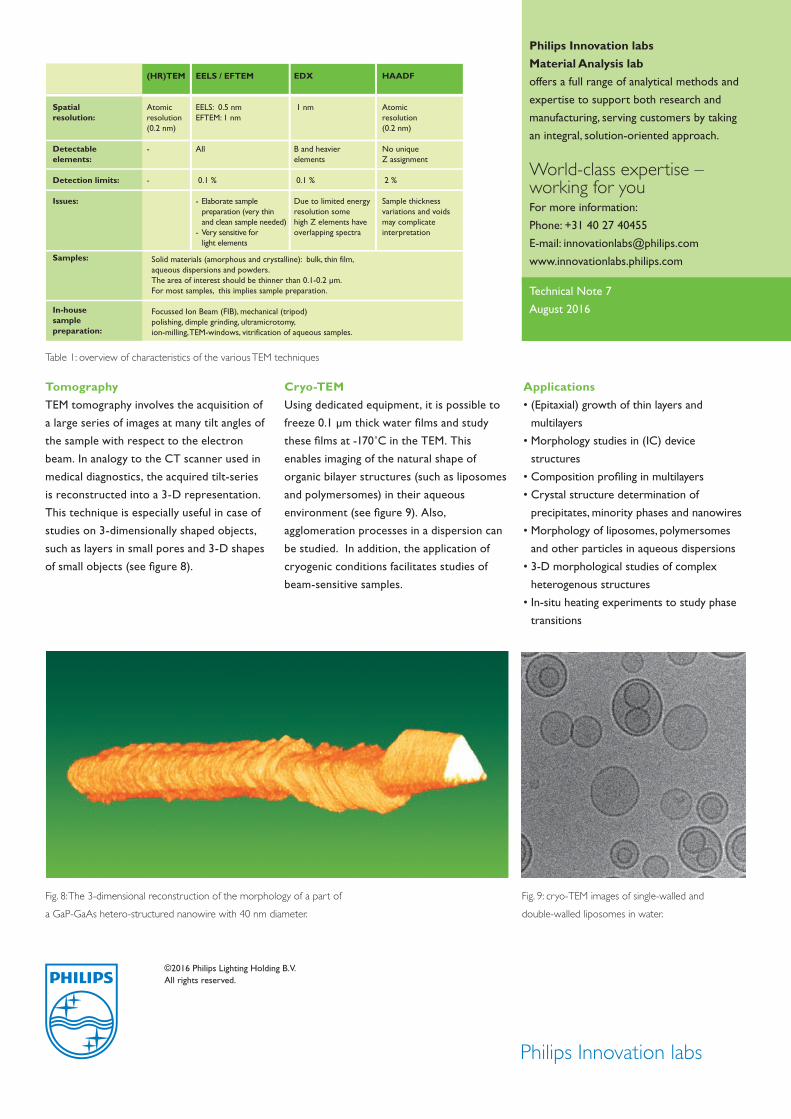
Tomography
TEM tomography involves the acquisition of
a large series of images at many tilt angles of
the sample with respect to the electron
beam. In analogy to the CT scanner used in
medical diagnostics, the acquired tilt-series
is reconstructed into a 3-D representation.
This technique is especially useful in case of
studies on 3-dimensionally shaped objects,
such as layers in small pores and 3-D shapes
of small objects (see figure 8).
Cryo-TEM
Using dedicated equipment, it is possible to
freeze 0.1 µm thick water films and study
these films at -170˚C in the TEM. This
enables imaging of the natural shape of
organic bilayer structures (such as liposomes
and polymersomes) in their aqueous
environment (see figure 9). Also,
agglomeration processes in a dispersion can
be studied. In addition, the application of
cryogenic conditions facilitates studies of
beam-sensitive samples.
Applications
• (Epitaxial) growth of thin layers and
multilayers
• Morphology studies in (IC) device
structures
• Composition profiling in multilayers
• Crystal structure determination of
precipitates, minority phases and nanowires
• Morphology of liposomes, polymersomes
and other particles in aqueous dispersions
• 3-D morphological studies of complex
heterogenous structures
• In-situ heating experiments to study phase
transitions
(HR)TEM
Atomicresolution(0.2 nm)
-
-
EELS / EFTEM
EELS: 0.5 nmEFTEM: 1 nm
All
0.1 %
- Elaborate sample preparation (very thin and clean sample needed) - Very sensitive for light elements
EDX
1 nm
B and heavierelements
0.1 %
Due to limited energy resolution some high Z elements haveoverlapping spectra
HAADF
Atomicresolution(0.2 nm)
No unique Z assignment 2 %
Sample thicknessvariations and voidsmay complicateinterpretation
Spatialresolution:
Detectableelements:
Detection limits:
Issues:
Samples:
In-housesamplepreparation:
Solid materials (amorphous and crystalline): bulk, thin film,aqueous dispersions and powders. The area of interest should be thinner than 0.1-0.2 µm. For most samples, this implies sample preparation.
Focussed Ion Beam (FIB), mechanical (tripod)polishing, dimple grinding, ultramicrotomy, ion-milling, TEM-windows, vitrification of aqueous samples.
Table 1: overview of characteristics of the various TEM techniques
Fig. 8: The 3-dimensional reconstruction of the morphology of a part of
a GaP-GaAs hetero-structured nanowire with 40 nm diameter.
Fig. 9: cryo-TEM images of single-walled and
double-walled liposomes in water.
Philips Innovation labs