TRANSISTORS, HIGH POWER, PNP BASED ON TYPE 2N5153 …
22
TRANSISTORS, HIGH POWER, PNP BASED ON TYPE 2N5153 ESCC Detail Specification No. 5204/002 Issue 5 March 2013 Document Custodian: European Space Agency – see https://escies.org Page 1 of 22
Transcript of TRANSISTORS, HIGH POWER, PNP BASED ON TYPE 2N5153 …

TRANSISTORS, HIGH POWER, PNP
BASED ON TYPE 2N5153
ESCC Detail Specification No. 5204/002
Issue 5 March 2013
Document Custodian: European Space Agency – see https://escies.org
Page 1 of 22

ESCC Detail Specification
No. 5204/002
PAGE 2
ISSUE 5
LEGAL DISCLAIMER AND COPYRIGHT
European Space Agency, Copyright © 2013, All rights reserved.
The European Space Agency disclaims any liability or responsibility, to any person or entity, with respect to any loss or damage caused, or alleged to be caused, directly by the use and application of this ESCC publication.
This publication, without prior permission of the European Space Agency and provided it is not used for a commercial purpose, may be:
− copied in whole, in any medium, without alteration or modification. − copied in part, in any medium, provided that the ESCC document identification, comprising
the ESCC symbol, document number and document issue, is removed.
ESCC Detail Specification
No. 5204/002
PAGE 3
ISSUE 5
DOCUMENTATION CHANGE NOTICE
(Refer to https://escies.org for ESCC DCR content)
DCR No. CHANGE DESCRIPTION
757, 776 Specification upissued to incorporate editorial and technical changes per DCR.
Specification converted into MSWord. Changes in presentation are possible.

ESCC Detail Specification
No. 5204/002
PAGE 4
ISSUE 5
TABLE OF CONTENTS
1 GENERAL 6
1.1 SCOPE 6
1.2 APPLICABLE DOCUMENTS 6
1.3 TERMS, DEFINITIONS, ABBREVIATIONS, SYMBOLS AND UNITS 6
1.4 THE ESCC COMPONENT NUMBER AND COMPONENT TYPE VARIANTS 6
1.4.1 The ESCC Component Number 6
1.4.2 Component Type Variants 7
1.5 MAXIMUM RATINGS 7
1.6 HANDLING PRECAUTIONS 9
1.7 PHYSICAL DIMENSIONS AND TERMINAL IDENTIFICATION 10
1.7.1 Metal Can Package (TO-39) - 3 lead 10
1.7.2 Metal Flange Mount Package (TO-257) - 3 lead 11
1.7.3 Surface Mount Package (SMD.5) - 3 terminal 12
1.8 FUNCTIONAL DIAGRAM 13
1.9 MATERIALS AND FINISHES 14
2 REQUIREMENTS 14
2.1 GENERAL 14
2.1.1 Deviations from the Generic Specification 14
2.1.1.1 Deviation from Qualification and Periodic Tests - Chart F4 14
2.2 MARKING 14
2.3 TERMINAL STRENGTH 14
2.4 VERIFICATION OF SAFE OPERATING AREA 15
2.5 ELECTRICAL MEASUREMENTS AT ROOM, HIGH AND LOW TEMPERATURES 15
2.5.1 Room Temperature Electrical Measurements 15
2.5.2 High and Low Temperatures Electrical Measurements 18
2.6 PARAMETER DRIFT VALUES 18
2.7 INTERMEDIATE AND END-POINT ELECTRICAL MEASUREMENTS 18
2.8 HIGH TEMPERATURE REVERSE BIAS BURN-IN CONDITIONS 19
2.9 POWER BURN-IN CONDITIONS 19
2.9.1 Power Burn-in Conditions (TO-39) 19
2.9.2 Power Burn-in Conditions (TO-257 and SMD.5) 20
2.10 OPERATING LIFE CONDITIONS 20
2.11 TOTAL DOSE RADIATION TESTING 20
2.11.1 Bias Conditions and Total Dose Level for Total dose Radiation Testing 20
2.11.2 Electrical Measurements for Radiation Testing 20
ESCC Detail Specification
No. 5204/002
PAGE 5
ISSUE 5
APPENDIX ‘A’ 22

ESCC Detail Specification
No. 5204/002
PAGE 6
ISSUE 5
1 GENERAL
1.1 SCOPE This specification details the ratings, physical and electrical characteristics and test and inspection data for the component type variants and/or the range of components specified below. It supplements the requirements of, and shall be read in conjunction with, the ESCC Generic Specification listed under Applicable Documents.
1.2 APPLICABLE DOCUMENTS The following documents form part of this specification and shall be read in conjunction with it:
(a) ESCC Generic Specification No. 5000 (b) MIL-STD-750, Test Methods and Procedures for Semiconductor Devices
1.3 TERMS, DEFINITIONS, ABBREVIATIONS, SYMBOLS AND UNITS For the purpose of this specification, the terms, definitions, abbreviations, symbols and units specified in ESCC Basic Specification No. 21300 shall apply.
1.4 THE ESCC COMPONENT NUMBER AND COMPONENT TYPE VARIANTS
1.4.1 The ESCC Component Number The ESCC Component Number shall be constituted as follows:
Example: 520400201R
• Detail Specification Reference: 5204002 • Component Type Variant Number: 01 (as required) • Total Dose Radiation Level Letter: R (as required)

ESCC Detail Specification
No. 5204/002
PAGE 7
ISSUE 5
1.4.2 Component Type Variants
The component type variants applicable to this specification are as follows:
Variant Number
Based on Type Case Lead/Terminal Material and Finish
Weight max g
Total Dose Radiation Level
Letter
01 2N5153 TO-39 D2 1.5 R [100kRAD(Si)]
02 2N5153 TO-39 D3 or D4 1.5 R [100kRAD(Si)]
03 2N5153 TO-39 D7 1.5 R [100kRAD(Si)]
04 2N5153 TO-257 H2 5 R [100kRAD(Si)]
05 2N5153 TO-257 H4 5 R [100kRAD(Si)]
06 2N5153 SMD.5 Q14 2 R [100kRAD(Si)]
07 2N5153 SMD.5 Q14 2 R [100kRAD(Si)]
The lead/terminal material and finish shall be in accordance with the requirements of ESCC Basic Specification No. 23500.
Total dose radiation level letters are defined in ESCC Basic Specification No. 22900. If an alternative radiation test level is specified in the Purchase Order, the letter shall be changed accordingly.
1.5 MAXIMUM RATINGS The maximum ratings shall not be exceeded at any time during use or storage.
Maximum ratings shall only be exceeded during testing to the extent specified in this specification and when stipulated in Test Methods and Procedures of the ESCC Generic Specification.
Characteristics Symbols Maximum Ratings Unit Remarks
Collector-Base Voltage VCBO -100 V Over Top
Collector-Emitter Voltage VCEO -80 V Over Top Note 5
Emitter-Base Voltage VEBO -5.5 V Over Top
Collector Current IC -5 A Continuous Note 5

ESCC Detail Specification
No. 5204/002
PAGE 8
ISSUE 5
Characteristics Symbols Maximum Ratings Unit Remarks
Power Dissipation For TO-39 For TO-257 and SMD.5
Ptot1
1
3.3
W
At Tamb ≤ +25oC
Note 1
For TO-39 For TO-257 and SMD.5
Ptot2 10 35
W At Tcase ≤ +25oC Note 1
Thermal Resistance, Junction-to-Ambient For TO-39 For TO-257 and SMD.5
Rth(j-a)
175 53
oC/W
Thermal Resistance, Junction-to-Case For TO-39 For TO-257 and SMD.5
Rth(j-c)
17.5 5
oC/W
Operating Temperature Range Top -65 to +200 oC Note 2
Storage Temperature Range Tstg -65 to +200 oC Note 2
Soldering Temperature For TO-39 and TO-257 For SMD.5
Tsol +260 +245
oC Note 3 Note 4
NOTES: 1. For Tamb or Tcase > +25oC, derate linearly to 0W at +200oC. 2. For Variants with tin-lead plating or hot solder dip lead finish all testing, and any handling,
performed at Tamb > +125oC shall be carried out in a 100% inert atmosphere. 3. Duration 10 seconds maximum at a distance of not less than 1.5mm from the device body and
the same lead shall not be resoldered until 3 minutes have elapsed. 4. Duration 5 seconds maximum and the same package shall not be resoldered until 3 minutes
have elapsed. 5. Safe Operating Area applies as follows:

ESCC Detail Specification
No. 5204/002
PAGE 9
ISSUE 5
Maximum Safe Operating Area Graph
1.6 HANDLING PRECAUTIONS The TO-257 package contains Beryllium Oxide (BeO) and therefore it must not be ground, machined, sandblasted or subjected to any mechanical operation which will produce dust. The case must not be subjected to any chemical process (e.g. etching) which will produce fumes.

ESCC Detail Specification
No. 5204/002
PAGE 10
ISSUE 5
1.7 PHYSICAL DIMENSIONS AND TERMINAL IDENTIFICATION
1.7.1 Metal Can Package (TO-39) - 3 lead
Symbols Dimensions mm
Notes Min Max
Øa 4.83 5.35
A 6 6.6
Øb 0.4 0.533 2, 3
Øb2 0.4 0.483 2, 3
ØD 8.31 9.4
ØD1 7.75 8.51
h 0.229 3.18
j 0.71 0.864
k 0.737 1.14 4
L 12.7 19 2
L1 - 1.27 2, 3
L2 6.35 - 2, 3
P 2.54 - 5
Q - - 6
α 45o BSC 1, 7
β 90o BSC 1
NOTES: 1. Terminal identification is specified by reference to the tab position where Lead 1 = emitter,
Lead 2 = base and Lead 3 = collector.
ESCC Detail Specification
No. 5204/002
PAGE 11
ISSUE 5
2. Applies to all leads. 3. Øb2 applies between L1 and L2. Øb applies between L1 and 12.7mm from the seating plane.
Diameter is uncontrolled within L1 and beyond 12.7mm from the seating plane. 4. Measured from the maximum diameter of the actual device. 5. This zone is controlled for automatic handling. The variation in actual diameter within this zone
shall not exceed 0.254mm. 6. The details of outline in this zone are optional. 7. Measured from the tab centreline.
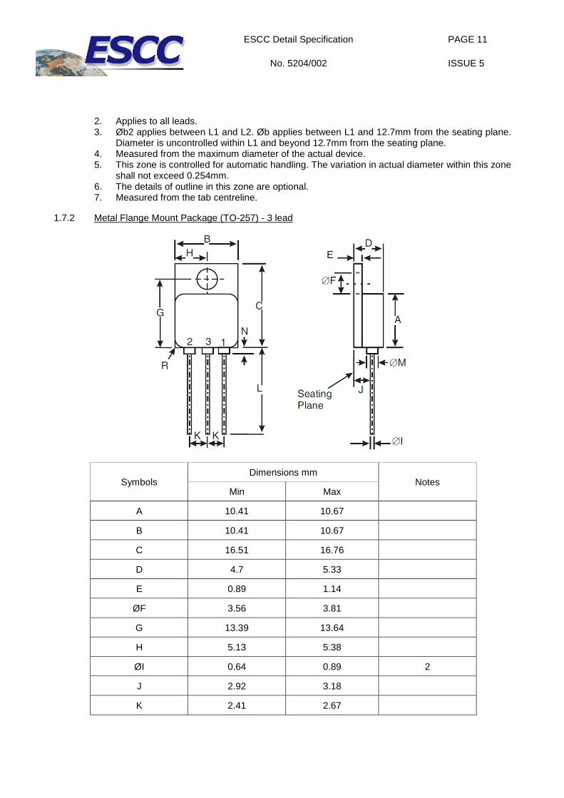
1.7.2 Metal Flange Mount Package (TO-257) - 3 lead
Symbols Dimensions mm
Notes Min Max
A 10.41 10.67
B 10.41 10.67
C 16.51 16.76
D 4.7 5.33
E 0.89 1.14
ØF 3.56 3.81
G 13.39 13.64
H 5.13 5.38
ØI 0.64 0.89 2
J 2.92 3.18
K 2.41 2.67

ESCC Detail Specification
No. 5204/002
PAGE 12
ISSUE 5
Symbols Dimensions mm
Notes Min Max
L 15.24 16.51
ØM 2.29 Typical 2
N - 0.71 2
R 1.65 Typical 3
NOTES: 1. Terminal identification is specified by the components geometry where Lead 1 = emitter, Lead
2 = base and Lead 3 = collector. 2. Applies to all leads. 3. Radius of body corner, 4 places.
1.7.3 Surface Mount Package (SMD.5) - 3 terminal
Symbols Dimensions mm
Notes Min Max
A 2.84 3.15
A1 0.25 0.51
b 7.13 7.39
b1 5.58 5.84
b2 2.28 2.54 2
b3 2.92 3.18 2
D 10.03 10.28
D1 0.76 - 2
ESCC Detail Specification
No. 5204/002
PAGE 13
ISSUE 5
Symbols Dimensions mm
Notes Min Max
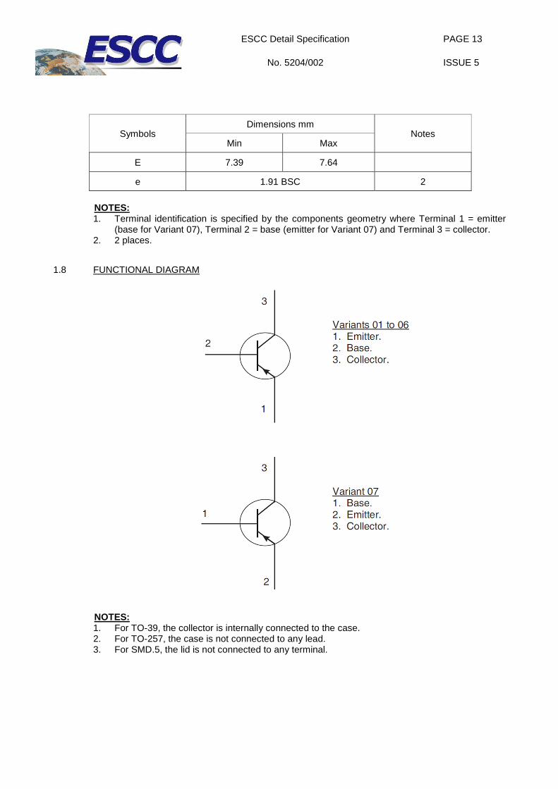
E 7.39 7.64
e 1.91 BSC 2
NOTES: 1. Terminal identification is specified by the components geometry where Terminal 1 = emitter
(base for Variant 07), Terminal 2 = base (emitter for Variant 07) and Terminal 3 = collector. 2. 2 places.
1.8 FUNCTIONAL DIAGRAM
NOTES: 1. For TO-39, the collector is internally connected to the case. 2. For TO-257, the case is not connected to any lead. 3. For SMD.5, the lid is not connected to any terminal.
ESCC Detail Specification
No. 5204/002
PAGE 14
ISSUE 5
1.9 MATERIALS AND FINISHES
Materials and finishes shall be as follows:
(a) Case For the metal can package the case shall be hermetically sealed and have a metal body with hard glass seals. For the metal flange mount package the case shall be hermetically sealed and have a metal body. The leads pass through ceramic eyelets brazed into the frame and the lid shall be welded. For the surface mount package the case shall be hermetically sealed and have a ceramic body with a Kovar lid.
(b) Leads/Terminals As specified in Component Type Variants.
2 REQUIREMENTS
2.1 GENERAL The complete requirements for procurement of the components specified herein are as stated in this specification and the ESCC Generic Specification. Permitted deviations from the Generic Specification, applicable to this specification only, are listed below.
Permitted deviations from the Generic Specification and this Detail Specification, formally agreed with specific Manufacturers on the basis that the alternative requirements are equivalent to the ESCC requirement and do not affect the component’s reliability, are listed in the appendices attached to this specification.
2.1.1 Deviations from the Generic Specification
2.1.1.1 Deviation from Qualification and Periodic Tests - Chart F4 For SMD.5, Terminal Strength is not applicable.
2.2 MARKING The marking shall be in accordance with the requirements of ESCC Basic Specification No. 21700 and as follows.
The information to be marked on the component shall be:
(a) The ESCC qualified components symbol (for ESCC qualified components only). (b) The ESCC Component Number. (c) Traceability information. (d) Warning sign for Beryllium Oxide (TO-257 only)
2.3 TERMINAL STRENGTH The test conditions for terminal strength, tested as specified in the ESCC Generic Specification, shall be as follows:
For TO-39, Test Condition: E, lead fatigue.
For TO-257, Test Condition: A, tension, with an applied force of 10N for a duration of 10s.
ESCC Detail Specification
No. 5204/002
PAGE 15
ISSUE 5
2.4 VERIFICATION OF SAFE OPERATING AREA
The Safe Operating Area shall be verified as specified in the ESCC Generic Specification and Maximum Ratings herein. The test conditions shall be:
Test Method = MIL-STD-750, Method 3051, Continuous DC
Tcase = +25oC
VCE = -18V
IC = -500mA
Operating Time ≤ 50ms
2.5 ELECTRICAL MEASUREMENTS AT ROOM, HIGH AND LOW TEMPERATURES Electrical measurements shall be performed at room, high and low temperatures.
2.5.1 Room Temperature Electrical Measurements The measurements shall be performed at Tamb = +22 ±3oC.
Characteristics Symbols MIL-STD-750 Test Method
Test Conditions Limits Units
Min Max
Collector-Emitter Breakdown Voltage
V(BR)CEO 3011 IC = -100mA Bias condition D Note 1
-80 - V
Collector-Emitter Cut-off Current
ICES 3041 VCE = -60V Bias condition C
- -1 µA
ICEO 3041 VCE = -40V Bias condition D
- -50 µA
Emitter-Base Cut-off Current
IEBO1 3061 VEB = -4V Bias condition D
- -1 µA
IEBO2 3061 VEB = -5.5V Bias condition D
- -1 mA
Forward-Current Transfer Ratio
hFE1 3076 VCE = -5V; IC = -50mA Note 1
50 - -
hFE2 3076 VCE = -5V; IC = -2.5A Note 1
70 200 -
hFE3 3076 VCE = -5V; IC = -5A Note 1
40 - -
ESCC Detail Specification
No. 5204/002
PAGE 16
ISSUE 5
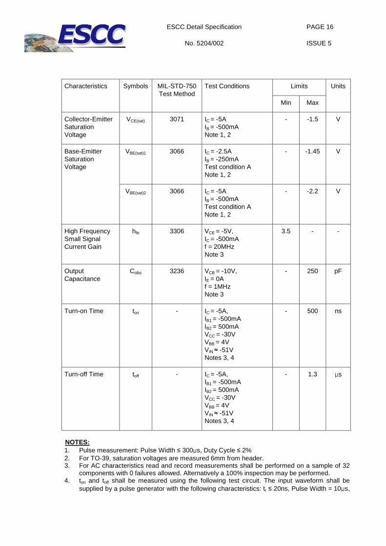
Characteristics Symbols MIL-STD-750 Test Method
Test Conditions Limits Units
Min Max
Collector-Emitter Saturation Voltage
VCE(sat) 3071 IC = -5A IB = -500mA Note 1, 2
- -1.5 V
Base-Emitter Saturation Voltage
VBE(sat)1 3066 IC = -2.5A IB = -250mA Test condition A Note 1, 2
- -1.45 V
VBE(sat)2 3066 IC = -5A IB = -500mA Test condition A Note 1, 2
- -2.2 V
High Frequency Small Signal Current Gain
hfe 3306 VCE = -5V, IC = -500mA f = 20MHz Note 3
3.5 - -
Output Capacitance
Cobo 3236 VCB = -10V, IE = 0A f = 1MHz Note 3
- 250 pF
Turn-on Time ton - IC = -5A, IB1 = -500mA IB2 = 500mA VCC = -30V VBB = 4V VIN ≈ -51V Notes 3, 4
- 500 ns
Turn-off Time toff - IC = -5A, IB1 = -500mA IB2 = 500mA VCC = -30V VBB = 4V VIN ≈ -51V Notes 3, 4
- 1.3 µs
NOTES: 1. Pulse measurement: Pulse Width ≤ 300µs, Duty Cycle ≤ 2% 2. For TO-39, saturation voltages are measured 6mm from header. 3. For AC characteristics read and record measurements shall be performed on a sample of 32
components with 0 failures allowed. Alternatively a 100% inspection may be performed. 4. ton and toff shall be measured using the following test circuit. The input waveform shall be
supplied by a pulse generator with the following characteristics: tr ≤ 20ns, Pulse Width = 10µs,

ESCC Detail Specification
No. 5204/002
PAGE 17
ISSUE 5
Duty Cycle = 1%. The sampling oscilloscope for CH.A and CH.B shall have the characteristics ZIN ≥ 100kΩ, CIN ≤ 12pF and tr ≤ 5ns. Adjustment of VIN shall be made with a suitable current probe to achieve the specified IB1 and IB2 test conditions, where IB1 is the on-state base current and IB2 is the post off-state base current.
ESCC Detail Specification
No. 5204/002
PAGE 18
ISSUE 5
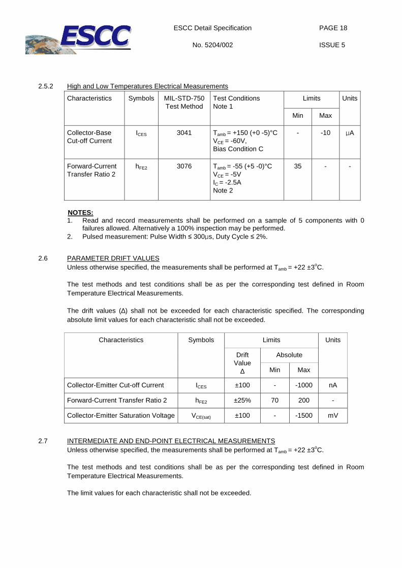
2.5.2 High and Low Temperatures Electrical Measurements
Characteristics Symbols MIL-STD-750 Test Method
Test Conditions Note 1
Limits Units
Min Max
Collector-Base Cut-off Current
ICES 3041 Tamb = +150 (+0 -5)°C VCE = -60V, Bias Condition C
- -10 µA
Forward-Current Transfer Ratio 2
hFE2 3076 Tamb = -55 (+5 -0)°C VCE = -5V IC = -2.5A Note 2
35 - -
NOTES: 1. Read and record measurements shall be performed on a sample of 5 components with 0
failures allowed. Alternatively a 100% inspection may be performed. 2. Pulsed measurement: Pulse Width ≤ 300µs, Duty Cycle ≤ 2%.
2.6 PARAMETER DRIFT VALUES Unless otherwise specified, the measurements shall be performed at Tamb = +22 ±3oC.
The test methods and test conditions shall be as per the corresponding test defined in Room Temperature Electrical Measurements.
The drift values (∆) shall not be exceeded for each characteristic specified. The corresponding absolute limit values for each characteristic shall not be exceeded.
Characteristics
Symbols
Limits Units
Drift Value
∆
Absolute
Min Max
Collector-Emitter Cut-off Current ICES ±100 - -1000 nA
Forward-Current Transfer Ratio 2 hFE2 ±25% 70 200 -
Collector-Emitter Saturation Voltage VCE(sat) ±100 - -1500 mV
2.7 INTERMEDIATE AND END-POINT ELECTRICAL MEASUREMENTS Unless otherwise specified, the measurements shall be performed at Tamb = +22 ±3oC.
The test methods and test conditions shall be as per the corresponding test defined in Room Temperature Electrical Measurements.
The limit values for each characteristic shall not be exceeded.

ESCC Detail Specification
No. 5204/002
PAGE 19
ISSUE 5
Characteristics Symbols Limits Units
Min Max
Collector-Emitter Cut-off Current ICES - -1 µA
Forward-Current Transfer Ratio 2 hFE2 70 200 -
Collector-Emitter Saturation Voltage VCE(sat) - -1.5 V
2.8 HIGH TEMPERATURE REVERSE BIAS BURN-IN CONDITIONS
Characteristics Symbols Conditions Units
Ambient Temperature Tamb +150 oC
Emitter-Base Voltage VEB -4.5 V
Collector-Base Voltage VCB -60 V
Duration t 48 hours
2.9 POWER BURN-IN CONDITIONS
2.9.1 Power Burn-in Conditions (TO-39)
Characteristics Symbols Conditions Units
Ambient Temperature Tamb +20 to +50 (1) oC
Power Dissipation Ptot As per Maximum Ratings. Derate Ptot1 at the chosen Tamb
using the specified Rth(j-a).
W
Collector-Base Voltage VCB -20 V
NOTES: 1. No heat sink nor forced air directly on the device shall be permitted.
ESCC Detail Specification
No. 5204/002
PAGE 20
ISSUE 5
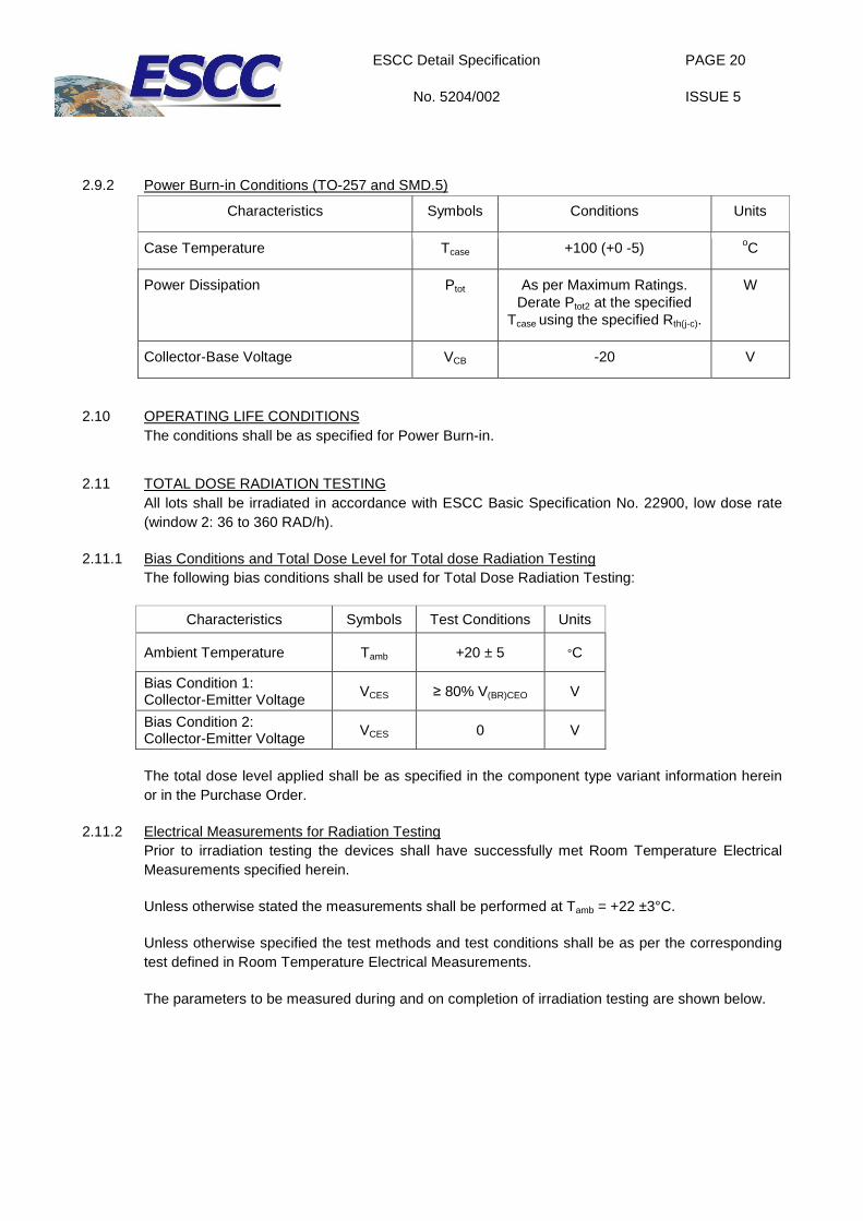
2.9.2 Power Burn-in Conditions (TO-257 and SMD.5)
Characteristics Symbols Conditions Units
Case Temperature Tcase +100 (+0 -5) oC
Power Dissipation Ptot As per Maximum Ratings. Derate Ptot2 at the specified
Tcase using the specified Rth(j-c).
W
Collector-Base Voltage VCB -20 V
2.10 OPERATING LIFE CONDITIONS The conditions shall be as specified for Power Burn-in.
2.11 TOTAL DOSE RADIATION TESTING All lots shall be irradiated in accordance with ESCC Basic Specification No. 22900, low dose rate (window 2: 36 to 360 RAD/h).
2.11.1 Bias Conditions and Total Dose Level for Total dose Radiation Testing The following bias conditions shall be used for Total Dose Radiation Testing:
Characteristics Symbols Test Conditions Units
Ambient Temperature Tamb +20 ± 5 °C
Bias Condition 1: Collector-Emitter Voltage
VCES ≥ 80% V(BR)CEO V
Bias Condition 2: Collector-Emitter Voltage
VCES 0 V
The total dose level applied shall be as specified in the component type variant information herein or in the Purchase Order.
2.11.2 Electrical Measurements for Radiation Testing Prior to irradiation testing the devices shall have successfully met Room Temperature Electrical Measurements specified herein.
Unless otherwise stated the measurements shall be performed at Tamb = +22 ±3°C.
Unless otherwise specified the test methods and test conditions shall be as per the corresponding test defined in Room Temperature Electrical Measurements.
The parameters to be measured during and on completion of irradiation testing are shown below.
ESCC Detail Specification
No. 5204/002
PAGE 21
ISSUE 5
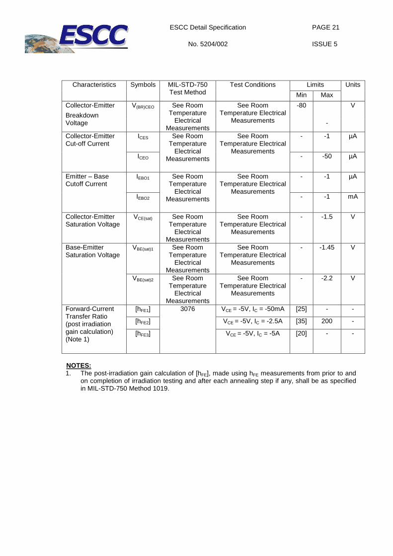
Characteristics Symbols MIL-STD-750
Test Method Test Conditions Limits Units
Min Max
Collector-Emitter V(BR)CEO See Room Temperature
Electrical Measurements
See Room Temperature Electrical
Measurements
-80 V
Breakdown Voltage -
Collector-Emitter Cut-off Current
ICES See Room Temperature
Electrical Measurements
See Room Temperature Electrical
Measurements
- -1 µA
ICEO - -50 µA
Emitter – Base Cutoff Current
IEBO1 See Room Temperature
Electrical Measurements
See Room Temperature Electrical
Measurements
- -1 µA
IEBO2 - -1 mA
Collector-Emitter Saturation Voltage
VCE(sat) See Room Temperature
Electrical Measurements
See Room Temperature Electrical
Measurements
- -1.5 V
Base-Emitter Saturation Voltage
VBE(sat)1 See Room Temperature
Electrical Measurements
See Room Temperature Electrical
Measurements
- -1.45 V
VBE(sat)2 See Room Temperature
Electrical Measurements
See Room Temperature Electrical
Measurements
- -2.2 V
Forward-Current Transfer Ratio (post irradiation gain calculation) (Note 1)
[hFE1] 3076 VCE = -5V, IC = -50mA [25] - -
[hFE2] VCE = -5V, IC = -2.5A [35] 200 -
[hFE3] VCE = -5V, IC = -5A [20] - -
NOTES: 1. The post-irradiation gain calculation of [hFE], made using hFE measurements from prior to and
on completion of irradiation testing and after each annealing step if any, shall be as specified in MIL-STD-750 Method 1019.
ESCC Detail Specification
No. 5204/002
PAGE 22
ISSUE 5
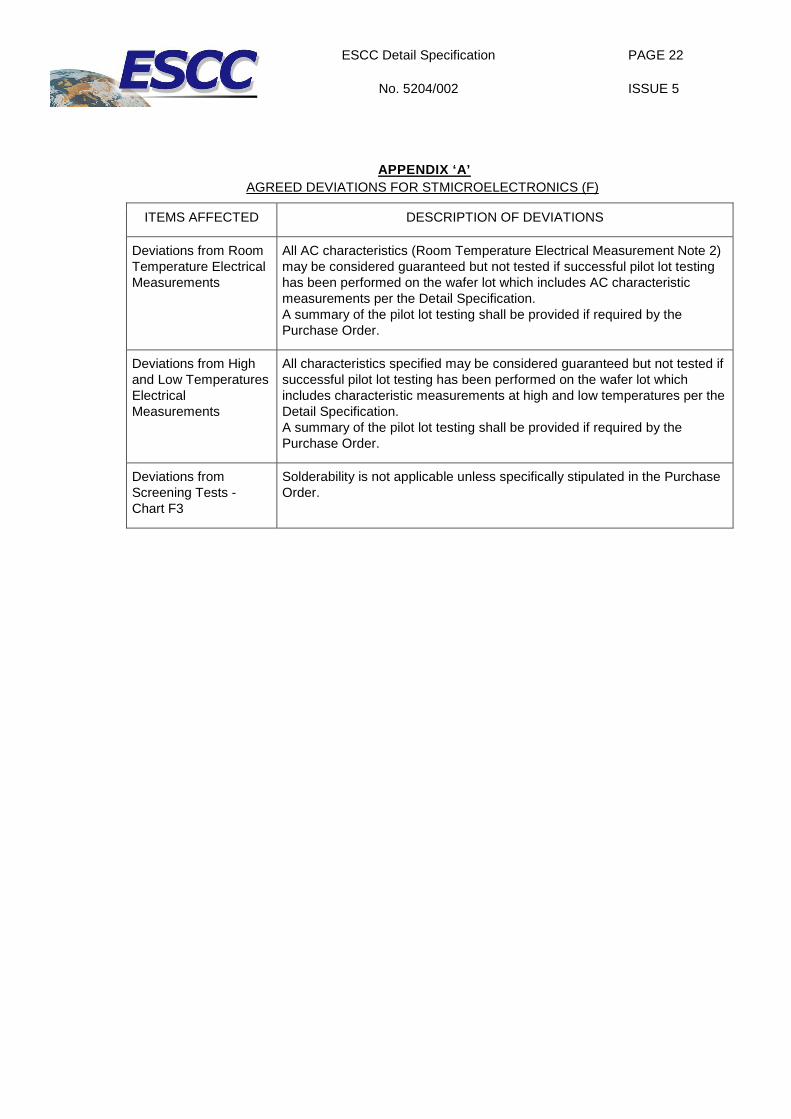
APPENDIX ‘A’
AGREED DEVIATIONS FOR STMICROELECTRONICS (F)
ITEMS AFFECTED DESCRIPTION OF DEVIATIONS
Deviations from Room Temperature Electrical Measurements
All AC characteristics (Room Temperature Electrical Measurement Note 2) may be considered guaranteed but not tested if successful pilot lot testing has been performed on the wafer lot which includes AC characteristic measurements per the Detail Specification. A summary of the pilot lot testing shall be provided if required by the Purchase Order.
Deviations from High and Low Temperatures Electrical Measurements
All characteristics specified may be considered guaranteed but not tested if successful pilot lot testing has been performed on the wafer lot which includes characteristic measurements at high and low temperatures per the Detail Specification. A summary of the pilot lot testing shall be provided if required by the Purchase Order.
Deviations from Screening Tests - Chart F3
Solderability is not applicable unless specifically stipulated in the Purchase Order.


![PEMD12; PUMD12 NPN/PNP resistor-equipped transistors; R1 ... · NPN/PNP resistor-equipped transistors; R1 = 47 k , R2 = 47 k 5. Limiting values Table 6. Limiting values [1] Device](https://static.fdocuments.us/doc/165x107/5f6af1de5184727ecd25db58/pemd12-pumd12-npnpnp-resistor-equipped-transistors-r1-npnpnp-resistor-equipped.jpg)