Transistor Sizing Logical Effort - ece.cmu.eduece322/LECTURES/Lecture7/Lecture7.03.pdf ·...
35
Transistor Sizing Logical Effort Lecture 7 18-322 Fall 2003 Textbook: [5.1, 5.2, 6.1, 6.2-6.2.1]
Transcript of Transistor Sizing Logical Effort - ece.cmu.eduece322/LECTURES/Lecture7/Lecture7.03.pdf ·...

Transistor Sizing Logical Effort
Lecture 718-322 Fall 2003
Textbook: [5.1, 5.2, 6.1, 6.2-6.2.1]
2
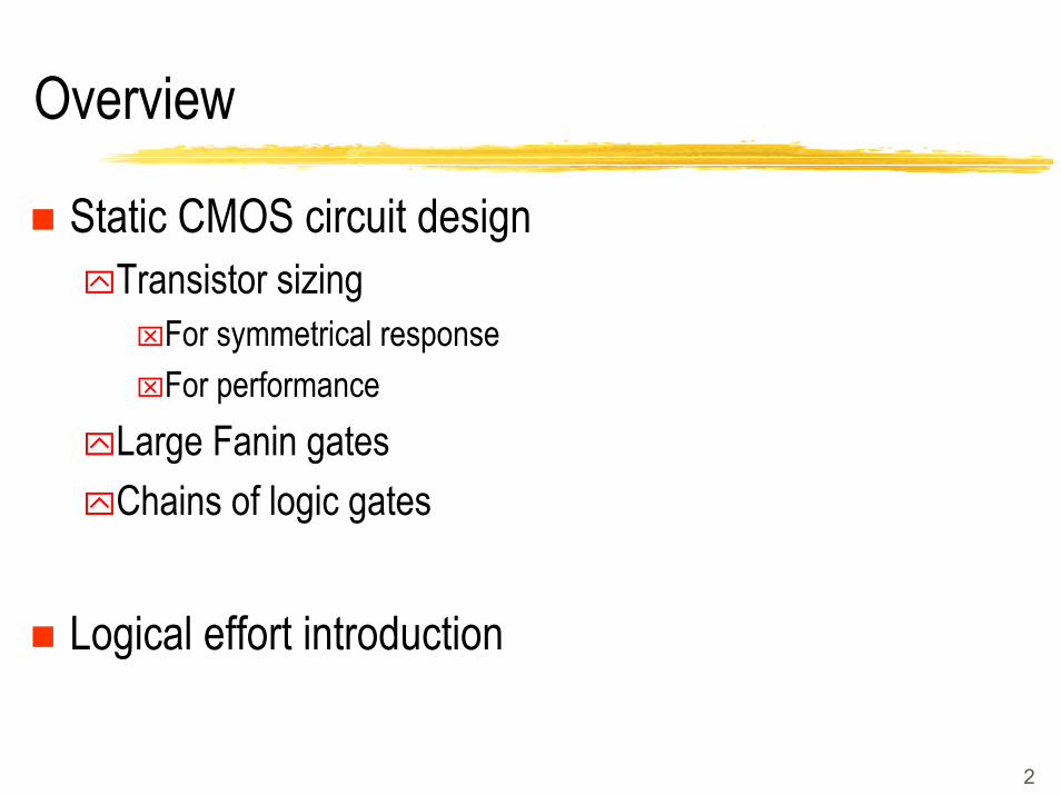
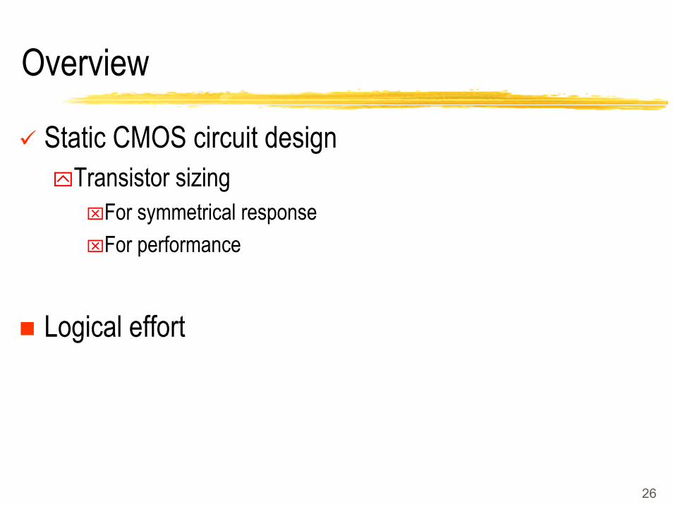
Overview
Static CMOS circuit designTransistor sizing For symmetrical responseFor performance
Large Fanin gatesChains of logic gates
Logical effort introduction

Transistors Everywhere…
Node centric perspective
•Focus on devices and their properties (today)
Network centric perspective
•Focus on interconnects (next lectures)

The MOS Transistor
It is very difficult to derive closed-form solutions that accurately describe modern transistors. For accurate estimations we have Spice. For hand calculations we use simplified models…
Polysilicon Aluminum

What is a Transistor?
−=
WL
)V(VCµ1R
TnGSoxnn Increasing W decreases the
resistance which allows more current to flow!Cox = εox/tox oxide capacitance [F/cm2]
=
=
LWk
LWCµβ '
noxnn device transconductance [A/V2]
(WL) CC oxG = gate capacitance [F]
VGS ≥VT
RonS D
Switch!|VGS|
MOS TransistorG
S D

What is Different Between nFET and pFET?
)V(Vβ1R
TnDDnn −
=n
oxnn LWCµβ
=
3)(2typically Krp
n =µµ
)V(Vβ1R
TpDDpp
−=
poxpp L
WCµβ
=
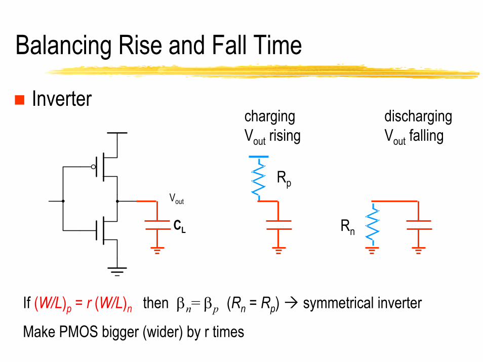
Balancing Rise and Fall Time
InverterchargingVout rising
dischargingVout falling
Vout
Rp
CL Rn
If (W/L)p = r (W/L)n then βn= βp (Rn = Rp) symmetrical inverter
Make PMOS bigger (wider) by r times

FET Sizing and the Unit Transistor
L
W
Source Drain
2W
The electrical characteristics of transistors determine the switching speed of a circuit
Need to select the aspect ratios (W/L)n and (W/L)p of every FET in the circuit
Define the unit transistor (R1, C1)L/Wmin -> highest resistance (needs scaling)R2 = R1/2 and C2 = 2C1 Separate nFET and pFET unit transistorsUnit devices are not restricted ti individual transistors (see next example)
L
L
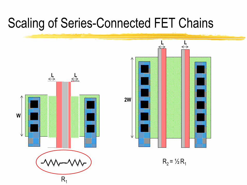
Scaling of Series-Connected FET ChainsL L
2W
R2 = ½ R1
LL
W
R1
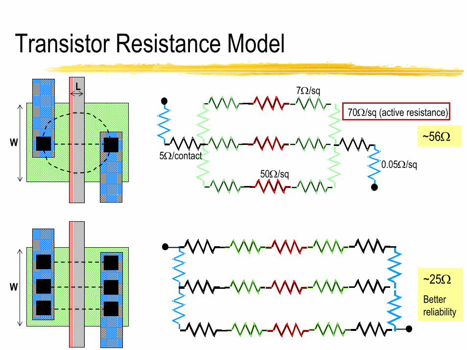
Transistor Resistance ModelL 7Ω/sq
W
W
5Ω/contact
50Ω/sq
70Ω/sq (active resistance)
~56Ω
0.05Ω/sq
~25Ω Better reliability
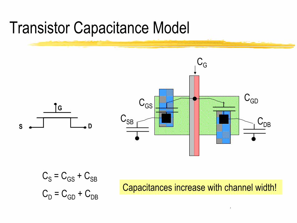
Transistor Capacitance Model
CG
CSB CDB
CGDCGSG
S D
CS = CGS + CSB
CD = CGD + CDBCapacitances increase with channel width!

Inverter Propagation Delay
2W
W
Rp
Rn
CL
Vout
50%
Vin
Voutt
t
• WP = 2WN (symmetrical design)•approx. equal resistances Rn = Rp• approx. equal rise and fall delays
• tp ~ 1/(β VDD) CL -> minimize load, increase width of the driving transistor, increase VDD???
tpf tpr
tpf = ln2 (Rn CL) = 0.69 (Rn CL)
tpr = ln2 (Rp CL)
tp = ½ (tpf + tpr)
Vin Vout
CL
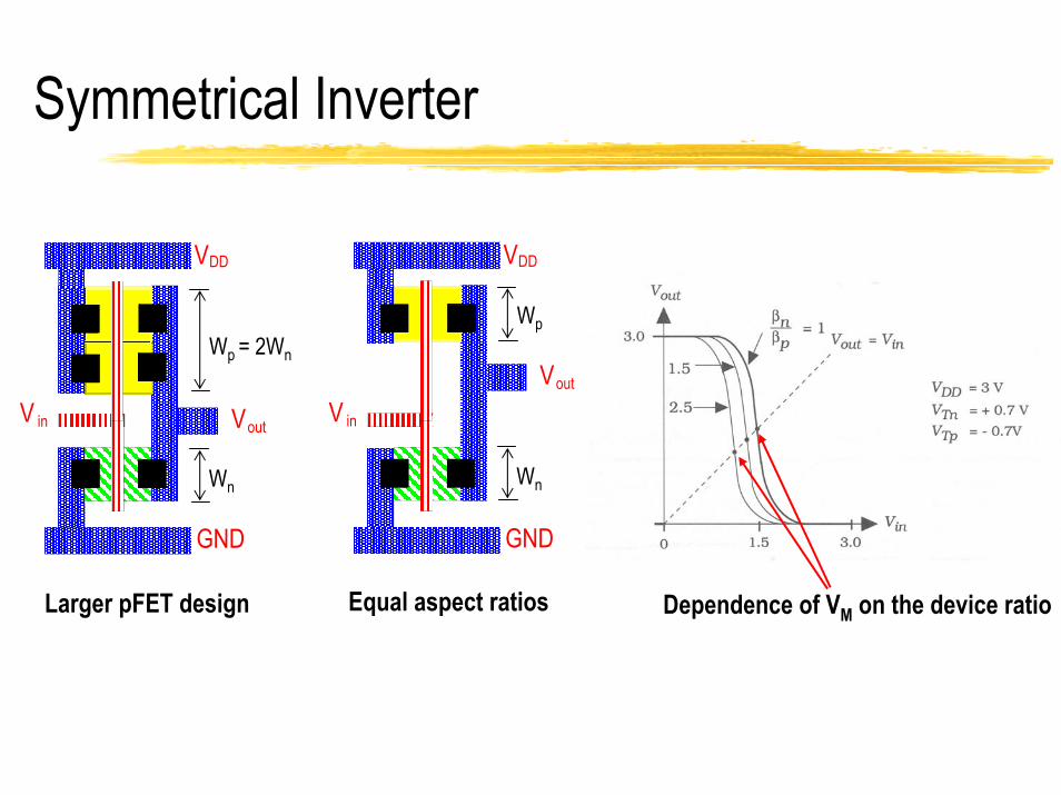
Symmetrical Inverter
V in
Vout
VDD
GND
Wn
Wp
Equal aspect ratiosLarger pFET design
V in Vout
VDD
GND
Wn
Wp = 2Wn
Dependence of VM on the device ratio

Propagation Delay Analysis - The Switch Model
VDDV DDVDD
C L
F C L
CL
F
F
RpRp Rp Rp
Rp
Rn
Rn
Rn Rn Rn
AA
A
AA
A
B B
B
B
(a) Inverter (b) 2-input NAND (c) 2-input NORtp = 0.69 R on C L
(assuming that C L dominates!)
= RON

Analysis of Propagation Delay
VDD
CL
F
Rp Rp
Rn
RnA
A B
B
2-input NAND
1. Assume Rn=Rp= resistance of minimumsized NMOS inverter
2. Determine “Worst Case Input” transition(Delay depends on input values)
3. Example: tpLH for 2input NAND- Worst case when only ONE PMOS Pulls
up the output node- For 2 PMOS devices in parallel, the
resistance is lower
= 0.69RpCLtpLH
4. Example: tpHL for 2input NAND- Worst case : TWO NMOS in series
tpHL = 0.69(2Rn)CL

Transistor Sizing: NAND2
VDD
CL
F
A
A B
B
2
2
1 1
½ + ½
W/L = 2/1
Focus on worst-case
Input Dependent
Here it is assumed that Rp = Rn

Designing for Worst-Case
V DD
AB
C
D
DA
B C
12
22
6
612
12
F
V DD
AB
C
D
DA
B C1
2
22
2
24
4
F
½ + ½
¼ + ¼ ½ + ½
(Wp = 3Wn assumed) Here it is assumed that Rp = Rn

Equivalent Inverter
VDD
A B
A
B
C
Cout
3L
W
L
L
L
W
βseries = βn /3CL
tseries = k -----------------(βn /3) VDD
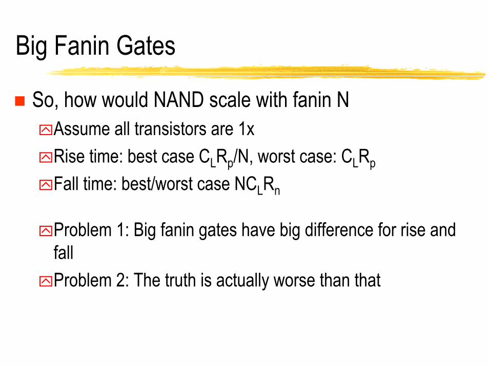
Big Fanin Gates
So, how would NAND scale with fanin NAssume all transistors are 1xRise time: best case CLRp/N, worst case: CLRp
Fall time: best/worst case NCLRn
Problem 1: Big fanin gates have big difference for rise and fallProblem 2: The truth is actually worse than that

The Truth about Transistor Chains
Series Transistors add series resistanceSeries Transistors also add Capacitance
We’ll talk about estimating delay of distributed RC on ThursdayResult: Quadratic, not linear relationship of delay and fanin

tp as a function of Fan-In
VDD
A B
A
B
C
D
C D
1 3 5 7 9fan-in
0.0
1.0
2.0
3.0
4.0
t p (n
sec)
tpHL
tp
tpLHlinear
quadratic
AVOID LARGE FAN-IN GATES! (Typically not more than FI < 4)

Chains of Gates
Making W/L bigger decreases RonDecreases tHL or tLH
But wait! Doesn’t increased W increase capacitance
50%
Vin
Vout
t
t

The Big Trade-off
Making a gate bigger increases it output driveBut also increases its input capacitance
Making this bigger, may make this rise time faster
But it makes this slower because it has to drive more load

How to Optimize?
1
2
W
2W2WCn
WCn
5 Cn
Delay ~ 3 W Cn * Rn + 5Cn * Rn / W
How to optimize?

Summary
Switching delays increase with the external loadThe layout geometries affect the transient response of logic gatesSwitching delays increase with the fan-inIncreasing the “drive” of a gate increases the load to be driven by the previous gate
26
Overview
Static CMOS circuit designTransistor sizing For symmetrical responseFor performance
Logical effort

Logical Effort
A way of thinking about delay in MOS circuits. It seeks to determine quickly a circuit’s maximum possible speed and how to achieve it.
Book: “Logical effort: Designing fast CMOS Circuits” by I. Sutherland, B. Sproull and D. Harris
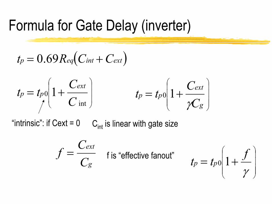
Formula for Gate Delay (inverter)
( )extinteqp CCRt += 69.0
+=int
0 1CCtt ext
pp
+=g
extpp
CCttγ
10
“intrinsic”: if Cext = 0 Cint is linear with gate size
g
ext
CCf =
+=γftt pp 10
f is “effective fanout”
Definitions
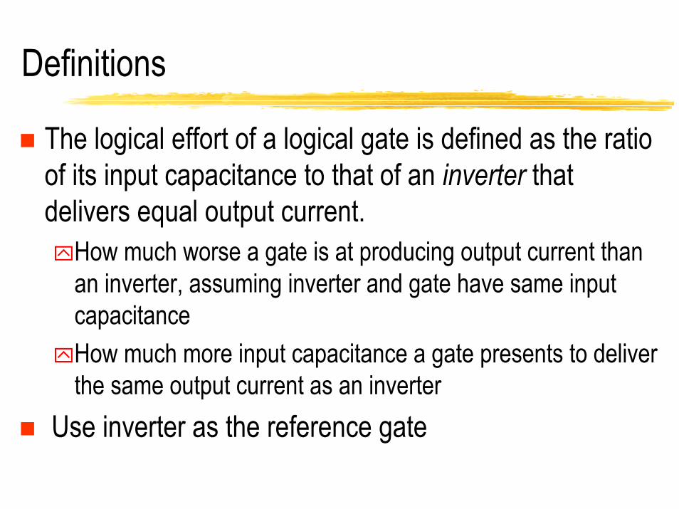
The logical effort of a logical gate is defined as the ratio of its input capacitance to that of an inverter that delivers equal output current.
How much worse a gate is at producing output current than an inverter, assuming inverter and gate have same input capacitanceHow much more input capacitance a gate presents to deliver the same output current as an inverter
Use inverter as the reference gate

Delay Formula for Complex Gates
+=γgfptt pp 0
+=γftt pp 10
g is logical effort
124XOR
7/35/3NOR
5/34/3NAND
1INV
3 inp2 inp1 inpGate
Assume PMOS 2x widerthan NMOS in inverter gates
Rise time == Fall time
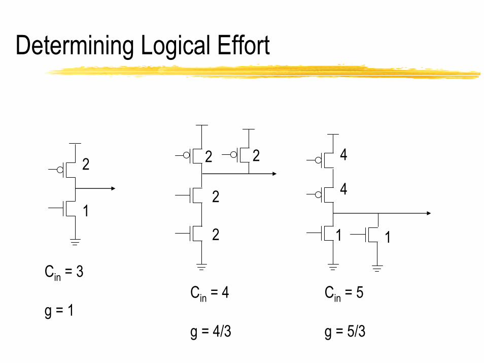
Determining Logical Effort
2
12
2
2 2
4
11
4
Cin = 3
g = 1Cin = 4
g = 4/3
Cin = 5
g = 5/3

Delay thru a Path of Gates
∑ +==
N
i
iiipp
fgptt1
0γ
to Optimize:
NNgfgfgf === ...2211

Logical Effort (cont’d)
Type of efforts- logical path effort (G = Πgi)- electrical path effort (F = Cout/Cin)- branching effort (B = Πbi)
Path effort - H = GFB

Optimization
N-stage logic networkIdea: The path delay is least when each stage in the path bears the same stage effort
hi = gifi = (H)1/N
Main result: minimum delay achievable along a pathD = N (H)1/N + P (where P = ∑pi)Cini = (1/f ) gi Couti (used for transistor sizing!)
The method of logical effort achieves an approximate optimum!

Example
A C y z BC
124XOR
7/35/3NOR
5/34/3NAND
1INV
3 inp2 inp1 inpGate
G = (4/3)3 = 2.37B = 1F = C/C = 1
H = 2.37D = 3(2.37)1/3 + 3(2pinv) = 10 delay units (min delay)
f = (2.37)1/3 = 4/3 (this is the stage effort)z = C (4/3) / (4/3) = Cy = z (4/3) / (4/3) = C (all 3 gates should have the same input capacitance)
4pinvXOR
npinvn-NOR
npinvn-NAND
Pinv= 1Inv
PGate