Transistor Selection and Design of a VHF DC-DC Power … · Transistor Selection and Design of a...
11
IEEE TRANSACTIONS ON POWER ELECTRONICS, VOL. 23, NO. 1,JANUARY 2008 27 Transistor Selection and Design of a VHF DC-DC Power Converter James R. Warren, III, Kathryn Anne Rosowski, and David J. Perreault, Senior Member, IEEE Abstract—This paper explores the design and performance of dc-dc power converters operating in the very high frequency (VHF, 30–300 MHz) range. Methods are presented for assessment and comparison of device losses in VHF operation under soft switching and soft gating conditions. These methods are applied to the devel- opment of a 2 W resonant boost converter operating at a switching frequency of 30 MHz. Design of the power stage, resonant gate drive, and control circuitry are treated in detail, and experimental results demonstrating the performance of the converter are pre- sented. Index Terms—Class E inverter, multiresonant converter, ON-OFF control, resonant converter, resonant gating, zero-voltage switching. I. INTRODUCTION T HE COST, SIZE, and performance of dc-dc power con- verters are heavily dependent on the required size of pas- sive components such as inductors and capacitors. The sizes of passive components often dominate over the switching devices and control circuits, constraining power density. Likewise, the achievable converter transient performance (essentially, the rate at which the converter can adapt its operating condition) is lim- ited by the energy stored in the passive components. Because required component values and energy storage decrease as fre- quency increases [1], there is a motivation to operate switching power converters at as high a frequency as possible commensu- rate with practical constraints such as efficiency. Important frequency-dependent device loss mechanisms include switching loss and gating loss. Zero-voltage switching (e.g., [2]–[12]) can be used to mitigate the voltage/current overlap and capacitive discharge losses associated with device switching. Similarly, soft (resonant) gating [3], [13]–[20] can be employed to reduce the loss associated with charging and discharging MOS device gates. Used together, these techniques enable dramatic increases in the achievable switching frequen- cies of dc-dc converters [3], [16]–[20]. This document explores the design of dc-dc converters op- erating in the VHF frequency range (30–300 MHz). Section II presents a method for evaluating transistors and selecting oper- ating frequencies for class-E-based power converters employing sinusoidal resonant gating. Section III applies this approach to Manuscript received July 20, 2006; revised February 13, 2007. Recom- mended for publication by Associate Editor D. Maksimovic. J. R. Warren, III and D. J. Perreault are with the Laboratory for Electro- magnetic and Electronic Systems, Massachusetts Institute of Technology, Cam- bridge, MA 02139 USA (e-mail: [email protected]; [email protected]). K. A. Rosowski is with Cornell University, Ithaca NY 14853 USA. Color versions of one or more of the figures in this paper are available online at http://ieeexplore.ieee.org. Digital Object Identifier 10.1109/TPEL.2007.911773 Fig. 1. Class E inverter topology [21], [22]. is an RF choke, while the re- maining components are selected as described in [21], [22]. This topology pro- vides zero voltage switching which allows for high frequency operation. the design of a resonant boost converter operating at 30 MHz. Design of the power stage, resonant gate drive, and control cir- cuitry are treated in detail. Section IV presents a summary of the experimental evaluation of this converter and a comparison to the performance of a commercially available alternative. It is demonstrated that small size and fast transient performance are achieved with the proposed approach. Finally, Section V con- cludes the paper. II. TRANSISTOR EVALUATION The performance of power converters operating in the VHF range depends greatly on the characteristics of the power semi- conductor devices. In this section, methods are introduced for assessment and comparison of MOS devices in VHF operation under soft switching and soft gating conditions. These com- parisons are made on the basis of their calculated performance (especially efficiency) in the well-known class E RF inverter topology of Fig. 1 [21], [22]. Device performance in this topology is a useful metric because closed-form expressions are available for it [18], [22], and the underlying loss mecha- nisms remain the same in other circuit topologies. Performance of a given device will differ in other topologies (and may be considerably better), but the relative performance of different devices is likely to remain unchanged. 1 As such, the following derivations apply specifically to the class E topology of Fig. 1, but it is reasonable to utilize the results for transistor evaluation purposes. As a basic measure of device merit, device loss is normalized to ideal output power as a function of switching frequency . The device with the highest frequency capability for a given allowed efficiency penalty may be considered the best device. Normalized device loss may be calculated in terms of device parameters, providing a simple evaluation of device merit as a function of frequency. Alternatively, one may compute the lowest loss device for a given desired power and frequency. This evaluation metric is developed in the following subsections. 1 Note that the detailed loss equations may be different even in other class E topologies [23], [24]. 0885-8993/$25.00 © 2007 IEEE
-
Upload
nguyenthuy -
Category
Documents
-
view
223 -
download
0
Transcript of Transistor Selection and Design of a VHF DC-DC Power … · Transistor Selection and Design of a...

IEEE TRANSACTIONS ON POWER ELECTRONICS, VOL. 23, NO. 1, JANUARY 2008 27
Transistor Selection and Design of a VHF DC-DCPower Converter
James R. Warren, III, Kathryn Anne Rosowski, and David J. Perreault, Senior Member, IEEE
Abstract—This paper explores the design and performance ofdc-dc power converters operating in the very high frequency (VHF,30–300 MHz) range. Methods are presented for assessment andcomparison of device losses in VHF operation under soft switchingand soft gating conditions. These methods are applied to the devel-opment of a 2 W resonant boost converter operating at a switchingfrequency of 30 MHz. Design of the power stage, resonant gatedrive, and control circuitry are treated in detail, and experimentalresults demonstrating the performance of the converter are pre-sented.
Index Terms—Class E inverter, multiresonant converter,ON-OFF control, resonant converter, resonant gating, zero-voltageswitching.
I. INTRODUCTION
THE COST, SIZE, and performance of dc-dc power con-verters are heavily dependent on the required size of pas-
sive components such as inductors and capacitors. The sizes ofpassive components often dominate over the switching devicesand control circuits, constraining power density. Likewise, theachievable converter transient performance (essentially, the rateat which the converter can adapt its operating condition) is lim-ited by the energy stored in the passive components. Becauserequired component values and energy storage decrease as fre-quency increases [1], there is a motivation to operate switchingpower converters at as high a frequency as possible commensu-rate with practical constraints such as efficiency.
Important frequency-dependent device loss mechanismsinclude switching loss and gating loss. Zero-voltage switching(e.g., [2]–[12]) can be used to mitigate the voltage/currentoverlap and capacitive discharge losses associated with deviceswitching. Similarly, soft (resonant) gating [3], [13]–[20] canbe employed to reduce the loss associated with charging anddischarging MOS device gates. Used together, these techniquesenable dramatic increases in the achievable switching frequen-cies of dc-dc converters [3], [16]–[20].
This document explores the design of dc-dc converters op-erating in the VHF frequency range (30–300 MHz). Section IIpresents a method for evaluating transistors and selecting oper-ating frequencies for class-E-based power converters employingsinusoidal resonant gating. Section III applies this approach to
Manuscript received July 20, 2006; revised February 13, 2007. Recom-mended for publication by Associate Editor D. Maksimovic.
J. R. Warren, III and D. J. Perreault are with the Laboratory for Electro-magnetic and Electronic Systems, Massachusetts Institute of Technology, Cam-bridge, MA 02139 USA (e-mail: [email protected]; [email protected]).
K. A. Rosowski is with Cornell University, Ithaca NY 14853 USA.Color versions of one or more of the figures in this paper are available online
at http://ieeexplore.ieee.org.Digital Object Identifier 10.1109/TPEL.2007.911773
Fig. 1. Class E inverter topology [21], [22]. L is an RF choke, while the re-maining components are selected as described in [21], [22]. This topology pro-vides zero voltage switching which allows for high frequency operation.
the design of a resonant boost converter operating at 30 MHz.Design of the power stage, resonant gate drive, and control cir-cuitry are treated in detail. Section IV presents a summary ofthe experimental evaluation of this converter and a comparisonto the performance of a commercially available alternative. It isdemonstrated that small size and fast transient performance areachieved with the proposed approach. Finally, Section V con-cludes the paper.
II. TRANSISTOR EVALUATION
The performance of power converters operating in the VHFrange depends greatly on the characteristics of the power semi-conductor devices. In this section, methods are introduced forassessment and comparison of MOS devices in VHF operationunder soft switching and soft gating conditions. These com-parisons are made on the basis of their calculated performance(especially efficiency) in the well-known class E RF invertertopology of Fig. 1 [21], [22]. Device performance in thistopology is a useful metric because closed-form expressionsare available for it [18], [22], and the underlying loss mecha-nisms remain the same in other circuit topologies. Performanceof a given device will differ in other topologies (and may beconsiderably better), but the relative performance of differentdevices is likely to remain unchanged.1 As such, the followingderivations apply specifically to the class E topology of Fig. 1,but it is reasonable to utilize the results for transistor evaluationpurposes.
As a basic measure of device merit, device loss is normalizedto ideal output power as a function of switching frequency .The device with the highest frequency capability for a givenallowed efficiency penalty may be considered the best device.Normalized device loss may be calculated in terms of deviceparameters, providing a simple evaluation of device merit asa function of frequency. Alternatively, one may compute thelowest loss device for a given desired power and frequency. Thisevaluation metric is developed in the following subsections.
1Note that the detailed loss equations may be different even in other class Etopologies [23], [24].
0885-8993/$25.00 © 2007 IEEE

28 IEEE TRANSACTIONS ON POWER ELECTRONICS, VOL. 23, NO. 1, JANUARY 2008
A. Approximate Class E Operating Characteristics
1) Output Power: Starting from the design equations in [22]and neglecting losses, the input or output power of a class Einverter of Fig. 1 with high loaded Q can be approximated as[18]
(1)
where is power in W, is switching frequency in Hz, is dcinput voltage in V, and is the total capacitance in parallel withthe switch, measured in Farads. Note that of the switchingdevice should be included as part of , with evaluated at adevice voltage of to best model the effect of the non-linear device capacitance on circuit operation. Since the peakdevice voltage reaches approximately 3.6 times the dc inputvoltage, a reasonable approximation is to require a device break-down voltage (e.g., for a MOSFET) of [22].
A further consequence of the power relation in (1) is that thereis a minimum achievable output power for a converter using thistopology under class E operation at a given frequency, obtainedwhen comprises only the device output capacitance
(2)
For a specified output power and input voltage this translatesinto a maximum switching frequency guideline for a classE design
(3)
Frequencies higher than may be used if the converterpower delivered is controlled by means such as adjustmentof the input voltage or by cell modulation [25]. However, itis desirable to match the maximum converter output (at themaximum permissible voltage) to the power output specifi-cation. For purposes of device to device comparison, fixingan output power and determining provides a metric forevaluating switching devices for high frequency applications. Adevice with a higher will allow for reducing the numericalvalues and sizes of passive components in the class E converter,increasing power density relative to a switching device with alower .
2) Losses: The frequency limitations of practical devices de-pend directly on the loss mechanisms. Because the class E in-verter ideally provides zero voltage switching at both transi-tions, there is no capacitive discharge loss at switch turn ON.Moreover, the voltage/current overlap loss at switch turn OFF
can be neglected as it is small compared to other loss compo-nents. The dominant losses, considered here, are device conduc-tion loss and gating loss.
For a MOSFET, the device conduction loss normalized to in-verter power above can be approximated as [18], [22]
(4)
where is the device on-state resistance in , and theother values are as defined above.2
We consider gating loss for a MOSFET in the case where asinusoidal current drive is used to charge and discharge the gate(soft gating). This may be realized with a number of resonantdrive strategies (see, e.g., [3], [16], [18], and Section III-B), andleads to lower loss levels than hard-switched gating when therequired switching time is much longer than the gate time con-stant . Power dissipation due to gating loss,normalized to inverter power , may be computed as
(5)
where is the input capacitance, is the gate resistance,and is the magnitude of the sinusoidal voltage swing atthe gate (e.g., neglecting Miller effect, with the ac voltage swingbeing about a desired dc value such as the MOSFET thresholdvoltage .) should be selected large enough to fullyenhance the device during the “on” time, without exceeding thegate voltage rating. Note that lower gate drive losses are possiblewith other waveforms (e.g., “constant current” charge and dis-charge of the gate, resulting in a trapezoidal gate voltage [19],[20]) but are less simple to realize, and so are not further con-sidered here.
B. Semiconductor Device Evaluation
Here the above operating characteristics are applied to eval-uate devices for VHF power conversion. Evaluation is basedon computing the fractional power loss introducedby the semiconductor switch in a class E inverter as a functionof frequency. For a given allowed fractional loss (e.g., 0.1 for10% power loss in the transistor) this approach reveals an upperbound on operating frequency for a specific device in a class Econverter. When comparing devices, a device having a higheroperating frequency limit may be considered more desirable.The switching frequency limit may be significantly higher inother converter topologies, but the relative performance of dif-ferent devices is likely to remain unchanged.
Two variants of this evaluation procedure are introduced. Thefirst variant is based on selecting an optimal output power foreach candidate frequency to maximize efficiency with the spec-ified transistor. This is useful for general transistor evaluation.The second variant is based on evaluating the transistor acrossfrequency for a specified output power level (i.e., to meet a de-sired application target). This is useful when comparing transis-tors for a target application.
1) General Transistor Evaluation: To evaluate a transistorfor VHF operation, consider the total normalized power loss inthe transistor
(6)
2In designs where C is mostly or entirely composed of device capacitance,conduction through the lossy device capacitance may also represent a signifi-cant loss mechanism. R , the equivalent resistance of the device output ca-pacitance, is shown in Table III for a number of devices.

WARREN et al.: TRANSISTOR SELECTION AND DESIGN OF A VHF DC-DC POWER CONVERTER 29
Fig. 2. Normalized device loss for the FDN361AN MOSFET versus frequencyfor a class E inverter with sinusoidal gate drive. Conduction loss is a constantindependent of frequency, providing the base level. Gating loss varies with thesquare of frequency as in (5), providing the frequency dependence for the nor-malized device loss.
This is the loss in the transistor (due to gating and conduction)normalized to total system power .
For a given switching frequency there is an operating power(in W) that maximizes efficiency subject to the minimum
power constraint of the class E inverter
(7)
in which is calculated as in (2) and . Plot-ting from (6) where is selected at from(7) at each frequency yields the appropriate transistor loss versusfrequency curve. This curve shows the minimum loss achievablewith the specified transistor (in class E operation) and sinusoidalresonant gate drive as a function of frequency. This result maybe considered a lower bound for what is achievable with avail-able VHF converter topologies.
2) Evaluation for a Target Output Power: To evaluate a giventransistor across frequency for a particular target power level P,one can plot from (6) for this power level and aspecified input voltage . This curve can be usedto select a maximum permissible operating frequency for classE operation based on allowed loss in the transistor. Note thatthe allowable operating frequency for this calculation is onlyfor class E operation with sinusoidal gate drive, and is boundedby the limits of (3). As above, this result may be considered alower bound on the performance achievable across topologiesand operating methods.
As an example of this second variant, consider the evalu-ation of a transistor for application in a 2 W converter with
. (6) can be evaluated as a function of frequency forthe device in order to determine maximum operating frequency.From device to device, this maximum frequency can be usedto rank their relative performance, with the objective of identi-fying the highest frequency possible. must be chosen to
Fig. 3. Normalized device loss for the FDN361AN versus P for a class Einverter with sinusoidal gate drive. Conduction loss varies linearly with P asshown in (4). Gating loss is independent of P , so the normalized gating lossfalls with increasing output power.
ensure the device is fully enhanced at turn on. Fig. 2 illustratesthe performance of the FDN361AN MOSFET identified by theselection metrics as a good device for high frequency.3 From thechart, an operating frequency of 30 MHz was selected for theconverter design described in the following section for a target
. Fig. 3 illustrates the device loss for a gen-eral application at a fixed frequency of 30 MHz as a function ofoutput power. This helps evaluate how close the realized targetapplication is to ideal application for the device at 30 MHz.
III. CONVERTER SPECIFICATION AND DESIGN
A resonant boost converter was designed using the transistorselected in Section II. The converter was designed to meet thefollowing specifications: The input voltage ranges from 3.6 Vto 7.2 V, while the output voltage is to be regulated at 7 V. Theoutput power range is from 1 W to 2 W.
The resonant boost converter is based on a soft gated class Einverter combined with a single diode rectifier operating at 30MHz. This frequency was selected above as the target frequencyfor . The output is regulated using cellmodulation control (also called ON-OFF control or burst modecontrol) [20], [25], [26].
In this control scheme, the converter operates at a fixedswitching frequency and duty ratio. To regulate the powerdelivered to the output, the converter operation is gated ON andOFF over time at a rate that is much slower than the switchingfrequency. By appropriately modulating the fraction of the timethat the converter delivers power (at a modulating frequencyfar below the switching frequency) the output voltage can bemaintained at a desired level.
A significant advantage of this control scheme is that the con-verter only runs at fixed switching frequency and duty ratio,facilitating implementation of soft switching and soft gating.
3A selected list of commercially available devices deemed suitable for highfrequency operation is provided in the Appendix along with some importantdevice parameters.

30 IEEE TRANSACTIONS ON POWER ELECTRONICS, VOL. 23, NO. 1, JANUARY 2008
Fig. 4. Block diagram for 2 W dc-dc converter operating at 30 MHz using cellmodulation control. The dc-dc conversion is accomplished by the class E basedinverter and single diode rectifier. The resonant gate drive circuit provides thedrive signal for the inverter. The cell modulation control turns the converter ON
and OFF over time in order to maintain a regulated output voltage.
TABLE ICOMPONENT VALUES FOR A CLASS E BASED RESONANT BOOST CONVERTER
OPERATING AT 30 MHz USING CELL MODULATION CONTROL. INPUT VOLTAGE
RANGES FROM 3.6 V TO 7.2 V, WITH OUTPUT VOLTAGE REGULATED TO 7 V.OUTPUT POWER RANGES FROM 1 W TO 2 W
Moreover, all of the power stage components can be sized basedon the very high switching frequency, yielding small size andfast transient performance. Only the input and output filter ca-pacitors need be sized for the ripple at the lower modulation fre-quency. The practical implications of this strategy will be pre-sented in Section IV.
A block diagram of the converter is presented in Fig. 4. Thethree main components of the converter are the power stage,resonant gate drive circuit, and the cell modulation control. Thedesign and performance of the individual subsystems follow,including a schematic for each block in Fig. 4. All componentvalues are specified in Table I. Experimental results for the fullconverter are presented in Section IV.
Fig. 5. Schematic of the prototype resonant converter power stage. The con-verter is based on a class E inverter whose tank is parallel loaded with a singlediode rectifier. It is also topologically equivalent to the ZVS multiresonant boostconverter proposed in [27], but utilizes a different control method. Componentvalues are listed in Table I.
A. Power Stage
The power stage of the resonant boost converter can be de-veloped from the class E inverter as follows [18]: The seriesresistive load is transformed to an equivalent resistance in par-allel with the tank capacitor. The resistor is then replaced by aresonant single-diode rectifier (which siphons energy out of thetank), yielding the topology of Fig. 5. The tank may be retunedif needed to account for the nonlinear impact of the diode, suchthat near ZVS is maintained over the input voltage range. A ben-efit of the topology of Fig. 5 is that it absorbs the device parasiticcapacitances to the extent that package inductances are not large(a valid approximation in the developed prototype).
Note that the transformation from a load in series with thetank to a load in parallel with the tank capacitor means that afraction of the total power (equal to ) is transferreddirectly as dc current from the input to the output; this reducesloss as compared to processing all power through ac waveforms.A further advantage of the topology of Fig. 5 is that it absorbsthe parasitic capacitances of both the switch and the diode tothe extent that device package inductances can be ignored. (If
and in Fig. 5 entirely comprise device capacitance, thenthe package inductances can be effectively absorbed into and
as well.)It should also be noted that, component value selection aside,
the circuit of Fig. 5 is topologically equivalent to the ZVS “mul-tiresonant” boost converter of [27]. The principle differences be-tween the design introduced here and the approach elucidated in[27] arise from how the circuit is controlled. Because we focuson operation at fixed switching frequency and duty ratio (withon/off control for regulation) rather than constant-off-time/vari-able-frequency control as in [27], we can employ sinusoidal res-onant gating for efficient operation at VHF frequencies. Like-wise, we need not rely on the switch body diode to preserve ZVSoperation across operating conditions. Finally, the use of ON/OFF
control offers the possibility of greatly improved light-load op-eration.
It should be noted that the concept of a steady state conver-sion ratio (e.g., “ ”) is not relevant for the proposed converterdesign. This is because output power and voltage are controlledby modulating the converter ON and OFF over time, and not byrunning continuously at an operating point that provides the req-uisite conversion ratio or output power.
In developing the power stage, simulations in SPICE werecarried out. Detailed simulation models used in this develop-ment may be found in [18]. Manufacturer-provided models wereused for the semiconductor devices. There has also been greatsuccess in utilizing simple “ideal switch plus drop” models of

WARREN et al.: TRANSISTOR SELECTION AND DESIGN OF A VHF DC-DC POWER CONVERTER 31
Fig. 6. Laboratory measurements of drain to source voltage (V ) waveformsacross the input voltage range 3.6 V to 7.2 V for the converter power stageprototype whose schematic is presented in Fig. 5. The transistor is driven usinga sinusoidal signal provided by a power amplifier with V = 18:03 V.
Fig. 7. Multistage resonant gate drive circuit schematic for class E based dc-dcconverter. A relaxation oscillator provides a fixed frequency and duty ratio drivesignal. Three inverters in parallel form a drive stage for the resonant tank. Theresonant tank also develops a dc offset voltage at the gate, allowing the sinu-soidal drive to be centered closer to V of the switching device. Componentvalues are listed in Table I.
the semiconductor devices, augmented with nonlinear capaci-tances. This approach has also been found to be adequate to fre-quencies in excess of 100 MHz. At the highest frequencies, de-vice package inductance and printed circuit board capacitancealso need to be carefully modeled for high accuracy, along withpassive component parasitics such as capacitor ESR and ESL(e.g., see [17].)
A prototype of the power stage illustrated in Fig. 5 was devel-oped prior to the full system design to validate the power stagebehavior. The transistor was gated with a 30 MHz sinusoidaldrive signal via an external power amplifier. The resultant con-verter was then exercised over the full input voltage range whiledriving a fixed voltage load. Fig. 6 shows the waveforms forthe transistor, demonstrating the ZVS behavior across the inputvoltage range.
B. Resonant Gate Drive
A multistage resonant gate drive circuit was designed to op-erate the power stage transistor. The design combines the fea-tures of a self oscillating resonant driver [3], [16], [20] andthe tapered hard-switched driver designs sometimes found in
Fig. 8. Example laboratory measurements of drain to source voltage (V ) andgate to source (V ) waveforms for V = 7 V for the full converter prototype.The power stage of the converter is that whose schematic is presented in Fig. 5,with the gate drive signal provided by the circuit illustrated in Fig. 7.
Fig. 9. Cell modulation architecture block diagram. The output voltage is com-pared to a reference; the result enables or disable the converter power stage. Theoutput filter capacitor buffers the converter output while the power stage is OFF.
low-power integrated converters [28], [29]. The drive circuit isillustrated in Fig. 7. An example gate drive waveform, , forthe resonant gate drive circuit of the final converter prototype ispresented in Fig. 8. The accompanying drain waveform, , isalso included.
The gate drive circuit is made up of two stages of inverters.The first stage is designed as a low current oscillator source,and the second stage is designed as a higher current drive stage.Simple inverters can be used for the drive current stage as wellas adapted to a relaxation oscillator with relatively few compo-nents.
The first stage of the drive structure was designed to be selfoscillating, eliminating the need for a separate oscillator. Theconverter is controlled by alternately disabling the gate driveand allowing it to run freely.
The second stage consists of three parallel inverters designedto deliver sufficient power to the resonant tank. The invertersare utilized for their suitable current drive capability, as well astheir benefit of eliminating the external circuitry a traditionalpush/pull stage would require to mitigate shoot through. Thisdrive stage has three times the current capacity as the oscillatorstage, taking advantage of a tapered multistage design.
The final component of the gate drive circuit is the resonanttank network which operates resonantly to reduce gate drive
32 IEEE TRANSACTIONS ON POWER ELECTRONICS, VOL. 23, NO. 1, JANUARY 2008
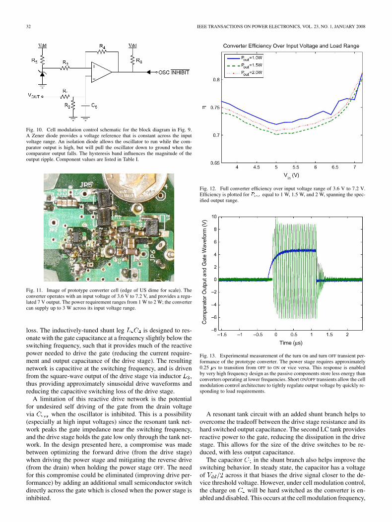
Fig. 10. Cell modulation control schematic for the block diagram in Fig. 9.A Zener diode provides a voltage reference that is constant across the inputvoltage range. An isolation diode allows the oscillator to run while the com-parator output is high, but will pull the oscillator down to ground when thecomparator output falls. The hysteresis band influences the magnitude of theoutput ripple. Component values are listed in Table I.
Fig. 11. Image of prototype converter cell (edge of US dime for scale). Theconverter operates with an input voltage of 3.6 V to 7.2 V, and provides a regu-lated 7 V output. The power requirement ranges from 1 W to 2 W; the convertercan supply up to 3 W across its input voltage range.
loss. The inductively-tuned shunt leg is designed to res-onate with the gate capacitance at a frequency slightly below theswitching frequency, such that it provides much of the reactivepower needed to drive the gate (reducing the current require-ment and output capacitance of the drive stage). The resultingnetwork is capacitive at the switching frequency, and is drivenfrom the square-wave output of the drive stage via inductor ,thus providing approximately sinusoidal drive waveforms andreducing the capacitive switching loss of the drive stage.
A limitation of this reactive drive network is the potentialfor undesired self driving of the gate from the drain voltagevia when the oscillator is inhibited. This is a possibility(especially at high input voltages) since the resonant tank net-work peaks the gate impedance near the switching frequency,and the drive stage holds the gate low only through the tank net-work. In the design presented here, a compromise was madebetween optimizing the forward drive (from the drive stage)when driving the power stage and mitigating the reverse drive(from the drain) when holding the power stage OFF. The needfor this compromise could be eliminated (improving drive per-formance) by adding an additional small semiconductor switchdirectly across the gate which is closed when the power stage isinhibited.
Fig. 12. Full converter efficiency over input voltage range of 3.6 V to 7.2 V.Efficiency is plotted for P equal to 1 W, 1.5 W, and 2 W, spanning the spec-ified output range.
Fig. 13. Experimental measurement of the turn On and turn OFF transient per-formance of the prototype converter. The power stage requires approximately0.25 �s to transition from OFF to ON or vice versa. This response is enabledby very high frequency design as the passive components store less energy thanconverters operating at lower frequencies. Short ON/OFF transients allow the cellmodulation control architecture to tightly regulate output voltage by quickly re-sponding to load requirements.
A resonant tank circuit with an added shunt branch helps toovercome the tradeoff between the drive stage resistance and itshard switched output capacitance. The second LC tank providesreactive power to the gate, reducing the dissipation in the drivestage. This allows for the size of the drive switches to be re-duced, with less output capacitance.
The capacitor in the shunt branch also helps improve theswitching behavior. In steady state, the capacitor has a voltageof across it that biases the drive signal closer to the de-vice threshold voltage. However, under cell modulation control,the charge on will be hard switched as the converter is en-abled and disabled. This occurs at the cell modulation frequency,

WARREN et al.: TRANSISTOR SELECTION AND DESIGN OF A VHF DC-DC POWER CONVERTER 33
Fig. 14. Cell modulation behavior over input voltage and load range. The illustrated waveform is gate voltage of the converter cell on a long time scale to illustratethe cell modulation frequency.
which is significantly lower than the converter frequency of 30MHz. This results in losses of
(8)
where is the inverter rail voltage, and is the rate atwhich the converter is modulated ON and OFF to regulate theoutput.
C. Cell Modulation Control
Fig. 9 contains a simplified block diagram for a cell modu-lated (ON-OFF) control architecture. The main components arethe rf dc-dc converter, an output filter, and a feedback networkto enable or disable the converter. The output filter averages thepower delivered by the converter over time, while the feedbacknetwork enables the converter for an appropriate fraction of timeto meet the load requirement.
A feedback network is needed to monitor the output voltageand provide the modulation (ON/OFF) control signals for the con-verter. The controller schematic is shown in Fig. 10.
A voltage divider network scales the output voltage down forcomparison to a 3 V reference, chosen to be valid over the fullinput voltage range. A hysteresis band is set around the com-parator to provide noise rejection and control the magnitude ofthe output ripple.
The output of the control network is designed to directly en-able or inhibit the converter’s gate drive oscillator. A low outputfrom the comparator pulls the relaxation oscillator input down,disabling the drive circuit, while a high output from the com-parator isolates the comparator from the oscillator, allowing itto run freely.
IV. CONVERTER PERFORMANCE
A prototype dc-dc converter was built using the converter cell,resonant gate circuit, and cell modulation control architecturedescribed in the previous section. The converter is presentedin Fig. 11 along with the edge of a U.S. dime for scale. Theconverter area is approximately 0.75 . The height, includingPCB, is approximately 0.25 in. Full experimental results for thisconverter and a comparison to a commercially available devicefollow.
A. Experimental Results of Full Converter
Efficiency over load and input voltage range is presented inFig. 12. The converter efficiency ranges from 71% to 81% overthe load range of the converter.
The converter cell transient response is illustrated in Fig. 13.Both the cell turn ON and turn OFF time is approximately 0.25in response to the gate driver enable signal. The cell modulationcharacteristics of the converter are illustrated over input voltageand load range in Fig. 14. The modulation frequency range (farbelow the switching frequency of 30 MHz) is enumerated inTable II.
Fig. 15 demonstrates the band limited output voltage ripple aswell as the converter load transient response. At time , theconverter load is stepped from 1 W to 2 W, the entire load rangeof the converter. The cell modulation duty cycle of the converterchanges to meet the load requirement, and the transient responseof the circuit does not exceed the output ripple of the converteroperating in steady state. (The visible noise spike is from theload switching circuit.) The cell modulation control architectureeasily adapts to changing load conditions.

34 IEEE TRANSACTIONS ON POWER ELECTRONICS, VOL. 23, NO. 1, JANUARY 2008
TABLE IICELL MODULATION FREQUENCIES FOR A 2 WATT RESONANT BOOST
CONVERTER. THE MODULATION FREQUENCIES ARE PRESENTED AT THE FOUR
CORNER POINTS OF INPUT VOLTAGE RANGE AND LOAD. INPUT VOLTAGE
RANGES FROM 3.6 V TO 7.2 V, AND THE LOAD RANGES FROM 1 W TO 2 W
Fig. 15. AC output ripple measurement for the cell modulated converter pro-totype around the regulated dc output voltage, 7 V. The power stage is turnedON during the positive slope portions, and shut down during the negative por-tions. The 30 MHz switching ripple is highly undersampled in this photographleaving the modulation frequency component visible. This figure also illustratesthe transient response to a load step from 1 W to 2 W at time t = 0. The spikeseen at t = 0 is from the load switching circuit.
B. Relative Performance of a Commercial Converter
A commercial boost converter design was used as a bench-mark for comparison to the new design. The LM7231Y boostconverter from National Semiconductor was selected for com-parison. It is an integrated switch boost converter operating at aswitching frequency of 600 kHz. An evaluation board from themanufacturer, having similar output capacitance (10 ) to theVHF design and configured to match the 7 V output specifica-tion of the prototype, was used for the comparison. The evalua-tion board uses a 4.7 boost inductor.
The prototype converter was compared to the LM7231Y interms of ripple performance and load transient behavior. Circuitarea was comparable, though further integration work on theprototype could reduce its size while the LM7231Y is already afully integrated part except for external passive components.
The ripple performance of the LM7231Y is presented inFig. 16. It is appropriate to compare this to Fig. 15 for theprototype converter. The static switching ripple of the conven-tional converter is approximately one third that due to the VHFdesign. This is not surprising, given that the two designs use
Fig. 16. National Semiconductor LM7231Y ripple response measurementinput voltage is 5 V and output voltage is configured for 7 V. The load is 1 W.The top graph presents the full bandwidth measurement, and the bottom graphpresents the measurement with a 20 MHz measurement bandwidth.
Fig. 17. National Semiconductor LM7231Y load transient response. The mea-surement is ac coupled and bandlimited to 20 MHz. The load steps from 2 W to1 W, resulting in a transient response of up to 50% overshoot.
similar levels of output capacitance and the highest modulationfrequency of the VHF design is roughly one third the switchingfrequency of the conventional design.
It is also important to consider the transient performance ofthe two designs. The ac coupled response of the LM7231Y eval-uation board output voltage to a load transient is illustrated inFig. 17. The load is stepped from 2 W to 1 W, resulting in a 3.5volt overshoot and 0.5 volt undershoot around the 7 V operationvoltage.
The main benefit of the resonant boost converter is revealedby comparing Fig. 17 and Fig. 15. The transient response of theVHF resonant boost converter does not even exceed its nominal

WARREN et al.: TRANSISTOR SELECTION AND DESIGN OF A VHF DC-DC POWER CONVERTER 35
TABLE IIIREPRESENTATIVE DEVICES SUITABLE FOR HIGH-FREQUENCY OPERATION UNDER SOFT-SWITCHING AND SOFT-GATING OPERATION.
LISTED PARAMETERS ARE A MIXTURE OF DATASHEET VALUES AND MEASURED PARAMETERS
steady state output voltage ripple. In comparison, the LM7231Yovershoots its operating point by 50%. The cell modulated reso-nant boost converter provides a tightly regulated output voltageover any transient within its load range specification using onlysmall passive components. Achieving a similar level of rippleand transient performance from the conventional design wouldrequire dramatic increases in output capacitance, with commen-surate increases in circuit size.
This comparison underscores an important difference be-tween the proposed approach and conventional low-frequencyPWM designs. In a VHF design with ON/OFF control, the bulkoutput capacitance is selected based on a specified ripple.One way to reduce ripple is to increase the bulk capacitance.Alternatively, however, the modulation ripple of a VHF designcan be reduced without increasing bulk capacitance and withvery little efficiency penalty through the use of low dropout

36 IEEE TRANSACTIONS ON POWER ELECTRONICS, VOL. 23, NO. 1, JANUARY 2008
linear post regulation or active ripple filtering (e.g., [30]–[34]).A conventional converter, by contrast, requires a large bulkcapacitor to meet transient requirements, independent of rippleconsiderations. (Linear post regulation and active filtering arenot typically effective for large-signal transient variations, es-pecially for voltage undershoot.) The reduction in bulk energystorage in the power stage due to VHF operation thus providesdifferent constraints on the design of input and output filterswhich can be of significant advantage in many cases.
V. CONCLUSION
The desire to reduce passive component size and improvedynamic performance of dc-dc converters motivates the devel-opment of designs operating at very high switching frequen-cies. Practical operation at these frequencies requires circuit de-signs, control methods, and semiconductor devices that providelow-loss switching and gating of the devices. This paper ex-plores transistor selection and design of very high frequencydc-dc converters.
Methods for evaluating MOSFET transistors and selectingoperating frequencies for VHF power converters are presented.The selection metrics are for class-E based converters em-ploying sinusoidal resonant gating, but may be expected to beuseful on a qualitative level for a broader range of VHF topolo-gies. These methods are applied to the design of a resonantboost converter operating at 30 MHz using a conventional ver-tical power MOSFET. Design of the power stage, resonant gatedrive, and control circuitry are treated in detail. Experimentalresults demonstrating the performance of the converter are pre-sented along with a comparison to a conventional design. It isshown that the VHF design achieves a combination of size anddynamic performance that is far better than the conventionaldesign.
APPENDIX
This appendix provides a representative list of MOSFETsthat the authors have identified as good candidates for high-fre-quency operation under soft-switching and soft-gating condi-tions. Parameters provided are a mixture of datasheet values andmeasured parameters of sample devices. (Gate resistance in par-ticular is often not provided in datasheets, as it is not of primaryimportance in hard-gated converters.) Table III presents the data.
It should be noted that the authors and their colleagues haveused a subset of the devices listed here to realize designs oper-ating at frequencies up to 110 MHz at tens of Volts and Watts(e.g., [17], [19], [20], and [35]) and up to 30 MHz at hundredsof Volts and Watts (e.g., [36] and [37]). Moreover, additional in-creases in power at a given frequency can be obtained throughthe use of a cellular converter architecture, as described in [16],[25].
REFERENCES
[1] J. Kassakian, M. Schlecht, and G. Verghese, Principles of Power Elec-tron.. New York: Addison-Wesley, 1991.
[2] R. Gutmann, “Application of RF circuit design principles to distributedpower converters,” IEEE Trans. Ind. Electron. Contr. Instrum., vol.IEC127, no. 3, pp. 156–164, Aug. 1980.
[3] W. Bowman, J. Balicki, F. Dickens, R. Honeycutt, W. Nitz, W. Strauss,W. Suiter, and N. Zeisse, “A resonant dc-to-dc converter operating at22 Megahertz,” in Proc. 3rd Annu. IEEE Applied Power Electron. Conf.and Expo. APEC ’88, New Orleans, LA, Feb. 1988, pp. 3–11.
[4] A. F. Goldberg and J. G. Kassakian, “The application of power MOS-FETs at 10 MHz,” in Proc. 16th Annu. IEEE Power Electron. Special-ists Conf., Jun. 1985, pp. 91–100.
[5] R. Goldfarb, “A new non-dissipative load-line shaping technique elim-inates switching stress in bridge converters,” in Proc. Int. Solid-StatePower Electron. Conf. POWERCON, Apr. 1981, vol. D4, pp. 1–6.
[6] R. Redl and N. O. Sokal, “A 14 MHz 100 watt class E resonant con-verter: Principles, design considerations and measured performance,”in Proc. Power Electron. Show and Conf., San Jose, CA, Oct. 1986,vol. 1, pp. 68–77.
[7] R. Redl, B. Molnar, and N. Sokal, “Class E resonant regulated dc/dcpower converters: Analysis of operations and experimental results at1.5 MHz,” IEEE Trans. Power Electron., vol. PE-1, no. 2, pp. 111–120,Apr. 1986.
[8] R. L. Steigerwald, “A comparison of half-bridge resonant convertertopologies,” IEEE Trans. Power Electron., vol. 3, no. 2, pp. 174–182,Apr. 1988.
[9] F. Lee, “High-frequency quasi-resonant converter technologies,” Proc.IEEE, vol. 76, pp. 377–390, Apr. 1988.
[10] G. Hua and F. C. Lee, “An overview of soft-switching techniques forPWM converters,” Euro. Power Electron. Drives J., vol. 3, no. 1, p. 39,Mar. 1993.
[11] K. M. Smith and K. M. Smedley, “Properties and synthesis of passivelossless soft-switching PWM converters,” IEEE Trans. Power Elec-tron., vol. 14, no. 5, pp. 890–899, Sep. 1999.
[12] R. Redl and N. O. Sokal, “A new class-E dc/dc converter family with re-duced parts count: Derivation, topologies, and design considerations,”in Proc. 4th Int. High Frequency Power Conversion Conf., Naples, FL,May 1989, pp. 395–415.
[13] D. Maksimovic, “A MOS gate drive with resonant transitions,” in Proc.22nd Annu. IEEE Power Electron. Specialists Conf., Jun. 1991, pp.527–532.
[14] I. D. de Vries, “A resonant power MOSFET/IGBT gate driver,” inProc. 17th Annu. IEEE Applied Power Electron. Conf., 2002, vol. 1,pp. 179–185.
[15] D. M. Van de Sype, A. P. M. Van den Bossche, J. Maes, and J. A.Melkebeek, “Gate-drive circuit for zero-voltage-switching half- andfull-bridge converters,” IEEE Trans. Ind. Appl., vol. 38, no. 5, pp.1380–1388, Sept./Oct. 2002.
[16] J. M. Rivas, J. Shafran, R. S. Wahby, and D. J. Perreault, “New ar-chitectures for radio-frequency dc/dc power conversion,” IEEE Trans.Power Electron., vol. 21, no. 2, pp. 380–393, Mar. 2006.
[17] D. Jackson, “Design and characterization of a radio-frequency dc/dcpower converter,” M.Eng. thesis, Dept. Elect. Eng. Computer Sci.,Massachusetts Institute of Technology, Cambridge, May 2005.
[18] J. R. Warren, III, “Cell modulated dc/dc converter,” M.Eng. thesis,Dept. Elect. Eng. Computer Sci., Massachusetts Institute of Tech-nology, Cambridge, Aug. 2005.
[19] Y. Han, O. Leitermann, D. A. Jackson, J. M. Rivas, and D. J. Per-reault, “Resistance compression networks for resonant power conver-sion,” IEEE Trans. Power Electron., vol. 22, no. 1, pp. 41–53, Jan. 2007.
[20] J. M. Rivas, D. Jackson, O. Leitermann, A. D. Sagneri, Y. Han, andD. J. Perreault, “Design considerations for radio frequency dc-dc con-verters,” in Proc. IEEE Power Electron. Specialists Conf., Jeju, Korea,Jun. 2006, pp. 2287–2297.
[21] N. O. Sokal and A. D. Sokal, “Class E—A new class of high-efficiencytuned single-ended switching power amplifiers,” IEEE J. Solid-StateCircuits, vol. SC10, no. 3, pp. 168–176, Jun. 1975.
[22] N. O. Sokal, “Class-E RF power amplifiers,” QEX, pp. 9–20, Jan./Feb.2001.
[23] M. Idaware and S. Mori, “Even harmonic resonant class E tuned poweramplifier without RF choke,” Electron. Commu. Jpn., vol. 79, no. 1, pt.1, pp. 22–30, 1996.
[24] A. Grebennikov, “Load network design for class E RF and microwaveamplifiers,” High Frequency Electron., pp. 18–32, Jul. 2004.
[25] J. M. Rivas, J. Shafran, R. S. Wahby, and D. J. Perreault, “New archi-tectures for radio-frequency dc/dc power conversion,” in Proc. IEEEPower Electron. Specialists Conf., Aachen, Germany, Jun. 2004, pp.4074–4084.
[26] Y. S. Lee and Y. C. Cheng, “580 kHz switching regulator using on-offcontrol,” J. Inst. Electron. Radio Eng., vol. 57, no. 5, pp. 221–226,Sep.–Oct. 1987.
[27] W. A. Tabisz and F. C. Lee, “Zero-voltage-switching multi-resonanttechnique—A novel approach to improve performance of high fre-quency quasi-resonant converters,” in Proc. IEEE Power ElectronicSpecialists Conf., Apr. 1988, vol. 1, pp. 9–17.
[28] V. Kursun, S. G. Narendra, V. K. De, and E. G. Friedman,“Low-voltage-swing monolithic dc-dc conversion,” IEEE Trans.Circuits Syst. II: Exp. Briefs, vol. 51, no. 5, pp. 241–248, May 2004.
[29] A. J. Stratakos, S. R. Sanders, and R. W. Brodersen, “Low-voltageCMOS dc-dc converter for a portable battery-operated system,” inProc. 25th Annu. IEEE Power Electron. Specialists Conf., PESC’94,Jun. 1994, vol. 1, pp. 619–626.

WARREN et al.: TRANSISTOR SELECTION AND DESIGN OF A VHF DC-DC POWER CONVERTER 37
[30] M. Zhu, D. J. Perreault, V. Caliskan, T. C. Neugebauer, S. Guttowski,and J. G. Kassakian, “Design and evaluation of feedforward activeripple filters,” IEEE Trans. Power Electron., pp. 276–285, Mar. 2005.
[31] A. Chow and D. Perreault, “Design and evaluation of a hybrid pas-sive/active ripple filter with voltage injection,” IEEE Trans. Aerosp.Electron. Sys., vol. 39, no. 2, pp. 471–480, Apr. 2003.
[32] N. K. Poon, J. C. P. Liu, C. K. Tse, and M. H. Pong, “Techniques forinput ripple current cancellation: Classification and implementation,”IEEE Trans. Power Electron., vol. 15, no. 6, pp. 1144–1152, Nov. 2000.
[33] L. E. LaWhite and M. F. Schlecht, “Techniques for input ripple currentcancellation: Classification and implementation,” IEEE Trans. PowerElectron., vol. PE-2, no. 4, pp. 282–290, Oct. 1987.
[34] J. Walker, “Design of practical and effective active EMI filters,” in Proc.Poweron 11, 1984, vol. I-3, pp. 1–8.
[35] R. C. N. Pilawa-Podgurski, A. D. Sagneri, J. M. Rivas, D. I. Anderson,and D. J. Perreault, “Very high frequency resonant boost converters,” inProc. IEEE Power Electron. Specialists Conf., Orlando, FL, Jun. 2007,pp. 2718–2724.
[36] J. M. Rivas, “Radio-frequency dc-dc power conversion,” Ph.D. dis-sertation, Dept. Elect. Eng. Computer Sci., Massachusetts Institute ofTechnology, Cambridge, August 2006.
[37] J. M. Rivas, Y. Han, O. Leitermann, and D. J. Perreault, “A high-fre-quency resonant inverter topology with low voltage stress,” in Proc.IEEE Power Electron. Specialists Conf., Orlando, FL, Jun. 2007, pp.2705–2717.
James R. Warren, III received the B.S. and M.Eng.degrees from the Massachusetts Institute of Tech-nology, Cambridge, in 2004 and 2005, respectively.
His graduate research was supported by theC. S. Draper Laboratory, Cambridge, through aDraper Fellow position. In 2005, he began workin research and development of electronic systemsfor communications, signal processing, and sensingapplications.
Kathryn Anne Rosowski is working toward thebachelors degree in physics, with a concentration inbiology, at Cornell University, Ithaca, NY.
Her current research interests are in the area of neu-robiology.
David J. Perreault (S’91–M’97–SM’06) receivedthe B.S. degree from Boston University, Boston,MA, in 1989, and the S.M. and Ph.D. degreesfrom the Massachusetts Institute of Technology,Cambridge, MA, in 1991 and 1997, respectively.
In 1997, he joined the MIT Laboratory for Electro-magnetic and Electronic Systems as a PostdoctoralAssociate, and became a Research Scientist in thelaboratory in 1999. In 2001, he joined the MITDepartment of Electrical Engineering and Com-puter Science, where he is presently the Emanuel
E. Landsman Associate Professor of Electrical Engineering and ComputerScience. His research interests include design, manufacturing, and controltechniques for power electronic systems and components, and in their usein a wide range of applications. Dr. Perreault received the Richard M. BassOutstanding Young Power Electron. Engineer Award from the IEEE PowerElectron. Society, an ONR Young Investigator Award, and the SAE Ralph R.Teetor Educational Award, and is co-author of two IEEE prize papers.