
TPS784-Q1 300-mA, High-PSRR Low-Dropout Voltage …
52
TPS784-Q1 300-mA, High-PSRR Low-Dropout Voltage Regulator With High Accuracy and Enable 1 Features • AEC-Q100 qualified for automotive applications: – Temperature grade 1: –40°C to +125°C, T A • Device junction temperature: –40°C to +150°C, T J • Input voltage range: 1.65 V to 6.0 V • Available output voltages: – Adjustable option: 1.2 V to 5.5 V – Fixed options: 0.65 V to 5.0 V • Output accuracy: 0.5% typical, 1.7% maximum • 50-dB PSRR out to 100 kHz • Low I Q : 25 µA (typical) • Ultra-low dropout: – 115 mV (max) at 300 mA (3.3 V OUT ) • Internal 500-µs soft-start time to reduce inrush current • Active output discharge • Functional Safety-Capable – Documentation available to aid functional safety system design • Packages: – 3-mm × 3-mm wettable flank VSON (8) – 5-pin SOT-23 2 Applications • Automotive head units • Hybrid instrument clusters • Telematics control units • DC/DC converters 3 Description The TPS784-Q1 ultra low-dropout regulator (LDO) is a small, low quiescent current LDO that can source 300 mA with excellent line and load transient performance. The low output noise and great PSRR performance make the device suitable to power sensitive analog loads. The TPS784-Q1 is a flexible device for post regulation because this device supports an input voltage range from 1.65 V to 6.0 V and offers an adjustable output range of 1.2 V to 5.5 V. The device also features fixed output voltages from 0.65 V to 5.0 V for powering common voltage rails. The TPS784-Q1 offers foldback current limit to reduce power dissipation during over current condition. The EN input helps with power sequencing requirements of the system. The internal soft-start provides a controlled startup reducing the inrush current allowing for lower input capacitance to be used. The TPS784-Q1 provides an active pulldown circuit to quickly discharge output loads when disabled. Device Information (1) PART NUMBER PACKAGE BODY SIZE (NOM) TPS784-Q1 Wettable flank VSON (8) (2) 3.00 mm × 3.00 mm SOT-23 (5) 2.90 mm × 1.60 mm (1) For all available packages, see the orderable addendum at the end of the data sheet. (2) Preview package. Output Current (A) Dropout Voltage (mV) 0 0.03 0.06 0.09 0.12 0.15 0.18 0.21 0.24 0.27 0.3 0 20 40 60 80 100 120 140 160 180 200 T J 55qC 40qC 0qC 25qC 85qC 125qC 150qC Dropout vs I OUT for 5.0 V Output Current (A) Output Voltage Accuracy (%) 0 0.03 0.06 0.09 0.12 0.15 0.18 0.21 0.24 0.27 0.3 -0.25 -0.2 -0.15 -0.1 -0.05 0 0.05 0.1 0.15 0.2 0.25 T J 55qC 40qC 0qC 25qC 85qC 125qC 150qC Output Accuracy vs I OUT for 5.0 V www.ti.com TPS784-Q1 SBVS387B – FEBRUARY 2020 – REVISED APRIL 2021 Copyright © 2021 Texas Instruments Incorporated Submit Document Feedback 1 Product Folder Links: TPS784-Q1 TPS784-Q1 SBVS387B – FEBRUARY 2020 – REVISED APRIL 2021 An IMPORTANT NOTICE at the end of this data sheet addresses availability, warranty, changes, use in safety-critical applications, intellectual property matters and other important disclaimers. PRODUCTION DATA.
Transcript of TPS784-Q1 300-mA, High-PSRR Low-Dropout Voltage …
TPS784-Q1 300-mA, High-PSRR Low-Dropout Voltage Regulator With High Accuracyand Enable
1 Features• AEC-Q100 qualified for automotive applications:
– Temperature grade 1: –40°C to +125°C, TA• Device junction temperature: –40°C to +150°C, TJ• Input voltage range: 1.65 V to 6.0 V• Available output voltages:
– Adjustable option: 1.2 V to 5.5 V– Fixed options: 0.65 V to 5.0 V
• Output accuracy: 0.5% typical, 1.7% maximum• 50-dB PSRR out to 100 kHz• Low IQ: 25 µA (typical)• Ultra-low dropout:
– 115 mV (max) at 300 mA (3.3 VOUT)• Internal 500-µs soft-start time to reduce inrush
current• Active output discharge• Functional Safety-Capable
– Documentation available to aid functional safetysystem design
• Packages:– 3-mm × 3-mm wettable flank VSON (8)– 5-pin SOT-23
2 Applications• Automotive head units• Hybrid instrument clusters• Telematics control units• DC/DC converters
3 DescriptionThe TPS784-Q1 ultra low-dropout regulator (LDO)is a small, low quiescent current LDO that cansource 300 mA with excellent line and load transientperformance.
The low output noise and great PSRR performancemake the device suitable to power sensitive analogloads. The TPS784-Q1 is a flexible device for postregulation because this device supports an inputvoltage range from 1.65 V to 6.0 V and offers anadjustable output range of 1.2 V to 5.5 V. The devicealso features fixed output voltages from 0.65 V to5.0 V for powering common voltage rails.
The TPS784-Q1 offers foldback current limit to reducepower dissipation during over current condition. TheEN input helps with power sequencing requirementsof the system. The internal soft-start provides acontrolled startup reducing the inrush current allowingfor lower input capacitance to be used.
The TPS784-Q1 provides an active pulldown circuit toquickly discharge output loads when disabled.
Device Information(1)
PART NUMBER PACKAGE BODY SIZE (NOM)
TPS784-Q1Wettable flankVSON (8)(2) 3.00 mm × 3.00 mm
SOT-23 (5) 2.90 mm × 1.60 mm
(1) For all available packages, see the orderable addendum atthe end of the data sheet.
(2) Preview package.
Output Current (A)
Dro
pout V
oltage (
mV
)
0 0.03 0.06 0.09 0.12 0.15 0.18 0.21 0.24 0.27 0.30
20
40
60
80
100
120
140
160
180
200TJ
�55qC�40qC
0qC25qC
85qC125qC
150qC
Dropout vs IOUT for 5.0 VOutput Current (A)
Outp
ut V
oltage A
ccura
cy (
%)
0 0.03 0.06 0.09 0.12 0.15 0.18 0.21 0.24 0.27 0.3-0.25
-0.2
-0.15
-0.1
-0.05
0
0.05
0.1
0.15
0.2
0.25
TJ
�55qC�40qC
0qC25qC
85qC125qC
150qC
Output Accuracy vs IOUT for 5.0 V
www.ti.comTPS784-Q1
SBVS387B – FEBRUARY 2020 – REVISED APRIL 2021
Copyright © 2021 Texas Instruments Incorporated Submit Document Feedback 1
Product Folder Links: TPS784-Q1
TPS784-Q1SBVS387B – FEBRUARY 2020 – REVISED APRIL 2021
An IMPORTANT NOTICE at the end of this data sheet addresses availability, warranty, changes, use in safety-critical applications,intellectual property matters and other important disclaimers. PRODUCTION DATA.

Table of Contents1 Features............................................................................12 Applications..................................................................... 13 Description.......................................................................14 Revision History.............................................................. 25 Pin Configuration and Functions...................................36 Specifications.................................................................. 4
6.1 Absolute Maximum Ratings ....................................... 46.2 ESD Ratings .............................................................. 46.3 Recommended Operating Conditions ........................56.4 Thermal Information ...................................................56.5 Electrical Characteristics ............................................66.6 Typical Characteristics................................................ 8
7 Detailed Description......................................................227.1 Overview................................................................... 227.2 Functional Block Diagrams....................................... 227.3 Feature Description...................................................237.4 Device Functional Modes..........................................26
8 Application and Implementation.................................. 278.1 Application Information............................................. 278.2 Typical Application.................................................... 34
9 Power Supply Recommendations................................3510 Layout...........................................................................36
10.1 Layout Guidelines................................................... 3610.2 Layout Examples.................................................... 37
11 Device and Documentation Support..........................3811.1 Device Support........................................................3811.2 Documentation Support.......................................... 3811.3 Receiving Notification of Documentation Updates.. 3811.4 Support Resources................................................. 3811.5 Trademarks............................................................. 3811.6 Electrostatic Discharge Caution.............................. 3811.7 Glossary.................................................................. 38
12 Mechanical, Packaging, and OrderableInformation.................................................................... 39
4 Revision HistoryNOTE: Page numbers for previous revisions may differ from page numbers in the current version.
Changes from Revision A (November 2020) to Revision B (April 2021) Page• Reworded the VIN conditions to have more clarity on what 1.65 V or whichever is greater applies to.............. 6• Added line item for 1.2 V ≤ VOUT < 1.5 V dropout voltage in the DRB package. ............................................... 6
Changes from Revision * (February 2020) to Revision A (November 2020) Page• Changed document status from advance information to production data.......................................................... 1
TPS784-Q1SBVS387B – FEBRUARY 2020 – REVISED APRIL 2021 www.ti.com
2 Submit Document Feedback Copyright © 2021 Texas Instruments Incorporated
Product Folder Links: TPS784-Q1

5 Pin Configuration and Functions
1IN
2GND
3EN 4 NC
5 OUT
Not to scale
Figure 5-1. DBV Package (Fixed), 5-Pin SOT-23,Top View
Thermal
Pad
1
2
3
8
7
6
OUT
NC
NC
EN
NC
IN
4NC 5 GND
Figure 5-2. DRB Package (Fixed), 8-Pin VSON,Top View
1IN
2GND
3EN 4 FB
5 OUT
Not to scale
Figure 5-3. DBV Package (Adjustable), 5-PinSOT-23, Top View
Thermal
Pad
1
2
3
8
7
6
OUT
FB
NC
EN
NC
IN
4NC 5 GND
Figure 5-4. DRB Package (Adjustable), 8-Pin VSON,Top View
Table 5-1. Pin FunctionsPIN
I/O DESCRIPTIONNAME DBV
(Adjustable)DBV
(Fixed)DRB
(Adjustable)DRB
(Fixed)
EN 3 3 7 7 InputEnable pin. Driving this pin to logic high enables the device; drivingthis pin to logic low disables the device. Do not float this pin. If notused, connect EN to IN.
FB 4 — 2 — Input
Feedback pin. Input to the control-loop error amplifier. This pin isused to set the output voltage of the device with the use of externalresistors. Do not float this pin. For adjustable-voltage version devicesonly
GND 2 2 5 5 — Ground pin. This pin must be connected to ground on the board.
IN 1 1 8 8 Input
Input pin. For best transient response and to minimize inputimpedance, use the recommended value or larger ceramic capacitorfrom IN to ground; see the Recommended Operating Conditionstable. Place the input capacitor as close to the input of the deviceas possible.
NC — 4 3, 4, 6 2, 3, 4, 6 — No connect pin. This pin is not internally connected. Connect toground for best thermal performance or leave floating.
OUT 5 5 1 1 Output
A 0.47-µF or greater effective capacitance is required from OUT toground for stability. For best transient response, use a 1-µF or largerceramic capacitor from OUT to ground. Place the output capacitoras close to output of the device as possible; see the RecommendedOperating Conditions table.
ThermalPad N/A N/A Pad Pad —
The thermal pad is electrically connected to the GND pin. Connectthe thermal pad to a large-area GND plane for improved thermalperformance.
www.ti.comTPS784-Q1
SBVS387B – FEBRUARY 2020 – REVISED APRIL 2021
Copyright © 2021 Texas Instruments Incorporated Submit Document Feedback 3
Product Folder Links: TPS784-Q1

6 Specifications6.1 Absolute Maximum Ratingsover operating free-air temperature range (unless otherwise noted)(1)
MIN MAX UNIT
Voltage
Supply, VIN –0.3 6.5 V
Enable, VEN –0.3 6.5 V
Output, VOUT –0.3 VIN + 0.3(2) V
Feedback, VFB –0.3 2 V
Current Output, IOUT Internally limited
TemperatureOperating junction, TJ –40 150 °C
Storage, Tstg –65 150 °C
(1) Stresses beyond those listed under Absolute Maximum Ratings may cause permanent damage to the device. These are stressratings only, which do not imply functional operation of the device at these or any other conditions beyond those indicated underRecommended Operating Conditions. Exposure to absolute-maximum-rated conditions for extended periods may affect devicereliability.
(2) The absolute maximum rating is VIN + 0.3 V or 6.5 V, whichever is smaller.
6.2 ESD RatingsVALUE UNIT
V(ESD) Electrostatic dischargeHuman-body model (HBM), per AEC Q100-002(1) ±2000
VCharged-device model (CDM), per AEC Q100-011 ±500
(1) AEC Q100-002 indicates that HBM stressing shall be in accordance with the ANSI/ESDA/JEDEC JS-001 specification.
TPS784-Q1SBVS387B – FEBRUARY 2020 – REVISED APRIL 2021 www.ti.com
4 Submit Document Feedback Copyright © 2021 Texas Instruments Incorporated
Product Folder Links: TPS784-Q1

6.3 Recommended Operating Conditionsover operating free-air temperature range (unless otherwise noted)
MIN NOM MAX UNIT
VIN Input voltage 1.65 6.0 V
VOUT Output voltageAdjustable output 1.2 5.5
VFixed output 0.65 5.0
CIN Input capacitor 0.1 1 µF
COUT Output capacitor 1(1) 200 µF
CFF Feed-forward capacitor(2) 0 10 100 nF
IOUT Output current 0 300 mA
COUT,ESR Output capacitor ESR 0.001 1 Ω
VEN Enable voltage 0 6 V
FEN Enable toggle frequency 10 kHz
TJ Junction temperature –40 150 °C
(1) The minimum effective capacitance is 0.47 µF.(2) Feed-forward capacitor is optional and not required for stability.
6.4 Thermal Information
THERMAL METRIC(1)
TPS784-Q1
UNITDRB (VSON) DBV (SOT-23)
8 PINS 5 PINS
RθJA Junction-to-ambient thermal resistance 61.8(2) 170.8(3) °C/W
RθJC(top) Junction-to-case (top) thermal resistance 74.1 93.1 °C/W
RθJB Junction-to-board thermal resistance 34.3 10.2 °C/W
ψJT Junction-to-top characterization parameter 6.2 17.5 °C/W
ψJB Junction-to-board characterization parameter 34.1 40 °C/W
RθJC(bot) Junction-to-case (bottom) thermal resistance 18.1 n/a °C/W
(1) For more information about traditional and new thermal metrics, see the Semiconductor and IC Package Thermal Metrics applicationreport.
(2) The 1s0p RθJA value (based on JEDEC 51-3) is 226.5 ℃/W for the DRB package.(3) The 1s0p RθJA value (based on JEDEC 51-3) is 277.3 ℃/W for the DBV package.
www.ti.comTPS784-Q1
SBVS387B – FEBRUARY 2020 – REVISED APRIL 2021
Copyright © 2021 Texas Instruments Incorporated Submit Document Feedback 5
Product Folder Links: TPS784-Q1

6.5 Electrical Characteristicsat operating temperature range (TJ = –40°C to +150°C), VIN = VOUT(nom) + 0.5 V or 1.65 V (whichever is greater), IOUT =1 mA, VEN = VIN, and CIN = COUT = 1 µF, unless otherwise noted. All typical values at TJ = 25°C.
PARAMETER TEST CONDITIONS MIN TYP MAX UNIT
VIN Input voltage 1.65 6.0 V
VOUT Output voltageAdjustable output 1.2 5.5
VFixed output 0.65 5.0
VOUT Output accuracy(1)
1 mA ≤ IOUT ≤ 300 mA,VOUT(nom) + 0.5 V or 1.65 V(whichever is greater) ≤ VIN ≤6.0 V
TJ = 25°C –0.5 0.5
%–40°C ≤ TJ ≤ 85°C –1 1
–40°C ≤ TJ ≤ 150°C –1.7 1.7
VOUT Line regulation VOUT(nom) + 0.5 V or 1.65 V (whichever is greater) ≤ VIN ≤6.0 V 0.3 mV
VOUT Load regulation 0.1 mA ≤ IOUT ≤ 300 mA–40°C ≤ TJ ≤ 85°C –5 5
mV–40°C ≤ TJ ≤ 150°C –5 10
ΔVOUT
Load transient responsesettling time(2) (3) COUT = 10 µF 10 µs
Load transient responseovershoot, undershoot (3) (5) tR = tF = 1 µs, COUT = 10 µF
IOUT = 90 mA to210 mA –2%
%VOUTIOUT = 210 mA to90 mA 10%
IOUT = 0 mA to300 mA –10%
IGND Ground current
IOUT = 0 mAVOUT(nom) + 0.5 V or 1.65 V(whichever is greater) ≤ VIN ≤6.0 V
TJ = 25°C 15 25 30
µA
–40°C ≤ TJ ≤ 85°C 33
–40°C ≤ TJ ≤ 150°C 40
IOUT = 500 µAVOUT(nom) + 0.5 V or 1.65 V(whichever is greater) ≤ VIN ≤6.0 V
TJ = 25°C 33 43
–40°C ≤ TJ ≤ 85°C 45
–40°C ≤ TJ ≤ 150°C 48
ISHDN Shutdown current
VEN ≤ 0.3 VVOUT(nom) + 0.5 V or 1.65 V(whichever is greater) ≤ VIN ≤6.0 V
TJ = 25°C 0.01 0.05
µA–40°C ≤ TJ ≤ 85°C 0.25
–40°C ≤ TJ ≤ 150°C 3
VFB Feedback voltage Adjustable output only 1.182 1.2 1.218 V
IFB Feedback pin current Adjustable output only –0.05 0.01 0.05 µA
ICL Output current limit VIN = VOUT(nom) + 1 V,VOUT = 0.9 x VOUT(nom) (4) 320 420 mA
ISC Short-circuit current limit VOUT = 0 V 162.5 mA
VDO Dropout voltage IOUT = 300 mA,VOUT = 0.95 x VOUT(nom)
0.65 V ≤ VOUT < 0.8 V 900
mV
0.8 V ≤ VOUT < 1.2 V 775
1.2 V ≤ VOUT < 1.5 V 300
1.5 V ≤ VOUT < 1.8 V 175
1.8 V ≤ VOUT < 2.5 V 140
2.5 V ≤ VOUT ≤ 5.0 V 115
1.2 V ≤ VOUT < 1.5 V,DRB Package only 320
PSRR Power-supply rejection ratio IOUT = 300 mA , VIN =VOUT + 1 V
f = 1 kHz 60
dBf = 100 kHz 45
f = 1 MHz 30
Vn Output noise voltage BW = 10 Hz to 100 kHz, VOUT = 1.2 V 30 µVRMS
VUVLO UVLO thresholdVIN rising 1.32 1.42 1.6
VVIN falling 1.17 1.29 1.42
VUVLO(HYST) UVLO hysteresis VIN hysteresis 130 mV
tSTR Start-up time From EN low-to-high transition to VOUT = VOUT(nom) x 95% 280 500 780 µs
VEN(HI) EN pin logic high voltage 0.85V
VEN(LOW) EN pin logic low voltage 0.425
TPS784-Q1SBVS387B – FEBRUARY 2020 – REVISED APRIL 2021 www.ti.com
6 Submit Document Feedback Copyright © 2021 Texas Instruments Incorporated
Product Folder Links: TPS784-Q1
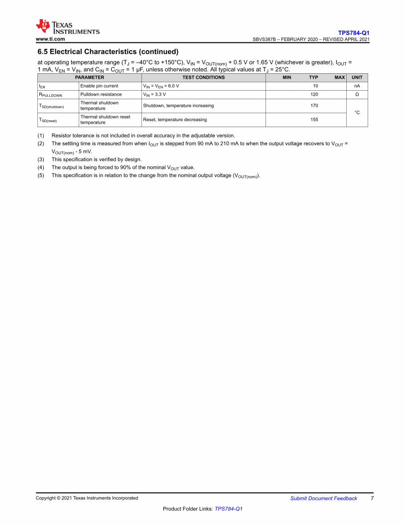
6.5 Electrical Characteristics (continued)at operating temperature range (TJ = –40°C to +150°C), VIN = VOUT(nom) + 0.5 V or 1.65 V (whichever is greater), IOUT =1 mA, VEN = VIN, and CIN = COUT = 1 µF, unless otherwise noted. All typical values at TJ = 25°C.
PARAMETER TEST CONDITIONS MIN TYP MAX UNIT
IEN Enable pin current VIN = VEN = 6.0 V 10 nA
RPULLDOWN Pulldown resistance VIN = 3.3 V 120 Ω
TSD(shutdown)Thermal shutdowntemperature Shutdown, temperature increasing 170
°CTSD(reset)
Thermal shutdown resettemperature Reset, temperature decreasing 155
(1) Resistor tolerance is not included in overall accuracy in the adjustable version.(2) The settling time is measured from when IOUT is stepped from 90 mA to 210 mA to when the output voltage recovers to VOUT =
VOUT(nom) - 5 mV.(3) This specification is verified by design.(4) The output is being forced to 90% of the nominal VOUT value.(5) This specification is in relation to the change from the nominal output voltage (VOUT(nom)).
www.ti.comTPS784-Q1
SBVS387B – FEBRUARY 2020 – REVISED APRIL 2021
Copyright © 2021 Texas Instruments Incorporated Submit Document Feedback 7
Product Folder Links: TPS784-Q1

6.6 Typical Characteristicsat operating temperature TJ = 25°C, IOUT = 1 mA, VEN = 1.0 V, CIN = 1.0 µF, COUT = 1.0 μF, and VIN = VOUT(NOM) + 0.5 V or1.65 V (whichever is greater), unless otherwise noted; typical values are at TJ = 25°C
Output Current (A)
Ou
tpu
t V
olta
ge A
ccura
cy (
%)
0 0.03 0.06 0.09 0.12 0.15 0.18 0.21 0.24 0.27 0.3-0.25
-0.2
-0.15
-0.1
-0.05
0
0.05
0.1
0.15
0.2
0.25
TJ
�55qC�40qC
0qC25qC
85qC125qC
150qC
VOUT = 0.65 V
Figure 6-1. Output Accuracy vs IOUT
Input Voltage (V)
Outp
ut V
olta
ge A
ccura
cy (
%)
1.5 2 2.5 3 3.5 4 4.5 5 5.5 6-0.25
-0.2
-0.15
-0.1
-0.05
0
0.05
0.1
0.15
0.2
0.25
T�55qC�40qC
0qC25qC
85qC125qC
150qC
VOUT = 0.65 V
Figure 6-2. Output Accuracy vs VIN
Output Current (A)
Outp
ut V
oltage A
ccura
cy (
%)
0 0.03 0.06 0.09 0.12 0.15 0.18 0.21 0.24 0.27 0.3-0.25
-0.2
-0.15
-0.1
-0.05
0
0.05
0.1
0.15
0.2
0.25TJ
�55qC�40qC
0qC25qC
85qC125qC
150qC
VOUT = 1.2 V
Figure 6-3. Output Accuracy vs IOUT
Input Voltage (V)
Outp
ut A
ccura
cy (
%)
3.8 4.05 4.3 4.55 4.8 5.05 5.3 5.55 5.8 6-0.25
-0.2
-0.15
-0.1
-0.05
0
0.05
0.1
0.15
0.2
0.25
TJ
�55qC�40qC
0qC25qC
85qC125qC
150qC
VOUT = 3.3 V
Figure 6-4. Output Accuracy vs VIN
Output Current (A)
Outp
ut V
oltage A
ccura
cy (
%)
0 0.03 0.06 0.09 0.12 0.15 0.18 0.21 0.24 0.27 0.3-0.25
-0.2
-0.15
-0.1
-0.05
0
0.05
0.1
0.15
0.2
0.25
TJ
�55qC�40qC
0qC25qC
85qC125qC
150qC
VOUT = 5.0 V
Figure 6-5. Output Accuracy vs IOUT
Input Voltage (V)
Outp
ut A
ccura
cy (
%)
5.5 5.55 5.6 5.65 5.7 5.75 5.8 5.85 5.9 5.95 6-0.25
-0.2
-0.15
-0.1
-0.05
0
0.05
0.1
0.15
0.2
0.25
TJ
�55qC�40qC
0qC25qC
85qC125qC
150qC
VOUT = 5.0 V
Figure 6-6. Output Accuracy vs VIN
TPS784-Q1SBVS387B – FEBRUARY 2020 – REVISED APRIL 2021 www.ti.com
8 Submit Document Feedback Copyright © 2021 Texas Instruments Incorporated
Product Folder Links: TPS784-Q1

6.6 Typical Characteristics (continued)at operating temperature TJ = 25°C, IOUT = 1 mA, VEN = 1.0 V, CIN = 1.0 µF, COUT = 1.0 μF, and VIN = VOUT(NOM) + 0.5 V or1.65 V (whichever is greater), unless otherwise noted; typical values are at TJ = 25°C
Input Voltage (V)
Lin
e R
eg
ula
tion
(m
V)
1.5 2 2.5 3 3.5 4 4.5 5 5.5 6-0.1
-0.05
0
0.05
0.1
0.15
0.2-55 qC-40 qC0 qC
25 qC85 qC125 qC
150 qC
VOUT = 1.2 V, IOUT = 50 mA
Figure 6-7. 50-mA Line Regulation
Temperature qC
Acc
ura
cy (
%)
-60 -40 -20 0 20 40 60 80 100 120 140 160-0.2
-0.15
-0.1
-0.05
0
0.05
0.1
0.15
0.2
VOUT = 1.2 V, IOUT = 50 mA
Figure 6-8. Accuracy vs Temperature
Temperature qC
Acc
ura
cy (
%)
-60 -40 -20 0 20 40 60 80 100 120 140 160-0.2
-0.15
-0.1
-0.05
0
0.05
0.1
0.15
0.2
VOUT = 1.2 V, IOUT = 100 mA
Figure 6-9. Accuracy vs Temperature
Temperature qC
Acc
ura
cy (
%)
-60 -40 -20 0 20 40 60 80 100 120 140 160-0.2
-0.15
-0.1
-0.05
0
0.05
0.1
0.15
0.2
VOUT = 1.2 V, IOUT = 300 mA
Figure 6-10. Accuracy vs Temperature
Output Current (A)
Dro
pout V
oltage (
mV
)
0 0.03 0.06 0.09 0.12 0.15 0.18 0.21 0.24 0.27 0.3-25
0
25
50
75
100
125
150
175
200TJ
�55qC�40qC
0qC25qC
85qC125qC
150qC
VOUT = 1.8 V
Figure 6-11. Dropout Voltage vs IOUT
Output Current (A)
Dro
pout V
oltage (
mV
)
0 0.03 0.06 0.09 0.12 0.15 0.18 0.21 0.24 0.27 0.30
20
40
60
80
100
120
140
160
180
200TJ
�55qC�40qC
0qC25qC
85qC125qC
150qC
VOUT = 3.3 V
Figure 6-12. Dropout Voltage vs IOUT
www.ti.comTPS784-Q1
SBVS387B – FEBRUARY 2020 – REVISED APRIL 2021
Copyright © 2021 Texas Instruments Incorporated Submit Document Feedback 9
Product Folder Links: TPS784-Q1

6.6 Typical Characteristics (continued)at operating temperature TJ = 25°C, IOUT = 1 mA, VEN = 1.0 V, CIN = 1.0 µF, COUT = 1.0 μF, and VIN = VOUT(NOM) + 0.5 V or1.65 V (whichever is greater), unless otherwise noted; typical values are at TJ = 25°C
Output Current (A)
Dro
pout V
oltage (
mV
)
0 0.03 0.06 0.09 0.12 0.15 0.18 0.21 0.24 0.27 0.30
20
40
60
80
100
120
140
160
180
200TJ
�55qC�40qC
0qC25qC
85qC125qC
150qC
VOUT = 5.0 V
Figure 6-13. Dropout Voltage vs IOUT
Output Current (A)
Gro
und C
urr
ent (P
A)
0.0001 0.001 0.005 0.02 0.05 0.1 0.2 0.40
100
200
300
400
500
600
700TJ
�55qC�40qC
0qC25qC
85qC125qC
150qC
Figure 6-14. IGND vs IOUT
Input Voltage (V)
Gro
und C
urr
ent (P
A)
0 0.5 1 1.5 2 2.5 3 3.5 4 4.5 5 5.5 6-500
-400
-300
-200
-100
0
100
TJ
�55qC�40qC0qC
25qC85qC125qC
150qC
IOUT = 500 µA
Figure 6-15. IGND vs VIN
Temperature (qC)
Gro
und C
urr
en
t (P
A)
-60 -40 -20 0 20 40 60 80 100 120 140 16028
30
32
34
36
38
IOUT = 500 µA
Figure 6-16. 500-µA Ground Current vs Temperature
Temperature (qC)
Gro
un
d C
urr
en
t (P
A)
-60 -40 -20 0 20 40 60 80 100 120 140 160344
345
346
347
348
349
350
351
352
IOUT = 50 mA
Figure 6-17. 50-mA Ground Current vs Temperature
Input Voltage (V)
Qu
iescent C
urr
ent (P
A)
0 0.5 1 1.5 2 2.5 3 3.5 4 4.5 5 5.5 6-0.5
0
0.5
1
1.5
2
2.5
3
3.5TJ
�55qC�40qC
0qC25qC
85qC125qC
150qC
VEN = 0.3 V
Figure 6-18. ISHDN vs VIN
TPS784-Q1SBVS387B – FEBRUARY 2020 – REVISED APRIL 2021 www.ti.com
10 Submit Document Feedback Copyright © 2021 Texas Instruments Incorporated
Product Folder Links: TPS784-Q1

6.6 Typical Characteristics (continued)at operating temperature TJ = 25°C, IOUT = 1 mA, VEN = 1.0 V, CIN = 1.0 µF, COUT = 1.0 μF, and VIN = VOUT(NOM) + 0.5 V or1.65 V (whichever is greater), unless otherwise noted; typical values are at TJ = 25°C
Input Voltage (V)
RP
ulld
ow
n R
esi
stance (:
)
0 0.5 1 1.5 2 2.5 3 3.5 4 4.5 5 5.5 60
50
100
150
200
250
300TJ
�55qC�40qC0qC
25qC85qC125qC
150qC
VEN = 0.3 V
Figure 6-19. Pulldown Resistor (RPulldown) vs VIN
Temperature (qC)
Enable
Volta
ge (
V)
-75 -50 -25 0 25 50 75 100 125 1500.45
0.5
0.55
0.6
0.65
0.7
0.75
0.8VEN(HI)
VEN(LO)
VIN = 2 V
Figure 6-20. VEN(HI) and VEN(LOW) Thresholds vs Temperature
Temperature (qC)
Enable
Volta
ge (
V)
-75 -50 -25 0 25 50 75 100 125 1500.55
0.6
0.65
0.7
0.75
0.8
0.85VEN(HI)
VEN(LO)
VIN = 6 V
Figure 6-21. VEN(HI) and VEN(LOW) Thresholds vs Temperature
Output Current (A)
Outp
ut V
olta
ge (
V)
0 0.05 0.1 0.15 0.2 0.25 0.3 0.35 0.4 0.45 0.50
0.2
0.4
0.6
0.8
1
1.2
1.4
1.6TJ
�55qC�40qC
0qC25qC
85qC125qC
150qC
VOUT = 1.2 V
Figure 6-22. Foldback Current Limit vs IOUT and Temperature
Output Current (A)
Outp
ut V
olta
ge (
V)
0 0.05 0.1 0.15 0.2 0.25 0.3 0.35 0.4 0.45 0.50
1
2
3
4
5
6
7TJ
�55qC�40qC
0qC25qC
85qC125qC
150qC
VOUT = 5.0 V
Figure 6-23. Foldback Current Limit vs IOUT and Temperature
Time (Ps)
AC
-Couple
d O
utp
ut V
oltage (
mV
)
Input V
olta
ge (
V)
0 100 200 300 400 500 600 700 800 900 1000-5 0
-2.5 0.5
0 1
2.5 1.5
5 2
7.5 2.5
10 3
12.5 3.5
15 4
17.5 4.5
20 5
VOUT
VIN
VOUT = 3.3 V, IOUT = 1 mA, slew rate = 1 V/µs
Figure 6-24. Line Transient
www.ti.comTPS784-Q1
SBVS387B – FEBRUARY 2020 – REVISED APRIL 2021
Copyright © 2021 Texas Instruments Incorporated Submit Document Feedback 11
Product Folder Links: TPS784-Q1

6.6 Typical Characteristics (continued)at operating temperature TJ = 25°C, IOUT = 1 mA, VEN = 1.0 V, CIN = 1.0 µF, COUT = 1.0 μF, and VIN = VOUT(NOM) + 0.5 V or1.65 V (whichever is greater), unless otherwise noted; typical values are at TJ = 25°C
Time (Ps)
AC
-Couple
d O
utp
ut V
oltage (
mV
)
Input V
olta
ge (
V)
0 100 200 300 400 500 600 700 800 900 1000-10 0
-7.5 0.5
-5 1
-2.5 1.5
0 2
2.5 2.5
5 3
7.5 3.5
10 4
12.5 4.5
15 5
VOUT
VIN
VOUT = 3.3 V, IOUT = 300 mA, slew rate = 1 V/µs
Figure 6-25. Line Transient
Time (Ps)
AC
-Coup
led O
utp
ut V
olta
ge (
mV
)
Voltag
e (
V)
0 100 200 300 400 500-6 0
0 0.6
6 1.2
12 1.8
18 2.4
24 3VOUT VIN
VOUT = 1.2 V, IOUT = 50 mA, slew rate = 1 V/µs, TJ = 25℃
Figure 6-26. Line Transient
Time (Ps)
AC
-Coup
led O
utp
ut V
olta
ge (
mV
)
Voltag
e (
V)
0 100 200 300 400 500-6 0
0 0.6
6 1.2
12 1.8
18 2.4
24 3VOUT VIN
VOUT = 1.2 V, IOUT = 50 mA, slew rate = 1 V/µs, TJ = -40℃
Figure 6-27. Line Transient
Time (Ps)
AC
-Coup
led O
utp
ut V
olta
ge (
mV
)
Voltag
e (
V)
0 100 200 300 400 500-6 0
0 0.6
6 1.2
12 1.8
18 2.4
24 3VOUT VIN
VOUT = 1.2 V, IOUT = 50 mA, slew rate = 1 V/µs, TJ = 150℃
Figure 6-28. Line Transient
Time (Ps)
AC
-Coup
led O
utp
ut V
olta
ge (
mV
)
Voltag
e (
V)
0 100 200 300 400 500-6 0
0 0.6
6 1.2
12 1.8
18 2.4
24 3VOUT VIN
VOUT = 1.2 V, IOUT = 100 mA, slew rate = 1 V/µs, TJ = 25℃
Figure 6-29. Line Transient
Time (Ps)
AC
-Coup
led O
utp
ut V
olta
ge (
mV
)
Voltag
e (
V)
0 100 200 300 400 500-6 0
0 0.6
6 1.2
12 1.8
18 2.4
24 3VOUT VIN
VOUT = 1.2 V, IOUT = 100 mA, slew rate = 1 V/µs, TJ = -40℃
Figure 6-30. Line Transient
TPS784-Q1SBVS387B – FEBRUARY 2020 – REVISED APRIL 2021 www.ti.com
12 Submit Document Feedback Copyright © 2021 Texas Instruments Incorporated
Product Folder Links: TPS784-Q1

6.6 Typical Characteristics (continued)at operating temperature TJ = 25°C, IOUT = 1 mA, VEN = 1.0 V, CIN = 1.0 µF, COUT = 1.0 μF, and VIN = VOUT(NOM) + 0.5 V or1.65 V (whichever is greater), unless otherwise noted; typical values are at TJ = 25°C
Time (Ps)
AC
-Coup
led O
utp
ut V
olta
ge (
mV
)
Voltag
e (
V)
0 100 200 300 400 500-6 0
0 0.6
6 1.2
12 1.8
18 2.4
24 3VOUT VIN
VOUT = 1.2 V, IOUT = 100 mA, slew rate = 1 V/µs, TJ = 150℃
Figure 6-31. Line Transient
Time (Ps)
AC
-Coup
led O
utp
ut V
olta
ge (
mV
)
Voltag
e (
V)
0 100 200 300 400 500-10 -1.6
-5 -0.8
0 0
5 0.8
10 1.6
15 2.4
20 3.2VOUT VIN
VOUT = 1.2 V, IOUT = 300 mA, slew rate = 1 V/µs, TJ = 25℃
Figure 6-32. Line Transient
Time (Ps)
AC
-Coup
led O
utp
ut V
olta
ge (
mV
)
Voltag
e (V
)
0 100 200 300 400 500-10 -1.6
-5 -0.8
0 0
5 0.8
10 1.6
15 2.4
20 3.2VOUT VIN
VOUT = 1.2 V, IOUT = 300 mA, slew rate = 1 V/µs, TJ = -40℃
Figure 6-33. Line Transient
Time (Ps)
AC
-Coup
led O
utp
ut V
olta
ge (
mV
)
Voltag
e (
V)
0 100 200 300 400 500-10 -1.6
-5 -0.8
0 0
5 0.8
10 1.6
15 2.4
20 3.2VOUT VIN
VOUT = 1.2 V, IOUT = 300 mA, slew rate = 1 V/µs, TJ = 150℃
Figure 6-34. Line Transient
Time (Ps)
AC
-Coup
led O
utp
ut V
olta
ge (
mV
)
Voltag
e (
V)
0 100 200 300 400 500-10 0
-5 0.6
0 1.2
5 1.8
10 2.4
15 3
20 3.6
25 4.2
30 4.8
35 5.4VOUT VIN
VOUT = 3.3 V, IOUT = 50 mA, slew rate = 1 V/µs, TJ = 25℃
Figure 6-35. Line Transient
Time (Ps)
AC
-Coup
led O
utp
ut V
olta
ge (
mV
)
Voltag
e (
V)
0 100 200 300 400 500-10 0
-5 0.6
0 1.2
5 1.8
10 2.4
15 3
20 3.6
25 4.2
30 4.8
35 5.4VOUT VIN
VOUT = 3.3 V, IOUT = 50 mA, slew rate = 1 V/µs, TJ = -40℃
Figure 6-36. Line Transient
www.ti.comTPS784-Q1
SBVS387B – FEBRUARY 2020 – REVISED APRIL 2021
Copyright © 2021 Texas Instruments Incorporated Submit Document Feedback 13
Product Folder Links: TPS784-Q1

6.6 Typical Characteristics (continued)at operating temperature TJ = 25°C, IOUT = 1 mA, VEN = 1.0 V, CIN = 1.0 µF, COUT = 1.0 μF, and VIN = VOUT(NOM) + 0.5 V or1.65 V (whichever is greater), unless otherwise noted; typical values are at TJ = 25°C
Time (Ps)
AC
-Coup
led O
utp
ut V
olta
ge (
mV
)
Voltag
e (
V)
0 100 200 300 400 500-10 0
-5 0.6
0 1.2
5 1.8
10 2.4
15 3
20 3.6
25 4.2
30 4.8
35 5.4VOUT VIN
VOUT = 3.3 V, IOUT = 50 mA, slew rate = 1 V/µs, TJ = 150℃
Figure 6-37. Line Transient
Time (Ps)
AC
-Coup
led O
utp
ut V
olta
ge (
mV
)
Voltag
e (
V)
0 100 200 300 400 500-10 0
-5 0.6
0 1.2
5 1.8
10 2.4
15 3
20 3.6
25 4.2
30 4.8
35 5.4VOUT VIN
VOUT = 3.3 V, IOUT = 100 mA, slew rate = 1 V/µs, TJ = 25℃
Figure 6-38. Line Transient
Time (Ps)
AC
-Coup
led O
utp
ut V
olta
ge (
mV
)
Voltag
e (
V)
0 100 200 300 400 500-10 0
-5 0.6
0 1.2
5 1.8
10 2.4
15 3
20 3.6
25 4.2
30 4.8
35 5.4VOUT VIN
VOUT = 3.3 V, IOUT = 100 mA, slew rate = 1 V/µs, TJ = -40℃
Figure 6-39. Line Transient
Time (Ps)
AC
-Coup
led O
utp
ut V
olta
ge (
mV
)
Voltag
e (
V)
0 100 200 300 400 500-10 0
-5 0.6
0 1.2
5 1.8
10 2.4
15 3
20 3.6
25 4.2
30 4.8
35 5.4VOUT VIN
VOUT = 3.3 V, IOUT = 100 mA, slew rate = 1 V/µs, TJ = 150℃
Figure 6-40. Line Transient
Time (Ps)
AC
-Coup
led O
utp
ut V
olta
ge (
mV
)
Ou
tpu
t C
urr
ent (m
A)
0 50 100 150 200 250 300 350 400 450 500-120 0
-100 300
-80 600
-60 900
-40 1200
-20 1500
0 1800
20 2100
40 2400VOUT
IOUT
VIN = 5.5 V, VOUT = 5.0 V, IOUT slew rate = 1 A/µs
Figure 6-41. IOUT Transient From 1 mA to 300 mA
Time (Ps)
AC
-Coup
led O
utp
ut V
olta
ge (
mV
)
Ou
tpu
t C
urr
ent (m
A)
0 2.5 5 7.5 10 12.5 15 17.5 20-120 0
-100 300
-80 600
-60 900
-40 1200
-20 1500
0 1800
20 2100
40 2400VOUT
IOUT
VIN = 5.5 V, VOUT = 5.0 V, IOUT slew rate = 1 A/µs
Figure 6-42. IOUT Transient From 1 mA to 300 mA
TPS784-Q1SBVS387B – FEBRUARY 2020 – REVISED APRIL 2021 www.ti.com
14 Submit Document Feedback Copyright © 2021 Texas Instruments Incorporated
Product Folder Links: TPS784-Q1
6.6 Typical Characteristics (continued)at operating temperature TJ = 25°C, IOUT = 1 mA, VEN = 1.0 V, CIN = 1.0 µF, COUT = 1.0 μF, and VIN = VOUT(NOM) + 0.5 V or1.65 V (whichever is greater), unless otherwise noted; typical values are at TJ = 25°C
Time (Ps)
AC
-Coup
led O
utp
ut V
olta
ge (
mV
)
Ou
tpu
t C
urr
ent (m
A)
0 2.5 5 7.5 10 12.5 15 17.5 20-20 0
-10 300
0 600
10 900
20 1200
30 1500
40 1800
50 2100
60 2400VOUT
IOUT
VIN = 5.5 V, VOUT = 5.0 V, IOUT slew rate = 1 A/µs
Figure 6-43. IOUT Transient From 300 mA to 1 mA
Time (Ps)
AC
-Coup
led O
utp
ut V
olta
ge (
mV
)
Ou
tpu
t C
urr
ent (m
A)
0 50 100 150 200 250 300 350 400 450 500-120 0
-100 300
-80 600
-60 900
-40 1200
-20 1500
0 1800
20 2100
40 2400VOUT
IOUT
VIN = 3.8 V, VOUT = 3.3 V, IOUT slew rate = 1 A/µs
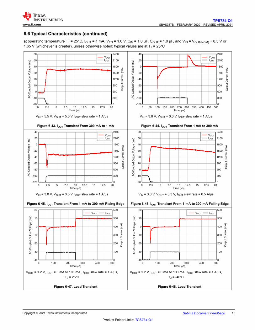
Figure 6-44. IOUT Transient From 1 mA to 300 mA
Time (Ps)
AC
-Coup
led O
utp
ut V
olta
ge (
mV
)
Ou
tpu
t C
urr
ent (m
A)
0 2.5 5 7.5 10 12.5 15 17.5 20-120 0
-100 300
-80 600
-60 900
-40 1200
-20 1500
0 1800
20 2100
40 2400VOUT
IOUT
VIN = 3.8 V, VOUT = 3.3 V, IOUT slew rate = 1 A/µs
Figure 6-45. IOUT Transient From 1-mA to 300-mA Rising Edge
Time (Ps)
AC
-Coup
led O
utp
ut V
olta
ge (
mV
)
Ou
tpu
t C
urr
ent (m
A)
0 2.5 5 7.5 10 12.5 15 17.5 20-20 0
-10 300
0 600
10 900
20 1200
30 1500
40 1800
50 2100
60 2400VOUT
IOUT
VIN = 3.8 V, VOUT = 3.3 V, IOUT slew rate = 0.5 A/µs
Figure 6-46. IOUT Transient From 1-mA to 300-mA Falling Edge
Time (Ps)
AC
-Coup
led O
utp
ut V
olta
ge (
mV
)
Ou
tpu
t C
urr
ent (m
A)
0 100 200 300 400 500-40 0
-30 100
-20 200
-10 300
0 400
10 500
20 600VOUT IOUT
VOUT = 1.2 V, IOUT = 0 mA to 100 mA , IOUT slew rate = 1 A/µs,TJ = 25℃
Figure 6-47. Load Transient
Time (Ps)
AC
-Coup
led O
utp
ut V
olta
ge (
mV
)
Ou
tpu
t C
urr
ent (m
A)
0 100 200 300 400 500-40 0
-30 100
-20 200
-10 300
0 400
10 500
20 600VOUT IOUT
VOUT = 1.2 V, IOUT = 0 mA to 100 mA , IOUT slew rate = 1 A/µs,TJ = -40℃
Figure 6-48. Load Transient
www.ti.comTPS784-Q1
SBVS387B – FEBRUARY 2020 – REVISED APRIL 2021
Copyright © 2021 Texas Instruments Incorporated Submit Document Feedback 15
Product Folder Links: TPS784-Q1

6.6 Typical Characteristics (continued)at operating temperature TJ = 25°C, IOUT = 1 mA, VEN = 1.0 V, CIN = 1.0 µF, COUT = 1.0 μF, and VIN = VOUT(NOM) + 0.5 V or1.65 V (whichever is greater), unless otherwise noted; typical values are at TJ = 25°C
Time (Ps)
AC
-Coup
led O
utp
ut V
olta
ge (
mV
)
Ou
tpu
t C
urr
ent (m
A)
0 100 200 300 400 500-40 0
-30 100
-20 200
-10 300
0 400
10 500
20 600VOUT IOUT
VOUT = 1.2 V, IOUT = 0 mA to 100 mA , IOUT slew rate = 1 A/µs,TJ = 150℃
Figure 6-49. Load Transient
Time (Ps)
AC
-Coup
led O
utp
ut V
olta
ge (
mV
)
Ou
tpu
t C
urr
ent (m
A)
0 100 200 300 400 500-60 0
-40 600
-20 1200
0 1800
20 2400
40 3000VOUT IOUT
VOUT = 1.2 V, IOUT = 0 mA to 300 mA , IOUT slew rate = 1 A/µs,TJ = 25℃
Figure 6-50. Load Transient
Time (Ps)
AC
-Coup
led O
utp
ut V
olta
ge (
mV
)
Ou
tpu
t C
urr
ent (m
A)
0 100 200 300 400 500-60 0
-40 600
-20 1200
0 1800
20 2400
40 3000VOUT IOUT
VOUT = 1.2 V, IOUT = 0 mA to 300 mA , IOUT slew rate = 1 A/µs,TJ = -40℃
Figure 6-51. Load Transient
Time (Ps)
AC
-Coup
led O
utp
ut V
olta
ge (
mV
)
Ou
tpu
t C
urr
ent (m
A)
0 100 200 300 400 500-100 0
-60 600
-20 1200
20 1800
60 2400VOUT IOUT
VOUT = 1.2 V, IOUT = 0 mA to 300 mA , IOUT slew rate = 1 A/µs,TJ = 150℃
Figure 6-52. Load Transient
Time (Ps)
AC
-Coup
led O
utp
ut V
olta
ge (
mV
)
Ou
tpu
t C
urr
ent (m
A)
0 40 80 120 160 200-20 0
-15 100
-10 200
-5 300
0 400
5 500
10 600VOUT
IOUT
VOUT = 1.2 V, IOUT = 90 mA to 200 mA,IOUT slew rate = 1 A/µs, TJ = 25℃
Figure 6-53. Load Transient
Time (Ps)
AC
-Coup
led O
utp
ut V
olta
ge (
mV
)
Ou
tpu
t C
urr
ent (m
A)
0 40 80 120 160 200-20 0
-15 100
-10 200
-5 300
0 400
5 500
10 600VOUT
IOUT
VOUT = 1.2 V, IOUT = 90 mA to 200 mA,IOUT slew rate = 1 A/µs, TJ = -40℃
Figure 6-54. Load Transient
TPS784-Q1SBVS387B – FEBRUARY 2020 – REVISED APRIL 2021 www.ti.com
16 Submit Document Feedback Copyright © 2021 Texas Instruments Incorporated
Product Folder Links: TPS784-Q1

6.6 Typical Characteristics (continued)at operating temperature TJ = 25°C, IOUT = 1 mA, VEN = 1.0 V, CIN = 1.0 µF, COUT = 1.0 μF, and VIN = VOUT(NOM) + 0.5 V or1.65 V (whichever is greater), unless otherwise noted; typical values are at TJ = 25°C
Time (Ps)
AC
-Coup
led O
utp
ut V
olta
ge (
mV
)
Ou
tpu
t C
urr
ent (m
A)
0 40 80 120 160 200-20 0
-15 100
-10 200
-5 300
0 400
5 500
10 600VOUT IOUT
VOUT = 1.2 V, IOUT = 90 mA to 200 mA,IOUT slew rate = 1 A/µs, TJ = 150℃
Figure 6-55. Load Transient
Time (Ps)
AC
-Coup
led O
utp
ut V
olta
ge (
mV
)
Ou
tpu
t C
urr
ent (m
A)
0 100 200 300 400 500-50 0
-40 100
-30 200
-20 300
-10 400
0 500
10 600
20 700
30 800VOUT IOUT
VOUT = 3.3 V, IOUT = 0 mA to 100 mA,IOUT slew rate = 1 A/µs, TJ = 25℃
Figure 6-56. Load Transient
Time (Ps)
AC
-Coup
led O
utp
ut V
olta
ge (
mV
)
Ou
tpu
t C
urr
ent (m
A)
0 100 200 300 400 500-50 0
-40 100
-30 200
-20 300
-10 400
0 500
10 600
20 700
30 800VOUT IOUT
VOUT = 3.3 V, IOUT = 0 mA to 100 mA, IOUT slew rate = 1 A/µs,TJ = -40℃
Figure 6-57. Load Transient
Time (Ps)
AC
-Coup
led O
utp
ut V
olta
ge (
mV
)
Ou
tpu
t cu
rren
t (m
A)
0 100 200 300 400 500-70 0
-60 100
-50 200
-40 300
-30 400
-20 500
-10 600
0 700
10 800
20 900
30 1000VOUT IOUT
VOUT = 3.3 V, IOUT = 0 mA to 100 mA, IOUT slew rate = 1 A/µs,TJ = 150℃
Figure 6-58. Load Transient
Time (Ps)
AC
-Coup
led O
utp
ut V
olta
ge (
mV
)
Ou
tpu
t C
urr
ent (m
A)
0 100 200 300 400 500-90 0
-70 200
-50 400
-30 600
-10 800
10 1000
30 1200
50 1400VOUT IOUT
VOUT = 3.3 V, IOUT = 0 mA to 300 mA, IOUT slew rate = 1 A/µs,TJ = 25℃
Figure 6-59. Load Transient
Time (Ps)
AC
-Coup
led O
utp
ut V
olta
ge (
mV
)
Ou
tpu
t C
urr
ent (m
A)
0 100 200 300 400 500-90 0
-70 200
-50 400
-30 600
-10 800
10 1000
30 1200
50 1400VOUT IOUT
VOUT = 3.3 V, IOUT = 0 mA to 300 mA, IOUT slew rate = 1 A/µs,TJ = -40℃
Figure 6-60. Load Transient
www.ti.comTPS784-Q1
SBVS387B – FEBRUARY 2020 – REVISED APRIL 2021
Copyright © 2021 Texas Instruments Incorporated Submit Document Feedback 17
Product Folder Links: TPS784-Q1

6.6 Typical Characteristics (continued)at operating temperature TJ = 25°C, IOUT = 1 mA, VEN = 1.0 V, CIN = 1.0 µF, COUT = 1.0 μF, and VIN = VOUT(NOM) + 0.5 V or1.65 V (whichever is greater), unless otherwise noted; typical values are at TJ = 25°C
Time (Ps)
AC
-Coup
led O
utp
ut V
olta
ge (
mV
)
Ou
tpu
t C
urr
ent (m
A)
0 100 200 300 400 500-110 0
-90 200
-70 400
-50 600
-30 800
-10 1000
10 1200
30 1400
50 1600VOUT IOUT
VOUT = 3.3 V, IOUT = 0 mA to 300 mA, IOUT slew rate = 1 A/µs,TJ = 150℃
Figure 6-61. Load Transient
Time (Ps)
AC
-Coup
led O
utp
ut V
olta
ge (
mV
)
Ou
tpu
t C
urr
ent (m
A)
0 100 200 300 400 500-25 0
-20 100
-15 200
-10 300
-5 400
0 500
5 600
10 700
15 800VOUT IOUT
VOUT = 3.3 V, IOUT = 90 mA to 200 mA,IOUT slew rate = 1 A/µs, TJ = 25℃
Figure 6-62. Load Transient
Time (Ps)
AC
-Coup
led O
utp
ut V
olta
ge (
mV
)
Ou
tpu
t C
urr
ent (m
A)
0 100 200 300 400 500-25 0
-20 100
-15 200
-10 300
-5 400
0 500
5 600
10 700
15 800VOUT IOUT
VOUT = 3.3 V, IOUT = 90 mA to 200 mA,IOUT slew rate = 1 A/µs, TJ = -40℃
Figure 6-63. Load Transient
Time (Ps)
AC
-Coup
led O
utp
ut V
olta
ge (
mV
)
Ou
tpu
t C
urr
ent (m
A)
0 100 200 300 400 500-25 0
-20 100
-15 200
-10 300
-5 400
0 500
5 600
10 700
15 800VOUT IOUT
VOUT = 3.3 V, IOUT = 90 mA to 200 mA,IOUT slew rate = 1 A/µs, TJ = 150℃
Figure 6-64. Load Transient
Frequency (Hz)
Pow
er
Sup
ply
Reje
ctio
n R
atio (
dB
)
0
10
20
30
40
50
60
70
80
90
10 100 1k 10k 100k 1M 10M
IOUT
1 mA10 mA
50 mA100 mA
200 mA300 mA
VIN = 1.65 V, CIN = 0 µF, VOUT = 0.65 V
Figure 6-65. PSRR vs Frequency and IOUT
Frequency (Hz)
Pow
er
Sup
ply
Reje
jctio
n R
atio (
dB
)
0
10
20
30
40
50
60
70
80
90
10 100 1k 10k 100k 1M 10M
IOUT
1 mA10 mA50 mA
100 mA200 mA300 mA
VIN = 2.2 V, CIN = 0 µF, VOUT = 1.2 V
Figure 6-66. PSRR vs Frequency and IOUT
TPS784-Q1SBVS387B – FEBRUARY 2020 – REVISED APRIL 2021 www.ti.com
18 Submit Document Feedback Copyright © 2021 Texas Instruments Incorporated
Product Folder Links: TPS784-Q1

6.6 Typical Characteristics (continued)at operating temperature TJ = 25°C, IOUT = 1 mA, VEN = 1.0 V, CIN = 1.0 µF, COUT = 1.0 μF, and VIN = VOUT(NOM) + 0.5 V or1.65 V (whichever is greater), unless otherwise noted; typical values are at TJ = 25°C
Frequency (Hz)
Pow
er
Sup
ply
Reje
ctio
n R
atio (
dB
)
0
10
20
30
40
50
60
70
80
90
10 100 1k 10k 100k 1M 10M
IOUT
1 mA10 mA
50 mA100 mA
200 mA300 mA
VIN = 4.3 V, CIN = 0 µF, VOUT = 3.3 V
Figure 6-67. PSRR vs Frequency and IOUT
Frequency (Hz)
Pow
er
Sup
ply
Reje
ctio
n R
atio (
dB
)
0
10
20
30
40
50
60
70
80
90
10 100 1k 10k 100k 1M 10M
COUT
1.0 PF 4.7 PF 10 PF
VIN = 4.3 V, CIN = 0 µF, VOUT = 3.3 V, IOUT = 300 mA
Figure 6-68. PSRR vs Frequency and COUT
Frequency (Hz)
Pow
er
Supply
Reje
ction R
atio
(dB
)
0
10
20
30
40
50
60
70
80
90
100
110
10 100 1k 10k 100k 1M 10M
VDO (mV)200 mV300 mV
400 mV500 mV
600 mV700 mV
1 V
CIN = 0 µF, VOUT = 3.3 V, IOUT = 300 mA
Figure 6-69. PSRR vs Frequency and VDO
Frequency (Hz)
Pow
er
Sup
ply
Reje
ctio
n R
atio (
dB
)
0
10
20
30
40
50
60
70
80
90
10 100 1k 10k 100k 1M 10M
IOUT
1 mA10 mA
50 mA100 mA
200 mA300 mA
VIN = 6 V, CIN = 0 µF, VOUT = 5.0 V
Figure 6-70. PSRR vs Frequency and IOUT
Frequency (Hz)
Pow
er
Supply
Reje
ction R
atio (
dB
)
0
10
20
30
40
50
60
70
80
90
10 100 1k 10k 100k 1M 10M
COUT
1.0 µF 4.7 µF 10 µF
VIN = 6 V, CIN = 0 µF, VOUT = 5.0 V, IOUT = 300 mA
Figure 6-71. PSRR vs Frequency and COUT
Frequency (Hz)
Outp
ut V
olta
ge N
ois
e (PV
/�H
z)
0.005
0.01
0.020.03
0.05
0.1
0.20.3
0.5
1
23
55
10 100 1k 10k 100k 1M 10M
(VOUT), (PVRMS)(1.2 V), (29.6)(0.65V), (40.6)(3.3 V), (75.8)(5.0 V), (110.4)
VIN = VOUT(nom) + 1 V, IOUT = 300 mA,VRMS BW = 10 Hz to 100 kHz
Figure 6-72. Output Noise vs Frequency and VOUT
www.ti.comTPS784-Q1
SBVS387B – FEBRUARY 2020 – REVISED APRIL 2021
Copyright © 2021 Texas Instruments Incorporated Submit Document Feedback 19
Product Folder Links: TPS784-Q1

6.6 Typical Characteristics (continued)at operating temperature TJ = 25°C, IOUT = 1 mA, VEN = 1.0 V, CIN = 1.0 µF, COUT = 1.0 μF, and VIN = VOUT(NOM) + 0.5 V or1.65 V (whichever is greater), unless otherwise noted; typical values are at TJ = 25°C
Frequency (Hz)
Outp
ut V
olta
ge N
ois
e (PV
/�H
z)
0.005
0.01
0.020.03
0.05
0.1
0.20.3
0.5
1
23
55
10 100 1k 10k 100k 1M 10M
(CFF (nF)), (PVRMS)(Open), (75.8)(1), (62.3)(4.7), (54.7)(10), (49.7)(100), (37.6)
VIN = 4.3 V, VOUT = 3.3 V, IOUT = 300 mA,VRMS BW = 10 Hz to 100 kHz
Figure 6-73. Output Noise vs Frequency and CFF
Frequency (Hz)
Outp
ut V
olta
ge N
ois
e (PV
/�H
z)
0.005
0.01
0.02
0.05
0.1
0.2
0.5
1
2
5
10
10 100 1k 10k 100k 1M 10M
(CFF (nF)), (PVRMS)(Open), (110.4)(1), (91.1)(4.7), (79.2)(10), (70.7)(100), (42.1)
VIN = 6 V, VOUT = 5.0 V, IOUT = 300 mA,VRMS BW = 10 Hz to 100 kHz
Figure 6-74. Output Noise vs Frequency and CFF
Time (ms)
Voltag
e (
V)
Inp
ut C
urr
en
t (m
A)
0 0.1 0.2 0.3 0.4 0.5 0.6 0.7 0.8 0.9 1-1 -140
0 -120
1 -100
2 -80
3 -60
4 -40
5 -20
6 0
7 20
8 40
VIN
VEN
VOUT
IIN
VIN = 5.5 V, CIN = 0 µF, COUT = 1 µF, VOUT = 5.0 V,IOUT = 0 mA
Figure 6-75. Start-Up Inrush Current WithCOUT = 1 µF
Time (ms)
Voltag
e (
V)
Inp
ut C
urr
en
t (m
A)
0 0.1 0.2 0.3 0.4 0.5 0.6 0.7 0.8 0.9 1-1 -140
0 -120
1 -100
2 -80
3 -60
4 -40
5 -20
6 0
7 20
8 40
VIN
VEN
VOUT
IIN
VIN = VEN = 5.5 V, CIN = 0 µF, COUT = 1 µF, VOUT = 5.0 V,IOUT = 0 mA
Figure 6-76. Start-Up Inrush Current WithCOUT = 1 µF
Time (ms)
Vo
lta
ge
(V
)
Inp
ut C
urr
en
t (m
A)
0 0.1 0.2 0.3 0.4 0.5 0.6 0.7 0.8 0.9 1-1 -560
0 -480
1 -400
2 -320
3 -240
4 -160
5 -80
6 0
7 80
8 160
VIN
VEN
VOUT
IIN
VIN = 5.5 V, CIN = 0 µF, COUT = 4.7 µF, VOUT = 5.0 V,IOUT = 0 mA
Figure 6-77. Start-Up Inrush Current WithCOUT = 4.7 µF
Time (Ps)
Vo
ltag
e (
V)
Ou
tpu
t C
urr
en
t (m
A)
0 200 400 600 800 1000 1200 1400 1600 1800 2000-1 -40
0 0
1 40
2 80
3 120
4 160
5 200
6 240
7 280Input VoltageEnable Voltage
Output VoltageOutput Current
VIN = 5 V, CIN = 1 µF, COUT = 10 µF, VOUT = 1.2 V,IOUT = 500 mA
Figure 6-78. Start Up at –40°C
TPS784-Q1SBVS387B – FEBRUARY 2020 – REVISED APRIL 2021 www.ti.com
20 Submit Document Feedback Copyright © 2021 Texas Instruments Incorporated
Product Folder Links: TPS784-Q1

6.6 Typical Characteristics (continued)at operating temperature TJ = 25°C, IOUT = 1 mA, VEN = 1.0 V, CIN = 1.0 µF, COUT = 1.0 μF, and VIN = VOUT(NOM) + 0.5 V or1.65 V (whichever is greater), unless otherwise noted; typical values are at TJ = 25°C
Time (Ps)
Vo
ltag
e (
V)
Ou
tpu
t C
urr
en
t (m
A)
0 200 400 600 800 1000 1200 1400 1600 1800 2000-1 -40
0 0
1 40
2 80
3 120
4 160
5 200
6 240
7 280Input VoltageEnable Voltage
Output VoltageOutput Current
VIN = 5 V, CIN = 1 µF, COUT = 10 µF, VOUT = 1.2 V,IOUT = 500 mA
Figure 6-79. Start Up at 25°C
Time (Ps)
Vo
ltag
e (
V)
Ou
tpu
t C
urr
en
t (m
A)
0 200 400 600 800 1000 1200 1400 1600 1800 2000-1 -40
0 0
1 40
2 80
3 120
4 160
5 200
6 240
7 280Input VoltageEnable Voltage
Output VoltageOutput Current
VIN = 5 V, CIN = 1 µF, COUT = 10 µF, VOUT = 1.2 V,IOUT = 500 mA
Figure 6-80. Start Up at 150°C
Temperature (qC)-50 -25 0 25 50 75 100 125 150 175 200
ON
OFF
VIN = 5 V, CIN = 1 µF, COUT = 10 µF, VOUT = 1.2 V,IOUT = 500 mA
Figure 6-81. Thermal Shutdown Activation
COUT (PF)
ES
R (:
)
0.5 1 2 3 4 5 67 10 20 30 50 70100 200 5000.0005
0.001
0.002
0.005
0.01
0.02
0.05
0.1
0.2
0.5
1
2
55
xxxxxxxxxxxxxxxxxxxxxxxxxxxxxxxxxxxxxx
xxxxxxxxx
xxxxxxxxx
xxxxxxxxx
xxxxxxxxxxxx
xxxxxxxxxxxx
xxxxxxxxxxxxxxxx
xxxxxxxxxxxxxxxx
xxxxxxxxxxxxxxxx
xxxxxxxxxxxx
xxxxxxxxxxxxxxxx
xxxxxxxxxxxxxxxx
xxxxxxxxxxxxxxxx
xxxxxxxxxxxxxxxx
xxxxxxxxxxxxxxxx
xxxxxxxxxxxx
xxxxxxxxxxxx
xxxxxxxxxxxxxxxx
xxxxxxxxxxxxxxxx
xxxxxxxxxxxxxxxx
xxxxxxxxxxxxxxxx
xxxxxxxxxxxx
xxxxxxxxxxxx
xxxxxxxxxxxx
xxxxxxxxxxxx
xxxxxxxxx
xxxxxxxxx
xxxxxxxxx
xxxxxx
xxxxxx
xxxxxxxxxxxxxxxx
xxxx
Stable region
COUT denotes nominal capacitor size(not effective capacitance)
Figure 6-82. ESR vs COUT
www.ti.comTPS784-Q1
SBVS387B – FEBRUARY 2020 – REVISED APRIL 2021
Copyright © 2021 Texas Instruments Incorporated Submit Document Feedback 21
Product Folder Links: TPS784-Q1

7 Detailed Description7.1 OverviewThe TPS784-Q1 is an ultra low-dropout, high PSRR, high-accuracy linear voltage regulator that is optimized forexcellent transient performance. These characteristics make the device ideal for most automotive applications.
This regulator offers foldback current limit, output enable, active discharge, undervoltage lockout (UVLO), andthermal protection.
7.2 Functional Block Diagrams
+±
1.2-V
Bandgap
Thermal
Shutdown
UVLO
Internal
Controller
Current
Limit
120 ��
IN
EN
GND
OUT
FB
Figure 7-1. Adjustable Version Block Diagram
+±
1.2-V
Bandgap
Thermal
Shutdown
UVLO
Internal
Controller
Current
Limit
120 ��
IN
EN
GND
OUT
550 k
2.42 M
2.18 M
Figure 7-2. Fixed Version Block Diagram
TPS784-Q1SBVS387B – FEBRUARY 2020 – REVISED APRIL 2021 www.ti.com
22 Submit Document Feedback Copyright © 2021 Texas Instruments Incorporated
Product Folder Links: TPS784-Q1

7.3 Feature Description7.3.1 Foldback Current Limit
The device has an internal current limit circuit that protects the regulator during transient high-load current faultsor shorting events. The current limit is a hybrid brickwall-foldback scheme. The current limit transitions from abrickwall scheme to a foldback scheme at the foldback voltage (VFOLDBACK). In a high-load current fault withthe output voltage above VFOLDBACK, the brickwall scheme limits the output current to the current limit (ICL).When the voltage drops below VFOLDBACK, a foldback current limit activates that scales back the current as theoutput voltage approaches GND. When the output is shorted, the device supplies a typical current called theshort-circuit current limit (ISC). ICL and ISC are listed in the Electrical Characteristics table.
For this device, VFOLDBACK = 0.4 × VOUT(NOM).
The output voltage is not regulated when the device is in current limit. When a current limit event occurs, thedevice begins to heat up because of the increase in power dissipation. When the device is in brickwall currentlimit, the pass transistor dissipates power [(VIN – VOUT) × ICL]. When the device output is shorted and the outputis below VFOLDBACK, the pass transistor dissipates power [(VIN – VOUT) × ISC]. If thermal shutdown is triggered,the device turns off. After the device cools down, the internal thermal shutdown circuit turns the device back on.If the output current fault condition continues, the device cycles between current limit and thermal shutdown. Formore information on current limits, see the Know Your Limits application report.
Figure 7-3 shows a diagram of the foldback current limit.
VOUT(NOM)
0 V
0 mA
VOUT
VFOLDBACK
ICLISC IRATED
IOUT
Brickwall
Foldback
Figure 7-3. Foldback Current Limit
7.3.2 Output Enable
The enable pin (EN) is active high. Enable the device by forcing the voltage of the enable pin to exceed theminimum EN pin high-level input voltage (see the Electrical Characteristics table). Turn off the device by forcingthe voltage of the enable pin to drop below the maximum EN pin low-level input voltage (see the ElectricalCharacteristics table). If shutdown capability is not required, connect EN to IN.
This device has an internal pulldown circuit that activates when the device is disabled to actively discharge theoutput voltage.
www.ti.comTPS784-Q1
SBVS387B – FEBRUARY 2020 – REVISED APRIL 2021
Copyright © 2021 Texas Instruments Incorporated Submit Document Feedback 23
Product Folder Links: TPS784-Q1

7.3.3 Active Discharge
The device has an internal pulldown MOSFET that connects an RPULLDOWN resistor to ground when the device isdisabled to actively discharge the output voltage. The active discharge circuit is activated by the enable pin.
Do not rely on the active discharge circuit to discharge the output voltage after the input supply has collapsedbecause reverse current can possibly flow from the output to the input. This reverse current flow can causedamage to the device, especially when a large output capacitor is used. Limit reverse current to no more than5% of the device rated current for a short period of time.
7.3.4 Undervoltage Lockout (UVLO) Operation
The UVLO circuit ensures that the device stays disabled before its input supply reaches the minimumoperational voltage range, and ensures that the device shuts down when the input supply collapses. Figure7-4 shows the UVLO circuit response to various input voltage events. The diagram can be separated into thefollowing parts:
• Region A: The device does not start until the input reaches the UVLO rising threshold.• Region B: Normal operation, regulating device.• Region C: Brownout event above the UVLO falling threshold (UVLO rising threshold – UVLO hysteresis). The
output may fall out of regulation but the device remains enabled.• Region D: Normal operation, regulating device.• Region E: Brownout event below the UVLO falling threshold. The device is disabled in most cases and the
output falls because of the load and active discharge circuit. The device is reenabled when the UVLO risingthreshold is reached by the input voltage and a normal start-up follows.
• Region F: Normal operation followed by the input falling to the UVLO falling threshold.• Region G: The device is disabled when the input voltage falls below the UVLO falling threshold to 0 V. The
output falls because of the load and active discharge circuit.
C
tAt
VIN
VOUT
UVLO Rising Threshold
UVLO Hysteresis
tBt tDt tEt tFt tGt
Figure 7-4. Typical UVLO Operation
7.3.5 Dropout Voltage
Dropout voltage (VDO) is defined as the input voltage minus the output voltage (VIN – VOUT) at the rated outputcurrent (IRATED), where the pass transistor is fully on. IRATED is the maximum IOUT listed in the RecommendedOperating Conditions table. The pass transistor is in the ohmic or triode region of operation, and acts as aswitch. The dropout voltage indirectly specifies a minimum input voltage greater than the nominal programmedoutput voltage at which the output voltage is expected to stay in regulation. If the input voltage falls to less thanthe nominal output regulation, then the output voltage falls as well.
For a CMOS regulator, the dropout voltage is determined by the drain-source on-state resistance (RDS(ON)) of thepass transistor. Therefore, if the linear regulator operates at less than the rated current, the dropout voltage forthat current scales accordingly. The following equation calculates the RDS(ON) of the device.
R =DS(ON)
VDO
IRATED (1)
TPS784-Q1SBVS387B – FEBRUARY 2020 – REVISED APRIL 2021 www.ti.com
24 Submit Document Feedback Copyright © 2021 Texas Instruments Incorporated
Product Folder Links: TPS784-Q1

7.3.6 Thermal Shutdown
The device contains a thermal shutdown protection circuit to disable the device when the junction temperature(TJ) of the pass transistor rises to TSD(shutdown) (typical). Thermal shutdown hysteresis assures that the deviceresets (turns on) when the temperature falls to TSD(reset) (typical).
The thermal time-constant of the semiconductor die is fairly short, thus the device may cycle on and offwhen thermal shutdown is reached until power dissipation is reduced. Power dissipation during startup canbe high from large VIN – VOUT voltage drops across the device or from high inrush currents charging largeoutput capacitors. Under some conditions, the thermal shutdown protection disables the device before startupcompletes.
For reliable operation, limit the junction temperature to the maximum listed in the Recommended OperatingConditions table. Operation above this maximum temperature causes the device to exceed its operationalspecifications. Although the internal protection circuitry of the device is designed to protect against thermaloverall conditions, this circuitry is not intended to replace proper heat sinking. Continuously running the deviceinto thermal shutdown or above the maximum recommended junction temperature reduces long-term reliability.
www.ti.comTPS784-Q1
SBVS387B – FEBRUARY 2020 – REVISED APRIL 2021
Copyright © 2021 Texas Instruments Incorporated Submit Document Feedback 25
Product Folder Links: TPS784-Q1

7.4 Device Functional Modes7.4.1 Device Functional Mode Comparison
The Device Functional Mode Comparison table shows the conditions that lead to the different modes ofoperation. See the Electrical Characteristics table for parameter values.
Table 7-1. Device Functional Mode Comparison
OPERATING MODEPARAMETER
VIN VEN IOUT TJ
Normal operation VIN > VOUT(nom) + VDO and VIN > VIN(min) VEN > VEN(HI) IOUT < IOUT(max) TJ < TSD(shutdown)
Dropout operation VIN(min) < VIN < VOUT(nom) + VDO VEN > VEN(HI) IOUT < IOUT(max) TJ < TSD(shutdown)
Disabled(any true conditiondisables the device)
VIN < VUVLO VEN < VEN(LOW) Not applicable TJ > TSD(shutdown)
7.4.2 Normal Operation
The device regulates to the nominal output voltage when the following conditions are met:
• The input voltage is greater than the nominal output voltage plus the dropout voltage (VOUT(nom) + VDO)• The output current is less than the current limit (IOUT < ICL)• The device junction temperature is less than the thermal shutdown temperature (TJ < TSD)
• The enable voltage has previously exceeded the enable rising threshold voltage and has not yet decreasedto less than the enable falling threshold
7.4.3 Dropout Operation
If the input voltage is lower than the nominal output voltage plus the specified dropout voltage, but all otherconditions are met for normal operation, the device operates in dropout mode. In this mode, the output voltagetracks the input voltage. During this mode, the transient performance of the device becomes significantlydegraded because the pass transistor is in the ohmic or triode region, and acts as a switch. Line or loadtransients in dropout can result in large output-voltage deviations.
When the device is in a steady dropout state (defined as when the device is in dropout, VIN < VOUT(NOM) + VDO,directly after being in a normal regulation state, but not during startup), the pass transistor is driven into theohmic or triode region. When the input voltage returns to a value greater than or equal to the nominal outputvoltage plus the dropout voltage (VOUT(NOM) + VDO), the output voltage can overshoot for a short period of timewhile the device pulls the pass transistor back into the linear region.
7.4.4 Disabled
The output of the device can be shutdown by forcing the voltage of the enable pin to less than the maximumEN pin low-level input voltage (see the Electrical Characteristics table). When disabled, the pass transistor isturned off, internal circuits are shutdown, and the output voltage is actively discharged to ground by an internaldischarge circuit from the output to ground.
TPS784-Q1SBVS387B – FEBRUARY 2020 – REVISED APRIL 2021 www.ti.com
26 Submit Document Feedback Copyright © 2021 Texas Instruments Incorporated
Product Folder Links: TPS784-Q1

8 Application and ImplementationNote
Information in the following applications sections is not part of the TI component specification,and TI does not warrant its accuracy or completeness. TI’s customers are responsible fordetermining suitability of components for their purposes, as well as validating and testing their designimplementation to confirm system functionality.
8.1 Application Information8.1.1 Recommended Capacitor Types
The device is designed to be stable using low equivalent series resistance (ESR) ceramic capacitors at the inputand output. Multilayer ceramic capacitors have become the industry standard for these types of applications andare recommended, but must be used with good judgment. Ceramic capacitors that employ X7R-, X5R-, andC0G-rated dielectric materials provide relatively good capacitive stability across temperature, whereas the use ofY5V-rated capacitors is discouraged because of large variations in capacitance.
Regardless of the ceramic capacitor type selected, the effective capacitance varies with operating voltage andtemperature. As a rule of thumb, expect the effective capacitance to decrease by as much as 50%. The inputand output capacitors recommended in the Recommended Operating Conditions table account for an effectivecapacitance of approximately 50% of the nominal value.
8.1.2 Input and Output Capacitor Requirements
The device requires an input capacitor of 1.0 µF or larger as specified in the Recommended OperatingConditions table for stability. A higher value capacitor may be necessary if large, fast rise-time load or linetransients are anticipated or if the device is located several inches from the input power source.
The device also requires an output capacitor of 1.0 µF or larger as specified in the Recommended OperatingConditions table for stability. Dynamic performance of the device is improved by using a higher capacitor thanthe minimum output capacitor.
8.1.3 Adjustable Device Feedback Resistors
The device requires external feedback divider resistors to set the output voltage. Figure 8-1 shows how theoutput voltage of an adjustable device can be configured from 1.2 V to 5.5 V by using a resistor divider network.
TPS784-Q1
IN
EN
OUT
GND
COUTCIN CFFR1
R2
Feed-Forward capacitor CFF is not required for stability (Optional)
FB
GND
GND
VIN
VEN
VOUT
Figure 8-1. Adjustable Operation
Equation 2 calculates the values of the R1 and R2 resistors to set the output voltage:
VOUT = VFB × (1 + R1 / R2) + IFB × R1 (2)
www.ti.comTPS784-Q1
SBVS387B – FEBRUARY 2020 – REVISED APRIL 2021
Copyright © 2021 Texas Instruments Incorporated Submit Document Feedback 27
Product Folder Links: TPS784-Q1

To disregard the effect of the FB pin current error term in Equation 2 and to achieve best accuracy, chooseR2 to be equal to or smaller than 550 kΩ so that the current flowing through R1 and R2 is at least 100 timeslarger than the IFB current listed in the Electrical Characteristics table. Lowering the value of R2 increases theimmunity against noise injection. Increasing the value of R2 reduces the quiescent current for achieving higherefficiency at low load currents. Equation 3 calculates the setting that provides the maximum feedback dividerseries resistance.
(R1 + R2) ≤ VOUT / (IFB × 100) (3)
8.1.4 Load Transient Response
The load-step transient response is the output voltage response by the LDO to a step in load current, wherebyoutput voltage regulation is maintained. There are two key transitions during a load transient response: thetransition from a light to a heavy load and the transition from a heavy to a light load. The regions shown in Figure8-2 are broken down as follows. Regions A, E, and H are where the output voltage is in steady-state.
tAt tDt tEttCt tGt tHt
FB
Figure 8-2. Load Transient Waveform
During transitions from a light load to a heavy load, the:
• Initial voltage dip is a result of the depletion of the output capacitor charge and parasitic impedance to theoutput capacitor (region B)
• Recovery from the dip results from the LDO increasing its sourcing current, and leads to output voltageregulation (region C)
• Initial voltage rise results from the LDO sourcing a large current, and leads to the output capacitor charge toincrease (region F)
• Recovery from the rise results from the LDO decreasing its sourcing current in combination with the loaddischarging the output capacitor (region G)
A larger output capacitance reduces the peaks during a load transient but slows down the response time of thedevice. A larger DC load also reduces the peaks because the amplitude of the transition is lowered and a highercurrent discharge path is provided for the output capacitor.
TPS784-Q1SBVS387B – FEBRUARY 2020 – REVISED APRIL 2021 www.ti.com
28 Submit Document Feedback Copyright © 2021 Texas Instruments Incorporated
Product Folder Links: TPS784-Q1
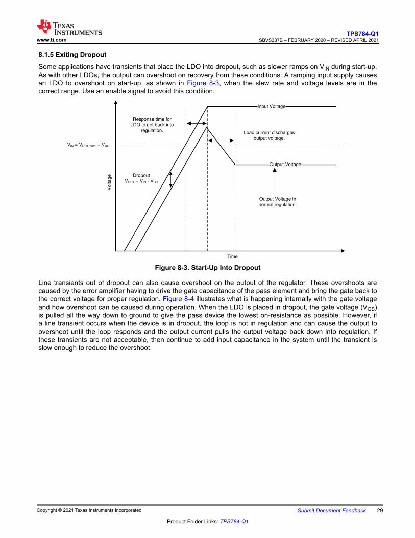
8.1.5 Exiting Dropout
Some applications have transients that place the LDO into dropout, such as slower ramps on VIN during start-up.As with other LDOs, the output can overshoot on recovery from these conditions. A ramping input supply causesan LDO to overshoot on start-up, as shown in Figure 8-3, when the slew rate and voltage levels are in thecorrect range. Use an enable signal to avoid this condition.
Input Voltage
Output Voltage
Output Voltage in
normal regulation.
Dropout
VOUT = VIN - VDO
VIN = VOUT(nom) + VDO
Response time for
LDO to get back into
regulation. Load current discharges
output voltage.
Vo
lta
ge
Time
Figure 8-3. Start-Up Into Dropout
Line transients out of dropout can also cause overshoot on the output of the regulator. These overshoots arecaused by the error amplifier having to drive the gate capacitance of the pass element and bring the gate back tothe correct voltage for proper regulation. Figure 8-4 illustrates what is happening internally with the gate voltageand how overshoot can be caused during operation. When the LDO is placed in dropout, the gate voltage (VGS)is pulled all the way down to ground to give the pass device the lowest on-resistance as possible. However, ifa line transient occurs when the device is in dropout, the loop is not in regulation and can cause the output toovershoot until the loop responds and the output current pulls the output voltage back down into regulation. Ifthese transients are not acceptable, then continue to add input capacitance in the system until the transient isslow enough to reduce the overshoot.
www.ti.comTPS784-Q1
SBVS387B – FEBRUARY 2020 – REVISED APRIL 2021
Copyright © 2021 Texas Instruments Incorporated Submit Document Feedback 29
Product Folder Links: TPS784-Q1

Output Voltage in
normal regulation
Dropout
VOUT = VIN - VDO
Transient response
time of the LDO
Load current
discharges
output
voltage
Vo
lta
ge
Time
VGS voltage for
normal operation
VGS voltage in
dropout (pass device
fully on)
VDO
Gate Voltage
Input Voltage
VGS voltage for
normal operation
Input Voltage
Output Voltage
VGS voltage
(pass device
fully off)
Time
Vo
lta
ge
Figure 8-4. Line Transients From Dropout
8.1.6 Dropout Voltage
The device uses a PMOS pass transistor to achieve low dropout. When (VIN – VOUT) is less than the dropoutvoltage (VDO), the PMOS pass device is in the linear region of operation and the input-to-output resistance is theRDS(ON) of the PMOS pass element. VDO scales approximately with output current because the PMOS devicebehaves like a resistor in dropout mode. As with any linear regulator, PSRR and transient response degrade as(VIN – VOUT) approaches dropout operation.
8.1.7 Reverse Current
As with most LDOs, excessive reverse current can damage this device.
Reverse current flows through the body diode on the pass element instead of the normal conducting channel.At high magnitudes, this current flow degrades the long-term reliability of the device as a result of one of thefollowing conditions:• Degradation caused by electromigration• Excessive heat dissipation• Potential for a latch-up condition
TPS784-Q1SBVS387B – FEBRUARY 2020 – REVISED APRIL 2021 www.ti.com
30 Submit Document Feedback Copyright © 2021 Texas Instruments Incorporated
Product Folder Links: TPS784-Q1

Conditions where reverse current can occur are outlined in this section, all of which can exceed the absolutemaximum rating of VOUT > VIN + 0.3 V:• If the device has a large COUT and the input supply collapses with little or no load current• The output is biased when the input supply is not established• The output is biased above the input supply
If reverse current flow is expected in the application, external protection must be used to protect the device.Figure 8-5 shows one approach of protecting the device.
Device
IN OUT
GND
COUT
CIN
Schottky Diode
Internal Body Diode
Figure 8-5. Example Circuit for Reverse Current Protection Using a Schottky Diode
8.1.8 Feed-Forward Capacitor (CFF)
For the adjustable-voltage version device, a feed-forward capacitor (CFF) can be connected from the OUT pinto the FB pin. CFF improves transient, noise, and PSRR performance, but is not required for regulator stability.Recommended CFF values are listed in the Recommended Operating Conditions table. A higher capacitanceCFF can be used; however, the startup time increases. For a detailed description of CFF tradeoffs, see the Prosand Cons of Using a Feedforward Capacitor with a Low-Dropout Regulator application report.
8.1.9 Power Dissipation (PD)
Circuit reliability demands that proper consideration be given to device power dissipation, location of the circuiton the printed circuit board (PCB), and correct sizing of the thermal plane. The PCB area around the regulatormust be as free as possible of other heat-generating devices that cause added thermal stresses.
As a first-order approximation, power dissipation in the regulator depends on the input-to-output voltagedifference and load conditions. Use Equation 4 to approximate PD:
PD = (VIN – VOUT) × IOUT (4)
Power dissipation can be minimized, and thus greater efficiency achieved, by proper selection of the systemvoltage rails. Proper selection allows the minimum input-to-output voltage differential to be obtained. The lowdropout of the TPS784-Q1 allows for maximum efficiency across a wide range of output voltages.
The main heat conduction path for the device is through the thermal pad on the package. As such, the thermalpad must be soldered to a copper pad area under the device. This pad area contains an array of plated vias thatconduct heat to any inner plane areas or to a bottom-side copper plane.
The maximum power dissipation determines the maximum allowable junction temperature (TJ) for the device.According to Equation 5, power dissipation and junction temperature are most often related by the junction-to-ambient thermal resistance (RθJA) of the combined PCB and device package and the temperature of the ambientair (TA). Equation 6 rearranges Equation 5 for output current.
TJ = TA + (RθJA × PD) (5)
IOUT = (TJ – TA) / [RθJA × (VIN – VOUT)] (6)
Unfortunately, this thermal resistance (RθJA) is highly dependent on the heat-spreading capability built into theparticular PCB design, and therefore varies according to the total copper area, copper weight, and location
www.ti.comTPS784-Q1
SBVS387B – FEBRUARY 2020 – REVISED APRIL 2021
Copyright © 2021 Texas Instruments Incorporated Submit Document Feedback 31
Product Folder Links: TPS784-Q1

of the planes. The RθJA recorded in the Recommended Operating Conditions table is determined by theJEDEC standard, PCB, and copper-spreading area, and is only used as a relative measure of package thermalperformance. For a well-designed thermal layout, RθJA is actually the sum of the VSON package junction-to-case(bottom) thermal resistance (RθJC(bot)) plus the thermal resistance contribution by the PCB copper.
8.1.9.1 Estimating Junction Temperature
The JEDEC standard now recommends the use of psi (Ψ) thermal metrics to estimate the junction temperaturesof the LDO when in-circuit on a typical PCB board application. These metrics are not strictly speaking thermalresistances, but rather offer practical and relative means of estimating junction temperatures. These psi metricsare determined to be significantly independent of the copper-spreading area. The key thermal metrics (ΨJT andΨJB) are used in accordance with Equation 7 and are given in the Recommended Operating Conditions table.
ΨJT : TJ = TT + ΨJT × PD and ΨJB : TJ = TB + ΨJB × PD (7)
where:
• PD is the power dissipated as explained in Equation 4• TT is the temperature at the center-top of the device package, and• TB is the PCB surface temperature measured 1 mm from the device package and centered on the package
edge
8.1.9.2 Recommended Area for Continuous Operation
The operational area of an LDO is limited by the dropout voltage, output current, junction temperature, and inputvoltage. The recommended area for continuous operation for a linear regulator is given in Figure 8-6 and can beseparated into the following parts:
• Dropout voltage limits the minimum differential voltage between the input and the output (VIN – VOUT) at agiven output current level. See the Dropout Voltage section for more details.
• The rated output currents limits the maximum recommended output current level. Exceeding this ratingcauses the device to fall out of specification.
• The rated junction temperature limits the maximum junction temperature of the device. Exceeding this ratingcauses the device to fall out of specification and reduces long-term reliability.– The shape of the slope is given by Equation 6. The slope is nonlinear because the maximum rated
junction temperature of the LDO is controlled by the power dissipation across the LDO; thus when VIN –VOUT increases the output current must decrease.
• The rated input voltage range governs both the minimum and maximum of VIN – VOUT.
TPS784-Q1SBVS387B – FEBRUARY 2020 – REVISED APRIL 2021 www.ti.com
32 Submit Document Feedback Copyright © 2021 Texas Instruments Incorporated
Product Folder Links: TPS784-Q1

Figure 8-6 shows the recommended area of operation for this device on a JEDEC-standard high-K board with aRθJA as given in the Recommended Operating Conditions table.
Rated output current
Output current limited by dropout
Output current limited by thermals
Limited by minimum VIN
Limited by maximum VIN
VIN ± VOUT (V)
Ou
tpu
t c
urr
en
t (A
)
Figure 8-6. Region Description of Continuous Operation Regime
8.1.9.3 Power Dissipation versus Ambient Temperature
Figure 8-7 is based off of a JESD51-7 four-layer high-K board. The allowable power dissipation was estimatedusing the following equation. As disscussed in the An empirical analysis of the impact of board layout onLDO thermal performance application report, thermal dissipation can be improved in the JEDEC high-K layoutby adding top layer copper and increasing the number of thermal vias. If a good thermal layout is used, theallowable thermal dissipation can be improved by up to 50%.
6# + 4à,# T 2& Q 150 °% (8)
Ambient Temerature (qC)
Ma
xim
um
Pow
er
Dis
sip
atio
n (
W)
-40 -20 0 20 40 60 80 100 120 1400
0.2
0.4
0.6
0.8
1
1.2
1.4
1.6DRB PackageDBV Package
Figure 8-7. Allowable Power Dissipation
www.ti.comTPS784-Q1
SBVS387B – FEBRUARY 2020 – REVISED APRIL 2021
Copyright © 2021 Texas Instruments Incorporated Submit Document Feedback 33
Product Folder Links: TPS784-Q1
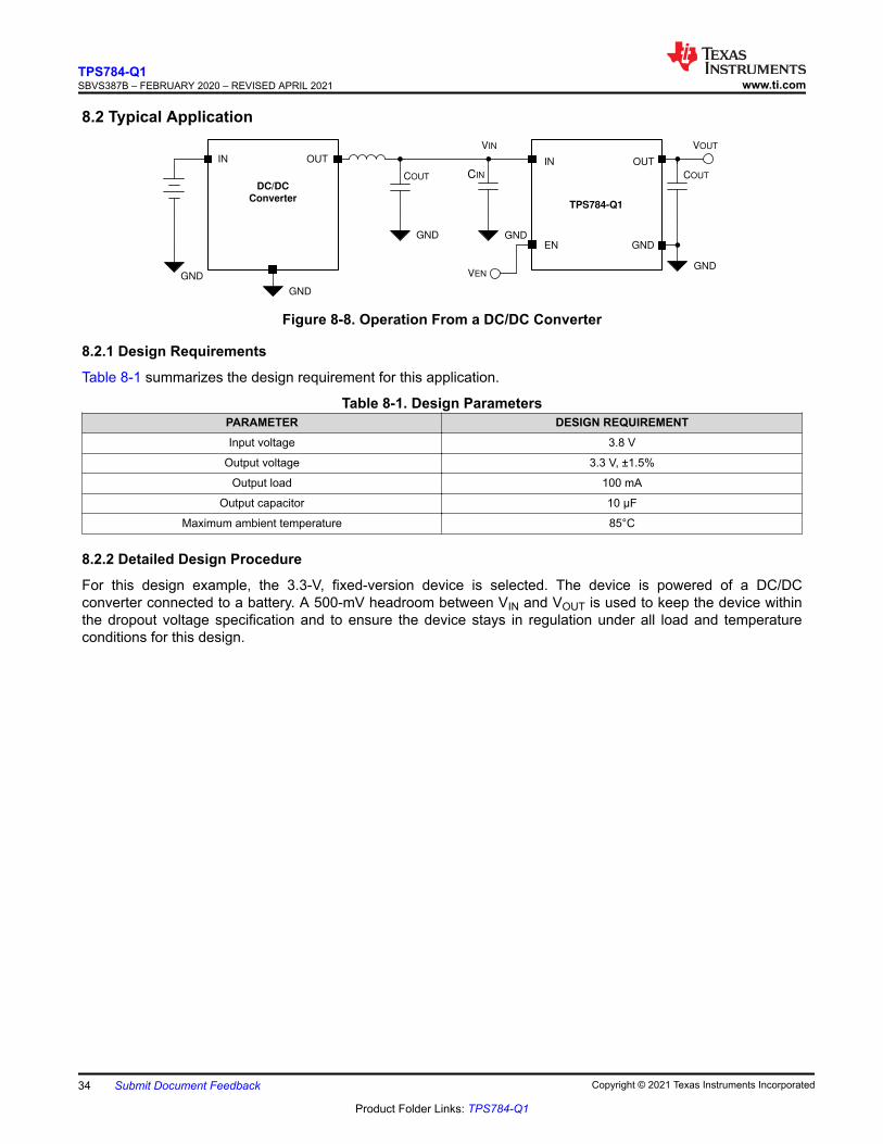
8.2 Typical Application
TPS784-Q1
IN
EN
OUT
GND
COUTCIN
DC/DC
Converter
IN OUT
COUT
VEN
GND GND
GND
GND
GND
VIN VOUT
Figure 8-8. Operation From a DC/DC Converter
8.2.1 Design Requirements
Table 8-1 summarizes the design requirement for this application.
Table 8-1. Design ParametersPARAMETER DESIGN REQUIREMENTInput voltage 3.8 V
Output voltage 3.3 V, ±1.5%
Output load 100 mA
Output capacitor 10 µF
Maximum ambient temperature 85°C
8.2.2 Detailed Design Procedure
For this design example, the 3.3-V, fixed-version device is selected. The device is powered of a DC/DCconverter connected to a battery. A 500-mV headroom between VIN and VOUT is used to keep the device withinthe dropout voltage specification and to ensure the device stays in regulation under all load and temperatureconditions for this design.
TPS784-Q1SBVS387B – FEBRUARY 2020 – REVISED APRIL 2021 www.ti.com
34 Submit Document Feedback Copyright © 2021 Texas Instruments Incorporated
Product Folder Links: TPS784-Q1

8.2.3 Application Curves
A 10-µF capacitor is used to reduce overshoot and undershoot of output voltage during load transients withramps rates greater than 0.5 A/µs. Figure 8-9 and Figure 8-10 show captures of load transient behavior for thisapplication.
Time (Ps)
AC
-Co
up
led
Ou
tpu
t V
olta
ge
(m
V)
Ou
tpu
t C
urr
en
t (m
A)
0 50 100 150 200 250 300 350 400 450 500-50 0
-40 100
-30 200
-20 300
-10 400
0 500
10 600
20 700
30 800
40 900
50 1000VOUT
IOUT
VIN = 3.8 V, VOUT = 3.3 V, COUT = 10 µF,IOUT slew rate = 1 A/µs
Figure 8-9. IOUT Transient From 0 mA to 100 mA
Time (Ps)
AC
-Co
up
led
Ou
tpu
t V
olta
ge
(m
V)
Ou
tpu
t C
urr
en
t (m
A)
0 100 200 300 400 500 600 700 800 900 1000-50 0
-40 100
-30 200
-20 300
-10 400
0 500
10 600
20 700
30 800
40 900
50 1000VOUT
IOUT
VIN = 3.8 V, VOUT = 3.3 V, COUT = 10 µF,IOUT slew rate = 1 A/µs
Figure 8-10. IOUT Transient From 1 mA to 100 mA
9 Power Supply RecommendationsThis device is designed to operate from an input supply voltage range of 1.65 V to 6.0 V. The input supply mustbe well regulated and free of spurious noise. To ensure that the output voltage is well regulated and dynamicperformance is optimum, the input supply must be at least VOUT(nom) + 0.5 V. TI requires using a 1-µF or greaterinput capacitor to reduce the impedance of the input supply, especially during transients.
www.ti.comTPS784-Q1
SBVS387B – FEBRUARY 2020 – REVISED APRIL 2021
Copyright © 2021 Texas Instruments Incorporated Submit Document Feedback 35
Product Folder Links: TPS784-Q1

10 Layout10.1 Layout Guidelines• Place input and output capacitors as close to the device as possible.• Use copper planes for device connections in order to optimize thermal performance.• Place thermal vias around the device to distribute the heat.• Only place tented thermal vias directly beneath the thermal pad of the DRB package. An untented via can
wick solder or solder paste away from the thermal pad joint during the soldering process, leading to acompromised solder joint on the thermal pad.
10.1.1 Additional Layout Considerations
The high impedance of the FB pin makes the regulator sensitive to parasitic capacitances that may coupleundesirable signals from nearby components (especially from logic and digital devices, such as microcontrollersand microprocessors); these capacitively-coupled signals may produce undesirable output voltage transients. Inthese cases, TI recommends using a fixed-voltage version of the device, or isolating the FB node by placing acopper ground plane on the layer directly underneath the LDO circuitry and FB pin to minimize any undesirablesignal coupling.
PCB Copper Area (cm�)
Ju
nctio
n-t
o-a
mb
ien
t th
erm
al re
sis
tan
ce
(RTJA)
(qC
/W)
0 20 40 60 80 10020
30
40
50
60
70
80
90
100
1101oz PCB2oz PCB
4-layer PCB
Figure 10-1. Junction-to-Ambient ThermalResistance (RθJA) vs PCB Copper Area
PCB Copper Area (cm�)
Ju
nctio
n-t
o-a
mb
ien
t th
erm
al re
sis
tan
ce
(RTJA)
(qC
/W)
0 20 40 60 80 10020
30
40
50
60
70
80
90
100
1101oz PCB2oz PCB
2-layer PCB
Figure 10-2. Junction-to-Ambient ThermalResistance (RθJA) vs PCB Copper Area
PCB Cuppoer Area (cm�)
Jun
ctio
n-t
o-b
oa
rd c
ha
ract
eriza
tion
pa
ram
ete
r (\
JB)
(qC
/W)
0 20 40 60 80 10015
20
25
30
35
401oz PCB2oz PCB
4-layer PCB
Figure 10-3. Junction-to-Board CharacterizationParameter (ψJB) vs PCB Copper Area
PCB Copper Area (cm�)
Jun
ctio
n-t
o-b
oa
rd c
ha
ract
eriza
tion
pa
ram
ete
r (\
JB)
(qC
/W)
0 10 20 30 40 50 60 70 80 90 10015
20
25
30
35
401oz PCB2oz PCB
2-layer PCB
Figure 10-4. Junction-to-Board CharacterizationParameter (ψJB) vs PCB Copper Area
TPS784-Q1SBVS387B – FEBRUARY 2020 – REVISED APRIL 2021 www.ti.com
36 Submit Document Feedback Copyright © 2021 Texas Instruments Incorporated
Product Folder Links: TPS784-Q1

10.2 Layout Examples
1
GND PLANE
COUT
2
3
4
8
7
6
5
CIN
OUT IN
NC
NC
NC
GND
ENFB
Represents a thermal via
R1
R2
CFF
Figure 10-5. Layout Example for the DRB PackageAdjustable Version
1
GND PLANE
COUT
2
3
4
8
7
6
5
CIN
OUT IN
NC
NC
NC
GND
ENNC
Represents a thermal via
Figure 10-6. Layout Example for the DRB PackageFixed Version
1
GND PLANE
CIN
2
3
5
4
COUT
FB
55
5
5 5
OUTIN
EN
GND R1 CFF
R2
Figure 10-7. Layout Example for the DBV PackageAdjustable Version
1
GND PLANE
CIN
2
3
5
4
COUT
NC
55
5
5 5
OUTIN
EN
GND
Figure 10-8. Layout Example for the DBV PackageFixed Version
www.ti.comTPS784-Q1
SBVS387B – FEBRUARY 2020 – REVISED APRIL 2021
Copyright © 2021 Texas Instruments Incorporated Submit Document Feedback 37
Product Folder Links: TPS784-Q1

11 Device and Documentation Support11.1 Device Support11.1.1 Device Nomenclature
Table 11-1. Device NomenclaturePRODUCT(1) (2) VOUT
TPS784xx(x)Pyyyz
xx(x) is the nominal output voltage. For output voltages with a resolution of 100 mV, two digits are usedin the ordering number; otherwise, three digits are used (for example, 28 = 2.8 V).P indicates an active output discharge feature. All members of the TPS784-Q1 family actively dischargethe output when the device is disabled.yyy is the package designator.z is the package quantity. R is for reel (3000 pieces), T is for tape (250 pieces).
(1) For the most current package and ordering information see the Package Option Addendum at the end of this document, or visit thedevice product folder on www.ti.com.
(2) Output voltages from 0.65 V to 5.5 V in 50-mV increments are available. Contact the factory for details and availability.
11.2 Documentation Support11.2.1 Related Documentation
For related documentation see the following:• Texas Instruments, Universal Low-Dropout (LDO) Linear Voltage Regulator MultiPkgLDOEVM-823 Evaluation
Module user's guide• Texas Instruments, Pros and Cons of Using a Feedforward Capacitor with a Low-Dropout Regulator
application report• Texas Instruments, An empirical analysis of the impact of board layout on LDO thermal performance
application report
11.3 Receiving Notification of Documentation UpdatesTo receive notification of documentation updates, navigate to the device product folder on ti.com. Click onSubscribe to updates to register and receive a weekly digest of any product information that has changed. Forchange details, review the revision history included in any revised document.
11.4 Support ResourcesTI E2E™ support forums are an engineer's go-to source for fast, verified answers and design help — straightfrom the experts. Search existing answers or ask your own question to get the quick design help you need.
Linked content is provided "AS IS" by the respective contributors. They do not constitute TI specifications and donot necessarily reflect TI's views; see TI's Terms of Use.
11.5 TrademarksTI E2E™ is a trademark of Texas Instruments.All trademarks are the property of their respective owners.11.6 Electrostatic Discharge Caution
This integrated circuit can be damaged by ESD. Texas Instruments recommends that all integrated circuits be handledwith appropriate precautions. Failure to observe proper handling and installation procedures can cause damage.ESD damage can range from subtle performance degradation to complete device failure. Precision integrated circuits maybe more susceptible to damage because very small parametric changes could cause the device not to meet its publishedspecifications.
11.7 GlossaryTI Glossary This glossary lists and explains terms, acronyms, and definitions.
TPS784-Q1SBVS387B – FEBRUARY 2020 – REVISED APRIL 2021 www.ti.com
38 Submit Document Feedback Copyright © 2021 Texas Instruments Incorporated
Product Folder Links: TPS784-Q1

12 Mechanical, Packaging, and Orderable InformationThe following pages include mechanical, packaging, and orderable information. This information is the mostcurrent data available for the designated devices. This data is subject to change without notice and revision ofthis document. For browser-based versions of this data sheet, refer to the left-hand navigation.
www.ti.comTPS784-Q1
SBVS387B – FEBRUARY 2020 – REVISED APRIL 2021
Copyright © 2021 Texas Instruments Incorporated Submit Document Feedback 39
Product Folder Links: TPS784-Q1

PACKAGE OPTION ADDENDUM
www.ti.com 20-Aug-2021
Addendum-Page 1
PACKAGING INFORMATION
Orderable Device Status(1)
Package Type PackageDrawing
Pins PackageQty
Eco Plan(2)
Lead finish/Ball material
(6)
MSL Peak Temp(3)
Op Temp (°C) Device Marking(4/5)
Samples
TPS78401QDBVRQ1 ACTIVE SOT-23 DBV 5 3000 RoHS & Green NIPDAU Level-2-260C-1 YEAR -40 to 150 23JF
TPS78401QWDRBRQ1 ACTIVE SON DRB 8 3000 RoHS & Green NIPDAU Level-2-260C-1 YEAR -40 to 150 8401WQ
TPS784075QWDRBRQ1 ACTIVE SON DRB 8 3000 RoHS & Green NIPDAU Level-2-260C-1 YEAR -40 to 150 84075W
TPS78408QDBVRQ1 ACTIVE SOT-23 DBV 5 3000 RoHS & Green NIPDAU Level-2-260C-1 YEAR -40 to 150 2BGF
TPS784105QWDRBRQ1 ACTIVE SON DRB 8 3000 RoHS & Green NIPDAU Level-2-260C-1 YEAR -40 to 150 84105W
TPS78410QWDRBRQ1 ACTIVE SON DRB 8 3000 RoHS & Green NIPDAU Level-2-260C-1 YEAR -40 to 150 8410WQ
TPS78411QWDRBRQ1 ACTIVE SON DRB 8 3000 RoHS & Green NIPDAU Level-2-260C-1 YEAR -40 to 150 8411WQ
TPS78412QDBVRQ1 ACTIVE SOT-23 DBV 5 3000 RoHS & Green NIPDAU Level-2-260C-1 YEAR -40 to 150 23KF
TPS78412QWDRBRQ1 ACTIVE SON DRB 8 3000 RoHS & Green NIPDAU Level-2-260C-1 YEAR -40 to 150 8412WQ
TPS78415QDBVRQ1 ACTIVE SOT-23 DBV 5 3000 RoHS & Green NIPDAU Level-2-260C-1 YEAR -40 to 150 23LF
TPS78415QWDRBRQ1 ACTIVE SON DRB 8 3000 RoHS & Green NIPDAU Level-2-260C-1 YEAR -40 to 150 8415WQ
TPS78417QDBVRQ1 ACTIVE SOT-23 DBV 5 3000 RoHS & Green NIPDAU Level-2-260C-1 YEAR -40 to 150 2BHF
TPS78418QDBVRQ1 ACTIVE SOT-23 DBV 5 3000 RoHS & Green NIPDAU Level-2-260C-1 YEAR -40 to 150 23MF
TPS78418QWDRBRQ1 ACTIVE SON DRB 8 3000 RoHS & Green NIPDAU Level-2-260C-1 YEAR -40 to 150 8418WQ
TPS78425QDBVRQ1 ACTIVE SOT-23 DBV 5 3000 RoHS & Green NIPDAU Level-2-260C-1 YEAR -40 to 150 23NF
TPS78425QWDRBRQ1 ACTIVE SON DRB 8 3000 RoHS & Green NIPDAU Level-2-260C-1 YEAR -40 to 150 8425WQ
TPS78428QDBVRQ1 ACTIVE SOT-23 DBV 5 3000 RoHS & Green NIPDAU Level-2-260C-1 YEAR -40 to 150 23OF
TPS78429QDBVRQ1 ACTIVE SOT-23 DBV 5 3000 RoHS & Green NIPDAU Level-2-260C-1 YEAR -40 to 150 23PF
TPS78430QDBVRQ1 ACTIVE SOT-23 DBV 5 3000 RoHS & Green NIPDAU Level-2-260C-1 YEAR -40 to 150 23QF
TPS78430QWDRBRQ1 ACTIVE SON DRB 8 3000 RoHS & Green NIPDAU Level-2-260C-1 YEAR -40 to 150 8430WQ

PACKAGE OPTION ADDENDUM
www.ti.com 20-Aug-2021
Addendum-Page 2
Orderable Device Status(1)
Package Type PackageDrawing
Pins PackageQty
Eco Plan(2)
Lead finish/Ball material
(6)
MSL Peak Temp(3)
Op Temp (°C) Device Marking(4/5)
Samples
TPS78433QDBVRQ1 ACTIVE SOT-23 DBV 5 3000 RoHS & Green NIPDAU Level-2-260C-1 YEAR -40 to 150 23RF
TPS78433QWDRBRQ1 ACTIVE SON DRB 8 3000 RoHS & Green NIPDAU Level-2-260C-1 YEAR -40 to 150 8433WQ
TPS78450QDBVRQ1 ACTIVE SOT-23 DBV 5 3000 RoHS & Green NIPDAU Level-2-260C-1 YEAR -40 to 150 2BIF
TPS78450QWDRBRQ1 ACTIVE SON DRB 8 3000 RoHS & Green NIPDAU Level-2-260C-1 YEAR -40 to 150 8450WQ
(1) The marketing status values are defined as follows:ACTIVE: Product device recommended for new designs.LIFEBUY: TI has announced that the device will be discontinued, and a lifetime-buy period is in effect.NRND: Not recommended for new designs. Device is in production to support existing customers, but TI does not recommend using this part in a new design.PREVIEW: Device has been announced but is not in production. Samples may or may not be available.OBSOLETE: TI has discontinued the production of the device.
(2) RoHS: TI defines "RoHS" to mean semiconductor products that are compliant with the current EU RoHS requirements for all 10 RoHS substances, including the requirement that RoHS substancedo not exceed 0.1% by weight in homogeneous materials. Where designed to be soldered at high temperatures, "RoHS" products are suitable for use in specified lead-free processes. TI mayreference these types of products as "Pb-Free".RoHS Exempt: TI defines "RoHS Exempt" to mean products that contain lead but are compliant with EU RoHS pursuant to a specific EU RoHS exemption.Green: TI defines "Green" to mean the content of Chlorine (Cl) and Bromine (Br) based flame retardants meet JS709B low halogen requirements of <=1000ppm threshold. Antimony trioxide basedflame retardants must also meet the <=1000ppm threshold requirement.
(3) MSL, Peak Temp. - The Moisture Sensitivity Level rating according to the JEDEC industry standard classifications, and peak solder temperature.
(4) There may be additional marking, which relates to the logo, the lot trace code information, or the environmental category on the device.
(5) Multiple Device Markings will be inside parentheses. Only one Device Marking contained in parentheses and separated by a "~" will appear on a device. If a line is indented then it is a continuationof the previous line and the two combined represent the entire Device Marking for that device.
(6) Lead finish/Ball material - Orderable Devices may have multiple material finish options. Finish options are separated by a vertical ruled line. Lead finish/Ball material values may wrap to twolines if the finish value exceeds the maximum column width.
Important Information and Disclaimer:The information provided on this page represents TI's knowledge and belief as of the date that it is provided. TI bases its knowledge and belief on informationprovided by third parties, and makes no representation or warranty as to the accuracy of such information. Efforts are underway to better integrate information from third parties. TI has taken andcontinues to take reasonable steps to provide representative and accurate information but may not have conducted destructive testing or chemical analysis on incoming materials and chemicals.TI and TI suppliers consider certain information to be proprietary, and thus CAS numbers and other limited information may not be available for release.

PACKAGE OPTION ADDENDUM
www.ti.com 20-Aug-2021
Addendum-Page 3
In no event shall TI's liability arising out of such information exceed the total purchase price of the TI part(s) at issue in this document sold by TI to Customer on an annual basis.
OTHER QUALIFIED VERSIONS OF TPS784-Q1 :
• Catalog : TPS784
NOTE: Qualified Version Definitions:
• Catalog - TI's standard catalog product

TAPE AND REEL INFORMATION
*All dimensions are nominal
Device PackageType
PackageDrawing
Pins SPQ ReelDiameter
(mm)
ReelWidth
W1 (mm)
A0(mm)
B0(mm)
K0(mm)
P1(mm)
W(mm)
Pin1Quadrant
TPS78401QDBVRQ1 SOT-23 DBV 5 3000 180.0 8.4 3.2 3.2 1.4 4.0 8.0 Q3
TPS78408QDBVRQ1 SOT-23 DBV 5 3000 180.0 8.4 3.2 3.2 1.4 4.0 8.0 Q3
TPS78412QDBVRQ1 SOT-23 DBV 5 3000 180.0 8.4 3.2 3.2 1.4 4.0 8.0 Q3
TPS78415QDBVRQ1 SOT-23 DBV 5 3000 180.0 8.4 3.2 3.2 1.4 4.0 8.0 Q3
TPS78417QDBVRQ1 SOT-23 DBV 5 3000 180.0 8.4 3.2 3.2 1.4 4.0 8.0 Q3
TPS78418QDBVRQ1 SOT-23 DBV 5 3000 180.0 8.4 3.2 3.2 1.4 4.0 8.0 Q3
TPS78425QDBVRQ1 SOT-23 DBV 5 3000 180.0 8.4 3.2 3.2 1.4 4.0 8.0 Q3
TPS78428QDBVRQ1 SOT-23 DBV 5 3000 180.0 8.4 3.2 3.2 1.4 4.0 8.0 Q3
TPS78429QDBVRQ1 SOT-23 DBV 5 3000 180.0 8.4 3.2 3.2 1.4 4.0 8.0 Q3
TPS78430QDBVRQ1 SOT-23 DBV 5 3000 180.0 8.4 3.2 3.2 1.4 4.0 8.0 Q3
TPS78433QDBVRQ1 SOT-23 DBV 5 3000 180.0 8.4 3.2 3.2 1.4 4.0 8.0 Q3
TPS78450QDBVRQ1 SOT-23 DBV 5 3000 180.0 8.4 3.2 3.2 1.4 4.0 8.0 Q3
PACKAGE MATERIALS INFORMATION
www.ti.com 8-Apr-2021
Pack Materials-Page 1
*All dimensions are nominal
Device Package Type Package Drawing Pins SPQ Length (mm) Width (mm) Height (mm)
TPS78401QDBVRQ1 SOT-23 DBV 5 3000 210.0 185.0 35.0
TPS78408QDBVRQ1 SOT-23 DBV 5 3000 210.0 185.0 35.0
TPS78412QDBVRQ1 SOT-23 DBV 5 3000 210.0 185.0 35.0
TPS78415QDBVRQ1 SOT-23 DBV 5 3000 210.0 185.0 35.0
TPS78417QDBVRQ1 SOT-23 DBV 5 3000 210.0 185.0 35.0
TPS78418QDBVRQ1 SOT-23 DBV 5 3000 210.0 185.0 35.0
TPS78425QDBVRQ1 SOT-23 DBV 5 3000 210.0 185.0 35.0
TPS78428QDBVRQ1 SOT-23 DBV 5 3000 210.0 185.0 35.0
TPS78429QDBVRQ1 SOT-23 DBV 5 3000 210.0 185.0 35.0
TPS78430QDBVRQ1 SOT-23 DBV 5 3000 210.0 185.0 35.0
TPS78433QDBVRQ1 SOT-23 DBV 5 3000 210.0 185.0 35.0
TPS78450QDBVRQ1 SOT-23 DBV 5 3000 210.0 185.0 35.0
PACKAGE MATERIALS INFORMATION
www.ti.com 8-Apr-2021
Pack Materials-Page 2

www.ti.com
PACKAGE OUTLINE
C
0.220.08 TYP
0.25
3.02.6
2X 0.95
1.9
1.450.90
0.150.00 TYP
5X 0.50.3
0.60.3 TYP
80 TYP
1.9
A
3.052.75
B1.751.45
(1.1)
SOT-23 - 1.45 mm max heightDBV0005ASMALL OUTLINE TRANSISTOR
4214839/F 06/2021
NOTES: 1. All linear dimensions are in millimeters. Any dimensions in parenthesis are for reference only. Dimensioning and tolerancing per ASME Y14.5M.2. This drawing is subject to change without notice.3. Refernce JEDEC MO-178.4. Body dimensions do not include mold flash, protrusions, or gate burrs. Mold flash, protrusions, or gate burrs shall not exceed 0.25 mm per side.
0.2 C A B
1
34
5
2
INDEX AREAPIN 1
GAGE PLANE
SEATING PLANE
0.1 C
SCALE 4.000
www.ti.com
EXAMPLE BOARD LAYOUT
0.07 MAXARROUND
0.07 MINARROUND
5X (1.1)
5X (0.6)
(2.6)
(1.9)
2X (0.95)
(R0.05) TYP
4214839/F 06/2021
SOT-23 - 1.45 mm max heightDBV0005ASMALL OUTLINE TRANSISTOR
NOTES: (continued) 5. Publication IPC-7351 may have alternate designs. 6. Solder mask tolerances between and around signal pads can vary based on board fabrication site.
SYMM
LAND PATTERN EXAMPLEEXPOSED METAL SHOWN
SCALE:15X
PKG
1
3 4
5
2
SOLDER MASKOPENINGMETAL UNDER
SOLDER MASK
SOLDER MASKDEFINED
EXPOSED METAL
METALSOLDER MASKOPENING
NON SOLDER MASKDEFINED
(PREFERRED)
SOLDER MASK DETAILS
EXPOSED METAL

www.ti.com
EXAMPLE STENCIL DESIGN
(2.6)
(1.9)
2X(0.95)
5X (1.1)
5X (0.6)
(R0.05) TYP
SOT-23 - 1.45 mm max heightDBV0005ASMALL OUTLINE TRANSISTOR
4214839/F 06/2021
NOTES: (continued) 7. Laser cutting apertures with trapezoidal walls and rounded corners may offer better paste release. IPC-7525 may have alternate design recommendations. 8. Board assembly site may have different recommendations for stencil design.
SOLDER PASTE EXAMPLEBASED ON 0.125 mm THICK STENCIL
SCALE:15X
SYMM
PKG
1
3 4
5
2


NOTES:
1. All linear dimensions are in millimeters. Any dimensions in parenthesis are for reference only. Dimensioning and tolerancingper ASME Y14.5M.
2. This drawing is subject to change without notice.3. The package thermal pad must be soldered to the printed circuit board for optimal thermal and mechanical performance.
PACKAGE OUTLINE
4225036/A 06/2019
www.ti.com
VSON - 1 mm max height
PLASTIC QUAD FLAT PACK- NO LEAD
DRB0008J
A
0.08 C
0.1 C A B0.05 C
B
SYMM
SYMM
PIN 1 INDEX AREA
3.12.9
3.12.9
1 MAX
0.050.00
SEATING PLANE
C
SECTION A-ATYPICAL
(0.13)
0.1 MIN
1.751.55
(0.2) TYP
(0.19)
8X 0.360.26
2.52.3
6X 0.65
1.95
8X 0.50.3
PIN 1 ID(OPTIONAL)
1
4
8
5
9
AutoCAD SHX Text
AutoCAD SHX Text

NOTES: (continued)
4. This package is designed to be soldered to a thermal pad on the board. For more information, see Texas Instruments literaturenumber SLUA271 (www.ti.com/lit/slua271).
5. Vias are optional depending on application, refer to device data sheet. If any vias are implemented, refer to their locations shown on this view. It is recommended that vias under paste be filled, plugged or tented.
EXAMPLE BOARD LAYOUT
4225036/A 06/2019
www.ti.com
VSON - 1 mm max height
DRB0008J
PLASTIC QUAD FLAT PACK- NO LEAD
SYMM
SYMM
LAND PATTERN EXAMPLEEXPOSED METAL SHOWN
SCALE: 20X
SOLDER MASK DETAILS
NON- SOLDER MASKDEFINED
(PREFERRED)
SOLDER MASKDEFINED
0.07 MAXALL AROUND
EXPOSED METAL
METAL
SOLDER MASKOPENING
0.07 MINALL AROUND
EXPOSED METAL
SOLDER MASKOPENING
METAL
(1.65)
(2.4)
(2.8)
(0.95)
(0.575)
8X (0.6)
8X (0.31)
6X (0.65)
(1.95)
1
9
45
8
(R0.05) TYP
(Ø 0.2) VIATYP
AutoCAD SHX Text
AutoCAD SHX Text

NOTES: (continued)
6. Laser cutting apertures with trapezoidal walls and rounded corners may offer better paste release. IPC-7525 may have alternatedesign recommendations.
EXAMPLE STENCIL DESIGN
4225036/A 06/2019
www.ti.com
VSON - 1 mm max height
DRB0008J
PLASTIC QUAD FLAT PACK- NO LEAD
SOLDER PASTE EXAMPLEBASED ON 0.125 mm THICK STENCIL
EXPOSED PAD81% PRINTED COVERAGE BY AREA
SCALE: 20X
SYMM
SYMM
2X(1.51)
2X(1.06)
(2.8)
(0.63)
8X (0.6)
8X (0.31)
6X (0.65)
(1.95)
1
45
8
(R0.05) TYP9
METALTYP
AutoCAD SHX Text
AutoCAD SHX Text
IMPORTANT NOTICE AND DISCLAIMERTI PROVIDES TECHNICAL AND RELIABILITY DATA (INCLUDING DATASHEETS), DESIGN RESOURCES (INCLUDING REFERENCEDESIGNS), APPLICATION OR OTHER DESIGN ADVICE, WEB TOOLS, SAFETY INFORMATION, AND OTHER RESOURCES “AS IS”AND WITH ALL FAULTS, AND DISCLAIMS ALL WARRANTIES, EXPRESS AND IMPLIED, INCLUDING WITHOUT LIMITATION ANYIMPLIED WARRANTIES OF MERCHANTABILITY, FITNESS FOR A PARTICULAR PURPOSE OR NON-INFRINGEMENT OF THIRDPARTY INTELLECTUAL PROPERTY RIGHTS.These resources are intended for skilled developers designing with TI products. You are solely responsible for (1) selecting the appropriateTI products for your application, (2) designing, validating and testing your application, and (3) ensuring your application meets applicablestandards, and any other safety, security, or other requirements. These resources are subject to change without notice. TI grants youpermission to use these resources only for development of an application that uses the TI products described in the resource. Otherreproduction and display of these resources is prohibited. No license is granted to any other TI intellectual property right or to any third partyintellectual property right. TI disclaims responsibility for, and you will fully indemnify TI and its representatives against, any claims, damages,costs, losses, and liabilities arising out of your use of these resources.TI’s products are provided subject to TI’s Terms of Sale (https:www.ti.com/legal/termsofsale.html) or other applicable terms available eitheron ti.com or provided in conjunction with such TI products. TI’s provision of these resources does not expand or otherwise alter TI’sapplicable warranties or warranty disclaimers for TI products.IMPORTANT NOTICE
Mailing Address: Texas Instruments, Post Office Box 655303, Dallas, Texas 75265Copyright © 2021, Texas Instruments Incorporated


