TPS65090EVM User's Guide (Rev. A) - TI.com
27
User's Guide SLVU778A – October 2012 – Revised January 2013 TPS65090EVM User's Guide This guide details the use of the TPS65090 evaluation module, TPS65090EVM (referred to as EVM for the remainder of this document). The TPS65090, front-end power management unit (PMU), is an integrated high-input voltage (6 V–17 V) charger and power path management device including 3 step-down converters, 2 low-dropout regulators (LDO), 7 load-switches, 16-channel 10-bit A/D converter and I 2 C™ interface. The EVM facilitates evaluation of the integrated circuit (IC) and serves as a reference design. For more information on the TPS65090, refer to the datasheet: TPS65090 High Input Voltage Frontend PMU for Mobile Computer,(SLVSAU3). Contents 1 Requirements ................................................................................................................ 2 2 Setup and Operation ....................................................................................................... 2 2.1 Power Connections ................................................................................................ 2 3 Headers and Jumpers ...................................................................................................... 3 4 Graphical User Interface (GUI) ............................................................................................ 4 5 Schematic Diagram ......................................................................................................... 4 6 Board Layout ................................................................................................................ 9 7 Bill of Materials ............................................................................................................. 16 8 References ................................................................................................................. 18 List of Figures 1 TPS65090EVM GUI ........................................................................................................ 4 2 TPS65090EVM Schematic Charger or Power Path and Configuration .............................................. 5 3 TPS65090EVM Schematic Converters and Load Switches ........................................................... 6 4 TPS65090EVM Schematic USB to I 2 C Interface ....................................................................... 7 5 TPS65090EVM Schematic Test Pads ................................................................................... 8 6 TPS65090EVM Board Layout, Top Assembly .......................................................................... 9 7 TPS65090EVM Board Layout, Bottom Assembly (mirrored) ........................................................ 10 8 TPS65090EVM Board Layout, Top ..................................................................................... 11 9 TPS65090EVM Board Layout, Internal 2............................................................................... 12 10 TPS65090EVM Board Layout, Internal 3............................................................................... 13 11 TPS65090EVM Board Layout, Bottom (mirrored) ..................................................................... 14 12 TPS65090EVM Board Layout, Top Silkscreen ........................................................................ 15 List of Tables 1 EVM Header and Jumper Descriptions .................................................................................. 3 2 TPS65090 Solution, Required Components ........................................................................... 16 3 TPS65090EVM Evaluation Components ............................................................................... 17 Windows is a registered trademark of Microsoft Corporation. I 2 C is a trademark of NXP. 1 SLVU778A – October 2012 – Revised January 2013 TPS65090EVM User's Guide Submit Documentation Feedback Copyright © 2012–2013, Texas Instruments Incorporated
Transcript of TPS65090EVM User's Guide (Rev. A) - TI.com

User's GuideSLVU778A–October 2012–Revised January 2013
TPS65090EVM User's Guide
This guide details the use of the TPS65090 evaluation module, TPS65090EVM (referred to as EVM forthe remainder of this document).
The TPS65090, front-end power management unit (PMU), is an integrated high-input voltage (6 V–17 V)charger and power path management device including 3 step-down converters, 2 low-dropout regulators(LDO), 7 load-switches, 16-channel 10-bit A/D converter and I2C™ interface.
The EVM facilitates evaluation of the integrated circuit (IC) and serves as a reference design. For moreinformation on the TPS65090, refer to the datasheet: TPS65090 High Input Voltage Frontend PMU forMobile Computer, (SLVSAU3).
Contents1 Requirements ................................................................................................................ 22 Setup and Operation ....................................................................................................... 2
2.1 Power Connections ................................................................................................ 23 Headers and Jumpers ...................................................................................................... 34 Graphical User Interface (GUI) ............................................................................................ 45 Schematic Diagram ......................................................................................................... 46 Board Layout ................................................................................................................ 97 Bill of Materials ............................................................................................................. 168 References ................................................................................................................. 18
List of Figures
1 TPS65090EVM GUI ........................................................................................................ 4
2 TPS65090EVM Schematic Charger or Power Path and Configuration.............................................. 5
3 TPS65090EVM Schematic Converters and Load Switches........................................................... 6
4 TPS65090EVM Schematic USB to I2C Interface ....................................................................... 7
5 TPS65090EVM Schematic Test Pads ................................................................................... 8
6 TPS65090EVM Board Layout, Top Assembly .......................................................................... 9
7 TPS65090EVM Board Layout, Bottom Assembly (mirrored) ........................................................ 10
8 TPS65090EVM Board Layout, Top ..................................................................................... 11
9 TPS65090EVM Board Layout, Internal 2............................................................................... 12
10 TPS65090EVM Board Layout, Internal 3............................................................................... 13
11 TPS65090EVM Board Layout, Bottom (mirrored)..................................................................... 14
12 TPS65090EVM Board Layout, Top Silkscreen ........................................................................ 15
List of Tables
1 EVM Header and Jumper Descriptions .................................................................................. 3
2 TPS65090 Solution, Required Components ........................................................................... 16
3 TPS65090EVM Evaluation Components ............................................................................... 17
Windows is a registered trademark of Microsoft Corporation.I2C is a trademark of NXP.
1SLVU778A–October 2012–Revised January 2013 TPS65090EVM User's GuideSubmit Documentation Feedback
Copyright © 2012–2013, Texas Instruments Incorporated

Requirements www.ti.com
WARNINGEXPORT NOTICE:
Recipient agrees to not knowingly export or re-export, directly orindirectly, any product or technical data (as defined by the U.S.,EU, and other Export Administration Regulations) includingsoftware, or any controlled product restricted by other applicablenational regulations, received from Disclosing party under thisAgreement, or any direct product of such technology, to anydestination to which such export or re-export is restricted orprohibited by U.S. or other applicable laws, without obtaining priorauthorization from U.S. Department of Commerce and othercompetent Government authorities to the extent required by thoselaws. This provision shall survive termination or expiration of thisAgreement. According to our best knowledge of the state and end-use of this product or technology, and in compliance with theexport control regulations of dual-use goods in force in the originand exporting countries, this technology is classified as follows:
US ECCN: 3E991
EU ECCN: EAR99
And may require export or re-export license for shipping it incompliance with the applicable regulations of certain countries.
1 Requirements
In order to use the EVM, a lab power supply capable of supplying at least the TPS65090 output power ata voltage between 6 V and 17 V and/or a rechargeable multi-cell lithium battery is required. Additionally, acomputer running Windows® 7 or Windows XP loaded with the TPS65090EVM-SW graphical userinterface (GUI) and a mini-USB cable are recommended.
2 Setup and Operation
2.1 Power Connections
Connect the lab power supply to the input labeled AC (AC adapter), J1; pin 1 positive lead and pin 6negative lead.
Connect the rechargeable Li-Ion battery to J3; pin 1 positive lead and pin 6 negative lead.
By default, the charger and converters are enabled and disabled by external pins. The LDOs are alwayson, since they additionally provide power to internal blocks.
2 TPS65090EVM User's Guide SLVU778A–October 2012–Revised January 2013Submit Documentation Feedback
Copyright © 2012–2013, Texas Instruments Incorporated

www.ti.com Headers and Jumpers
3 Headers and Jumpers
Many of the 6-pin headers provide Kelvin sense lines, S+ and S– (pins 3 and 4), for sensing the voltagedirectly at the input or output capacitors.
Table 1. EVM Header and Jumper Descriptions
Reference Name DescriptionDesignator
J1 V_AC Input connection for AC adapter
J2 VSYS Header for power path output system voltage
J3 V_BAT Header for Li-Ion battery connection
J4 DCDC1 Header for output voltage of switching converter, DCDC1
J5 DCDC2 Header for output voltage of switching converter, DCDC2
J6 DCDC3 Header for output voltage of switching converter, DCDC3
J7 Digital Header for open drain outputs, each pulled up to J14
J8 VIO Jumper to select pull-up for I2C bus, default: USB_3P3
J9 USB_3P3 Header for output of U4, 5-V to 3.3-V LDO
J10 I2C Header for I2C bus
J11 J11 Mini-USB connection to PC for GUI
J12 SCL pull-Up Jumper to pull–up SCL to J8, default: installed
J13 SDA pull-Up Jumper to pull–up SDA to J8, default: installed
J14 Output pull-up Jumper to select pull-up for open-drain outputs
J15 ENC Jumper to externally enable or disable charger
J16 TS1 Header connection to pin TS1 network
J17 TS2 Header connection to pin TS2 network
J18 EN_DCDC1 Jumper to externally enable or disable DCDC1
J19 EN_DCDC2 Jumper to externally enable or disable DCDC2
J20 EN_DCDC3 Jumper to externally enable or disable DCDC3
J21 LDO1 Header to output voltage of LDO1
J22 LDO2 Header to output voltage of LDO2
J23 FET Out Header to FET outputs
J24 FET In Header to FET inputs
J25 Factory Use Jumper used for firmware install only
JP1 I_VSYS Solder bridge to optionally measure VSYS current
JP2 I_VBAT Solder bridge to optionally measure V_BAT inductor current
JP3 I1 Solder bridge to optionally measure DCDC1 inductor current
JP4 I2 Solder bridge to optionally measure DCDC2 inductor current
JP5 I3 Solder bridge to optionally measure DCDC3 inductor current
3SLVU778A–October 2012–Revised January 2013 TPS65090EVM User's GuideSubmit Documentation Feedback
Copyright © 2012–2013, Texas Instruments Incorporated

Graphical User Interface (GUI) www.ti.com
4 Graphical User Interface (GUI)
The GUI design allows the TPS65090 to easily interface with a PC. The GUI gives the capability to readand write the contents of the I2C registers and simplifies use with radio check boxes, drop-down menusand pushbuttons.
Figure 1. TPS65090EVM GUI
5 Schematic Diagram
The schematic diagram illustrates the circuit connections of the EVM.
This EVM contains many components that are not necessary for an end-product. These additionalcomponents are added to simplify evaluation of the IC. In Section 7, the Bill of Materials (BOM), there aretwo tables; the first table includes the required materials for functionality of the TPS65090 and the secondtable contains the additional materials added for evaluation.
4 TPS65090EVM User's Guide SLVU778A–October 2012–Revised January 2013Submit Documentation Feedback
Copyright © 2012–2013, Texas Instruments Incorporated

SCL
SDA
GND
GND
I²C Pull Up
Sense to C1
Sense to C5
GND
ENC
IRQ
VACG
VBATG
VSYSG
STAT
GND
PGND
PGND
USB_3P3
VIO_LDO2
VIO
LDO2
LDO1
LDO2
V_AC
V_AC
VSYS
VSYS
SENSE +
SENSE -
PGND
PGND
V_BAT
V_BAT
SENSE +
SENSE -
PGND
PGND
TS1
AGND
TS2
AGND
sense at R16
Op. 3 cell
R3 = 1100k
R4 = 220k
single
optionsensor
I_VSYS
I_VBAT
4A 4A
4A 10A
10A
10A4A/6Apk
VSYS
V_BAT
pla
ce p
art
sclo
se t
o Q
1
clo
se t
o I
C
All ground is connected at PowerPad
GN
D 0
GN
D 1
GN
D 0
GN
D 1
USB_3P3
GND
the option to split VCTRL and VPROGOTP using R44 is only required to connect higher OTP programming voltage
1 Components without a value are not installed
Batt
ery
Charg
er
CN
TRL
A50 ACN
B47 ACP
B48 ACS
A51 ACG
A14 VACS
A13 VAC
B13 STAT
B36 VSYSG
A38 VBATG
A39 VACG
A41 ENC
A27 SDATB25 SCLK
B12 IRQ
B35 VREF
B39 VCTRL
B26 VREFADC
A28 VPROGOTP
A33 AGNDA40 GND 105PWPD
C4PGND
C3PGND
C2PGND
C1PGND
B6PGNDC
A6PGNDC
B23TS2
A24TS1
A25VREFT
A52FBC
B1SRN
A1SRP
B5LC
A5LC
B4LC
B2CBC
A15VBAT
A2BATG
A4VSYSC
B3VSYSC
A3VSYSC
U1-A
TPS65090RVN
TPS65090RVN
L1
2.2 uH
G
S D
Q2CSD17304Q3
G
SD
Q1CSD17304Q3
C1
1uF
C2
10uF
C3
10uF
C44700pF
C5
1uF
C6
10uF
C7
10uF
R2
0.01
R52.2k R6
2.2k
R76.8k
R86.8k
4
5
1 2 3
Q3CSD25401Q3
R1
0.01
1
2
3
4
5
6
J1
1
2
3
4
5
6
J2
1
2
3
4
5
6
J3
Q4BSS138W-7-FD1
1N
4148W
-7-F
1
2
3
4
J10
1
2
3
J8
J12 J13
1
2
3
J14
C35
2.2uF
C37
100nF
1
2
3
J15
R2010k
R2110k
1
2
J16
1
2
J17
R38
1M
C54
1uF
R39
JP2
R42
R43
JP1
TP1 TP2
TP3
TP4
TP5 TP6
TP7
TP8
TP10
TP11TP12
TP13
TP14
TP15TP16TP17
1
2
3
4
5
6
J7
J9
SH1 SH2
C36
2.2uF
R9
10k
R10
10k
R11
10k
R12
10k
R4
110k
R15
1M
R18
1k
R19
1k
R14
3M
R3
330k
R44 0
R17
10k
R13
0.002
C55
100nF
C56
100nF
C57
100nF
C58
100nFC59
100nF
C60
100nF
C61
100nF
C62
100nF
C63
100nF
C64
1uF
C65
100nF
C66
100nF
R47 4.7k
R48 4.7k
C67
100nF
R49
470k
TP9
R45
3.9
R46
3.9
R5010
R16
10k
1
1
1
1
SDASCL
SCL
SDA
VOUT_LDO2
VOUT_LDO1
VOUT_LDO2
VOUT_LDO2
VSYS
VSYSC
VCTRL
VPROGOTP
IRQ
VIO
VACG
VBATG
VSYSG
STAT
V_AC
VIO_PUP
SDA_PUP
SCL_PUP
ENC
TS1
TS2
VSYS
USB_3P3
V_BAT
www.ti.com Schematic Diagram
Figure 2. TPS65090EVM Schematic Charger or Power Path and Configuration
5SLVU778A–October 2012–Revised January 2013 TPS65090EVM User's GuideSubmit Documentation Feedback
Copyright © 2012–2013, Texas Instruments Incorporated

Sense to C11
Sense to C17
Sense to C23
Sense to C26
Sense to C27
DCD
C1 5
VD
CD
C2 3
.3V
DCD
C3 1
.35V
LD
O1 5
V
LD
O2 3
.3V
FET1_OUT
FET2_OUT
FET3_OUT
FET4_OUT
FET5_OUT
FET6_OUT
FET7_OUT
FET3_OUT
3A
1A
1A
1A
1A
FET1_IN
FET2_IN
FET3_IN
FET3_IN
FET4_IN
FET5_IN
FET6_IN
FET7_IN
EN_DCDC1
EN_DCDC2
EN_DCDC3
GND
V_LDO2
GND
V_LDO2
GND
V_LDO2
DCDC1
DCDC1
SENSE +
SENSE -
PGND
PGND
DCDC2
DCDC2
SENSE +
SENSE -
PGND
PGND
DCDC3
DCDC3
SENSE +
SENSE -
PGND
PGND
V_LDO1
V_LDO1
SENSE +
SENSE -
PGND
PGND
V_LDO2
V_LDO2
SENSE +
SENSE -
PGND
PGND
5A/6Apk
5A/6Apk
5A/6Apk
100mA
100mA
1A
200mA
5A/6Apk
5A/6Apk
100mA
100mA
5A/6Apk
17V
17V
3.3VI1
I2
I3
5.0V
3.3V
all 2.2uF close
to the IC
GN
D 2
GN
D 2
GN
D 3
GN
D 3
GN
D 4
GN
D 4
LD
O2
DCD
C1
LD
O1
DCD
C3
DCD
C2
A46 VSYS1B43 VSYS1A47 VSYS1
B38 EN1
A19 VSYS2B18 VSYS2A20 VSYS2
A42 EN2
A10 VSYS3A11 VSYS3B10 VSYS3B11 VSYS3
A26 EN3
A49 VSYS_L1
A17 VSYS_L2
B15FB_L2
B16VLDO2
B46FB_L1
B45VLDO1
A8PGND3
B7PGND3
A7PGND3
B14FB3
A16VDCDC3
B9L3
A9L3
B8L3
A12CB3
B22PGND2
B21PGND2
A22PGND2
A23PGND2
B24FB2
A18VDCDC2
B20L2
A21L2
B19L2
B17CB2
A44PGND1
B40PGND1
A43PGND1
B37FB1
A48VDCDC1
B42L1
A45L1
B41L1
B44CB1
U1-B
TPS65090RVN
TPS65090RVN
B28 INFET1
B29 INFET2
B31 INFET3
A34 INFET3
B34 INFET4
B33 INFET5
B32 INFET6
B27 INFET7 A29VEFT7
A35VFET6
A36VFET5
A37VFET4
A32VFET3
B30VFET3
A31VFET2
A30VFET1
U1-C
TPS65090RVN
TPS65090RVN
L2
2.2 uH
L3
2.2 uH
L4
2.2 uH
C8
1uF
C9
10uF
C104700pF
C11
2.2uF
C12
10uF
C13
10uF
C14
1uF
C15
10uF
C164700pF
C17
2.2uF
C18
10uF
C19
10uF
C20
1uF
C21
10uF
C224700pF
C23
2.2uF
C24
10uF
C25
10uF
C28
10uF25V
C29
10uF
C30
10uF
C31
10uF
C32
10uF
C33
10uF
C34
10uF
1
2
3
4
5
6
J4
1
2
3
4
5
6
J5
1
2
3
4
5
6
J6
1
2
3
J18
1
2
3
J19
1
2
3
J20
R22
1M
R23
1M
R24
1M
C38
1uF
C39
1uF
1
2
3
4
5
6
J21
1
2
3
4
5
6
J22
C46
10uF
C471uF
C482.2uF
C492.2uF
C502.2uF
C512.2uF
C522.2uF
C532.2uF
123456789
10111213141516
J23
R25 0
R26
R27
R28 0
R29
R30 0
R31
R32 0
R33
R34 0
R35
R36 0
12345678910111213141516
J24
R37 0
JP3
JP4
JP5
C26
10uF
C40
10uF
C41
10uF
C42
10uF
C43
10uF
C44
10uF
C45
10uF
R41
470k
R40
330k
C27
10uF
1
EN1
EN2
EN3
VSYSVOUT_LDO2
EN1
EN2
EN3
VOUT_LDO2 VOUT_LDO2
VSYS
VOUT_DCDC1
VOUT_DCDC2
VOUT_DCDC1
VOUT_DCDC2
VOUT_LDO1
INFET1
INFET2
INFET3
INFET4
INFET5
INFET6
INFET7
VFET1
VFET2
VFET3
VFET4
VFET5
VFET6
VFET7
VOUT_DCDC3
Schematic Diagram www.ti.com
Figure 3. TPS65090EVM Schematic Converters and Load Switches
6 TPS65090EVM User's Guide SLVU778A–October 2012–Revised January 2013Submit Documentation Feedback
Copyright © 2012–2013, Texas Instruments Incorporated

USB2I2C Interface
1P6.4/CB4/A4
2P6.5/CB5/A5
3P6.6/CB6/A6
4P6.7/CB7/A7
5P7.0/CB8/A12
6P7.1/CB9/A13
7P7.2/CB10/A14
8P7.3/CB11/A15
9P5.0/VREF+/VEREF+
10P5.1/VREF-/VEREF-
11AVCC1
12P5.4/XIN
13P5.5/XOUT
14AVSS1
15P8.0
16P8.1
17P8.2
18DVCC1
19DVSS1
20VCORE
21
P1.0
/TA0CLK/A
CLK
22
P1.1
/TA0.0
23
P1.2
/TA0.1
24
P1.3
/TA0.2
25
P1.4
/TA0.3
26
P1.5
/TA0.4
27
P1.6
/TA1CLK/C
BO
UT
28
P1.7
/TA1.0
29
P2.0
/TA1.1
30
P2.1
/TA1.2
31
P2.2
/TA2CLK/S
MCLK
32
P2.3
/TA2.0
33
P2.4
/TA2.1
34
P2.5
/TA2.2
35
P2.6
/RTCCLK/D
MAE0
36
P2.7
/UCB0/S
TEU
CA0CLK
37
P3.0
/UCB0SIM
O/U
CB0SD
38
P3.1
/UCB0SO
MI/
UCB0SC
39
P3.2
/UCB0CLK/U
CA0STE
40
P3,3
/UCA0TXD
/UCA0SIM
41P3.4/UCA0RXD/UCA0SOM
42P3.5/TB0.5
43P3.6/TB0.6
44P3.7/TB0OUTH/SVMOUT
45P4.0/PM_UCB1STE/PM_U
46P4.1/PM_UCB1SIMO
47P4.2/PM_UCB1SOMI
48P4.3/PM_UCB1CLK
49DVSS2
50DVCC2
51P4.4/PM_UCA1TXD
52P4.5/PM_UCA1RXD
53P4.6/PM_NONE
54P4.7/PM_NONE
55P5.6/TB0.0
56P5.7/TB0.1
57P7.4/TB0.2
58P7.5/TB0.3
59P7.6/TB0.4
60P7.7/TB0CLK/MCLK
61
VSSU
62
PU
.0/D
P
63
PU
R
64
PU
.1/D
M
65
VBU
S
66
VU
SB
67
V18
68
AVSS2
69
P5.2
/XT2IN
70
P5.3
/XT2O
UT
71
TEST/S
BW
TCK
72
PJ.
0/T
DO
73
PJ.
1/T
DI/
TCLK
74
PJ.
2/T
MS
75
PJ.
3/T
CK
76
NM
I/SBW
TD
IO/R
ST
77
P6.0
/CB0/A
0
78
P6.1
/CB1/A
1
79
P6.2
/CB2/A
2
80
P6.3
/CB3/A
3
U2
MSP430F552XIPN
MSP430F5529IPN
1IO
1
2IO
2
3G
ND
4IO
3
5IO
4
6VCC
U3
TPD
4E004D
RY
1OUT
2NC
3NR/FB
4GND
5EN
6NC
7NC
8IN
9
PWPD
U4
TPS73533DRB
V+
DM
DP
NC
V-
CASE
CASE
J11
L5
MI1206K900R-10
D2
1SMB5922BT3G
1 2
R51 33
1 2
R52
33
12
Y1
24.0
MH
z12
C6830pF
12
C6930pF
1 2
R53
33k
12
C70
C0603
0.1uF
12
C71
0.1uF
12
C72
C0603
0.1uF
C73
1uF 12
C74
0.01uF
1 2
R54
1.5k
1
2
R55
1.2M
J25
12
C75
220pF
12
C76
220pF
+
C77
22uF1
2
C78
470nF
1
2
R59
33k
12
C79
2.2
nF
12
C80
2.2uF
1 2
R57
0
1
USB_3P3
USB_3P3
USB_3P3
SDA
SCL
GND1PGND
www.ti.com Schematic Diagram
Figure 4. TPS65090EVM Schematic USB to I2C Interface
7SLVU778A–October 2012–Revised January 2013 TPS65090EVM User's GuideSubmit Documentation Feedback
Copyright © 2012–2013, Texas Instruments Incorporated

1
2
3
4
5
6
7
8
9
10
X1
1
2
3
4
5
6
7
8
9
10
X2
1
2
3
4
5
6
7
8
9
10
X3
1
2
3
4
5
6
7
8
9
10
X4
1
2
3
4
5
6
7
8
9
10
X5
1
2
3
4
5
6
7
8
9
10
X6
1
2
3
4
5
6
7
8
9
10
X7
1
2
3
4
5
6
7
8
9
10
X8
1
2
3
4
5
6
7
8
9
10
X10
1
2
3
4
5
6
7
8
9
10
X11
1
2
3
4
5
6
7
8
9
10
X9
AGND
EN1
EN2
EN3
ENC
GND1
GND1
GND1
GND1
INFET1
INFET2
INFET3
INFET3
INFET4
INFET5
INFET6
INFET7
IRQ
PWRGNDPWRGND
PWRGND
PWRGND
PWRGND
PWRGND
PWRGND
PWRGND
PWRGND
PWRGND
PWRGND
PWRGND
PWRGND
PWRGND
PWRGND
PWRGND
PWRGND
PWRGND
PWRGNDPWRGND
PWRGND
PWRGNDPWRGND
PWRGND
PWRGNDPWRGND
PWRGND
PWRGND
STAT
TS2
VACG
PWRGND
VBATG
VFET1
VFET2
VFET3
VFET3
VFET4
VFET5
VFET6
VFET7
VIO
USB_3P3
USB_3P3
VIO_PUP
VOUT_DCDC1
VOUT_DCDC1
VOUT_DCDC1
VOUT_DCDC2
VOUT_DCDC2
VOUT_DCDC2
VOUT_DCDC3
VOUT_DCDC3
VOUT_DCDC3
VOUT_LDO1
VOUT_LDO1
VOUT_LDO1
VOUT_LDO1
VOUT_LDO2
VOUT_LDO2
VOUT_LDO2
VOUT_LDO2
VOUT_LDO2
VOUT_LDO2
VOUT_LDO2
VSYS
VSYS
VSYSC
VSYSG
V_AC
V_AC
V_AC
V_BAT
V_BAT
V_BAT
AGND
GND1
SCL
SCL_PUP
SDA
SDA_PUP
TS1
VIO_PUP
VIO_PUP
VPROGOTP
VCTRL
Schematic Diagram www.ti.com
Figure 5. TPS65090EVM Schematic Test Pads
8 TPS65090EVM User's Guide SLVU778A–October 2012–Revised January 2013Submit Documentation Feedback
Copyright © 2012–2013, Texas Instruments Incorporated

1
1
1
1
+
1
1
1
C1
C10
C11
C14
C16 C17
C20
C22
C23
C35
C36
C37
C38
C39
C4
C47
C48
C49
C5
C50
C51
C52
C53
C8
C12
C13
C15
C18
C19
C2 C21
C24
C25
C28
C29
C3
C30
C31
C32
C33
C34
C46
C6
C7
C9
D1
J16
J17
J8
J14
J15
J18
J19
J20
J10
J1
J2
J21
J22
J3
J4
J5
J6
J23 J24
L1
L2 L3
L4
JP
1
JP
2
JP3 JP4
JP
5
J12
J13
R42
R43
R22
R23
R24
R38
R5
R6
R7
R8
R39
R1
R13
R2
R20
R21
Q4
Q1
Q2
Q3
AVT1
AVT2 AVT3
R25
R27
R29
R31
R33
R35
R37
R26
R28
R30
R32
R34
R36
C54
TP10
TP11
TP12
TP13
TP14TP2
TP3
TP4
TP5
TP6
TP8
TP9
TP16
TP17
TP1
TP15
J7
J9
U1
C26
C40
C41
C42
C43
C44
C45
R10
R11
R12
R15
R14
R17
R18
R19
R9
R4
R3 R
41
R40
R44
C64
R45
R46
R50
R16
C27
L5
C6
8
C69
C70
C71
C72
C7
4
C75
C76
C78
C79
C80
C73
C77
J11
Y1
D2
U2
R51
R52
R53
R54R55
R57
R59
U3
U4
J25
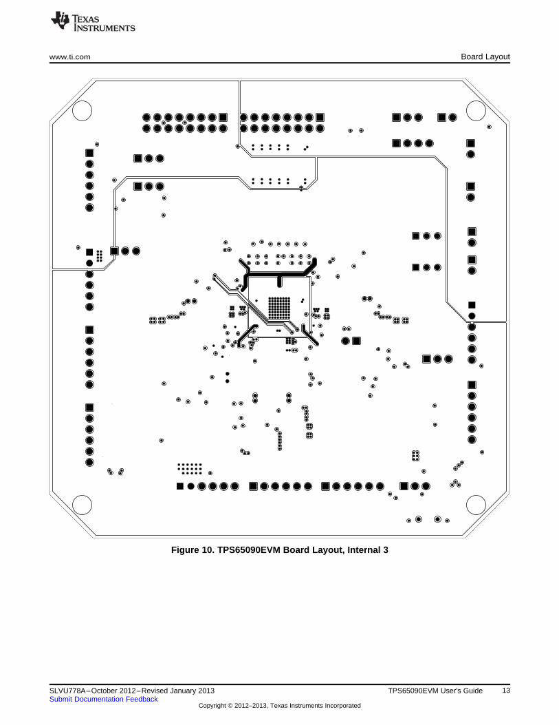
www.ti.com Board Layout
6 Board Layout
This section provides the EVM board layout and illustrations.
Board layout is critical for all high-frequency, switch-mode power supplies. The following figures show theboard layout for the EVM printed-circuit board. The nodes with high-switching frequencies and currentsare kept as short as possible to minimize trace inductance.
Careful attention has been given to the routing of high-frequency current loops and a single-pointgrounding scheme is used. See the data sheet for specific layout guidelines.
Figure 6. TPS65090EVM Board Layout, Top Assembly
9SLVU778A–October 2012–Revised January 2013 TPS65090EVM User's GuideSubmit Documentation Feedback
Copyright © 2012–2013, Texas Instruments Incorporated

8X1 1 X7 6 X1
X5
1X
41
X3
1
X211 X1
X9
11
X10
1X
11
Board Layout www.ti.com
Figure 7. TPS65090EVM Board Layout, Bottom Assembly (mirrored)
10 TPS65090EVM User's Guide SLVU778A–October 2012–Revised January 2013Submit Documentation Feedback
Copyright © 2012–2013, Texas Instruments Incorporated

www.ti.com Board Layout
Figure 8. TPS65090EVM Board Layout, Top
11SLVU778A–October 2012–Revised January 2013 TPS65090EVM User's GuideSubmit Documentation Feedback
Copyright © 2012–2013, Texas Instruments Incorporated

Board Layout www.ti.com
Figure 9. TPS65090EVM Board Layout, Internal 2
12 TPS65090EVM User's Guide SLVU778A–October 2012–Revised January 2013Submit Documentation Feedback
Copyright © 2012–2013, Texas Instruments Incorporated
www.ti.com Board Layout
Figure 10. TPS65090EVM Board Layout, Internal 3
13SLVU778A–October 2012–Revised January 2013 TPS65090EVM User's GuideSubmit Documentation Feedback
Copyright © 2012–2013, Texas Instruments Incorporated

Board Layout www.ti.com
Figure 11. TPS65090EVM Board Layout, Bottom (mirrored)
14 TPS65090EVM User's Guide SLVU778A–October 2012–Revised January 2013Submit Documentation Feedback
Copyright © 2012–2013, Texas Instruments Incorporated

1
1
1
1
+1
1
1
+
1
VSYS PWRGNDSense
V_BAT PWRGNDSense
DCDC3 PWRGNDSense
PW
RG
ND
LD
O2
Sense
PW
RG
ND
DC
DC
2
Sense
PW
RG
ND
V_A
CS
ense
PW
RG
ND
LD
O1
Sense
DC
DC
1P
WR
GN
D
Sense
SD
A
SC
L
GN
D1
GN
D1
BO
X
VIO
LD
O2
EN
2
LD
O
GN
D
EN
3
GN
D
LD
O
EN
1
LD
O
GN
D
EN
C
GN
D
LD
O1
LD
O2
VIO
STAT
VSYSG
VBATG
VACG
IRQ
GND1
1234567 3 1234567 3
FE
TO
UT
FE
TIN
LD
O2
C1
C10
C11
C1
4
C16
C1
7
C20C22
C23
C3
5
C36
C3
7C
38
C3
9
C4
C4
7
C4
8
C4
9
C5
C5
0
C5
1
C5
2
C5
3
C8C12
C13
C15
C18
C19
C2C21
C24C25
C28
C29
C3
C30
C31
C32
C33
C34
C46
C6C7
C9
D1
J16
J17
J8
J14
J15
J18
J19
J20
J10
J1
J2
J21
J22
J3
J4
J5
J6
J23 J24
L1
L2L3
L4
JP1
JP2
JP3JP4
JP5
J12
J13
R42
R43
R22
R23
R2
4
R38
R5
R6
R7
R8
R39
R1
R13
R2
R20
R21
Q4
Q1
Q2
Q3
R25
R27
R29
R31
R33
R35
R37
R26
R28
R30
R32
R34
R36
C54
TP10
TP11
TP12
TP13
TP14
TP2
TP3
TP4
TP
5
TP6
TP7
TP
8
TP9
TP16
TP17
TP1
TP15
J7
J9
U1
C2
6
C40
C41
C42
C43
C44
C45
R10
R11
R12
R15
R14
R17
R9
R4
R3
R41
R40
R44
C55
C56
C57
C58
C59
C60
C61
C62
C63
C65 C66
C64
C67
R47
R48
R49
R45 R46 R50
R16
C2
7
L5
C73
C77
J11
Y1
D2
U2
U3
U4
J25
www.ti.com Board Layout
Figure 12. TPS65090EVM Board Layout, Top Silkscreen
15SLVU778A–October 2012–Revised January 2013 TPS65090EVM User's GuideSubmit Documentation Feedback
Copyright © 2012–2013, Texas Instruments Incorporated
Bill of Materials www.ti.com
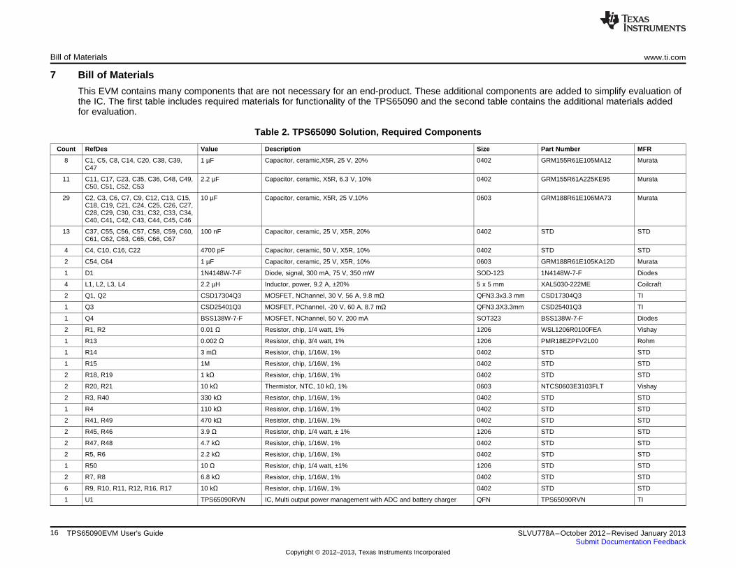
7 Bill of Materials
This EVM contains many components that are not necessary for an end-product. These additional components are added to simplify evaluation ofthe IC. The first table includes required materials for functionality of the TPS65090 and the second table contains the additional materials addedfor evaluation.
Table 2. TPS65090 Solution, Required Components
Count RefDes Value Description Size Part Number MFR
8 C1, C5, C8, C14, C20, C38, C39, 1 µF Capacitor, ceramic,X5R, 25 V, 20% 0402 GRM155R61E105MA12 MurataC47
11 C11, C17, C23, C35, C36, C48, C49, 2.2 µF Capacitor, ceramic, X5R, 6.3 V, 10% 0402 GRM155R61A225KE95 MurataC50, C51, C52, C53
29 C2, C3, C6, C7, C9, C12, C13, C15, 10 µF Capacitor, ceramic, X5R, 25 V,10% 0603 GRM188R61E106MA73 MurataC18, C19, C21, C24, C25, C26, C27,C28, C29, C30, C31, C32, C33, C34,C40, C41, C42, C43, C44, C45, C46
13 C37, C55, C56, C57, C58, C59, C60, 100 nF Capacitor, ceramic, 25 V, X5R, 20% 0402 STD STDC61, C62, C63, C65, C66, C67
4 C4, C10, C16, C22 4700 pF Capacitor, ceramic, 50 V, X5R, 10% 0402 STD STD
2 C54, C64 1 µF Capacitor, ceramic, 25 V, X5R, 10% 0603 GRM188R61E105KA12D Murata
1 D1 1N4148W-7-F Diode, signal, 300 mA, 75 V, 350 mW SOD-123 1N4148W-7-F Diodes
4 L1, L2, L3, L4 2.2 µH Inductor, power, 9.2 A, ±20% 5 x 5 mm XAL5030-222ME Coilcraft
2 Q1, Q2 CSD17304Q3 MOSFET, NChannel, 30 V, 56 A, 9.8 mΩ QFN3.3x3.3 mm CSD17304Q3 TI
1 Q3 CSD25401Q3 MOSFET, PChannel, -20 V, 60 A, 8.7 mΩ QFN3.3X3.3mm CSD25401Q3 TI
1 Q4 BSS138W-7-F MOSFET, NChannel, 50 V, 200 mA SOT323 BSS138W-7-F Diodes
2 R1, R2 0.01 Ω Resistor, chip, 1/4 watt, 1% 1206 WSL1206R0100FEA Vishay
1 R13 0.002 Ω Resistor, chip, 3/4 watt, 1% 1206 PMR18EZPFV2L00 Rohm
1 R14 3 mΩ Resistor, chip, 1/16W, 1% 0402 STD STD
1 R15 1M Resistor, chip, 1/16W, 1% 0402 STD STD
2 R18, R19 1 kΩ Resistor, chip, 1/16W, 1% 0402 STD STD
2 R20, R21 10 kΩ Thermistor, NTC, 10 kΩ, 1% 0603 NTCS0603E3103FLT Vishay
2 R3, R40 330 kΩ Resistor, chip, 1/16W, 1% 0402 STD STD
1 R4 110 kΩ Resistor, chip, 1/16W, 1% 0402 STD STD
2 R41, R49 470 kΩ Resistor, chip, 1/16W, 1% 0402 STD STD
2 R45, R46 3.9 Ω Resistor, chip, 1/4 watt, ± 1% 1206 STD STD
2 R47, R48 4.7 kΩ Resistor, chip, 1/16W, 1% 0402 STD STD
2 R5, R6 2.2 kΩ Resistor, chip, 1/16W, 1% 0402 STD STD
1 R50 10 Ω Resistor, chip, 1/4 watt, ±1% 1206 STD STD
2 R7, R8 6.8 kΩ Resistor, chip, 1/16W, 1% 0402 STD STD
6 R9, R10, R11, R12, R16, R17 10 kΩ Resistor, chip, 1/16W, 1% 0402 STD STD
1 U1 TPS65090RVN IC, Multi output power management with ADC and battery charger QFN TPS65090RVN TI
16 TPS65090EVM User's Guide SLVU778A–October 2012–Revised January 2013Submit Documentation Feedback
Copyright © 2012–2013, Texas Instruments Incorporated

www.ti.com Bill of Materials
Table 3. TPS65090EVM Evaluation Components
Count RefDes Value Description Size Part Number MFR
2 C68, C69 30 pF Capacitor, ceramic, 50 V, C0G, 10% 0603 STD STD
3 C70, C71, C72 0.1 µF Capacitor, ceramic, 16 V, X7R, 10% 0603 STD STD
1 C73 1 µF Capacitor, ceramic chip, 10 V, ±10% 0805 STD STD
1 C74 0.01 µF Capacitor, ceramic, 16 V, X7R, 10% 0603 STD STD
2 C75, C76 220 pF Capacitor, ceramic, 50 V, C0G, 5% 0603 STD STD
1 C77 22 µF Capacitor, alum. 10 VDC, ±20% 6032 EEE-1AA220WR Panasonic
1 C78 470 nF Capacitor, ceramic, 16 V, X7R, 10% 0603 STD STD
1 C79 2.2 nF Capacitor, ceramic, 25 V, X7R, 20% 0603 STD STD
1 C80 2.2 µF Capacitor, ceramic, 10 V, X7R, 10% 0603 STD STD
1 D2 1SMB5922BT3G Diode, Zener, 7.5 V, 50 mA, 3 W SMB 1SMB5922BT3G On Semi
9 J1–J6, J21, J22, J7 PEC06SAAN Header, male 6 pin, 100-mil spacing, 0.100 in × 6 PEC06SAAN Sullins
1 J10 PEC04SAAN Header, male 4 pin, 100-mil spacing, 0.100 in × 4 PEC04SAAN Sullins
1 J11 1734035-2 Connector, recpt, USB-B, mini, 5 pins, SMT 0.354 × 0.400 in 1734035-2
2 J23, J24 PEC08DAAN Header, male 2x8 pin, 100-mil spacing 0.100 in × 2 × 8 PEC08DAAN Sullins
6 J8, J14, J15, J18–J20 PEC03SAAN Header, male 3-pin, 100-mil spacing, 0.100 in × 3 PEC03SAAN Sullins
6 J9, J12, J13, J16, J17, J25 PEC02SAAN Header, male 2 pin, 100-mil spacing 0.100 in × 2 PEC02SAAN Sullins
1 L5 MI1206K900R-10 Bead, ferrite, SMT, 90 Ω, 1.5A 1206 MI1206K900R-10 Laird
4 R22, R23, R24, R38 1M Resistor, chip, 1/16W, 1% 0402 STD STD
2 R20, R21 10 kΩ Thermistor, NTC, 10 kΩ, 1% 0603 NTCS0603E3103FLT Vishay
9 R25, R28, R30, R32, R34, 0 Ω Resistor, chip, 1/16W, 1% 0603 STD STDR36, R37, R44, R57
0 R26, R27, R29, R31, R33, R35 0 Ω Resistor, chip, 1/16W, 1% 0603 STD STD
0 R39 0 Ω Resistor, chip, 1/16W, 0.1% 0603 STD STD
0 R42, R43 50 kΩ Potentiometer, single slide, 50 kΩ, 0.1 W, 20% 0.378 × 0.217 in Copal
2 R51, R52 33 Ω Resistor, chip, 1/16W, 1% 0603 Std Std
2 R53, R59 33 kΩ Resistor, chip, 1/16W, 1% 0603 Std Std
1 R54 1.5 kΩ Resistor, chip, 1/16W, 1% 0603 Std Std
1 R55 1.2 MΩ Resistor, chip, 1/16W, 1% 0603 Std Std
1 U2 MSP430F5529IPN IC, mixed signal microcontroller TQFP-80 MSP430F5529IPN TI
1 U3 TPD4E004DRY IC, 4-chan ESD-protection array SON-6 TPD4E004DRY TI
1 U4 TPS73533DRB IC, 500 mA, low quiescent current, ultra-low noise, high PSRR LDO, 3.3 SON-8 TPS73533DRB TIV
1 Y1 24.0 MHz Crystal, SMT quartz crystal 0.484 × 0.190 in ECS-240-20-5PX-TR CTS
1 -- PCB, 4.2 in × 4.2 in × 0.062 in PWR108 Any
17SLVU778A–October 2012–Revised January 2013 TPS65090EVM User's GuideSubmit Documentation Feedback
Copyright © 2012–2013, Texas Instruments Incorporated

References www.ti.com
8 References1. TPS65090 High Input Voltage Frontend PMU for Mobile Computer, (SLVSAU3)
18 TPS65090EVM User's Guide SLVU778A–October 2012–Revised January 2013Submit Documentation Feedback
Copyright © 2012–2013, Texas Instruments Incorporated

EVALUATION BOARD/KIT/MODULE (EVM) ADDITIONAL TERMS
Texas Instruments (TI) provides the enclosed Evaluation Board/Kit/Module (EVM) under the following conditions:
The user assumes all responsibility and liability for proper and safe handling of the goods. Further, the user indemnifies TI from all claimsarising from the handling or use of the goods.
Should this evaluation board/kit not meet the specifications indicated in the User’s Guide, the board/kit may be returned within 30 days fromthe date of delivery for a full refund. THE FOREGOING LIMITED WARRANTY IS THE EXCLUSIVE WARRANTY MADE BY SELLER TOBUYER AND IS IN LIEU OF ALL OTHER WARRANTIES, EXPRESSED, IMPLIED, OR STATUTORY, INCLUDING ANY WARRANTY OFMERCHANTABILITY OR FITNESS FOR ANY PARTICULAR PURPOSE. EXCEPT TO THE EXTENT OF THE INDEMNITY SET FORTHABOVE, NEITHER PARTY SHALL BE LIABLE TO THE OTHER FOR ANY INDIRECT, SPECIAL, INCIDENTAL, OR CONSEQUENTIALDAMAGES.
Please read the User's Guide and, specifically, the Warnings and Restrictions notice in the User's Guide prior to handling the product. Thisnotice contains important safety information about temperatures and voltages. For additional information on TI's environmental and/or safetyprograms, please visit www.ti.com/esh or contact TI.
No license is granted under any patent right or other intellectual property right of TI covering or relating to any machine, process, orcombination in which such TI products or services might be or are used. TI currently deals with a variety of customers for products, andtherefore our arrangement with the user is not exclusive. TI assumes no liability for applications assistance, customer product design,software performance, or infringement of patents or services described herein.
REGULATORY COMPLIANCE INFORMATION
As noted in the EVM User’s Guide and/or EVM itself, this EVM and/or accompanying hardware may or may not be subject to the FederalCommunications Commission (FCC) and Industry Canada (IC) rules.
For EVMs not subject to the above rules, this evaluation board/kit/module is intended for use for ENGINEERING DEVELOPMENT,DEMONSTRATION OR EVALUATION PURPOSES ONLY and is not considered by TI to be a finished end product fit for general consumeruse. It generates, uses, and can radiate radio frequency energy and has not been tested for compliance with the limits of computingdevices pursuant to part 15 of FCC or ICES-003 rules, which are designed to provide reasonable protection against radio frequencyinterference. Operation of the equipment may cause interference with radio communications, in which case the user at his own expense willbe required to take whatever measures may be required to correct this interference.
General Statement for EVMs including a radio
User Power/Frequency Use Obligations: This radio is intended for development/professional use only in legally allocated frequency andpower limits. Any use of radio frequencies and/or power availability of this EVM and its development application(s) must comply with locallaws governing radio spectrum allocation and power limits for this evaluation module. It is the user’s sole responsibility to only operate thisradio in legally acceptable frequency space and within legally mandated power limitations. Any exceptions to this are strictly prohibited andunauthorized by Texas Instruments unless user has obtained appropriate experimental/development licenses from local regulatoryauthorities, which is responsibility of user including its acceptable authorization.
For EVMs annotated as FCC – FEDERAL COMMUNICATIONS COMMISSION Part 15 Compliant
Caution
This device complies with part 15 of the FCC Rules. Operation is subject to the following two conditions: (1) This device may not causeharmful interference, and (2) this device must accept any interference received, including interference that may cause undesired operation.
Changes or modifications not expressly approved by the party responsible for compliance could void the user's authority to operate theequipment.
FCC Interference Statement for Class A EVM devices
This equipment has been tested and found to comply with the limits for a Class A digital device, pursuant to part 15 of the FCC Rules.These limits are designed to provide reasonable protection against harmful interference when the equipment is operated in a commercialenvironment. This equipment generates, uses, and can radiate radio frequency energy and, if not installed and used in accordance with theinstruction manual, may cause harmful interference to radio communications. Operation of this equipment in a residential area is likely tocause harmful interference in which case the user will be required to correct the interference at his own expense.

FCC Interference Statement for Class B EVM devices
This equipment has been tested and found to comply with the limits for a Class B digital device, pursuant to part 15 of the FCC Rules.These limits are designed to provide reasonable protection against harmful interference in a residential installation. This equipmentgenerates, uses and can radiate radio frequency energy and, if not installed and used in accordance with the instructions, may causeharmful interference to radio communications. However, there is no guarantee that interference will not occur in a particular installation. Ifthis equipment does cause harmful interference to radio or television reception, which can be determined by turning the equipment off andon, the user is encouraged to try to correct the interference by one or more of the following measures:
• Reorient or relocate the receiving antenna.• Increase the separation between the equipment and receiver.• Connect the equipment into an outlet on a circuit different from that to which the receiver is connected.• Consult the dealer or an experienced radio/TV technician for help.
For EVMs annotated as IC – INDUSTRY CANADA Compliant
This Class A or B digital apparatus complies with Canadian ICES-003.
Changes or modifications not expressly approved by the party responsible for compliance could void the user’s authority to operate theequipment.
Concerning EVMs including radio transmitters
This device complies with Industry Canada licence-exempt RSS standard(s). Operation is subject to the following two conditions: (1) thisdevice may not cause interference, and (2) this device must accept any interference, including interference that may cause undesiredoperation of the device.
Concerning EVMs including detachable antennas
Under Industry Canada regulations, this radio transmitter may only operate using an antenna of a type and maximum (or lesser) gainapproved for the transmitter by Industry Canada. To reduce potential radio interference to other users, the antenna type and its gain shouldbe so chosen that the equivalent isotropically radiated power (e.i.r.p.) is not more than that necessary for successful communication.
This radio transmitter has been approved by Industry Canada to operate with the antenna types listed in the user guide with the maximumpermissible gain and required antenna impedance for each antenna type indicated. Antenna types not included in this list, having a gaingreater than the maximum gain indicated for that type, are strictly prohibited for use with this device.
Cet appareil numérique de la classe A ou B est conforme à la norme NMB-003 du Canada.
Les changements ou les modifications pas expressément approuvés par la partie responsable de la conformité ont pu vider l’autorité del'utilisateur pour actionner l'équipement.
Concernant les EVMs avec appareils radio
Le présent appareil est conforme aux CNR d'Industrie Canada applicables aux appareils radio exempts de licence. L'exploitation estautorisée aux deux conditions suivantes : (1) l'appareil ne doit pas produire de brouillage, et (2) l'utilisateur de l'appareil doit accepter toutbrouillage radioélectrique subi, même si le brouillage est susceptible d'en compromettre le fonctionnement.
Concernant les EVMs avec antennes détachables
Conformément à la réglementation d'Industrie Canada, le présent émetteur radio peut fonctionner avec une antenne d'un type et d'un gainmaximal (ou inférieur) approuvé pour l'émetteur par Industrie Canada. Dans le but de réduire les risques de brouillage radioélectrique àl'intention des autres utilisateurs, il faut choisir le type d'antenne et son gain de sorte que la puissance isotrope rayonnée équivalente(p.i.r.e.) ne dépasse pas l'intensité nécessaire à l'établissement d'une communication satisfaisante.
Le présent émetteur radio a été approuvé par Industrie Canada pour fonctionner avec les types d'antenne énumérés dans le manueld’usage et ayant un gain admissible maximal et l'impédance requise pour chaque type d'antenne. Les types d'antenne non inclus danscette liste, ou dont le gain est supérieur au gain maximal indiqué, sont strictement interdits pour l'exploitation de l'émetteur.
SPACER
SPACER
SPACER
SPACER
SPACER
SPACER
SPACER
SPACER

【【Important Notice for Users of this Product in Japan】】This development kit is NOT certified as Confirming to Technical Regulations of Radio Law of Japan
If you use this product in Japan, you are required by Radio Law of Japan to follow the instructions below with respect to this product:
1. Use this product in a shielded room or any other test facility as defined in the notification #173 issued by Ministry of Internal Affairs andCommunications on March 28, 2006, based on Sub-section 1.1 of Article 6 of the Ministry’s Rule for Enforcement of Radio Law ofJapan,
2. Use this product only after you obtained the license of Test Radio Station as provided in Radio Law of Japan with respect to thisproduct, or
3. Use of this product only after you obtained the Technical Regulations Conformity Certification as provided in Radio Law of Japan withrespect to this product. Also, please do not transfer this product, unless you give the same notice above to the transferee. Please notethat if you could not follow the instructions above, you will be subject to penalties of Radio Law of Japan.
Texas Instruments Japan Limited(address) 24-1, Nishi-Shinjuku 6 chome, Shinjuku-ku, Tokyo, Japan
http://www.tij.co.jp
【ご使用にあたっての注】
本開発キットは技術基準適合証明を受けておりません。
本製品のご使用に際しては、電波法遵守のため、以下のいずれかの措置を取っていただく必要がありますのでご注意ください。1. 電波法施行規則第6条第1項第1号に基づく平成18年3月28日総務省告示第173号で定められた電波暗室等の試験設備でご使用いただく。2. 実験局の免許を取得後ご使用いただく。3. 技術基準適合証明を取得後ご使用いただく。
なお、本製品は、上記の「ご使用にあたっての注意」を譲渡先、移転先に通知しない限り、譲渡、移転できないものとします。
上記を遵守頂けない場合は、電波法の罰則が適用される可能性があることをご留意ください。
日本テキサス・インスツルメンツ株式会社東京都新宿区西新宿6丁目24番1号西新宿三井ビルhttp://www.tij.co.jp
SPACER
SPACER
SPACER
SPACER
SPACER
SPACER
SPACER
SPACER
SPACER
SPACER
SPACER
SPACER
SPACER
SPACER
SPACER
SPACER
EVALUATION BOARD/KIT/MODULE (EVM)WARNINGS, RESTRICTIONS AND DISCLAIMERS
For Feasibility Evaluation Only, in Laboratory/Development Environments. Unless otherwise indicated, this EVM is not a finishedelectrical equipment and not intended for consumer use. It is intended solely for use for preliminary feasibility evaluation inlaboratory/development environments by technically qualified electronics experts who are familiar with the dangers and application risksassociated with handling electrical mechanical components, systems and subsystems. It should not be used as all or part of a finished endproduct.
Your Sole Responsibility and Risk. You acknowledge, represent and agree that:
1. You have unique knowledge concerning Federal, State and local regulatory requirements (including but not limited to Food and DrugAdministration regulations, if applicable) which relate to your products and which relate to your use (and/or that of your employees,affiliates, contractors or designees) of the EVM for evaluation, testing and other purposes.
2. You have full and exclusive responsibility to assure the safety and compliance of your products with all such laws and other applicableregulatory requirements, and also to assure the safety of any activities to be conducted by you and/or your employees, affiliates,contractors or designees, using the EVM. Further, you are responsible to assure that any interfaces (electronic and/or mechanical)between the EVM and any human body are designed with suitable isolation and means to safely limit accessible leakage currents tominimize the risk of electrical shock hazard.
3. You will employ reasonable safeguards to ensure that your use of the EVM will not result in any property damage, injury or death, evenif the EVM should fail to perform as described or expected.
4. You will take care of proper disposal and recycling of the EVM’s electronic components and packing materials.
Certain Instructions. It is important to operate this EVM within TI’s recommended specifications and environmental considerations per theuser guidelines. Exceeding the specified EVM ratings (including but not limited to input and output voltage, current, power, andenvironmental ranges) may cause property damage, personal injury or death. If there are questions concerning these ratings please contacta TI field representative prior to connecting interface electronics including input power and intended loads. Any loads applied outside of thespecified output range may result in unintended and/or inaccurate operation and/or possible permanent damage to the EVM and/orinterface electronics. Please consult the EVM User's Guide prior to connecting any load to the EVM output. If there is uncertainty as to theload specification, please contact a TI field representative. During normal operation, some circuit components may have case temperaturesgreater than 60°C as long as the input and output are maintained at a normal ambient operating temperature. These components includebut are not limited to linear regulators, switching transistors, pass transistors, and current sense resistors which can be identified using theEVM schematic located in the EVM User's Guide. When placing measurement probes near these devices during normal operation, pleasebe aware that these devices may be very warm to the touch. As with all electronic evaluation tools, only qualified personnel knowledgeablein electronic measurement and diagnostics normally found in development environments should use these EVMs.
Agreement to Defend, Indemnify and Hold Harmless. You agree to defend, indemnify and hold TI, its licensors and their representativesharmless from and against any and all claims, damages, losses, expenses, costs and liabilities (collectively, "Claims") arising out of or inconnection with any use of the EVM that is not in accordance with the terms of the agreement. This obligation shall apply whether Claimsarise under law of tort or contract or any other legal theory, and even if the EVM fails to perform as described or expected.
Safety-Critical or Life-Critical Applications. If you intend to evaluate the components for possible use in safety critical applications (suchas life support) where a failure of the TI product would reasonably be expected to cause severe personal injury or death, such as deviceswhich are classified as FDA Class III or similar classification, then you must specifically notify TI of such intent and enter into a separateAssurance and Indemnity Agreement.
Mailing Address: Texas Instruments, Post Office Box 655303, Dallas, Texas 75265Copyright © 2013, Texas Instruments Incorporated

STANDARD TERMS AND CONDITIONS FOR EVALUATION MODULES1. Delivery: TI delivers TI evaluation boards, kits, or modules, including any accompanying demonstration software, components, or
documentation (collectively, an “EVM” or “EVMs”) to the User (“User”) in accordance with the terms and conditions set forth herein.Acceptance of the EVM is expressly subject to the following terms and conditions.1.1 EVMs are intended solely for product or software developers for use in a research and development setting to facilitate feasibility
evaluation, experimentation, or scientific analysis of TI semiconductors products. EVMs have no direct function and are notfinished products. EVMs shall not be directly or indirectly assembled as a part or subassembly in any finished product. Forclarification, any software or software tools provided with the EVM (“Software”) shall not be subject to the terms and conditionsset forth herein but rather shall be subject to the applicable terms and conditions that accompany such Software
1.2 EVMs are not intended for consumer or household use. EVMs may not be sold, sublicensed, leased, rented, loaned, assigned,or otherwise distributed for commercial purposes by Users, in whole or in part, or used in any finished product or productionsystem.
2 Limited Warranty and Related Remedies/Disclaimers:2.1 These terms and conditions do not apply to Software. The warranty, if any, for Software is covered in the applicable Software
License Agreement.2.2 TI warrants that the TI EVM will conform to TI's published specifications for ninety (90) days after the date TI delivers such EVM
to User. Notwithstanding the foregoing, TI shall not be liable for any defects that are caused by neglect, misuse or mistreatmentby an entity other than TI, including improper installation or testing, or for any EVMs that have been altered or modified in anyway by an entity other than TI. Moreover, TI shall not be liable for any defects that result from User's design, specifications orinstructions for such EVMs. Testing and other quality control techniques are used to the extent TI deems necessary or asmandated by government requirements. TI does not test all parameters of each EVM.
2.3 If any EVM fails to conform to the warranty set forth above, TI's sole liability shall be at its option to repair or replace such EVM,or credit User's account for such EVM. TI's liability under this warranty shall be limited to EVMs that are returned during thewarranty period to the address designated by TI and that are determined by TI not to conform to such warranty. If TI elects torepair or replace such EVM, TI shall have a reasonable time to repair such EVM or provide replacements. Repaired EVMs shallbe warranted for the remainder of the original warranty period. Replaced EVMs shall be warranted for a new full ninety (90) daywarranty period.
3 Regulatory Notices:3.1 United States
3.1.1 Notice applicable to EVMs not FCC-Approved:This kit is designed to allow product developers to evaluate electronic components, circuitry, or software associated with the kitto determine whether to incorporate such items in a finished product and software developers to write software applications foruse with the end product. This kit is not a finished product and when assembled may not be resold or otherwise marketed unlessall required FCC equipment authorizations are first obtained. Operation is subject to the condition that this product not causeharmful interference to licensed radio stations and that this product accept harmful interference. Unless the assembled kit isdesigned to operate under part 15, part 18 or part 95 of this chapter, the operator of the kit must operate under the authority ofan FCC license holder or must secure an experimental authorization under part 5 of this chapter.3.1.2 For EVMs annotated as FCC – FEDERAL COMMUNICATIONS COMMISSION Part 15 Compliant:
CAUTIONThis device complies with part 15 of the FCC Rules. Operation is subject to the following two conditions: (1) This device may notcause harmful interference, and (2) this device must accept any interference received, including interference that may causeundesired operation.Changes or modifications not expressly approved by the party responsible for compliance could void the user's authority tooperate the equipment.
FCC Interference Statement for Class A EVM devicesNOTE: This equipment has been tested and found to comply with the limits for a Class A digital device, pursuant to part 15 ofthe FCC Rules. These limits are designed to provide reasonable protection against harmful interference when the equipment isoperated in a commercial environment. This equipment generates, uses, and can radiate radio frequency energy and, if notinstalled and used in accordance with the instruction manual, may cause harmful interference to radio communications.Operation of this equipment in a residential area is likely to cause harmful interference in which case the user will be required tocorrect the interference at his own expense.
SPACER
SPACER
SPACER
SPACER
SPACER
SPACER
SPACER
SPACER
FCC Interference Statement for Class B EVM devicesNOTE: This equipment has been tested and found to comply with the limits for a Class B digital device, pursuant to part 15 ofthe FCC Rules. These limits are designed to provide reasonable protection against harmful interference in a residentialinstallation. This equipment generates, uses and can radiate radio frequency energy and, if not installed and used in accordancewith the instructions, may cause harmful interference to radio communications. However, there is no guarantee that interferencewill not occur in a particular installation. If this equipment does cause harmful interference to radio or television reception, whichcan be determined by turning the equipment off and on, the user is encouraged to try to correct the interference by one or moreof the following measures:
• Reorient or relocate the receiving antenna.• Increase the separation between the equipment and receiver.• Connect the equipment into an outlet on a circuit different from that to which the receiver is connected.• Consult the dealer or an experienced radio/TV technician for help.
3.2 Canada3.2.1 For EVMs issued with an Industry Canada Certificate of Conformance to RSS-210
Concerning EVMs Including Radio Transmitters:This device complies with Industry Canada license-exempt RSS standard(s). Operation is subject to the following two conditions:(1) this device may not cause interference, and (2) this device must accept any interference, including interference that maycause undesired operation of the device.
Concernant les EVMs avec appareils radio:Le présent appareil est conforme aux CNR d'Industrie Canada applicables aux appareils radio exempts de licence. L'exploitationest autorisée aux deux conditions suivantes: (1) l'appareil ne doit pas produire de brouillage, et (2) l'utilisateur de l'appareil doitaccepter tout brouillage radioélectrique subi, même si le brouillage est susceptible d'en compromettre le fonctionnement.
Concerning EVMs Including Detachable Antennas:Under Industry Canada regulations, this radio transmitter may only operate using an antenna of a type and maximum (or lesser)gain approved for the transmitter by Industry Canada. To reduce potential radio interference to other users, the antenna typeand its gain should be so chosen that the equivalent isotropically radiated power (e.i.r.p.) is not more than that necessary forsuccessful communication. This radio transmitter has been approved by Industry Canada to operate with the antenna typeslisted in the user guide with the maximum permissible gain and required antenna impedance for each antenna type indicated.Antenna types not included in this list, having a gain greater than the maximum gain indicated for that type, are strictly prohibitedfor use with this device.
Concernant les EVMs avec antennes détachablesConformément à la réglementation d'Industrie Canada, le présent émetteur radio peut fonctionner avec une antenne d'un type etd'un gain maximal (ou inférieur) approuvé pour l'émetteur par Industrie Canada. Dans le but de réduire les risques de brouillageradioélectrique à l'intention des autres utilisateurs, il faut choisir le type d'antenne et son gain de sorte que la puissance isotroperayonnée équivalente (p.i.r.e.) ne dépasse pas l'intensité nécessaire à l'établissement d'une communication satisfaisante. Leprésent émetteur radio a été approuvé par Industrie Canada pour fonctionner avec les types d'antenne énumérés dans lemanuel d’usage et ayant un gain admissible maximal et l'impédance requise pour chaque type d'antenne. Les types d'antennenon inclus dans cette liste, ou dont le gain est supérieur au gain maximal indiqué, sont strictement interdits pour l'exploitation del'émetteur
3.3 Japan3.3.1 Notice for EVMs delivered in Japan: Please see http://www.tij.co.jp/lsds/ti_ja/general/eStore/notice_01.page 日本国内に
輸入される評価用キット、ボードについては、次のところをご覧ください。http://www.tij.co.jp/lsds/ti_ja/general/eStore/notice_01.page
3.3.2 Notice for Users of EVMs Considered “Radio Frequency Products” in Japan: EVMs entering Japan may not be certifiedby TI as conforming to Technical Regulations of Radio Law of Japan.
If User uses EVMs in Japan, not certified to Technical Regulations of Radio Law of Japan, User is required by Radio Law ofJapan to follow the instructions below with respect to EVMs:1. Use EVMs in a shielded room or any other test facility as defined in the notification #173 issued by Ministry of Internal
Affairs and Communications on March 28, 2006, based on Sub-section 1.1 of Article 6 of the Ministry’s Rule forEnforcement of Radio Law of Japan,
2. Use EVMs only after User obtains the license of Test Radio Station as provided in Radio Law of Japan with respect toEVMs, or
3. Use of EVMs only after User obtains the Technical Regulations Conformity Certification as provided in Radio Law of Japanwith respect to EVMs. Also, do not transfer EVMs, unless User gives the same notice above to the transferee. Please notethat if User does not follow the instructions above, User will be subject to penalties of Radio Law of Japan.
SPACER
SPACER
SPACER
SPACER
SPACER
【無線電波を送信する製品の開発キットをお使いになる際の注意事項】 開発キットの中には技術基準適合証明を受けていないものがあります。 技術適合証明を受けていないもののご使用に際しては、電波法遵守のため、以下のいずれかの措置を取っていただく必要がありますのでご注意ください。1. 電波法施行規則第6条第1項第1号に基づく平成18年3月28日総務省告示第173号で定められた電波暗室等の試験設備でご使用
いただく。2. 実験局の免許を取得後ご使用いただく。3. 技術基準適合証明を取得後ご使用いただく。
なお、本製品は、上記の「ご使用にあたっての注意」を譲渡先、移転先に通知しない限り、譲渡、移転できないものとします。上記を遵守頂けない場合は、電波法の罰則が適用される可能性があることをご留意ください。 日本テキサス・イ
ンスツルメンツ株式会社東京都新宿区西新宿6丁目24番1号西新宿三井ビル
3.3.3 Notice for EVMs for Power Line Communication: Please see http://www.tij.co.jp/lsds/ti_ja/general/eStore/notice_02.page電力線搬送波通信についての開発キットをお使いになる際の注意事項については、次のところをご覧ください。http://www.tij.co.jp/lsds/ti_ja/general/eStore/notice_02.page
SPACER4 EVM Use Restrictions and Warnings:
4.1 EVMS ARE NOT FOR USE IN FUNCTIONAL SAFETY AND/OR SAFETY CRITICAL EVALUATIONS, INCLUDING BUT NOTLIMITED TO EVALUATIONS OF LIFE SUPPORT APPLICATIONS.
4.2 User must read and apply the user guide and other available documentation provided by TI regarding the EVM prior to handlingor using the EVM, including without limitation any warning or restriction notices. The notices contain important safety informationrelated to, for example, temperatures and voltages.
4.3 Safety-Related Warnings and Restrictions:4.3.1 User shall operate the EVM within TI’s recommended specifications and environmental considerations stated in the user
guide, other available documentation provided by TI, and any other applicable requirements and employ reasonable andcustomary safeguards. Exceeding the specified performance ratings and specifications (including but not limited to inputand output voltage, current, power, and environmental ranges) for the EVM may cause personal injury or death, orproperty damage. If there are questions concerning performance ratings and specifications, User should contact a TIfield representative prior to connecting interface electronics including input power and intended loads. Any loads appliedoutside of the specified output range may also result in unintended and/or inaccurate operation and/or possiblepermanent damage to the EVM and/or interface electronics. Please consult the EVM user guide prior to connecting anyload to the EVM output. If there is uncertainty as to the load specification, please contact a TI field representative.During normal operation, even with the inputs and outputs kept within the specified allowable ranges, some circuitcomponents may have elevated case temperatures. These components include but are not limited to linear regulators,switching transistors, pass transistors, current sense resistors, and heat sinks, which can be identified using theinformation in the associated documentation. When working with the EVM, please be aware that the EVM may becomevery warm.
4.3.2 EVMs are intended solely for use by technically qualified, professional electronics experts who are familiar with thedangers and application risks associated with handling electrical mechanical components, systems, and subsystems.User assumes all responsibility and liability for proper and safe handling and use of the EVM by User or its employees,affiliates, contractors or designees. User assumes all responsibility and liability to ensure that any interfaces (electronicand/or mechanical) between the EVM and any human body are designed with suitable isolation and means to safelylimit accessible leakage currents to minimize the risk of electrical shock hazard. User assumes all responsibility andliability for any improper or unsafe handling or use of the EVM by User or its employees, affiliates, contractors ordesignees.
4.4 User assumes all responsibility and liability to determine whether the EVM is subject to any applicable international, federal,state, or local laws and regulations related to User’s handling and use of the EVM and, if applicable, User assumes allresponsibility and liability for compliance in all respects with such laws and regulations. User assumes all responsibility andliability for proper disposal and recycling of the EVM consistent with all applicable international, federal, state, and localrequirements.
5. Accuracy of Information: To the extent TI provides information on the availability and function of EVMs, TI attempts to be as accurateas possible. However, TI does not warrant the accuracy of EVM descriptions, EVM availability or other information on its websites asaccurate, complete, reliable, current, or error-free.
SPACER
SPACER
SPACER
SPACER
SPACER
SPACER

SPACER6. Disclaimers:
6.1 EXCEPT AS SET FORTH ABOVE, EVMS AND ANY WRITTEN DESIGN MATERIALS PROVIDED WITH THE EVM (AND THEDESIGN OF THE EVM ITSELF) ARE PROVIDED "AS IS" AND "WITH ALL FAULTS." TI DISCLAIMS ALL OTHERWARRANTIES, EXPRESS OR IMPLIED, REGARDING SUCH ITEMS, INCLUDING BUT NOT LIMITED TO ANY IMPLIEDWARRANTIES OF MERCHANTABILITY OR FITNESS FOR A PARTICULAR PURPOSE OR NON-INFRINGEMENT OF ANYTHIRD PARTY PATENTS, COPYRIGHTS, TRADE SECRETS OR OTHER INTELLECTUAL PROPERTY RIGHTS.
6.2 EXCEPT FOR THE LIMITED RIGHT TO USE THE EVM SET FORTH HEREIN, NOTHING IN THESE TERMS ANDCONDITIONS SHALL BE CONSTRUED AS GRANTING OR CONFERRING ANY RIGHTS BY LICENSE, PATENT, OR ANYOTHER INDUSTRIAL OR INTELLECTUAL PROPERTY RIGHT OF TI, ITS SUPPLIERS/LICENSORS OR ANY OTHER THIRDPARTY, TO USE THE EVM IN ANY FINISHED END-USER OR READY-TO-USE FINAL PRODUCT, OR FOR ANYINVENTION, DISCOVERY OR IMPROVEMENT MADE, CONCEIVED OR ACQUIRED PRIOR TO OR AFTER DELIVERY OFTHE EVM.
7. USER'S INDEMNITY OBLIGATIONS AND REPRESENTATIONS. USER WILL DEFEND, INDEMNIFY AND HOLD TI, ITSLICENSORS AND THEIR REPRESENTATIVES HARMLESS FROM AND AGAINST ANY AND ALL CLAIMS, DAMAGES, LOSSES,EXPENSES, COSTS AND LIABILITIES (COLLECTIVELY, "CLAIMS") ARISING OUT OF OR IN CONNECTION WITH ANYHANDLING OR USE OF THE EVM THAT IS NOT IN ACCORDANCE WITH THESE TERMS AND CONDITIONS. THIS OBLIGATIONSHALL APPLY WHETHER CLAIMS ARISE UNDER STATUTE, REGULATION, OR THE LAW OF TORT, CONTRACT OR ANYOTHER LEGAL THEORY, AND EVEN IF THE EVM FAILS TO PERFORM AS DESCRIBED OR EXPECTED.
8. Limitations on Damages and Liability:8.1 General Limitations. IN NO EVENT SHALL TI BE LIABLE FOR ANY SPECIAL, COLLATERAL, INDIRECT, PUNITIVE,
INCIDENTAL, CONSEQUENTIAL, OR EXEMPLARY DAMAGES IN CONNECTION WITH OR ARISING OUT OF THESETERMS ANDCONDITIONS OR THE USE OF THE EVMS PROVIDED HEREUNDER, REGARDLESS OF WHETHER TI HASBEEN ADVISED OF THE POSSIBILITY OF SUCH DAMAGES. EXCLUDED DAMAGES INCLUDE, BUT ARE NOT LIMITEDTO, COST OF REMOVAL OR REINSTALLATION, ANCILLARY COSTS TO THE PROCUREMENT OF SUBSTITUTE GOODSOR SERVICES, RETESTING, OUTSIDE COMPUTER TIME, LABOR COSTS, LOSS OF GOODWILL, LOSS OF PROFITS,LOSS OF SAVINGS, LOSS OF USE, LOSS OF DATA, OR BUSINESS INTERRUPTION. NO CLAIM, SUIT OR ACTION SHALLBE BROUGHT AGAINST TI MORE THAN ONE YEAR AFTER THE RELATED CAUSE OF ACTION HAS OCCURRED.
8.2 Specific Limitations. IN NO EVENT SHALL TI'S AGGREGATE LIABILITY FROM ANY WARRANTY OR OTHER OBLIGATIONARISING OUT OF OR IN CONNECTION WITH THESE TERMS AND CONDITIONS, OR ANY USE OF ANY TI EVMPROVIDED HEREUNDER, EXCEED THE TOTAL AMOUNT PAID TO TI FOR THE PARTICULAR UNITS SOLD UNDERTHESE TERMS AND CONDITIONS WITH RESPECT TO WHICH LOSSES OR DAMAGES ARE CLAIMED. THE EXISTENCEOF MORE THAN ONE CLAIM AGAINST THE PARTICULAR UNITS SOLD TO USER UNDER THESE TERMS ANDCONDITIONS SHALL NOT ENLARGE OR EXTEND THIS LIMIT.
9. Return Policy. Except as otherwise provided, TI does not offer any refunds, returns, or exchanges. Furthermore, no return of EVM(s)will be accepted if the package has been opened and no return of the EVM(s) will be accepted if they are damaged or otherwise not ina resalable condition. If User feels it has been incorrectly charged for the EVM(s) it ordered or that delivery violates the applicableorder, User should contact TI. All refunds will be made in full within thirty (30) working days from the return of the components(s),excluding any postage or packaging costs.
10. Governing Law: These terms and conditions shall be governed by and interpreted in accordance with the laws of the State of Texas,without reference to conflict-of-laws principles. User agrees that non-exclusive jurisdiction for any dispute arising out of or relating tothese terms and conditions lies within courts located in the State of Texas and consents to venue in Dallas County, Texas.Notwithstanding the foregoing, any judgment may be enforced in any United States or foreign court, and TI may seek injunctive reliefin any United States or foreign court.
Mailing Address: Texas Instruments, Post Office Box 655303, Dallas, Texas 75265Copyright © 2015, Texas Instruments Incorporated
spacer

IMPORTANT NOTICE
Texas Instruments Incorporated and its subsidiaries (TI) reserve the right to make corrections, enhancements, improvements and otherchanges to its semiconductor products and services per JESD46, latest issue, and to discontinue any product or service per JESD48, latestissue. Buyers should obtain the latest relevant information before placing orders and should verify that such information is current andcomplete. All semiconductor products (also referred to herein as “components”) are sold subject to TI’s terms and conditions of salesupplied at the time of order acknowledgment.TI warrants performance of its components to the specifications applicable at the time of sale, in accordance with the warranty in TI’s termsand conditions of sale of semiconductor products. Testing and other quality control techniques are used to the extent TI deems necessaryto support this warranty. Except where mandated by applicable law, testing of all parameters of each component is not necessarilyperformed.TI assumes no liability for applications assistance or the design of Buyers’ products. Buyers are responsible for their products andapplications using TI components. To minimize the risks associated with Buyers’ products and applications, Buyers should provideadequate design and operating safeguards.TI does not warrant or represent that any license, either express or implied, is granted under any patent right, copyright, mask work right, orother intellectual property right relating to any combination, machine, or process in which TI components or services are used. Informationpublished by TI regarding third-party products or services does not constitute a license to use such products or services or a warranty orendorsement thereof. Use of such information may require a license from a third party under the patents or other intellectual property of thethird party, or a license from TI under the patents or other intellectual property of TI.Reproduction of significant portions of TI information in TI data books or data sheets is permissible only if reproduction is without alterationand is accompanied by all associated warranties, conditions, limitations, and notices. TI is not responsible or liable for such altereddocumentation. Information of third parties may be subject to additional restrictions.Resale of TI components or services with statements different from or beyond the parameters stated by TI for that component or servicevoids all express and any implied warranties for the associated TI component or service and is an unfair and deceptive business practice.TI is not responsible or liable for any such statements.Buyer acknowledges and agrees that it is solely responsible for compliance with all legal, regulatory and safety-related requirementsconcerning its products, and any use of TI components in its applications, notwithstanding any applications-related information or supportthat may be provided by TI. Buyer represents and agrees that it has all the necessary expertise to create and implement safeguards whichanticipate dangerous consequences of failures, monitor failures and their consequences, lessen the likelihood of failures that might causeharm and take appropriate remedial actions. Buyer will fully indemnify TI and its representatives against any damages arising out of the useof any TI components in safety-critical applications.In some cases, TI components may be promoted specifically to facilitate safety-related applications. With such components, TI’s goal is tohelp enable customers to design and create their own end-product solutions that meet applicable functional safety standards andrequirements. Nonetheless, such components are subject to these terms.No TI components are authorized for use in FDA Class III (or similar life-critical medical equipment) unless authorized officers of the partieshave executed a special agreement specifically governing such use.Only those TI components which TI has specifically designated as military grade or “enhanced plastic” are designed and intended for use inmilitary/aerospace applications or environments. Buyer acknowledges and agrees that any military or aerospace use of TI componentswhich have not been so designated is solely at the Buyer's risk, and that Buyer is solely responsible for compliance with all legal andregulatory requirements in connection with such use.TI has specifically designated certain components as meeting ISO/TS16949 requirements, mainly for automotive use. In any case of use ofnon-designated products, TI will not be responsible for any failure to meet ISO/TS16949.
Products ApplicationsAudio www.ti.com/audio Automotive and Transportation www.ti.com/automotiveAmplifiers amplifier.ti.com Communications and Telecom www.ti.com/communicationsData Converters dataconverter.ti.com Computers and Peripherals www.ti.com/computersDLP® Products www.dlp.com Consumer Electronics www.ti.com/consumer-appsDSP dsp.ti.com Energy and Lighting www.ti.com/energyClocks and Timers www.ti.com/clocks Industrial www.ti.com/industrialInterface interface.ti.com Medical www.ti.com/medicalLogic logic.ti.com Security www.ti.com/securityPower Mgmt power.ti.com Space, Avionics and Defense www.ti.com/space-avionics-defenseMicrocontrollers microcontroller.ti.com Video and Imaging www.ti.com/videoRFID www.ti-rfid.comOMAP Applications Processors www.ti.com/omap TI E2E Community e2e.ti.comWireless Connectivity www.ti.com/wirelessconnectivity
Mailing Address: Texas Instruments, Post Office Box 655303, Dallas, Texas 75265Copyright © 2015, Texas Instruments Incorporated