TPS23752EVM-145:Evaluation Module for TPS23752 · t1 749022011 c1 1000pf r13 15k r20 1.5k r12 15k...
25
User's Guide SLVU753 – July 2012 TPS23752EVM-145: Evaluation Module for TPS23752 This User’s Guide describes the evaluation module (EVM) for the TPS23752 (TPS23752EVM-145). The TPS23752 is a type 2, Power over Ethernet (PoE) powered device (PD) controller and integrated current- mode DC/DC controller with sleep mode. The TPS23752 is optimized specifically for applications requiring high efficiency over a wide load range. Contents 1 Introduction .................................................................................................................. 2 1.1 Features ............................................................................................................. 2 1.2 Applications ......................................................................................................... 2 2 Electrical Specifications .................................................................................................... 2 3 Description ................................................................................................................... 3 4 Schematic .................................................................................................................... 4 5 General Configuration and Description .................................................................................. 6 5.1 Physical Access .................................................................................................... 6 5.2 Test Setup .......................................................................................................... 7 6 TPS23752EVM-145 Performance Data .................................................................................. 7 6.1 Efficiency ............................................................................................................ 7 7 EVM Assembly Drawings and Layout Guidelines ...................................................................... 9 7.1 PCB Drawings ...................................................................................................... 9 7.2 Layout Guidelines ................................................................................................ 12 7.3 EMI Containment ................................................................................................. 13 8 Bill of Materials ............................................................................................................. 14 List of Figures 1 TPS23752EVM-145 Schematic ........................................................................................... 4 2 TPS23752EVM-145 Schematic (2) ....................................................................................... 5 3 Typical TPS23752EVM-145 Test Setup ................................................................................. 7 4 PoE End-End Efficiency .................................................................................................... 8 5 DC/DC Converter Efficiency ............................................................................................... 8 6 DC/DC Converter Light-Load Efficiency ................................................................................. 8 7 Top-Side Placement ........................................................................................................ 9 8 Top-Side Routing ........................................................................................................... 9 9 Layer Two Routing ........................................................................................................ 10 10 Layer Three Routing ...................................................................................................... 10 11 Bottom-Side Routing ...................................................................................................... 11 12 Bottom-Side Placement................................................................................................... 11 List of Tables 1 TPS23752EVM-145 Electrical and Performance Specifications ...................................................... 2 2 Connector Functionality .................................................................................................... 6 3 Test Points ................................................................................................................... 6 4 Jumpers ...................................................................................................................... 7 5 TPS23752EVM-145 Bill of Materials ................................................................................... 14 1 SLVU753 – July 2012 TPS23752EVM-145: Evaluation Module for TPS23752 Submit Documentation Feedback Copyright © 2012, Texas Instruments Incorporated
Transcript of TPS23752EVM-145:Evaluation Module for TPS23752 · t1 749022011 c1 1000pf r13 15k r20 1.5k r12 15k...

User's GuideSLVU753–July 2012
TPS23752EVM-145: Evaluation Module for TPS23752
This User’s Guide describes the evaluation module (EVM) for the TPS23752 (TPS23752EVM-145). TheTPS23752 is a type 2, Power over Ethernet (PoE) powered device (PD) controller and integrated current-mode DC/DC controller with sleep mode. The TPS23752 is optimized specifically for applications requiringhigh efficiency over a wide load range.
Contents1 Introduction .................................................................................................................. 2
1.1 Features ............................................................................................................. 21.2 Applications ......................................................................................................... 2
2 Electrical Specifications .................................................................................................... 23 Description ................................................................................................................... 34 Schematic .................................................................................................................... 45 General Configuration and Description .................................................................................. 6
5.1 Physical Access .................................................................................................... 65.2 Test Setup .......................................................................................................... 7
6 TPS23752EVM-145 Performance Data .................................................................................. 76.1 Efficiency ............................................................................................................ 7
7 EVM Assembly Drawings and Layout Guidelines ...................................................................... 97.1 PCB Drawings ...................................................................................................... 97.2 Layout Guidelines ................................................................................................ 127.3 EMI Containment ................................................................................................. 13
8 Bill of Materials ............................................................................................................. 14
List of Figures
1 TPS23752EVM-145 Schematic ........................................................................................... 4
2 TPS23752EVM-145 Schematic (2) ....................................................................................... 5
3 Typical TPS23752EVM-145 Test Setup ................................................................................. 7
4 PoE End-End Efficiency.................................................................................................... 8
5 DC/DC Converter Efficiency ............................................................................................... 8
6 DC/DC Converter Light-Load Efficiency ................................................................................. 8
7 Top-Side Placement ........................................................................................................ 9
8 Top-Side Routing ........................................................................................................... 9
9 Layer Two Routing ........................................................................................................ 10
10 Layer Three Routing ...................................................................................................... 10
11 Bottom-Side Routing ...................................................................................................... 11
12 Bottom-Side Placement................................................................................................... 11
List of Tables
1 TPS23752EVM-145 Electrical and Performance Specifications...................................................... 2
2 Connector Functionality .................................................................................................... 6
3 Test Points ................................................................................................................... 6
4 Jumpers ...................................................................................................................... 7
5 TPS23752EVM-145 Bill of Materials ................................................................................... 14
1SLVU753–July 2012 TPS23752EVM-145: Evaluation Module for TPS23752Submit Documentation Feedback
Copyright © 2012, Texas Instruments Incorporated

Introduction www.ti.com
1 Introduction
This EVM allows reference circuitry evaluation of the TPS23752 PD controller, DC/DC controller, andsleep mode functionality.
1.1 Features• High-efficiency synchronous-flyback design including enhanced light-load operation (with synchronous
rectifier disable and variable frequency operation)
• Sleep mode capability including PSE DC and Pulsed MPS signature, wake, and status LED
• 24- and 48-V adapter input capability
• Gigabit Ethernet pass-through interface
• IEEE 802.3at type-2 hardware classification with secondary side status flag (T2P) and LED
• Robust 100-V, 0.5-Ω, internal-hotswap MOSFET
• 5-V, 5-A, 25-W dc output
1.2 Applications• IEEE 802.3at-compliant devices
• Video and VoIP telephones
• Multiband access points
• Security cameras
• Pico-base stations
2 Electrical Specifications
Table 1. TPS23752EVM-145 Electrical and Performance Specifications
Parameter Test Conditions Min Typ Max Unit
POWER INTERFACE
Input Voltage Applied to the power pins of connectors J1 or J3 0 57 V
Rising input voltage 40Input UVLO, PoE input J1 V
Falling input voltage 30
Input UVLO, adapter J3 Rising input voltage 18.7 V
Detection voltage At device terminals 1.4 10.1 V
Classification voltage At device terminals 11.9 23.0 V
Classification current Rclass = 63.4 Ω 38 42 mA
Inrush current-limit 100 180 mA
Operating current-limit 850 1200 mA
DC/DC CONVERTER
21.6V ≤ Vin ≤ 57 V,Output voltage 5-V output 4.85 5.00 5.15 VILOAD ≤ ILOAD (max)
Output current 21.6V ≤ Vin ≤ 57 V 5-V output 5.0 A
Output ripple voltage, peak-to-peak Vin = 44 V, ILOAD = 5 A 5-V output 30 mV
Efficiency, dc-dc converter Vin = 54 V, ILOAD = 5 A 5-V output 93%
Efficiency, end-to-end Vin = 54 V, ILOAD = 5 A 5-V output 90%
Switching frequency PWM mode 225 275 kHz
2 TPS23752EVM-145: Evaluation Module for TPS23752 SLVU753–July 2012Submit Documentation Feedback
Copyright © 2012, Texas Instruments Incorporated

www.ti.com Description
3 Description
The EVM enables full evaluation of the TPS23752 device. Refer to the schematics shown in Figure 1 andFigure 2. Ethernet power is applied from J1 to T1 and is dropped to the diode bridges (D1/D2/D7/D8 orD3/D4/D9/D10) from the T1 center taps. The series R-C circuits from each center tap help balance theEthernet cable impedance and are critical for ESD and EMI/EMC performance. These circuits areterminated at TP7 (EGND) through the high-voltage capacitor, C10. At the output of the diode bridges isthe EMI/EMC filter and transient protection for the TPS23752.
Input power can also be applied at J3 from a dc source. EMI/EMC filtering is provided at this connector aswell and diode D5 provides reverse-voltage protection. R5 and R10 provide a threshold for the TPS23752APD pin so that the TPS23752 internal MOSFET is disabled when the voltage at J3 is aboveapproximately 18 V. This ensures that the adapter has priority over the PSE source.
Below the PoE diode bridges in Figure 1 are four opto-isolated circuits. U1, U2, U3, and associatedcircuits support the sleep or low-power mode of the TPS23752. The U4 circuit indicates when an adapteror type 2 PoE source is present.
The TPS23752 (U5) PD and dc/dc converter circuitry is shown in Figure 2. R23 provides the detectionsignature and R26 provides the classification (class 4) signature. To the right of the U5 is the switchedside of the PD controller. The TPS23752 RTN pin provides inrush limited turn on and charge of the bulkcapacitor, C16. During inrush, the TPS23752 dc/dc controller is disabled.
The dc/dc converter is a driven synchronous, isolated flyback topology. The flyback converter operates ineither variable-frequency (VFO) or pulse-width modulated (PWM) modes depending on output loading toboost wide load range efficiency. The primary (Q5) and secondary (Q3) switching MOSFETs are drivenfrom the U5 GATE pin. MOSFET gate-drive buffering and phasing is provided by Q6/D16/R32 (primary)and T3/Q4/D18/R38 (secondary), respectively. In addition to Q3, D17 provides secondary side rectificationwhen the converter is in VFO mode. R25/D15/C27/C29 form the auxiliary 12-V output for the U5 dc/dccontroller and D13/R22/C19 provide peak voltage clamp protection for Q5.
Output voltage feedback is provided with the U7 and associated error amplifier (U8) circuitry. R46provides a means for error injection when measuring the frequency response of the converter. Thisfeedback circuit drives the U5 CTL pin providing a voltage proportional to the output load current. Thevoltage on the CTL pin can also detect the desired mode transition point by comparing this with thevoltage on the SRT pin (set by R31 and R35). As output load decreases, the CTL pin voltage alsodecreases. When CTL crosses the transition point (going into VFO mode), the converter disables Q3 andallows D17 to rectify. This is accomplished with the U5 SRD pin, U6, and Q7/Q8/Q9. In VFO mode, Q9 isON and Q8 is OFF. This effectively extinguishes the Q3 gate drive allowing D17 to rectify. When outputload increases, the converter goes back to PWM mode and allows Q3 to provide rectification.
3SLVU753–July 2012 TPS23752EVM-145: Evaluation Module for TPS23752Submit Documentation Feedback
Copyright © 2012, Texas Instruments Incorporated

PAIR36
PAIR78
PAIR45
PAIR12
VSS
VDD
+-
ADAPTERINPUT
21.6V-57V
POE INPUT ETHERNET DATA
EGND
Remove for DC MPS
MPSb
VOUT
Install for pulsed MPS
SLNb
VOUT
Install to enter sleep
ON=Awake
PBb
GND
Install for LED
ON=Type 2 PSE
T2P
GND
Install for LED
Depress to exit sleep
12345678
J1
12345678
J2
FB1 500
D1
B2100
D6
SMAJ58A
C6
1000pF
C7
0.1uF
C10
1000pF
R6
75
C2
0.01uF
R7
75
C3
0.01uF
R8
75
C4
0.01uF
R9
75
C5
0.01uF
D7
B2100
D2
B2100
D8
B2100
D3
B2100
D9
B2100
D4
B2100
D10
B2100
FB3 500
FB2 500 D5 B2100
C8
1000pF
C9
0.1uF
R5
100K
R10
8.87K
R3 75
R4 75
R2 75
R1 75
TP5
TP6
TP1
TP3
TP2
TP4
FB4 500
C11
0.01uF
1
2
3
4
5
6
7
8
9
10
11
1213
14
15
16
17
18
19
20
21
22
23
24
T1 749022011
C1
1000pF
R1315K
R201.5K
R1215K
R161.5K
1
23
4
U2
PC357N4J000F
1
23
4
U3
PC357N4J000F
C140.47uF
1
2
J8
C130.47uF
1
2
J6
R1415K
R11
1K
R17392K
1
2 3
4
U1
PC357N4J000F
Q1
BSS84
D11
LN1371G
R151K
1
2
J4
1
2
J5
14
23
S1
R21
24.9K
R18
1K
R19
15K
1
2 3
4
U4
PC357N4J000F
Q2
BSS84
1
2
J7
D12
LN1371G
1
2
J9
TP7
1
2
J3
C12
0.1uF
VSS
VDD
VOUT
VB
SLPB
MODE
VOUT
WAKE
VOUT
VC
T2P
VOUT
APD
Schematic www.ti.com
4 Schematic
Figure 1. TPS23752EVM-145 Schematic
4 TPS23752EVM-145: Evaluation Module for TPS23752 SLVU753–July 2012Submit Documentation Feedback
Copyright © 2012, Texas Instruments Incorporated

250KHz
5V/5A
GND
(ON)
1
NOTES
1NOT USED
ON=Sleep or MODE low
C150.1uF100V
C171uF
100V
C360.022uF
R32 43.2
R2239K
0.25W
R453.65K
R34
0.09
0.5W
C381uF
R47604
C262200pF2KV
R4941.2K
+ C2722uF25V
R441K
1
23
4
U7
TCMT1107
R5113.7K
C2047uF
C2247uF
R4649.9
+
C24330uF
1
2
J10
R26
63.4 0.1W
R2834K
R31100K
R24
750K
+C1647uF63V
R4810K
R2510
C190.1uF100V
C35DNP
R36 332
D13
MURS120T3G
C2147uF
+
C23330uF
C251uF
U8TLV431A
1 VDD
2 DEN
3 CLS
4 APD
5 RT
6 T2P
7 SRD
8 CTL
9 LED
10 WAKE 11SLPB
12MODE
13SRT
14VB
15CS
16VC
17GATE
18ARTN
19RTN
20VSS
21
PW
PD
U5
TPS23752PWP
R35
16.9KC32
0.47uF
C31
330pF
D15
1N4148W
1
2 3
4
U6
PC357N4J000FQ9MMBT3904
R42
30.1KR43
10K
Q5
Si7898DP
L13.3uH
L20.33uHC18
1uF100V
Q6MMBT3906
R27
6.19K
D14
LN1371G
Q4MMBT2907A R30
10
1W
D17PDS1040
Q3
SiR422DP
12
345
6
789
10
1112
T2JA4456-DL
C340.47uF
R38
43.2
1
8
4
5
T3PA0184
Q7
BSS84
R39
0R4130.1K
R37
10K
Q8
Si2304DDS
R40
20K
D19
BAT54S
D18
BAT54S
R2910K
D16
MBR0530
R3310K
C33 0.47uF
R23
24.9K
TP13
TP17
TP8
TP12TP11
TP16
TP10
TP15
TP9
C29
1uF
D20
LN1371G
R501K
TP14
1
2
J11
C28
1000pF
C370.01uF
C30
0.1uF
VOUT
APD
T2P
WAKE
MODE
SLPB
VSS
VDD
VC
VB
VC
www.ti.com Schematic
Figure 2. TPS23752EVM-145 Schematic (2)
5SLVU753–July 2012 TPS23752EVM-145: Evaluation Module for TPS23752Submit Documentation Feedback
Copyright © 2012, Texas Instruments Incorporated
General Configuration and Description www.ti.com
5 General Configuration and Description
5.1 Physical Access
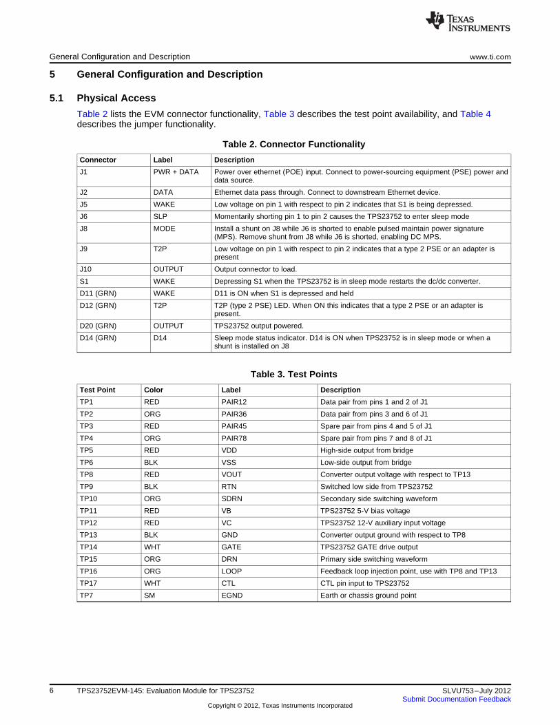
Table 2 lists the EVM connector functionality, Table 3 describes the test point availability, and Table 4describes the jumper functionality.
Table 2. Connector Functionality
Connector Label Description
J1 PWR + DATA Power over ethernet (POE) input. Connect to power-sourcing equipment (PSE) power anddata source.
J2 DATA Ethernet data pass through. Connect to downstream Ethernet device.
J5 WAKE Low voltage on pin 1 with respect to pin 2 indicates that S1 is being depressed.
J6 SLP Momentarily shorting pin 1 to pin 2 causes the TPS23752 to enter sleep mode
J8 MODE Install a shunt on J8 while J6 is shorted to enable pulsed maintain power signature(MPS). Remove shunt from J8 while J6 is shorted, enabling DC MPS.
J9 T2P Low voltage on pin 1 with respect to pin 2 indicates that a type 2 PSE or an adapter ispresent
J10 OUTPUT Output connector to load.
S1 WAKE Depressing S1 when the TPS23752 is in sleep mode restarts the dc/dc converter.
D11 (GRN) WAKE D11 is ON when S1 is depressed and held
D12 (GRN) T2P T2P (type 2 PSE) LED. When ON this indicates that a type 2 PSE or an adapter ispresent.
D20 (GRN) OUTPUT TPS23752 output powered.
D14 (GRN) D14 Sleep mode status indicator. D14 is ON when TPS23752 is in sleep mode or when ashunt is installed on J8
Table 3. Test Points
Test Point Color Label Description
TP1 RED PAIR12 Data pair from pins 1 and 2 of J1
TP2 ORG PAIR36 Data pair from pins 3 and 6 of J1
TP3 RED PAIR45 Spare pair from pins 4 and 5 of J1
TP4 ORG PAIR78 Spare pair from pins 7 and 8 of J1
TP5 RED VDD High-side output from bridge
TP6 BLK VSS Low-side output from bridge
TP8 RED VOUT Converter output voltage with respect to TP13
TP9 BLK RTN Switched low side from TPS23752
TP10 ORG SDRN Secondary side switching waveform
TP11 RED VB TPS23752 5-V bias voltage
TP12 RED VC TPS23752 12-V auxiliary input voltage
TP13 BLK GND Converter output ground with respect to TP8
TP14 WHT GATE TPS23752 GATE drive output
TP15 ORG DRN Primary side switching waveform
TP16 ORG LOOP Feedback loop injection point, use with TP8 and TP13
TP17 WHT CTL CTL pin input to TPS23752
TP7 SM EGND Earth or chassis ground point
6 TPS23752EVM-145: Evaluation Module for TPS23752 SLVU753–July 2012Submit Documentation Feedback
Copyright © 2012, Texas Instruments Incorporated

- +
DUTTPS23752EVM-145
J1
J2
J3
J10
VOUT
GND
PSE
EthernetDevice
(Ethernet Cable)
WallAdapter
+ ±
www.ti.com TPS23752EVM-145 Performance Data
Table 4. Jumpers
Jumper Label Description
J4 J4 D11 LED bias jumper. Installing enables WAKE LED.
J7 J5 D12 LED bias jumper. Installing enables T2P LED. Shunt may be removed whenmaking efficiency measurements.
J11 J11 D20 LED bias jumper. Installing enables OUTPUT LED. Shunt may be removed whenmaking efficiency measurements.
5.2 Test Setup
Figure 3 shows a typical test setup for the EVM. Connect J1 to the power sourcing equipment (PSE)Power for the Ethernet device is available at J10 and the pass-through Ethernet data is available at J2.
Figure 3. Typical TPS23752EVM-145 Test Setup
6 TPS23752EVM-145 Performance Data
6.1 Efficiency
Figure 4, Figure 5, and Figure 6 illustrate the efficiency of the EVM. Figure 4 efficiency is measuredbetween the J1 input interface and J10 output connector while Figure 5 and Figure 6 are measuredbetween TP5/TP6 and J10 to exclude the diode bridge and Ethernet transformer losses. Figure 6demonstrates the light-load efficiency improvement provided by the VFO mode.
7SLVU753–July 2012 TPS23752EVM-145: Evaluation Module for TPS23752Submit Documentation Feedback
Copyright © 2012, Texas Instruments Incorporated

40
45
50
55
60
65
70
75
80
85
90
0 0.2 0.4 0.6 0.8 1
Load Current (A)
Effic
iency (
%)
PWM Mode Only
PWM−>VFO Mode
G003
0
10
20
30
40
50
60
70
80
90
0 1 2 3 4 5
Load Current (A)
Effic
iency (
%)
PWM Mode Only
PWM−>VFO Mode
G002
0
10
20
30
40
50
60
70
80
90
0 1 2 3 4 5
Load Current (A)
Effic
ien
cy (
%)
G001
TPS23752EVM-145 Performance Data www.ti.com
Figure 4. PoE End-End Efficiency
Figure 5. DC/DC Converter Efficiency
Figure 6. DC/DC Converter Light-Load Efficiency
8 TPS23752EVM-145: Evaluation Module for TPS23752 SLVU753–July 2012Submit Documentation Feedback
Copyright © 2012, Texas Instruments Incorporated

www.ti.com EVM Assembly Drawings and Layout Guidelines
7 EVM Assembly Drawings and Layout Guidelines
7.1 PCB Drawings
Figure 7 through Figure 12 show component placement and layout.
Figure 7. Top-Side Placement
Figure 8. Top-Side Routing
9SLVU753–July 2012 TPS23752EVM-145: Evaluation Module for TPS23752Submit Documentation Feedback
Copyright © 2012, Texas Instruments Incorporated

EVM Assembly Drawings and Layout Guidelines www.ti.com
Figure 9. Layer Two Routing
Figure 10. Layer Three Routing
10 TPS23752EVM-145: Evaluation Module for TPS23752 SLVU753–July 2012Submit Documentation Feedback
Copyright © 2012, Texas Instruments Incorporated

www.ti.com EVM Assembly Drawings and Layout Guidelines
Figure 11. Bottom-Side Routing
Figure 12. Bottom-Side Placement
11SLVU753–July 2012 TPS23752EVM-145: Evaluation Module for TPS23752Submit Documentation Feedback
Copyright © 2012, Texas Instruments Incorporated

EVM Assembly Drawings and Layout Guidelines www.ti.com
7.2 Layout Guidelines
Follow power and EMI/ESD best practice guidelines for the layout of the PoE front end. A basic set ofrecommendations include:
• Parts placement must be driven by power flow in a point-to-point manner; RJ-45, Ethernet transformer,diode bridges, TVS and 0.1-μF capacitor, and TPS23752 converter input bulk capacitor.
• Make all leads as short as possible with wide power traces and paired signal and return.
• No crossovers of signals are allowed from one part of the flow to another.
• Observe spacing consistent with safety standards, like IEC60950, between the 48-V input voltage railsand between the input and an isolated-converter output.
• Place the TPS23752 over split, local ground planes referenced to VSS for the PoE input and to RTNfor the converter. Whereas the PoE side may operate without a ground plane, the converter side musthave one. Make sure no logic ground and power layers are present under the Ethernet input or theconverter primary side.
• Use large copper fills and traces on SMT power-dissipating devices, and use wide traces or overlaycopper fills in the power path.
The DC/DC Converter layout benefits from basic rules, such as:
• Pair signals, reducing emissions and noise, especially the paths that carry high-current pulses whichinclude the power semiconductors and magnetics.
• Minimize the trace length of high current, power semiconductors, and magnetic components.
• Use vertical pairing, where possible.
• Use the ground plane for the switching currents carefully.
• Keep the high-current and high-voltage switching away from low-level sensing circuits, including thoseoutside the power supply.
• Maintain proper spacing around the high-voltage sections of the converter.
12 TPS23752EVM-145: Evaluation Module for TPS23752 SLVU753–July 2012Submit Documentation Feedback
Copyright © 2012, Texas Instruments Incorporated

www.ti.com EVM Assembly Drawings and Layout Guidelines
7.3 EMI Containment• Use compact loops for dv/dt and di/dt circuit paths (power loops and gate drives)
• Use minimal, yet thermally adequate, copper areas for heat sinking of components tied to switchingnodes (minimize exposed radiating surface).
• Use copper-ground planes (possible stitching) and top-layer copper floods (surround circuitry withground floods)
• Use 4-layer PCB, if economically feasible (for better grounding)
• Minimize the amount of copper area associated with input traces (minimizing radiated pickup)
• Hide copper associated with switching nodes under shielded magnetics, where possible
• Heat sink the quiet side of components instead of the switching side, where possible (like the outputside of inductor)
• Use Bob Smith terminations, Bob Smith EFT capacitor, and Bob Smith plane
• Use Bob Smith plane as a ground shield on the input side of the PCB (creating a phantom or literalearth ground)
• Use an LC filter at the DC/DC input
• Dampen high frequency ringing on all switching nodes, if present (allow for possible snubbers)
• Control rise times with gate-drive resistors and possibly snubbers
• Switching frequency considerations
• Use an EMI bridge capacitor across isolation boundary (isolated topologies)
• Observe the polarity dot on inductors (embed noisy end)
• Use ferrite beads on input (allow for possible use of beads or 0-Ω resistors)
• Maintain physical separation between input-related circuitry and power circuitry (use ferrite beads asboundary line)
• Balance efficiency vs acceptable noise margin
• Possible use of common-mode inductors
• Possible use of integrated RJ-45 jacks (shielded with internal transformer and Bob Smith terminations)
• End-product enclosure considerations (shielding)
13SLVU753–July 2012 TPS23752EVM-145: Evaluation Module for TPS23752Submit Documentation Feedback
Copyright © 2012, Texas Instruments Incorporated

Bill of Materials www.ti.com
8 Bill of Materials
Table 5. TPS23752EVM-145 Bill of Materials
COUNT REFDES VALUE DESCRIPTION SIZE PART NUMBER SUPPLIER
2 C1, C10 1000 pF Capacitor, ceramic, 2 kV, X7R, 15% 1210 Std STD
2 C12, C30 0.1 µF Capacitor, ceramic, 25 V, X7R, 10% 603 Std Std
5 C13-14, C32-34 0.47 µF Capacitor, ceramic, 16 V, X7R, 10% 603 STD Std
1 C16 47 µF Capacitor, Aluminum, 63 V, ±20% 0.328 × 0.390 in EEE-FK1J470P Panasonic
2 C17-18 1 µF Capacitor, ceramic, 100 V, X7R, 10% 1210 Std STD
3 C20-22 47 µF Capacitor, ceramic, 10 V, X5R, 15% 1210 Std Std
2 C23-24 330 µF Capacitor, aluminum, 6.3 V, 20% 0.260 × 0.276 in EEE-FK0J331XP Panasonic
6 C2-5, C11, C37 0.01 µF Capacitor, ceramic, 100 V, X7R, 10% 603 STD STD
2 C25, C38 1 µF Capacitor, ceramic, 16 V, X7R, 10% 603 STD Std
1 C26 2200 pF Capacitor, ceramic, 2 kV, X7R, 15% 1812 Std Std
1 C27 22 µF Capacitor, Aluminum, 25 V, 20% 5 × 5.8 mm EEE-FK1E220R Panasonic
1 C29 1 µF Capacitor, ceramic, 25 V, X7R, 10% 603 STD Std
1 C31 330 pF Capacitor, ceramic, 50 V, C0G, 10% 603 STD Std
0 C35 0.1 µF Capacitor, ceramic, 50 V, X7R, 10% 603 STD Std
1 C36 0.022 µF Capacitor, ceramic, 50 V, X7R, 10% 603 STD Std
3 C6, C8, C28 1000 pF Capacitor, ceramic, 100 V, X7R, 10% 603 STD STD
4 C7, C9, C15, C19 0.1 µF Capacitor, Ceramic, 100 V, X7R, 10% 805 STD STD
4 D11-12, D14, D20 LN1371G Diode, LED, Green, 10 mA, 2.6 mcd 0.114 × 0.049 in LN1371G Panasonic
1 D13 MURS120T3G Diode, ultra-fast rectifier, 1 A, 200 V SMB MURS120T3G On Semi
1 D15 1N4148W-7-F Diode, signal, 300 mA, 75 V, 350 mW SOD-123 1N4148W-7-F Diodes
9 D1-5, D7-10 B2100-13-F Diode, Schottky, 2 A, 100 V SMB B2100-13-F Diodes
1 D16 MBR0530 Diode, Schottky, 0.5 A, 30 V SOD-123 MBR0530T1G On Semi
1 D17 PDS1040 Diode, Schottky, 10 A, 40 V Power DI 5 PDS1040-13 Diodes, Inc
2 D18-19 BAT54S Diode, Dual Schottky, 200 mA, 30 V SOT323 BAT54SWT1G On Semi
1 D6 SMAJ58A Diode, TVS, 58-V, 1W SMA SMAJ58A-13-F Diodes
4 FB1-4 500 Bead, ferrite, 2000 mA, 60 mΩ 1206 MI1206L501R-10 Steward
2 J1-2 5520252-4 Connector, jack, modular, 8 POS 0.705 × 0.820 inch 5520252-4 AMP
2 J3, J10 ED555/2DS Terminal block, 2 pin, 6 A, 3.5 mm 0.27 × 0.25 inch ED555/2DS OST
7 J4-9, J11 PEC02SAAN Header, male 2 pin, 100 mil spacing 0.100 inch × 2 PEC02SAAN Sullins
1 L1 3.3uH Inductor, SMT, 1.9 A, 80 mΩ 4 × 4 mm LPS4018-332ML Coilcraft
1 L2 0.33uH Inductor, SMT, 19.2 A, 3.52 mΩ 5.3 × 5.5 mm XAL5030-331ME Coilcraft
3 Q1-2, Q7 BSS84 MOSFET, Pch, -50 V, -0.13 A, 10 Ω SOT23 BSS84LT1C Infineon
1 Q3 SiR422DP MOSFET, NChan, 40 V, 40 A, 6.6 mΩ PWRPAK S0-8 SIR422DP-T1-GE3 Vishay
1 Q4 MMBT2907A Trans, PNP, 40 V, 200 mA, 225 mW SOT23 MMBT2907ALT1G On Semi
1 Q5 Si7898DP MOSFET, NChannel, 150 V, 4.8 A, 85 mΩ PWRPAK S0-8 SI7898DP-T1-E3 Vishay
1 Q6 MMBT3906 Trans, PNP, 40 V, 200 mA, 225 mW SOT23 MMBT3906LT1G On Semi
1 Q8 Si2304DDS MOSFET, N-ch, 30 V, 3.6 A, 60 mΩ SOT23 Si2304DDS Vishay
1 Q9 MMBT3904 Trans, NPN, 40 V, 200 mA, 225 mW SOT23 MMBT3904LT1G On Semi
14 TPS23752EVM-145: Evaluation Module for TPS23752 SLVU753–July 2012Submit Documentation Feedback
Copyright © 2012, Texas Instruments Incorporated

www.ti.com Bill of Materials
Table 5. TPS23752EVM-145 Bill of Materials (continued)COUNT REFDES VALUE DESCRIPTION SIZE PART NUMBER SUPPLIER
1 R10 8.87 kΩ Resistor, chip, 1/16W, 1% 603 STD STD
5 R11, R15, R18, 1 kΩ Resistor, chip, 1/16W, 1% 603 STD StdR44, R50
4 R12-14, R19 15 kΩ Resistor, chip, 1/16W, 1% 603 STD Std
8 R1-4, R6-9 75 Ω Resistor, chip, 1/16W, 1% 603 STD STD
2 R16, R20 1.5 kΩ Resistor, chip, 1/16W, 1% 603 STD Std
1 R17 392 kΩ Resistor, chip, 1/16W, 1% 603 STD Std
1 R21 24.9 kΩ Resistor, chip, 1/16W, 1% 603 STD Std
1 R22 39 kΩ Resistor, chip, 1/4W, 5% 1206 Std Std
1 R23 24.9 kΩ Resistor, chip, 1/16W, 1% 603 STD Std
1 R24 750 kΩ Resistor, chip, 1/16W, 1% 603 STD Std
1 R25 10 Ω Resistor, chip, 1/10W, 5% 805 STD STD
1 R26 63.4 Ω Resistor, chip, 1/10W, 1% 805 Std Std
1 R27 6.19 kΩ Resistor, chip, 1/16W, 1% 603 STD Std
1 R28 34 kΩ Resistor, chip, 1/16W, 1% 603 STD Std
4 R29, R33, R37, R48 10 kΩ Resistor, chip, 1/16W, 1% 603 STD Std
1 R30 10 Ω Resistor, chip, 1W, 5% 2512 Std Std
2 R5, R31 100 kΩ Resistor, chip, 1/16W, 1% 603 STD Std
2 R32, R38 43.2 Ω Resistor, chip, 1/16W, 1% 603 STD Std
1 R34 0.09 Ω Resistor, chip, 1/2W, 1% 2010 Std Std
1 R35 16.9 kΩ Resistor, chip, 1/16W, 1% 603 STD Std
1 R36 332 Ω Resistor, chip, 1/16W, 1% 603 STD Std
1 R39 0 Ω Resistor, chip, 1/16W, 1% 603 STD Std
1 R40 20 kΩ Resistor, chip, 1/16W, 1% 603 STD Std
2 R41, R42 30.1 kΩ Resistor, chip, 1/16W, 1% 603 STD Std
1 R43 10 kΩ Resistor, chip, 1/16W, 1% 603 STD Std
1 R45 3.65 kΩ Resistor, chip, 1/16W, 1% 603 STD Std
1 R46 49.9 Ω Resistor, chip, 1/16W, 1% 603 STD Std
1 R47 604 Ω Resistor, chip, 1/16W, 1% 603 STD Std
1 R49 41.2 kΩ Resistor, chip, 1/16W, 1% 603 STD Std
1 R51 13.7 kΩ Resistor, chip, 1/16W, 1% 603 STD Std
1 S1 KT11P2JM34LFS Switch, SPST, PB Momentary, Sealed Washable 0.245 × 0.251 in KT11P2JM34LFS C & K
1 T1 749022011 PoE Plus Gigabit Ethernet Transformer S024 749022011 Wurth Electronics
or or or
H6096NL H6096NL Pulse
1 T2 JA4456-DL Transformer, SMT For PoE/PD, 25 W, 2.8 A 0.810 × 1.181 in JA4456-DL Coilcraft
1 T3 PA0184 XFMR, SMT gate drive 0.355 × 0.340 in PA0184NL Pulse
6 TP1, TP3, TP5, 5010 Test point, red, thru hole 0.125 × 0.125 in 5010 KeystoneTP8, TP11-12
2 TP14, TP17 5012 Test point, white, thru hole 0.125 × 0.125 in 5012 Keystone
15SLVU753–July 2012 TPS23752EVM-145: Evaluation Module for TPS23752Submit Documentation Feedback
Copyright © 2012, Texas Instruments Incorporated

Bill of Materials www.ti.com
Table 5. TPS23752EVM-145 Bill of Materials (continued)COUNT REFDES VALUE DESCRIPTION SIZE PART NUMBER SUPPLIER
5 TP2, TP4, TP10, 5013 Test point, orange, thru hole 0.125 × 0.125 in 5013 KeystoneTP15-16
3 TP6, TP9, TP13 5011 Test point, black, thru hole 0.125 × 0.125 in 5011 Keystone
1 TP7 5016 Test point, SM, 0.150 × 0.090 0.185 × 0.135 in 5016 Keystone
5 U1-4, U6 PC357N4J000F Photocoupler, 300-600% CTR, 3.75 kV isolation MF4 PC357N4J000F Sharp
1 U5 TPS23752PWP IC, IEEE 802.3 AT PoE interface & green mode DC-DC controller HTSSOP TPS23752PWP TI
1 U7 TCMT1107 IC, photocoupler, 3750 VRMS, 80-160% CTR MF4 TCMT1107 Vishay
1 U8 TLV431A IC, shunt regulator, 6 V, 10 mA, 1% SOT23-5 TLV431ACDBVR TI
3 -- Shunt, black 100-mil STC02SYAN Sullins Connector
Solutions
1 -- PCB, 3.5 in × 1.7 in × 0.062 in PWR145 Any
16 TPS23752EVM-145: Evaluation Module for TPS23752 SLVU753–July 2012Submit Documentation Feedback
Copyright © 2012, Texas Instruments Incorporated
EVALUATION BOARD/KIT/MODULE (EVM) ADDITIONAL TERMS
Texas Instruments (TI) provides the enclosed Evaluation Board/Kit/Module (EVM) under the following conditions:
The user assumes all responsibility and liability for proper and safe handling of the goods. Further, the user indemnifies TI from all claimsarising from the handling or use of the goods.
Should this evaluation board/kit not meet the specifications indicated in the User’s Guide, the board/kit may be returned within 30 days fromthe date of delivery for a full refund. THE FOREGOING LIMITED WARRANTY IS THE EXCLUSIVE WARRANTY MADE BY SELLER TOBUYER AND IS IN LIEU OF ALL OTHER WARRANTIES, EXPRESSED, IMPLIED, OR STATUTORY, INCLUDING ANY WARRANTY OFMERCHANTABILITY OR FITNESS FOR ANY PARTICULAR PURPOSE. EXCEPT TO THE EXTENT OF THE INDEMNITY SET FORTHABOVE, NEITHER PARTY SHALL BE LIABLE TO THE OTHER FOR ANY INDIRECT, SPECIAL, INCIDENTAL, OR CONSEQUENTIALDAMAGES.
Please read the User's Guide and, specifically, the Warnings and Restrictions notice in the User's Guide prior to handling the product. Thisnotice contains important safety information about temperatures and voltages. For additional information on TI's environmental and/or safetyprograms, please visit www.ti.com/esh or contact TI.
No license is granted under any patent right or other intellectual property right of TI covering or relating to any machine, process, orcombination in which such TI products or services might be or are used. TI currently deals with a variety of customers for products, andtherefore our arrangement with the user is not exclusive. TI assumes no liability for applications assistance, customer product design,software performance, or infringement of patents or services described herein.
REGULATORY COMPLIANCE INFORMATION
As noted in the EVM User’s Guide and/or EVM itself, this EVM and/or accompanying hardware may or may not be subject to the FederalCommunications Commission (FCC) and Industry Canada (IC) rules.
For EVMs not subject to the above rules, this evaluation board/kit/module is intended for use for ENGINEERING DEVELOPMENT,DEMONSTRATION OR EVALUATION PURPOSES ONLY and is not considered by TI to be a finished end product fit for general consumeruse. It generates, uses, and can radiate radio frequency energy and has not been tested for compliance with the limits of computingdevices pursuant to part 15 of FCC or ICES-003 rules, which are designed to provide reasonable protection against radio frequencyinterference. Operation of the equipment may cause interference with radio communications, in which case the user at his own expense willbe required to take whatever measures may be required to correct this interference.
General Statement for EVMs including a radio
User Power/Frequency Use Obligations: This radio is intended for development/professional use only in legally allocated frequency andpower limits. Any use of radio frequencies and/or power availability of this EVM and its development application(s) must comply with locallaws governing radio spectrum allocation and power limits for this evaluation module. It is the user’s sole responsibility to only operate thisradio in legally acceptable frequency space and within legally mandated power limitations. Any exceptions to this are strictly prohibited andunauthorized by Texas Instruments unless user has obtained appropriate experimental/development licenses from local regulatoryauthorities, which is responsibility of user including its acceptable authorization.
For EVMs annotated as FCC – FEDERAL COMMUNICATIONS COMMISSION Part 15 Compliant
Caution
This device complies with part 15 of the FCC Rules. Operation is subject to the following two conditions: (1) This device may not causeharmful interference, and (2) this device must accept any interference received, including interference that may cause undesired operation.
Changes or modifications not expressly approved by the party responsible for compliance could void the user's authority to operate theequipment.
FCC Interference Statement for Class A EVM devices
This equipment has been tested and found to comply with the limits for a Class A digital device, pursuant to part 15 of the FCC Rules.These limits are designed to provide reasonable protection against harmful interference when the equipment is operated in a commercialenvironment. This equipment generates, uses, and can radiate radio frequency energy and, if not installed and used in accordance with theinstruction manual, may cause harmful interference to radio communications. Operation of this equipment in a residential area is likely tocause harmful interference in which case the user will be required to correct the interference at his own expense.

FCC Interference Statement for Class B EVM devices
This equipment has been tested and found to comply with the limits for a Class B digital device, pursuant to part 15 of the FCC Rules.These limits are designed to provide reasonable protection against harmful interference in a residential installation. This equipmentgenerates, uses and can radiate radio frequency energy and, if not installed and used in accordance with the instructions, may causeharmful interference to radio communications. However, there is no guarantee that interference will not occur in a particular installation. Ifthis equipment does cause harmful interference to radio or television reception, which can be determined by turning the equipment off andon, the user is encouraged to try to correct the interference by one or more of the following measures:
• Reorient or relocate the receiving antenna.• Increase the separation between the equipment and receiver.• Connect the equipment into an outlet on a circuit different from that to which the receiver is connected.• Consult the dealer or an experienced radio/TV technician for help.
For EVMs annotated as IC – INDUSTRY CANADA Compliant
This Class A or B digital apparatus complies with Canadian ICES-003.
Changes or modifications not expressly approved by the party responsible for compliance could void the user’s authority to operate theequipment.
Concerning EVMs including radio transmitters
This device complies with Industry Canada licence-exempt RSS standard(s). Operation is subject to the following two conditions: (1) thisdevice may not cause interference, and (2) this device must accept any interference, including interference that may cause undesiredoperation of the device.
Concerning EVMs including detachable antennas
Under Industry Canada regulations, this radio transmitter may only operate using an antenna of a type and maximum (or lesser) gainapproved for the transmitter by Industry Canada. To reduce potential radio interference to other users, the antenna type and its gain shouldbe so chosen that the equivalent isotropically radiated power (e.i.r.p.) is not more than that necessary for successful communication.
This radio transmitter has been approved by Industry Canada to operate with the antenna types listed in the user guide with the maximumpermissible gain and required antenna impedance for each antenna type indicated. Antenna types not included in this list, having a gaingreater than the maximum gain indicated for that type, are strictly prohibited for use with this device.
Cet appareil numérique de la classe A ou B est conforme à la norme NMB-003 du Canada.
Les changements ou les modifications pas expressément approuvés par la partie responsable de la conformité ont pu vider l’autorité del'utilisateur pour actionner l'équipement.
Concernant les EVMs avec appareils radio
Le présent appareil est conforme aux CNR d'Industrie Canada applicables aux appareils radio exempts de licence. L'exploitation estautorisée aux deux conditions suivantes : (1) l'appareil ne doit pas produire de brouillage, et (2) l'utilisateur de l'appareil doit accepter toutbrouillage radioélectrique subi, même si le brouillage est susceptible d'en compromettre le fonctionnement.
Concernant les EVMs avec antennes détachables
Conformément à la réglementation d'Industrie Canada, le présent émetteur radio peut fonctionner avec une antenne d'un type et d'un gainmaximal (ou inférieur) approuvé pour l'émetteur par Industrie Canada. Dans le but de réduire les risques de brouillage radioélectrique àl'intention des autres utilisateurs, il faut choisir le type d'antenne et son gain de sorte que la puissance isotrope rayonnée équivalente(p.i.r.e.) ne dépasse pas l'intensité nécessaire à l'établissement d'une communication satisfaisante.
Le présent émetteur radio a été approuvé par Industrie Canada pour fonctionner avec les types d'antenne énumérés dans le manueld’usage et ayant un gain admissible maximal et l'impédance requise pour chaque type d'antenne. Les types d'antenne non inclus danscette liste, ou dont le gain est supérieur au gain maximal indiqué, sont strictement interdits pour l'exploitation de l'émetteur.
SPACER
SPACER
SPACER
SPACER
SPACER
SPACER
SPACER
SPACER

【【Important Notice for Users of this Product in Japan】】This development kit is NOT certified as Confirming to Technical Regulations of Radio Law of Japan
If you use this product in Japan, you are required by Radio Law of Japan to follow the instructions below with respect to this product:
1. Use this product in a shielded room or any other test facility as defined in the notification #173 issued by Ministry of Internal Affairs andCommunications on March 28, 2006, based on Sub-section 1.1 of Article 6 of the Ministry’s Rule for Enforcement of Radio Law ofJapan,
2. Use this product only after you obtained the license of Test Radio Station as provided in Radio Law of Japan with respect to thisproduct, or
3. Use of this product only after you obtained the Technical Regulations Conformity Certification as provided in Radio Law of Japan withrespect to this product. Also, please do not transfer this product, unless you give the same notice above to the transferee. Please notethat if you could not follow the instructions above, you will be subject to penalties of Radio Law of Japan.
Texas Instruments Japan Limited(address) 24-1, Nishi-Shinjuku 6 chome, Shinjuku-ku, Tokyo, Japan
http://www.tij.co.jp
【ご使用にあたっての注】
本開発キットは技術基準適合証明を受けておりません。
本製品のご使用に際しては、電波法遵守のため、以下のいずれかの措置を取っていただく必要がありますのでご注意ください。1. 電波法施行規則第6条第1項第1号に基づく平成18年3月28日総務省告示第173号で定められた電波暗室等の試験設備でご使用いただく。2. 実験局の免許を取得後ご使用いただく。3. 技術基準適合証明を取得後ご使用いただく。
なお、本製品は、上記の「ご使用にあたっての注意」を譲渡先、移転先に通知しない限り、譲渡、移転できないものとします。
上記を遵守頂けない場合は、電波法の罰則が適用される可能性があることをご留意ください。
日本テキサス・インスツルメンツ株式会社東京都新宿区西新宿6丁目24番1号西新宿三井ビルhttp://www.tij.co.jp
SPACER
SPACER
SPACER
SPACER
SPACER
SPACER
SPACER
SPACER
SPACER
SPACER
SPACER
SPACER
SPACER
SPACER
SPACER
SPACER

EVALUATION BOARD/KIT/MODULE (EVM)WARNINGS, RESTRICTIONS AND DISCLAIMERS
For Feasibility Evaluation Only, in Laboratory/Development Environments. Unless otherwise indicated, this EVM is not a finishedelectrical equipment and not intended for consumer use. It is intended solely for use for preliminary feasibility evaluation inlaboratory/development environments by technically qualified electronics experts who are familiar with the dangers and application risksassociated with handling electrical mechanical components, systems and subsystems. It should not be used as all or part of a finished endproduct.
Your Sole Responsibility and Risk. You acknowledge, represent and agree that:
1. You have unique knowledge concerning Federal, State and local regulatory requirements (including but not limited to Food and DrugAdministration regulations, if applicable) which relate to your products and which relate to your use (and/or that of your employees,affiliates, contractors or designees) of the EVM for evaluation, testing and other purposes.
2. You have full and exclusive responsibility to assure the safety and compliance of your products with all such laws and other applicableregulatory requirements, and also to assure the safety of any activities to be conducted by you and/or your employees, affiliates,contractors or designees, using the EVM. Further, you are responsible to assure that any interfaces (electronic and/or mechanical)between the EVM and any human body are designed with suitable isolation and means to safely limit accessible leakage currents tominimize the risk of electrical shock hazard.
3. You will employ reasonable safeguards to ensure that your use of the EVM will not result in any property damage, injury or death, evenif the EVM should fail to perform as described or expected.
4. You will take care of proper disposal and recycling of the EVM’s electronic components and packing materials.
Certain Instructions. It is important to operate this EVM within TI’s recommended specifications and environmental considerations per theuser guidelines. Exceeding the specified EVM ratings (including but not limited to input and output voltage, current, power, andenvironmental ranges) may cause property damage, personal injury or death. If there are questions concerning these ratings please contacta TI field representative prior to connecting interface electronics including input power and intended loads. Any loads applied outside of thespecified output range may result in unintended and/or inaccurate operation and/or possible permanent damage to the EVM and/orinterface electronics. Please consult the EVM User's Guide prior to connecting any load to the EVM output. If there is uncertainty as to theload specification, please contact a TI field representative. During normal operation, some circuit components may have case temperaturesgreater than 60°C as long as the input and output are maintained at a normal ambient operating temperature. These components includebut are not limited to linear regulators, switching transistors, pass transistors, and current sense resistors which can be identified using theEVM schematic located in the EVM User's Guide. When placing measurement probes near these devices during normal operation, pleasebe aware that these devices may be very warm to the touch. As with all electronic evaluation tools, only qualified personnel knowledgeablein electronic measurement and diagnostics normally found in development environments should use these EVMs.
Agreement to Defend, Indemnify and Hold Harmless. You agree to defend, indemnify and hold TI, its licensors and their representativesharmless from and against any and all claims, damages, losses, expenses, costs and liabilities (collectively, "Claims") arising out of or inconnection with any use of the EVM that is not in accordance with the terms of the agreement. This obligation shall apply whether Claimsarise under law of tort or contract or any other legal theory, and even if the EVM fails to perform as described or expected.
Safety-Critical or Life-Critical Applications. If you intend to evaluate the components for possible use in safety critical applications (suchas life support) where a failure of the TI product would reasonably be expected to cause severe personal injury or death, such as deviceswhich are classified as FDA Class III or similar classification, then you must specifically notify TI of such intent and enter into a separateAssurance and Indemnity Agreement.
Mailing Address: Texas Instruments, Post Office Box 655303, Dallas, Texas 75265Copyright © 2012, Texas Instruments Incorporated

EVALUATION BOARD/KIT/MODULE (EVM) ADDITIONAL TERMSTexas Instruments (TI) provides the enclosed Evaluation Board/Kit/Module (EVM) under the following conditions:
The user assumes all responsibility and liability for proper and safe handling of the goods. Further, the user indemnifies TI from all claimsarising from the handling or use of the goods.
Should this evaluation board/kit not meet the specifications indicated in the User’s Guide, the board/kit may be returned within 30 days fromthe date of delivery for a full refund. THE FOREGOING LIMITED WARRANTY IS THE EXCLUSIVE WARRANTY MADE BY SELLER TOBUYER AND IS IN LIEU OF ALL OTHER WARRANTIES, EXPRESSED, IMPLIED, OR STATUTORY, INCLUDING ANY WARRANTY OFMERCHANTABILITY OR FITNESS FOR ANY PARTICULAR PURPOSE. EXCEPT TO THE EXTENT OF THE INDEMNITY SET FORTHABOVE, NEITHER PARTY SHALL BE LIABLE TO THE OTHER FOR ANY INDIRECT, SPECIAL, INCIDENTAL, OR CONSEQUENTIALDAMAGES.
Please read the User's Guide and, specifically, the Warnings and Restrictions notice in the User's Guide prior to handling the product. Thisnotice contains important safety information about temperatures and voltages. For additional information on TI's environmental and/or safetyprograms, please visit www.ti.com/esh or contact TI.
No license is granted under any patent right or other intellectual property right of TI covering or relating to any machine, process, orcombination in which such TI products or services might be or are used. TI currently deals with a variety of customers for products, andtherefore our arrangement with the user is not exclusive. TI assumes no liability for applications assistance, customer product design,software performance, or infringement of patents or services described herein.
REGULATORY COMPLIANCE INFORMATIONAs noted in the EVM User’s Guide and/or EVM itself, this EVM and/or accompanying hardware may or may not be subject to the FederalCommunications Commission (FCC) and Industry Canada (IC) rules.
For EVMs not subject to the above rules, this evaluation board/kit/module is intended for use for ENGINEERING DEVELOPMENT,DEMONSTRATION OR EVALUATION PURPOSES ONLY and is not considered by TI to be a finished end product fit for general consumeruse. It generates, uses, and can radiate radio frequency energy and has not been tested for compliance with the limits of computingdevices pursuant to part 15 of FCC or ICES-003 rules, which are designed to provide reasonable protection against radio frequencyinterference. Operation of the equipment may cause interference with radio communications, in which case the user at his own expense willbe required to take whatever measures may be required to correct this interference.
General Statement for EVMs including a radioUser Power/Frequency Use Obligations: This radio is intended for development/professional use only in legally allocated frequency andpower limits. Any use of radio frequencies and/or power availability of this EVM and its development application(s) must comply with locallaws governing radio spectrum allocation and power limits for this evaluation module. It is the user’s sole responsibility to only operate thisradio in legally acceptable frequency space and within legally mandated power limitations. Any exceptions to this are strictly prohibited andunauthorized by Texas Instruments unless user has obtained appropriate experimental/development licenses from local regulatoryauthorities, which is responsibility of user including its acceptable authorization.
For EVMs annotated as FCC – FEDERAL COMMUNICATIONS COMMISSION Part 15 Compliant
CautionThis device complies with part 15 of the FCC Rules. Operation is subject to the following two conditions: (1) This device may not causeharmful interference, and (2) this device must accept any interference received, including interference that may cause undesired operation.
Changes or modifications not expressly approved by the party responsible for compliance could void the user's authority to operate theequipment.
FCC Interference Statement for Class A EVM devicesThis equipment has been tested and found to comply with the limits for a Class A digital device, pursuant to part 15 of the FCC Rules.These limits are designed to provide reasonable protection against harmful interference when the equipment is operated in a commercialenvironment. This equipment generates, uses, and can radiate radio frequency energy and, if not installed and used in accordance with theinstruction manual, may cause harmful interference to radio communications. Operation of this equipment in a residential area is likely tocause harmful interference in which case the user will be required to correct the interference at his own expense.

FCC Interference Statement for Class B EVM devicesThis equipment has been tested and found to comply with the limits for a Class B digital device, pursuant to part 15 of the FCC Rules.These limits are designed to provide reasonable protection against harmful interference in a residential installation. This equipmentgenerates, uses and can radiate radio frequency energy and, if not installed and used in accordance with the instructions, may causeharmful interference to radio communications. However, there is no guarantee that interference will not occur in a particular installation. Ifthis equipment does cause harmful interference to radio or television reception, which can be determined by turning the equipment off andon, the user is encouraged to try to correct the interference by one or more of the following measures:
• Reorient or relocate the receiving antenna.• Increase the separation between the equipment and receiver.• Connect the equipment into an outlet on a circuit different from that to which the receiver is connected.• Consult the dealer or an experienced radio/TV technician for help.
For EVMs annotated as IC – INDUSTRY CANADA Compliant
This Class A or B digital apparatus complies with Canadian ICES-003.
Changes or modifications not expressly approved by the party responsible for compliance could void the user’s authority to operate theequipment.
Concerning EVMs including radio transmitters
This device complies with Industry Canada licence-exempt RSS standard(s). Operation is subject to the following two conditions: (1) thisdevice may not cause interference, and (2) this device must accept any interference, including interference that may cause undesiredoperation of the device.
Concerning EVMs including detachable antennasUnder Industry Canada regulations, this radio transmitter may only operate using an antenna of a type and maximum (or lesser) gainapproved for the transmitter by Industry Canada. To reduce potential radio interference to other users, the antenna type and its gain shouldbe so chosen that the equivalent isotropically radiated power (e.i.r.p.) is not more than that necessary for successful communication.
This radio transmitter has been approved by Industry Canada to operate with the antenna types listed in the user guide with the maximumpermissible gain and required antenna impedance for each antenna type indicated. Antenna types not included in this list, having a gaingreater than the maximum gain indicated for that type, are strictly prohibited for use with this device.
Cet appareil numérique de la classe A ou B est conforme à la norme NMB-003 du Canada.
Les changements ou les modifications pas expressément approuvés par la partie responsable de la conformité ont pu vider l’autorité del'utilisateur pour actionner l'équipement.
Concernant les EVMs avec appareils radio
Le présent appareil est conforme aux CNR d'Industrie Canada applicables aux appareils radio exempts de licence. L'exploitation estautorisée aux deux conditions suivantes : (1) l'appareil ne doit pas produire de brouillage, et (2) l'utilisateur de l'appareil doit accepter toutbrouillage radioélectrique subi, même si le brouillage est susceptible d'en compromettre le fonctionnement.
Concernant les EVMs avec antennes détachables
Conformément à la réglementation d'Industrie Canada, le présent émetteur radio peut fonctionner avec une antenne d'un type et d'un gainmaximal (ou inférieur) approuvé pour l'émetteur par Industrie Canada. Dans le but de réduire les risques de brouillage radioélectrique àl'intention des autres utilisateurs, il faut choisir le type d'antenne et son gain de sorte que la puissance isotrope rayonnée équivalente(p.i.r.e.) ne dépasse pas l'intensité nécessaire à l'établissement d'une communication satisfaisante.
Le présent émetteur radio a été approuvé par Industrie Canada pour fonctionner avec les types d'antenne énumérés dans le manueld’usage et ayant un gain admissible maximal et l'impédance requise pour chaque type d'antenne. Les types d'antenne non inclus danscette liste, ou dont le gain est supérieur au gain maximal indiqué, sont strictement interdits pour l'exploitation de l'émetteur.
SPACER
SPACER
SPACER
SPACER
SPACER
SPACER
SPACER
SPACER

【【Important Notice for Users of this Product in Japan】】This development kit is NOT certified as Confirming to Technical Regulations of Radio Law of Japan
If you use this product in Japan, you are required by Radio Law of Japan to follow the instructions below with respect to this product:
1. Use this product in a shielded room or any other test facility as defined in the notification #173 issued by Ministry of Internal Affairs andCommunications on March 28, 2006, based on Sub-section 1.1 of Article 6 of the Ministry’s Rule for Enforcement of Radio Law ofJapan,
2. Use this product only after you obtained the license of Test Radio Station as provided in Radio Law of Japan with respect to thisproduct, or
3. Use of this product only after you obtained the Technical Regulations Conformity Certification as provided in Radio Law of Japan withrespect to this product. Also, please do not transfer this product, unless you give the same notice above to the transferee. Please notethat if you could not follow the instructions above, you will be subject to penalties of Radio Law of Japan.
Texas Instruments Japan Limited(address) 24-1, Nishi-Shinjuku 6 chome, Shinjuku-ku, Tokyo, Japan
http://www.tij.co.jp
【ご使用にあたっての注】
本開発キットは技術基準適合証明を受けておりません。
本製品のご使用に際しては、電波法遵守のため、以下のいずれかの措置を取っていただく必要がありますのでご注意ください。1. 電波法施行規則第6条第1項第1号に基づく平成18年3月28日総務省告示第173号で定められた電波暗室等の試験設備でご使用いただく。2. 実験局の免許を取得後ご使用いただく。3. 技術基準適合証明を取得後ご使用いただく。
なお、本製品は、上記の「ご使用にあたっての注意」を譲渡先、移転先に通知しない限り、譲渡、移転できないものとします。
上記を遵守頂けない場合は、電波法の罰則が適用される可能性があることをご留意ください。
日本テキサス・インスツルメンツ株式会社東京都新宿区西新宿6丁目24番1号西新宿三井ビルhttp://www.tij.co.jp
SPACER
SPACER
SPACER
SPACER
SPACER
SPACER
SPACER
SPACER
SPACER
SPACER
SPACER
SPACER
SPACER
SPACER
SPACER
SPACER

EVALUATION BOARD/KIT/MODULE (EVM)WARNINGS, RESTRICTIONS AND DISCLAIMERS
For Feasibility Evaluation Only, in Laboratory/Development Environments. Unless otherwise indicated, this EVM is not a finishedelectrical equipment and not intended for consumer use. It is intended solely for use for preliminary feasibility evaluation inlaboratory/development environments by technically qualified electronics experts who are familiar with the dangers and application risksassociated with handling electrical mechanical components, systems and subsystems. It should not be used as all or part of a finished endproduct.
Your Sole Responsibility and Risk. You acknowledge, represent and agree that:
1. You have unique knowledge concerning Federal, State and local regulatory requirements (including but not limited to Food and DrugAdministration regulations, if applicable) which relate to your products and which relate to your use (and/or that of your employees,affiliates, contractors or designees) of the EVM for evaluation, testing and other purposes.
2. You have full and exclusive responsibility to assure the safety and compliance of your products with all such laws and other applicableregulatory requirements, and also to assure the safety of any activities to be conducted by you and/or your employees, affiliates,contractors or designees, using the EVM. Further, you are responsible to assure that any interfaces (electronic and/or mechanical)between the EVM and any human body are designed with suitable isolation and means to safely limit accessible leakage currents tominimize the risk of electrical shock hazard.
3. You will employ reasonable safeguards to ensure that your use of the EVM will not result in any property damage, injury or death, evenif the EVM should fail to perform as described or expected.
4. You will take care of proper disposal and recycling of the EVM’s electronic components and packing materials.
Certain Instructions. It is important to operate this EVM within TI’s recommended specifications and environmental considerations per theuser guidelines. Exceeding the specified EVM ratings (including but not limited to input and output voltage, current, power, andenvironmental ranges) may cause property damage, personal injury or death. If there are questions concerning these ratings please contacta TI field representative prior to connecting interface electronics including input power and intended loads. Any loads applied outside of thespecified output range may result in unintended and/or inaccurate operation and/or possible permanent damage to the EVM and/orinterface electronics. Please consult the EVM User's Guide prior to connecting any load to the EVM output. If there is uncertainty as to theload specification, please contact a TI field representative. During normal operation, some circuit components may have case temperaturesgreater than 60°C as long as the input and output are maintained at a normal ambient operating temperature. These components includebut are not limited to linear regulators, switching transistors, pass transistors, and current sense resistors which can be identified using theEVM schematic located in the EVM User's Guide. When placing measurement probes near these devices during normal operation, pleasebe aware that these devices may be very warm to the touch. As with all electronic evaluation tools, only qualified personnel knowledgeablein electronic measurement and diagnostics normally found in development environments should use these EVMs.
Agreement to Defend, Indemnify and Hold Harmless. You agree to defend, indemnify and hold TI, its licensors and their representativesharmless from and against any and all claims, damages, losses, expenses, costs and liabilities (collectively, "Claims") arising out of or inconnection with any use of the EVM that is not in accordance with the terms of the agreement. This obligation shall apply whether Claimsarise under law of tort or contract or any other legal theory, and even if the EVM fails to perform as described or expected.
Safety-Critical or Life-Critical Applications. If you intend to evaluate the components for possible use in safety critical applications (suchas life support) where a failure of the TI product would reasonably be expected to cause severe personal injury or death, such as deviceswhich are classified as FDA Class III or similar classification, then you must specifically notify TI of such intent and enter into a separateAssurance and Indemnity Agreement.
Mailing Address: Texas Instruments, Post Office Box 655303, Dallas, Texas 75265Copyright © 2012, Texas Instruments Incorporated

IMPORTANT NOTICE
Texas Instruments Incorporated and its subsidiaries (TI) reserve the right to make corrections, enhancements, improvements and otherchanges to its semiconductor products and services per JESD46, latest issue, and to discontinue any product or service per JESD48, latestissue. Buyers should obtain the latest relevant information before placing orders and should verify that such information is current andcomplete. All semiconductor products (also referred to herein as “components”) are sold subject to TI’s terms and conditions of salesupplied at the time of order acknowledgment.
TI warrants performance of its components to the specifications applicable at the time of sale, in accordance with the warranty in TI’s termsand conditions of sale of semiconductor products. Testing and other quality control techniques are used to the extent TI deems necessaryto support this warranty. Except where mandated by applicable law, testing of all parameters of each component is not necessarilyperformed.
TI assumes no liability for applications assistance or the design of Buyers’ products. Buyers are responsible for their products andapplications using TI components. To minimize the risks associated with Buyers’ products and applications, Buyers should provideadequate design and operating safeguards.
TI does not warrant or represent that any license, either express or implied, is granted under any patent right, copyright, mask work right, orother intellectual property right relating to any combination, machine, or process in which TI components or services are used. Informationpublished by TI regarding third-party products or services does not constitute a license to use such products or services or a warranty orendorsement thereof. Use of such information may require a license from a third party under the patents or other intellectual property of thethird party, or a license from TI under the patents or other intellectual property of TI.
Reproduction of significant portions of TI information in TI data books or data sheets is permissible only if reproduction is without alterationand is accompanied by all associated warranties, conditions, limitations, and notices. TI is not responsible or liable for such altereddocumentation. Information of third parties may be subject to additional restrictions.
Resale of TI components or services with statements different from or beyond the parameters stated by TI for that component or servicevoids all express and any implied warranties for the associated TI component or service and is an unfair and deceptive business practice.TI is not responsible or liable for any such statements.
Buyer acknowledges and agrees that it is solely responsible for compliance with all legal, regulatory and safety-related requirementsconcerning its products, and any use of TI components in its applications, notwithstanding any applications-related information or supportthat may be provided by TI. Buyer represents and agrees that it has all the necessary expertise to create and implement safeguards whichanticipate dangerous consequences of failures, monitor failures and their consequences, lessen the likelihood of failures that might causeharm and take appropriate remedial actions. Buyer will fully indemnify TI and its representatives against any damages arising out of the useof any TI components in safety-critical applications.
In some cases, TI components may be promoted specifically to facilitate safety-related applications. With such components, TI’s goal is tohelp enable customers to design and create their own end-product solutions that meet applicable functional safety standards andrequirements. Nonetheless, such components are subject to these terms.
No TI components are authorized for use in FDA Class III (or similar life-critical medical equipment) unless authorized officers of the partieshave executed a special agreement specifically governing such use.
Only those TI components which TI has specifically designated as military grade or “enhanced plastic” are designed and intended for use inmilitary/aerospace applications or environments. Buyer acknowledges and agrees that any military or aerospace use of TI componentswhich have not been so designated is solely at the Buyer's risk, and that Buyer is solely responsible for compliance with all legal andregulatory requirements in connection with such use.
TI has specifically designated certain components which meet ISO/TS16949 requirements, mainly for automotive use. Components whichhave not been so designated are neither designed nor intended for automotive use; and TI will not be responsible for any failure of suchcomponents to meet such requirements.
Products Applications
Audio www.ti.com/audio Automotive and Transportation www.ti.com/automotive
Amplifiers amplifier.ti.com Communications and Telecom www.ti.com/communications
Data Converters dataconverter.ti.com Computers and Peripherals www.ti.com/computers
DLP® Products www.dlp.com Consumer Electronics www.ti.com/consumer-apps
DSP dsp.ti.com Energy and Lighting www.ti.com/energy
Clocks and Timers www.ti.com/clocks Industrial www.ti.com/industrial
Interface interface.ti.com Medical www.ti.com/medical
Logic logic.ti.com Security www.ti.com/security
Power Mgmt power.ti.com Space, Avionics and Defense www.ti.com/space-avionics-defense
Microcontrollers microcontroller.ti.com Video and Imaging www.ti.com/video
RFID www.ti-rfid.com
OMAP Applications Processors www.ti.com/omap TI E2E Community e2e.ti.com
Wireless Connectivity www.ti.com/wirelessconnectivity
Mailing Address: Texas Instruments, Post Office Box 655303, Dallas, Texas 75265Copyright © 2012, Texas Instruments Incorporated