TPIC7218-Q1 Power Controller and Sensor ASIC for … · Product Folder Sample & Buy Technical...
65
Product Folder Sample & Buy Technical Documents Tools & Software Support & Community TPIC7218-Q1 SLDS182A – AUGUST 2010 – REVISED JULY 2015 TPIC7218-Q1 Power Controller and Sensor ASIC For Braking Applications 1 Device Overview 1.1 Features 1 • Qualified for Automotive Applications • Wheel-Speed Sensor Interface • AEC-Q100 Qualified with the Following Results: – Compatible with Intelligent and Active Wheel- Speed Sensors – Device Temperature Grade 1: –40°C to 125°C Ambient Operating Temperature Range – 4 High-Side Switches With Short-Circuit Protection – Device HBM ESD Classification Level 2 – 4 Low-Side Switches With Short-Circuit – Device CDM ESD Classification Level C4 Protection • PWM Low-Side Drivers – 2 High Voltage Low-Side Output Drivers – 4 PWM Low-Side Driver Outputs – 4 Digital Outputs to Indicate the Speed – Current Limitation – Integrated Data Decoder for Intelligent Wheel- – Thermal Protection: T J = 185°C (Minimum) Speed Sensors – Open-Load Detection • Open-Drain Warning Lamp Drivers – Energy Capability: 30 mJ at T J = 150°C – 2 High Voltage Drivers – Clamp Voltage: 40 V – Thermal Protection With Hysteresis – Low R DSon : 0.3 Ω (Maximum) at T J = 150°C – Current Limitation • Digital Low-Side Drivers –T J = 185°C (Minimum) – 4 Digital Low-Side Driver Outputs –R DSon :4 Ω at T J = 150°C – Current Limitation – Clamp Voltage: 40 V – Thermal Protection: T J = 185°C (Minimum) • Other Features – Open-Load Detection – K-LINE Transceiver – Energy Capability: 50 mJ at T J = 150°C – 3.3-V or 5-V Compatible Digital IO – Clamp Voltage: 40 V – Internal 3.3-V Regulator – Low R DSon : 0.2 Ω (Maximum) at T J = 150°C – Internal Charge Pump • Dual High-Side Power Drivers – 1 Low-Voltage Open-Drain Warning Lamp – Direct Input Control Driver – PWM Capability – Full Duplex SPI Interface – Load Dump (overvoltage) Detection – Watchdog Input With Open-Drain Fault – Programmable overcurrent detection Reporting for Safety – Load Leakage Detection – Pb-Free ASIC – Programmable short-circuit Protection – Compliant With CISPR 25 NB Class 5 for – Fault detection over SPI Conducted and Radiated Emissions 1.2 Applications • Anti-lock Braking Systems (ABS) • Electronic Stability Control Systems (ESC) 1.3 Description The TPIC7218-Q1 device integrates in single package several functions needed in ABS and ESC electronic control units (ECU). This integration coupled with the minimization of the external components saves valuable ECU board space. The TPIC7218-Q1 device is an antilock braking controller capable of directly driving eight solenoid valves with internal high-current low-side drivers. Low-side drivers configured for digital control do not require external voltage clamps. The TPIC7218-Q1 device has gate drive capability for two high-side N-Channel MOSFETs that can be used to drive a pump motor and power to all solenoids. The TPIC7218-Q1 device provides a fault-tolerant interface for both Intelligent and Active wheel-speed sensors to an external microprocessor. The TPIC7218-Q1 device can be used with either 3.3- or 5-V microprocessors and uses a standard SPI (Serial-Peripheral Interface). 1 An IMPORTANT NOTICE at the end of this data sheet addresses availability, warranty, changes, use in safety-critical applications, intellectual property matters and other important disclaimers. PRODUCTION DATA.
Transcript of TPIC7218-Q1 Power Controller and Sensor ASIC for … · Product Folder Sample & Buy Technical...

Product
Folder
Sample &Buy
Technical
Documents
Tools &
Software
Support &Community
TPIC7218-Q1SLDS182A –AUGUST 2010–REVISED JULY 2015
TPIC7218-Q1 Power Controller and Sensor ASIC For Braking Applications1 Device Overview
1.1 Features1
• Qualified for Automotive Applications • Wheel-Speed Sensor Interface• AEC-Q100 Qualified with the Following Results: – Compatible with Intelligent and Active Wheel-
Speed Sensors– Device Temperature Grade 1: –40°C to 125°CAmbient Operating Temperature Range – 4 High-Side Switches With Short-Circuit
Protection– Device HBM ESD Classification Level 2– 4 Low-Side Switches With Short-Circuit– Device CDM ESD Classification Level C4
Protection• PWM Low-Side Drivers– 2 High Voltage Low-Side Output Drivers– 4 PWM Low-Side Driver Outputs– 4 Digital Outputs to Indicate the Speed– Current Limitation– Integrated Data Decoder for Intelligent Wheel-– Thermal Protection: TJ = 185°C (Minimum)
Speed Sensors– Open-Load Detection• Open-Drain Warning Lamp Drivers– Energy Capability: 30 mJ at TJ = 150°C
– 2 High Voltage Drivers– Clamp Voltage: 40 V– Thermal Protection With Hysteresis– Low RDSon: 0.3 Ω (Maximum) at TJ = 150°C– Current Limitation• Digital Low-Side Drivers– TJ = 185°C (Minimum)– 4 Digital Low-Side Driver Outputs– RDSon: 4 Ω at TJ = 150°C– Current Limitation– Clamp Voltage: 40 V– Thermal Protection: TJ = 185°C (Minimum)
• Other Features– Open-Load Detection– K-LINE Transceiver– Energy Capability: 50 mJ at TJ = 150°C– 3.3-V or 5-V Compatible Digital IO– Clamp Voltage: 40 V– Internal 3.3-V Regulator– Low RDSon: 0.2 Ω (Maximum) at TJ = 150°C– Internal Charge Pump• Dual High-Side Power Drivers– 1 Low-Voltage Open-Drain Warning Lamp– Direct Input Control Driver
– PWM Capability – Full Duplex SPI Interface– Load Dump (overvoltage) Detection – Watchdog Input With Open-Drain Fault– Programmable overcurrent detection Reporting for Safety– Load Leakage Detection – Pb-Free ASIC– Programmable short-circuit Protection – Compliant With CISPR 25 NB Class 5 for– Fault detection over SPI Conducted and Radiated Emissions
1.2 Applications• Anti-lock Braking Systems (ABS) • Electronic Stability Control Systems (ESC)
1.3 DescriptionThe TPIC7218-Q1 device integrates in single package several functions needed in ABS and ESCelectronic control units (ECU). This integration coupled with the minimization of the external componentssaves valuable ECU board space.
The TPIC7218-Q1 device is an antilock braking controller capable of directly driving eight solenoid valveswith internal high-current low-side drivers. Low-side drivers configured for digital control do not requireexternal voltage clamps. The TPIC7218-Q1 device has gate drive capability for two high-side N-ChannelMOSFETs that can be used to drive a pump motor and power to all solenoids. The TPIC7218-Q1 deviceprovides a fault-tolerant interface for both Intelligent and Active wheel-speed sensors to an externalmicroprocessor. The TPIC7218-Q1 device can be used with either 3.3- or 5-V microprocessors and usesa standard SPI (Serial-Peripheral Interface).
1
An IMPORTANT NOTICE at the end of this data sheet addresses availability, warranty, changes, use in safety-critical applications,intellectual property matters and other important disclaimers. PRODUCTION DATA.

TPIC7218-Q1SLDS182A –AUGUST 2010–REVISED JULY 2015 www.ti.com
The TPIC7218-Q1 device has two internal open-drain warning lamp drivers that can be pulled up tobattery voltage, as well as one low-voltage driver. An internal state machine monitors a watchdog inputand reports faults on a warning-lamp pin and SPI register. A K-Line transceiver is also included. Amultitude of safety and fault monitoring functionality supervise both system and TPIC7218-Q1 circuits.Faults must be polled and reset over SPI. The TPIC7218-Q1 device is designed for use in harshautomotive environments, capable of withstanding high operating temperatures and electrically noisysignals and power. Short-to-ground, short-to-battery, and open-load conditions are tolerated andmonitored. The TPIC7218-Q1 device also exhibits outstanding Electro-Magnetic Compatibility (EMC)performance.
Device Information (1)
PART NUMBER PACKAGE BODY SIZE (NOM)TPIC7218-Q1 HTQFP (80) 12.00 mm × 12.00 mm
(1) For all available packages, see the orderable addendum at the end of the data sheet.
2 Device Overview Copyright © 2010–2015, Texas Instruments IncorporatedSubmit Documentation Feedback
Product Folder Links: TPIC7218-Q1

TPIC7218-Q1www.ti.com SLDS182A –AUGUST 2010–REVISED JULY 2015
1.4 Functional Block Diagram
Figure 1-1. Functional Block Diagram
Copyright © 2010–2015, Texas Instruments Incorporated Device Overview 3Submit Documentation Feedback
Product Folder Links: TPIC7218-Q1

TPIC7218-Q1SLDS182A –AUGUST 2010–REVISED JULY 2015 www.ti.com
Table of Contents1 Device Overview ......................................... 1 4.23 PWM Low-Side Driver Switching Characteristics ... 15
1.1 Features .............................................. 1 4.24 K-Line Switching Characteristics.................... 151.2 Applications .......................................... 1 4.25 Warning Lamp Switching Characteristics ........... 151.3 Description............................................ 1 4.26 Watchdog Switching Characteristics ................ 161.4 Functional Block Diagram ............................ 3 4.27 Wheel Speed Interface Switching Characteristics .. 16
4.28 Wheel-Speed High-Side Driver Switching2 Revision History ......................................... 4Characteristics....................................... 163 Pin Configuration and Functions..................... 5
4.29 Wheel-Speed Output Switching Characteristics .... 164 Specifications ............................................ 84.30 Typical Characteristics .............................. 184.1 Absolute Maximum Ratings .......................... 8
5 Detailed Description ................................... 194.2 ESD Ratings.......................................... 95.1 Overview ........................................... 194.3 Recommended Operating Conditions ................ 95.2 Functional Block Diagram........................... 204.4 Thermal Information .................................. 95.3 Feature Description ................................. 204.5 Input Port Electrical Characteristics................. 105.4 Device Functional Modes ........................... 394.6 PWM Low-Side Driver Electrical Characteristics ... 105.5 Programming ........................................ 394.7 Digital Low-Side Driver Electrical Characteristics... 105.6 Register Maps ....................................... 414.8 High-Side Driver Electrical Characteristics.......... 11
6 Application and Implementation .................... 474.9 K-Line Electrical Characteristics .................... 116.1 Application Information.............................. 474.10 Warning Lamp Electrical Characteristics............ 116.2 Typical Application .................................. 474.11 Power Supply Electrical Characteristics ............ 12
7 Power Supply Recommendations .................. 504.12 SPI Electrical Characteristics ....................... 128 Layout .................................................... 504.13 WL_LS Low-Side Switch Output Characteristics ... 12
8.1 Layout Guidelines .................................. 504.14 Wheel-Speed High-Side Driver Characteristics..... 128.2 Layout Example ..................................... 524.15 Wheel-Speed Low-Side Driver Characteristics ..... 13
9 Device and Documentation Support ............... 564.16 Wheel-Speed Output Characteristics ............... 139.1 Documentation Support ............................. 564.17 RST Output Characteristics ......................... 139.2 Community Resources .............................. 564.18 SPI Timing Electrical Characteristics ............... 139.3 Trademarks.......................................... 564.19 Power Supply Switching Characteristics............ 149.4 Electrostatic Discharge Caution..................... 574.20 Wheel-Speed Counter Switching Characteristics ... 149.5 Glossary ............................................. 574.21 HS Driver Switching Characteristics ................ 14
10 Mechanical, Packaging, and Orderable4.22 Digital Low-Side Driver Switching Characteristics .. 15Information .............................................. 57
2 Revision History
Changes from Original (August 2010) to Revision A Page
• Released full version of the data sheet ........................................................................................... 1
4 Revision History Copyright © 2010–2015, Texas Instruments IncorporatedSubmit Documentation Feedback
Product Folder Links: TPIC7218-Q1

WSP2
VDD
WSSOUT4
VREF
WSS1
WSP4
VCC3
WSS3
WSLS3
WSP3
WDIN
GND
WSS4
WSLS4
WSSOUT3
WL_LS
REF
WSS2
1
9
5
13
17
3
11
7
15
19
2
10
6
14
18
4
12
8
16
20WSLS2
60
52
56
48
44
58
50
54
46
42
59
51
55
47
43
57
49
53
45
41
CHP
WLQ1
SMR
KTX
CSN
GPR
WLG1
ISOK
TEST
SI
VBAT
WLG2
DMR
HSPC
SCLK
GMR
KRX
WLQ2
HSMC
SO
80
WS
P1
72
PG
ND
7
76
Q8
68
Q6
64
PG
ND
5
78
WS
SO
UT
1
70
PG
ND
6
74
Q7
66
Q5
62
DP
R
79
WS
SO
UT
2
71
PG
ND
7
75
Q8
67
Q6
63
PG
ND
5
77
PG
ND
8
69
PG
ND
6
73
Q7
65
Q5
61
SP
R
21
WS
LS
1
29
PG
ND
3
25
Q4
33
Q2
37
PG
ND
1
23
CN
T_C
LR
31
PG
ND
2
27
Q3
35
Q1
39
WS
SQ
2
22
CN
T_E
N
30
PG
ND
3
26
Q4
34
Q2
38
VIO
24
PG
ND
4
32
PG
ND
2
28
Q3
36
Q1
40
WS
SQ
1
nRST
TPIC7218-Q1www.ti.com SLDS182A –AUGUST 2010–REVISED JULY 2015
3 Pin Configuration and Functions
PFP Package80-Pin HTQFP With PowerPAD™
Top View
Pin FunctionsPIN INPUT PIN PIN DURING
I/O FUNCTION DESCRIPTION PULLUP OR RESETNAME NO. PULLDOWN CONDITION
External 100-nF capacitor to VBAT for an internal charge VCHP = VBAT +CHP 60 O Pulluppump 12 V (typical)Clear bit for the 8-bit digital counter that counts the wheel-CNT_CLR 23 I Pulldownspeed sensor pulse edges seen in WSSOUTxEnable bit for the 8-bit digital counter that counts the wheel-CNT_EN 22 I Pulldownspeed sensor pulse edges seen in WSSOUTx
CSN 44 I SPI chip select active low pin Pullup
Copyright © 2010–2015, Texas Instruments Incorporated Pin Configuration and Functions 5Submit Documentation Feedback
Product Folder Links: TPIC7218-Q1

TPIC7218-Q1SLDS182A –AUGUST 2010–REVISED JULY 2015 www.ti.com
Pin Functions (continued)PIN INPUT PIN PIN DURING
I/O FUNCTION DESCRIPTION PULLUP OR RESETNAME NO. PULLDOWN CONDITION
Externally suppliedDMR 55 I Drain pin for master relay (MR) FET Pulldown voltage (VBAT)Externally suppliedDPR 62 I Drain pin for PR (pump motor relay) FET Pulldown voltage (VBAT)
GMR 57 O Gate pin for master relay (MR) FET LowGND 6 Ground GroundGPR 58 O Gate pin for PR (pump motor relay) FET LowHSMC 45 I Logic input for MR (master relay) FET PulldownHSPC 47 In Logic input for PR (pump motor relay) FET Pulldown
K-line serial data transmit output to diagnosis tester and K-ISOK 54 I/O High-Z High-Zline serial data receive input from diagnosis testerKRx 49 O K-line serial data input to the microcontroller HighKTx 48 I K-line serial data output from the microcontroller Pullup
Reset signal that is used to either indicate an internal resetnRST 11 I/O Pulldown See Table 5-1event or to induce an external resetPGND1 37 Ground Power ground pin for low-side valve driver 1
31PGND2 Ground Power ground pin for low-side valve driver 2
3229
PGND3 Ground Power ground pin for low-side valve driver 330
PGND4 24 Ground Power ground pin for low-side valve driver 463
PGND5 Ground Power ground pin for low-side valve driver 56469
PGND6 Ground Power ground pin for low-side valve driver 67071
PGND7 Ground Power ground pin for low-side valve driver 772
PGND8 77 Ground Power ground pin for low-side valve driver 835
Q1 O Drain pin of the low-side valve driver 1 High-Z3633
Q2 O Drain pin of the low-side valve driver 2 High-Z3427
Q3 O Drain pin of the low-side valve driver 3 High-Z2825
Q4 O Drain pin of the low-side valve driver 4 High-Z2665
Q5 O Drain pin of the low-side valve driver 5 High-Z6667
Q6 O Drain pin of the low-side valve driver 6 High-Z6873
Q7 O Drain pin of the low-side valve driver 7 High-Z7475
Q8 O Drain pin of the low-side valve driver 8 High-Z76
Reference pin used to generate the internal bias currents.REF 8 I Pulldown REF = 1.25 VAn external load of 10 kΩ is needed.SCLK 43 I SPI clock pin Pulldown
6 Pin Configuration and Functions Copyright © 2010–2015, Texas Instruments IncorporatedSubmit Documentation Feedback
Product Folder Links: TPIC7218-Q1

TPIC7218-Q1www.ti.com SLDS182A –AUGUST 2010–REVISED JULY 2015
Pin Functions (continued)PIN INPUT PIN PIN DURING
I/O FUNCTION DESCRIPTION PULLUP OR RESETNAME NO. PULLDOWN CONDITIONSI 42 I SPI input pin PulldownSMR 56 O Source pin for master relay (MR) FET LowSO 41 O SPI output pin High-ZSPR 61 I/O Source pin for PR (pump motor relay) FET Low
Internal test pin. For any application, this is externally pulledTEST 46 I Pulldownto ground with a 1-kΩ resistor.VBAT 59 Power Battery power supply (after reverse battery)
Internal regulator for digital logic. Connect this pin only to aVCC3 7 Power VCC3 = 3.3 Vcapacitor for regulator stability.VDD 9 Power 5-V external power supplyVIO 38 Power 3.3-V or 5-V external supply for the I/O buffers
Externally supplied voltage reference used to set the currentVREF 13 I Pulldowndetection thresholds for the wheel-speed sensor interfaceWDIN 10 I Watchdog timer signal PulldownWLG1 50 I Logic input for warning lamp driver 1 PulldownWLG2 51 I Logic input for warning lamp driver 2 PulldownWLQ1 52 O Drain pin of low-side warning lamp driver 1 See Table 5-1WLQ2 53 O Drain pin of low-side warning lamp driver 2 See Table 5-1
Low side switch for warning-lamp driver control thatWL_LS 12 O High-Z See Table 5-1indicates the watchdog statusWSLS1 21 I Wheel-speed sensor channel 1 low-side switch High-ZWSLS2 20 I Wheel-speed sensor channel 2 low-side switch High-ZWSLS3 19 I Wheel-speed sensor channel 3 low-side switch High-ZWSLS4 18 I Wheel-speed sensor channel 4 low-side switch High-ZWSP1 80 O Supplies VBAT power to wheel-speed sensor channel 2 LowWSP2 1 O Supplies VBAT power to wheel-speed sensor channel 2 LowWSP3 2 O Supplies VBAT power to wheel-speed sensor channel 3 LowWSP4 3 O Supplies VBAT power to wheel-speed sensorchannel 4 LowWSS1 17 I Wheel-speed sensor channel 1 signal pin PulldownWSS2 16 I Wheel-speed sensor channel 2 signal pin PulldownWSS3 15 I Wheel-speed sensor channel 3 signal pin PulldownWSS4 14 I Wheel-speed sensor channel 4 signal pin Pulldown
Supplies processed wheel-speed pulse signal output to theWSSOUT1 78 O Lowmicrocontroller of channel 1 in a digital voltage formSupplies to the microcontroller the processed wheel-speedWSSOUT2 79 O Lowpulse signal of channel 2 in a digital voltage formSupplies to the microcontroller the processed wheel-speedWSSOUT3 4 O Lowpulse signal of channel 3 in a digital voltage formSupplies to the microcontroller the processed wheel-speedWSSOUT4 5 O Lowpulse signal of channel 4 in a digital voltage formDrain pin for wheel-speed channel 1 output driver. Used toWSSQ1 40 O High-Zpass WSSOUT1 information to a high-voltage capable nodeDrain pin for wheel-speed channel 2 output driver. Used toWSSQ2 39 O High-Zpass WSSOUT2 information to a high-voltage capable nodeThermal power ground pin for low-side drivers. Connect toPAD Ground PGNDx plane.
Copyright © 2010–2015, Texas Instruments Incorporated Pin Configuration and Functions 7Submit Documentation Feedback
Product Folder Links: TPIC7218-Q1

TPIC7218-Q1SLDS182A –AUGUST 2010–REVISED JULY 2015 www.ti.com
4 Specifications
4.1 Absolute Maximum Ratingsover operating free-air temperature range (unless otherwise noted) (1)
MIN MAX UNITSupply voltage, VCC VDD, VIO –0.3 6.5 V
WDin, CNT_EN, CNT_CLR, SI, SCLK, CSN, KRX, KTX, –0.3 6.5 VWL_LS, WLGx, VIO, HSMC, HSPCWSSQx, WSSx, WSLSx –0.3 40 V
Input voltage, VIN CHP –0.3 55 VDMR,DPR –1 40 VSMR,SPR, TEST –0.3 40 V
Load dump –1 40 VSupply voltage VBATTransient (2range, VBAT –1 40 Vms)Load dump voltage, VISOK
(2) ISOK –0.3 40 VQx, WLQx, WSSQx –0.3 40 VSO –0.3 (VCC + 0.3 ) V
Output voltage, VOUT nRST , WL_LS –0.3 6.5 VGMR, GPR –1 55 V
REF voltage, VREF REF, VREF –0.3 6.5 VGround voltage, VGND PGNDx, GND –0.3 0.3 V
Q1, 2, 3, 4 0 5 AQ5, 6, 7, 8, 0 3.5 A
ContinuousWLQx 0 100 mA
Drain current, nRST ±20 mAIINQ1, 2, 3, 4 (10 ms) –5 0 A
Negative Q5, 6, 7, 8, (10 ms) –5 0 ATransientsWLQx (2 ms) –5 0 AWDIN, WLGx, CNT_EN, CNT_CLR, SI, SCLK, CSN, KRX, ±20KTX, HSMC, HSPCInput current, IIN mASPR, SMR –10 10
Output current, IOUT SO ±20 mAREF current, IREF REF ±20 mAShort-circuit current limit, ISC ISOK 1000 mACurrent with 510-Ω sense, IISOK ISOK –100 113.5 mA
VDD –20 50 mASupply current, ICC VBAT (including WSSPx current limit thresholds) –20 620 mARepetitive avalanche energy,EAR_DQ150 Q1, 2, 3, 4 50 mJ(TJ = 150°C)Repetitive avalanche energy,EAR_PQ150 Q5, 6, 7, 8 30 mJ(TJ = 150°C)ISOK clamp energy, EClamp ISOK 20 mJOperating virtual-junction temperature, TJ –40 175 °CTstg Storage temperature range –65 150 °C
(1) Stresses beyond those listed under Absolute Maximum Ratings may cause permanent damage to the device. These are stress ratingsonly, which do not imply functional operation of the device at these or any other conditions beyond those indicated under RecommendedOperating Conditions. Exposure to absolute-maximum-rated conditions for extended periods may affect device reliability.
(2) This module survives double-battery jump-start conditions in typical application for 10 minutes duration.
8 Specifications Copyright © 2010–2015, Texas Instruments IncorporatedSubmit Documentation Feedback
Product Folder Links: TPIC7218-Q1

TPIC7218-Q1www.ti.com SLDS182A –AUGUST 2010–REVISED JULY 2015
4.2 ESD RatingsVALUES UNIT
WLQx, Qx, VBAT, ISOK, DMR, SMR,WSSx, WSLSx, WSPx, WSSQx, DPR, ±4000Human body model (HBM), perSPR (to GND)AEC Q100-002 (1)
Electrostatic Other pins ±2000V(ESD) VdischargeCorner pins (WSP2, WSP1, SPR, CHP ±750Charged device model (CDM), SO, WSSQ1, WSLS1, and WSLS2)
per AEC Q100-011Other pins ±500
(1) AEC Q100-002 indicates HBM stressing is done in accordance with the ANSI/ESDA/JEDEC JS-001 specification.
4.3 Recommended Operating Conditionsover operating free-air temperature range (unless otherwise noted)
MIN MAX UNITVBAT Supply voltage, battery VBAT 6 20 VVDD Supply voltage VDD 4.5 5.5 VVIO_3.3V Supply voltage I/O 3.3V VIO is a 3.3-V externally supplied power 2.8 3.6 VVIO_5V Supply voltage I/O 5V VIO is a 5-V externally supplied power 4.5 5.5 V
WDIN, CNT_EN, CNT_CLR, SI, SCLK, CSN, nRST, HSMC,VIN Input voltage 0 VIO + 0.5 VHSPC, KTX, WLGxVOUT Output voltage Qx, WLQx 0 VBAT VTA Operating ambient temperature –40 125 °C
4.4 Thermal InformationTPIC7218-Q1
THERMAL METRIC (1) PFP (HTQFP) UNIT80 PINS
RθJA Junction-to-ambient thermal resistance 27.2 °C/WRθJC(top) Junction-to-case (top) thermal resistance 8.9 °C/WRθJB Junction-to-board thermal resistance 11.1 °C/WψJT Junction-to-top characterization parameter 0.3 °C/WψJB Junction-to-board characterization parameter 11 °C/WRθJC(bot) Junction-to-case (bottom) thermal resistance 0.3 °C/W
(1) For more information about traditional and new thermal metrics, see the Semiconductor and IC Package Thermal Metrics applicationreport, SPRA953.
Copyright © 2010–2015, Texas Instruments Incorporated Specifications 9Submit Documentation Feedback
Product Folder Links: TPIC7218-Q1

TPIC7218-Q1SLDS182A –AUGUST 2010–REVISED JULY 2015 www.ti.com
4.5 Input Port Electrical CharacteristicsVBAT = 6 V to 20 V, VDD = 4.5 V to 5.5 V, over operating free-air temperature range (unless otherwise noted)
PARAMETER MIN TYP MAX UNITInput high voltage (3.3-V WDIN, CNT_CLR, CNT_EN, HSMC, HSPC, WLGx, CSN,VIH_3.3V 2.2 Vcompatible) SI, SCLK, nRSTInput low voltage (3.3-V WDIN, CNT_CLR, CNT_EN, HSMC, HSPC, WLGx, CSN,VIL_3.3V 0.8 Vcompatible) SI, SCLK, nRSTInput voltage threshold WDIN, CNT_CLR, CNT_EN, HSMC, HSPC, WLGx, CSN,Vhys_3.3V 300 mVhysteresis (5-V compatible) SI, SCLK, nRSTInput high voltage (5-V WDIN, CNT_CLR, CNT_EN, HSMC, HSPC, WLGx, CSN,VIH_5V 3.5 Vcompatible) SI, SCLK, nRSTInput low voltage (5-V WDIN, CNT_CLR, CNT_EN, HSMC, HSPC, WLGx, CSN,VIL_5V 1 Vcompatible) SI, SCLK, nRSTInput voltage threshold WDIN, CNT_CLR, CNT_EN, HSMC, HSPC, WLGx, CSN,Vhys_5V 300 mVhysteresis (5-V compatible) SI, SCLK, nRSTPin pulldown current, WDIN, CNT_CLR, CNT_EN, HSMC, HSPC, WLGx, SI,IPD with VIN = VDD (max)(5.5 V) to 5 20 μASCLK, nRSTVIL (min)
Ipu_csn CSN pullup current –20 –5 μAIPD_SMR SMR pin input current –1 0 1 mA
4.6 PWM Low-Side Driver Electrical CharacteristicsVBAT = 6 V to 20 V, VDD = 4.5 V to 5.5 V, over operating free-air temperature range (unless otherwise noted)
PARAMETER TEST CONDITIONS MIN TYP MAX UNITOn resistance 150°C junction temperature,Ron_PWMx 0.3 Ω6 V ≤ VBAT ≤ 20 VCurrent limit 5 A
Ilim_PWMx TA = –40°C 5.5 AIsink_PWMx Sink current Qx between 1 V and 20 V 10 60 μAIleak_PWMx Drain leakage current VBAT = 0, VDD = 0 1 μATsd_PWMx Thermal shutdown junction temperature 185 215 °CVolvtDIPWMx Open load comparator threshold voltage 1.84 2.16 VVcl_PWMx Active clamp voltage 40 50 VVbvdss_PWMx Max BVDSS voltage without active clamp 50 VIneg_PWMx Maximum negative current for 10 ms –5 A
4.7 Digital Low-Side Driver Electrical CharacteristicsVBAT = 6 V to 20 V, VDD = 4.5 V to 5.5 V, over operating free-air temperature range (unless otherwise noted)
PARAMETER TEST CONDITIONS MIN TYP MAX UNITOn resistance 150°C junction temperature,Ron_DLSx 0.2 Ω6 V ≤ VBAT ≤ 20 V
Ilim_DLSx Current limit 6 AIsink_DLSx Sink current Qx output between 1 V and 20 V 10 60 μAIleak_DLSx Drain leakage current VBAT = 0, VDD = 0 1 μATsd_DLSx Thermal shutdown junction temperature 185 215 °CVolvt_DLSx Open load comparator threshold 1.84 2.16 VVcl_DLSx Active clamp voltage 40 50 VVbvdss_DLSx Max BVDSS voltage without active clamp 50 VIneg_DLSx Maximum negative current for 10 ms –5 A
10 Specifications Copyright © 2010–2015, Texas Instruments IncorporatedSubmit Documentation Feedback
Product Folder Links: TPIC7218-Q1

TPIC7218-Q1www.ti.com SLDS182A –AUGUST 2010–REVISED JULY 2015
4.8 High-Side Driver Electrical CharacteristicsVBAT = 6 V to 20 V, VDD = 4.5 V to 5.5 V, over operating free-air temperature range (unless otherwise noted)
PARAMETER TEST CONDITIONS MIN TYP MAX UNITIDMR/IDPR Overcurrent threshold current 60 75 90 μA
On-state short-to-ground detectionVSTG 1.6 2 2.4 VvoltageILCdet Leakage current in SMR pin 3 5 7 mA
0 ≤ SMR ≤ 20 V,Ileak_SMR Leakage current on SMR 135 μA6 V ≤ VBAT ≤ 20 V0 ≤ DMR ≤ 20 V,IDark_DMR Dark current 2.5 μAVBAT = 0, VDD ≤ 0
VFGMR/ Voltage threshold FGMR in GMR pin 1.6 2 2.4 VVFGPR and FGPR in GPR pinVoltage clamp between GMR-SMRVgs_clamp 16 20 Vand GPR-SPR pins
6 V < VBAT < 7 V VBAT + 5 VBAT + 157 V ≤ VBAT < 10 V VBAT + 7 VBAT + 15
Output on voltage for GMR and GMRVON 10 V ≤ VBAT < 20 V VBAT + 10 VBAT + 15 V(each are turned on individually)7 V ≤ VBAT < 10 V VBAT + 7 VBAT + 1510 V ≤ VBAT < 20 V VBAT + 10 VBAT + 15
4.9 K-Line Electrical CharacteristicsVBAT = 6 V to 20 V, VDD = 4.5 V to 5.5 V, over operating free-air temperature range (unless otherwise noted)
PARAMETER TEST CONDITIONS MIN TYP MAX UNITKTX input low voltage threshold 0.3 ×VIL_tx VVDD
KTX input high voltage threshold 0.7 ×VIH_tx VVDD
Ipu_tx KTX pullup current –40 –2 μAKRX output low voltage threshold 0.2* ×VOL_rx VVDD
KRX output high voltage threshold 0.8 ×VOH_rx VVDD
Tlim Thermal shutdown temperature 185 215 CVhys_kln Thermal shutdown hysteresis 20 30 C
ISOK input low voltage threshold 0.4 ×VIL_iso VVBAT
ISOK input high voltage threshold 0.7 ×VIH_iso VVBAT
Input hysteresis Vhys_iso = VIH_iso – VIL_iso 0.05 × 0.1 ×Vhys_iso VVBAT VBAT
ISC_iso Short-circuit current limit 50 1000 mAOutput low voltage 0.1 ×VOL_iso VVBAT
Output high voltage 0.95 ×VOH_iso VVBAT
Ileak_isok Drain leakage current VBAT = 0, VDD = 0, ISOK = 12 V 6 μA
4.10 Warning Lamp Electrical CharacteristicsVBAT = 6 V to 20 V, VDD = 4.5 V to 5.5 V, over operating free-air temperature range (unless otherwise noted)
PARAMETER TEST CONDITIONS MIN TYP MAX UNITRon_WLQx On resistance 150°C junction temperature 4 ΩIlim_WLQx Current limitation 250 mATsd_WLQx Thermal shutdown temperature 185 215 C
Copyright © 2010–2015, Texas Instruments Incorporated Specifications 11Submit Documentation Feedback
Product Folder Links: TPIC7218-Q1

TPIC7218-Q1SLDS182A –AUGUST 2010–REVISED JULY 2015 www.ti.com
Warning Lamp Electrical Characteristics (continued)VBAT = 6 V to 20 V, VDD = 4.5 V to 5.5 V, over operating free-air temperature range (unless otherwise noted)
PARAMETER TEST CONDITIONS MIN TYP MAX UNITThys_WLQx Thermal shutdown hysteresis 20 30 CIsink_WLQx Sink current WLQx output between 1 V and 20 V 10 60 μAIleak_WLQx Drain leakage current VBAT = 0, VDD = 0 1 μAVolvt_WLQx Open load comparator threshold voltage 2.3 2.7 VVcl_WLQx Active clamp voltage 40 50 VVbvdss_WLQx Max BVDSS voltage without active clamp 50 VIneg_WLQx Maximum negative current for 2 ms 5 A
4.11 Power Supply Electrical CharacteristicsVBAT = 6 V to 20 V, VDD = 4.5 V to 5.5 V, over operating free-air temperature range (unless otherwise noted)
PARAMETER TEST CONDITIONS MIN TYP MAX UNITIVDD Current consumption on VDD 20 mAIVBAT Current consumption on VBAT 10 mAVurvlVDD Undervoltage shutdown voltage 4.5 4.625 4.75 VVuvrhVDD Undervoltage reset threshold for microcontroller 4.6 4.725 4.85 VVVDD_uvr_hys Undervoltage recovery hysteresis 50 mVVrstVDD Undervoltage reset voltage 3 VVuvVBAT Undervoltage shutdown 5.2 5.6 6 VVovVBAT Overvoltage shutdown 27 29 31 VVREF Band-gap reference voltage 1.25 V
External reference resistor accuracy (chip RREF = 10 kΩ 1%resistor)External predriver capacitor tolerance CCHP = 100 nF 20%External load capacitor for internally used VCC3 100 pF < CVCC3 < 10 nF 20%regulator
4.12 SPI Electrical Characteristicsover operating free-air temperature range (unless otherwise noted)
PARAMETER TEST CONDITIONS MIN TYP MAX UNITVOH SO output threshold high voltage VDD –1 VVOL SO output threshold low voltage 0.4 V
4.13 WL_LS Low-Side Switch Output CharacteristicsVBAT = 6 V to 20 V, VDD = 4.5 V to 5.5 V, over operating free-air temperature range (unless otherwise noted)
PARAMETER TEST CONDITIONS MIN TYP MAX UNITVOL WL_LS output low voltage IOL = 20 mA , WDSTAT = ‘0’ 0.4 V
4.14 Wheel-Speed High-Side Driver CharacteristicsVBAT = 6 V to 20 V, VDD = 4.5 V to 5.5 V, over operating free-air temperature range (unless otherwise noted)
PARAMETER TEST CONDITIONS MIN TYP MAX UNITRon_WSPx On resistance 150°C junction temperature 10 30 ΩIleak_WSPx Leakage current Switch disabled, VBAT = 18 V, 10 μA
Reverse polarity leakage current Switch disabled, VBAT open,Irvleak_WSPx 100 μAVWSPx=18 VIoc_WSPx Short to ground current limitation 50 150 mAVclamp_WSPx Maximum output voltage 8 12 15 VCLOAD_WSPx Maximum capacitive load 10 nF
12 Specifications Copyright © 2010–2015, Texas Instruments IncorporatedSubmit Documentation Feedback
Product Folder Links: TPIC7218-Q1

TPIC7218-Q1www.ti.com SLDS182A –AUGUST 2010–REVISED JULY 2015
4.15 Wheel-Speed Low-Side Driver CharacteristicsVBAT = 6 V to 20 V, VDD = 4.85 V to 5.5 V, over operating free-air temperature range (unless otherwise noted)
PARAMETER TEST CONDITIONS MIN TYP MAX UNITRon_WSLSx On resistance 150°C junction temperature 2 10 Ω
Leakage current Switch disabled,Ileak_WSLSx 200 μAVBAT = 18 V,VWSLSx = 18VLeakage current Switch disabled,Ileak_WSSx 200 μAVBAT = 18 V,VWSLSx = 18VReference voltage used to set WSS thresholdVREF 1 3.3 Vdetection100% threshold detection VREF / RLOAD (IntelligentVTHRESH4 VWSSX – VWSLSX –10% 1 × VREF 10% VSensor)50% threshold detection VREF / RLOAD (Intelligent –10% 1 × VREF 10%Sensor)
VTHRESH3 VWSSX – VWSLSX V100% threshold detection VREF / RLOAD (Active –10% 0.5 × VREF 10%Sensor)25% threshold detection VREF / RLOAD (Intelligent –10% 0.25 × VREF 10%Sensor)VWSSX – VWSLSXVTHRESH2 VWSSX – VWSLSX V50% threshold detection VREF / RLOAD(Active Sensor) –10% 0.5 × VREF 10%11.25% threshold detection VREF / RLOAD (Intelligent 0.1125 ×VWSSX – VWSLSX –20% 20%Sensor) VREFVTHRESH1 V22.5% threshold detection VREF / RLOAD (Active –20% 0.225 × VREF 20%Sensor)VTHRESH2 = VTHRESH3 = VTHRESH4 = 5 kHz, 3 WSS channels switching atVWSSthresh 40 dBVTHRESH1= Measured 5 kHz
4.16 Wheel-Speed Output CharacteristicsVBAT = 6 V to 20 V, VDD = 4.5 V to 5.5 V, over operating free-air temperature range (unless otherwise noted)
PARAMETER TEST CONDITIONS MIN TYP MAX UNITRon_WSSQx On resistance 150°C junction temperature 5 15 ΩIlim_WSSQx Current limitation 50 mAIleak_WSSQx Drain leakage current VWSSQx = 13.5 V 20 μA
Open load/Short to ground comparator thresholdVolvt_WSSQx 1.84 2 2.16 VvoltageCload_WSSQx Capacitive Load (Inductive load is not supported) 22 nF
4.17 RST Output CharacteristicsVBAT = 6 V to 20 V, VDD = 4.5 V to 5.5 V, over operating free-air temperature range (unless otherwise noted)
PARAMETER TEST CONDITIONS MIN TYP MAX UNITVOL IOL = 1.6 mA 0.4 V
RST output low voltage1 V < VDD < VurvlVDD, IOL = VDD/10 kΩ 0.4 V
4.18 SPI Timing Electrical CharacteristicsVBAT = 6 V to 20 V, VDD = 4.5 V to 5.5 V, over operating free-air temperature range (unless otherwise noted) (see Figure 4-1)
MIN NOM MAX UNITfSPI SPI operation frequency 4 8 MHztSCLK SCLK clock period 125 nsT(WH) SCLK clock high time 62.5 nsT(WL) SCLK clock low time 62.5 nstSU(lead) Setup time from falling edge of CSN to rising edge of SCLK 62.5 nstSU(lag) Setup time from falling edge of SCLK to rising edge of CSN 62.5 nstpd(SDOEN) Propagation delay from falling edge of CSN to SO valid 50 ns
Copyright © 2010–2015, Texas Instruments Incorporated Specifications 13Submit Documentation Feedback
Product Folder Links: TPIC7218-Q1

TPIC7218-Q1SLDS182A –AUGUST 2010–REVISED JULY 2015 www.ti.com
SPI Timing Electrical Characteristics (continued)VBAT = 6 V to 20 V, VDD = 4.5 V to 5.5 V, over operating free-air temperature range (unless otherwise noted) (see Figure 4-1)
MIN NOM MAX UNITtpd(SDODIS) Propagation delay from rising edge of CSN to SO Hi-Z state 50 ns
Propagation delay from rising edge SCLK to 0.2 V1 < SO < 0.8 V1,tpd(valid) 50 nsSO CL = 200 pF
4.19 Power Supply Switching Characteristicsover operating free-air temperature range (unless otherwise noted)
PARAMETER TEST CONDITIONS MIN TYP MAX UNITtRST Reset response time 5 µstrst_delay Delay time for reset from low to high 53 76.5 100 ms
(minimum reset hight)tVovVBAT Overvoltage blanking time 280 400 520 µstVuvVBAT Undervoltage blanking time 280 400 520 µs
4.20 Wheel-Speed Counter Switching CharacteristicsVBAT = 6 V to 20 V, VDD = 4.5 V to 5.5 V, over operating free-air temperature range (unless otherwise noted)
PARAMETER TEST CONDITIONS MIN TYP MAX UNITtcnt_clr CNT_CLR deglitcher duration 4.2 7.8 μstcnt_en CNT_EN deglitcher duration 4.2 7.8 μs
4.21 HS Driver Switching CharacteristicsVBAT = 6 V to 20 V, VDD = 4.5 V to 5.5 V, over operating free-air temperature range (unless otherwise noted)
PARAMETER TEST CONDITIONS MIN TYP MAX UNITtFovdet Overvoltage detection time 280 400 520 µstGPRact Overvoltage activation time 320 460 600 mstOCdet Overcurrent detection time 560 800 1040 µs
Short to ground detectiontSTG 70 100 130 µstimeHSD deglitcher time fortHSDUVBAT 1.3 2.5 µsVBAT undervoltage
tC1deg Comparator deglitcher time 4.2 7.8 µstC2deg
Leakage current detectiontLCdet 140 200 260 µstime in SMR pintDark_DMR Time to reach dark current After VBAT = 0 V and VDD = 0 300 µstSTGMR/ Turnon masking time (1) 5 8 mstSTGPR
–6 V < VBAT < 7 V, GPR > VBAT + 4 0.8tON1 Turnon time GMR = 8 nF –7 V ≤ VBAT < 10 V, GPR > VBAT + 6 1.3 ms
–10 V ≤ VBAT < 20 V, GPR > VBAT + 9 1.5GPR = 16 nF, –6 V < VBAT < 7 V, GPR > VBAT + 4 2GMR, –7 V ≤ VBAT < 10 V, GPR > VBAT + 6 2.8tON2_P Turnon time msGPR turn ON
–10 V ≤ VBAT < 20 V, GPR > VBAT + 9 3.3together–6 V < VBAT < 7 V, GPR > VBAT + 4 1.1
GPR = 16 nF,tON2_S Turnon time –7 V ≤ VBAT < 10 V, GPR > VBAT + 6 1.5 msGPR turnon only–10 V ≤ VBAT < 20 V, GPR > VBAT + 9 1.8
(1) This deglitcher applies only during the turnon time of GMR/GPR pins. During this masking time, no overcurrent conditions are reported.
14 Specifications Copyright © 2010–2015, Texas Instruments IncorporatedSubmit Documentation Feedback
Product Folder Links: TPIC7218-Q1

TPIC7218-Q1www.ti.com SLDS182A –AUGUST 2010–REVISED JULY 2015
4.22 Digital Low-Side Driver Switching CharacteristicsVBAT = 6 V to 20 V, VDD = 4.5 V to 5.5 V, over operating free-air temperature range (unless otherwise noted)
PARAMETER TEST CONDITIONS MIN TYP MAX UNITtosoff_DLSx Open load comparator deglitcher 140 200 260 μstr/tf_DLSx Rise time/fall time From 10% to 90% 10 50 μstd_on_DLSx From CSN going high to digital LSDTurnon/turnoff delay time 70 μsturning off or turning ontd_off_DLSx
Blank time before output shutdown intoff_blank_DLSx 140 200 260 μscurrent limitationBlank time before output shutdown intoff_tmp_DLSx 140 200 260 μsovertemperature
4.23 PWM Low-Side Driver Switching CharacteristicsVBAT = 6 V to 20 V, VDD = 4.5 V to 5.5 V, over operating free-air temperature range (unless otherwise noted)
PARAMETER TEST CONDITIONS MIN TYP MAX UNITtosoff_PWMx Open load comparator deglitcher time 140 200 260 μstr/tf_PWMx Rise time/fall time From 10% to 90% 30 500 ns
Turnon delay time From CSN going high to PWM LSDtd_on_PWMx 10 μsturning offTurnoff delay time From CSN going high to PWM LSDtd_off_PWMx 2.25 μsturning offBlank time before output shutdown intoff_blank_PWMx 5 6 7 μscase of current limitationBlank time before output shutdowntoff_tmp_PWMx 140 200 260 μsduring overtemperature
4.24 K-Line Switching CharacteristicsVBAT = 6 V to 20 V, VDD = 4.5 V to 5.5 V, over operating free-air temperature range (unless otherwise noted)
PARAMETER TEST CONDITIONS MIN TYP MAX UNITTransmission frequency KRX, KTX, ISOK,ft_rx ft_tx ft_iso 50 100 kHzRISO = 510 Ω, CISO = 1.3 nFFall time (20% to 80% of ISOK ) RISO = 510 Ω to VBAT,tfall_tx_iso 2 μsCISO = 10 nF to GNDRise time (80% to 20% of ISOK) RISO = 510 Ω to VBAT,trise_tx_iso 15 μsCISO = 10 nF to GND
High to low, 6RISO = 510 Ω, CISO = 10 nFtpd_tx_iso ISOK propagation delay μs
Low to high, 6RISO = 510 Ω, CISO = 10 nFtoff_iso_rx Turnoff propagation delay time RISO = 510 Ω, CISO = 10 nF
17 μstoff_tx_iso
ton_iso_rx Turnon propagation delay time RISO = 510 Ω, CISO = 10 nF4 μs
ton_tx_iso
toff_kln Blank time for overtemperature (1)140 200 260 μs
ton_kln
Cumulative blank time beforetoff_isok 15 20 25 μsshutdown for overcurrent
(1) toff_kln is the deglitcher time for K-Line to turnoff, and ton_kln is the deglitcher time for K-Line to turn on from shutdown.
4.25 Warning Lamp Switching CharacteristicsVBAT = 6 V to 20 V, VDD = 4.5 V to 5.5 V, over operating free-air temperature range (unless otherwise noted)
PARAMETER TEST CONDITIONS MIN TYP MAX UNITtosoff_WLQx Open-load comparator deglitcher time 140 200 260 μs
Copyright © 2010–2015, Texas Instruments Incorporated Specifications 15Submit Documentation Feedback
Product Folder Links: TPIC7218-Q1

TPIC7218-Q1SLDS182A –AUGUST 2010–REVISED JULY 2015 www.ti.com
Warning Lamp Switching Characteristics (continued)VBAT = 6 V to 20 V, VDD = 4.5 V to 5.5 V, over operating free-air temperature range (unless otherwise noted)
PARAMETER TEST CONDITIONS MIN TYP MAX UNITtr_WLQx Rise time/fall time From 10% to 90% 60 μstf_WLQx
td_on_WLQx Turnon/turnoff delay time25 μs
td_off_WLQx
toff_blank_WLQx Blank time for overcurrent /short battery8 10 12 μssensingtoff_tmp_WLQx
ton_tmp_WLQx Blank time in case of overtemperature 140 200 260 μs
4.26 Watchdog Switching CharacteristicsVBAT = 6 V to 20 V, VDD = 4.5 V to 5.5 V, over operating free-air temperature range (unless otherwise noted)
PARAMETER TEST CONDITIONS MIN TYP MAX UNITUpper window (WDH<1:0>) –10% programmable 10%
TWD Watchdog window Lower window (WDL<1:0>) 10% programmable 10% msOut-of-range window (2 × WDH<1:0>) 10% programmable 10%
Watchdog induced reset Watchdog out-of-range (counter stays atTWD_PULSE 1 1.5 2 mspulse 000)
4.27 Wheel Speed Interface Switching Characteristicsover operating free-air temperature range (unless otherwise noted)
PARAMETER TEST CONDITIONS MIN TYP MAX UNITtrise_WSPx Propagation delay from rising edge
of CSN to the rising and falling edge 20 mA load, Cload = 10 nF 100 μstfall_WSP of WSPx.trise_WSLSx Propagation delay from rising edge
of CSN to rising and falling edge of 50-mA load 50 μstfall_WSLSx WSLSxtrise_WSSQx Propagation delay from rising edge
of CSN to rising and falling edge of 50 mA load, C = 200 pF 50 μstfall_WSSQx WSSQx
4.28 Wheel-Speed High-Side Driver Switching Characteristicsover operating free-air temperature range (unless otherwise noted)
PARAMETER TEST CONDITIONS MIN TYP MAX UNITtdelay_WSPx Delay time for fault reporting 80 100 120 μs
4.29 Wheel-Speed Output Switching Characteristicsover operating free-air temperature range (unless otherwise noted)
PARAMETER TEST CONDITIONS MIN TYP MAX UNITTdelay_WSS Delay time for overcurrent fault reporting 15 20 25 µsQx Delay time for open load fault 140 200 260 µs
reporting
16 Specifications Copyright © 2010–2015, Texas Instruments IncorporatedSubmit Documentation Feedback
Product Folder Links: TPIC7218-Q1

TPIC7218-Q1www.ti.com SLDS182A –AUGUST 2010–REVISED JULY 2015
Figure 4-1. SPI Interface Input Timing
Copyright © 2010–2015, Texas Instruments Incorporated Specifications 17Submit Documentation Feedback
Product Folder Links: TPIC7218-Q1

Load Current (mA)
VC
C3
Reg
ulat
or O
utpu
t Vol
tage
(V
)
0 2 4 6 8 10 123.275
3.28
3.285
3.29
3.295
3.3
3.305
3.31
3.315
D004
40qC25qC125qC
Temperature (Cq)
Cur
rent
Con
sum
ptio
n I V
BA
T (
mA
)
-70 -20 30 80 130 1801.5
2
2.5
3
3.5
D002 Temperature (Cq)
Cur
rent
Con
sum
ptio
n I V
DD (
mA
)
-70 -20 30 80 130 18013.5
14
14.5
D002
TPIC7218-Q1SLDS182A –AUGUST 2010–REVISED JULY 2015 www.ti.com
4.30 Typical Characteristics
Figure 4-2. Current Consumption from VBAT vs Temperature Figure 4-3. Current Consumption from VDD vs Temperature
Figure 4-4. VCC3 Regulator Load Regulation Across Temperature (VDD = 4.5 V)
18 Specifications Copyright © 2010–2015, Texas Instruments IncorporatedSubmit Documentation Feedback
Product Folder Links: TPIC7218-Q1

TPIC7218-Q1www.ti.com SLDS182A –AUGUST 2010–REVISED JULY 2015
5 Detailed Description
5.1 OverviewThe TPIC7218-Q1 device is an anti-lock braking controller capable of directly driving eight solenoid valveswith internal high-current low-side drivers. Low-side drivers configured for digital control do not requireexternal voltage clamps. The TPIC7218-Q1 device has gate drive capability for two high-side N-ChannelMOSFETs that can be used to drive a pump motor and power to all solenoids. The TPIC7218-Q1 deviceprovides a fault-tolerant interface for both Intelligent and Active wheel-speed sensors to an externalmicroprocessor.
The TPIC7218-Q1 device can be used with either 3.3- or 5-V microprocessors and uses a standard SPI(Serial-Peripheral Interface). The TPIC7218-Q1 device has two internal open-drain warning lamp driversthat can be pulled up to battery voltage, as well as one low-voltage driver. An internal state machinemonitors a watchdog input and reports faults on a warning-lamp pin and SPI register. A K-Line transceiveris also included. A multitude of safety and fault monitoring functionality supervise both system andTPIC7218-Q1 circuits. Faults must be polled and reset over SPI.
The TPIC7218-Q1 device is designed for use in harsh automotive environments, capable of withstandinghigh operating temperatures and electrically noisy signals and power. Short-to-ground, short-to-battery,and open-load conditions are tolerated and monitored. The TPIC7218-Q1 device also exhibits outstandingelectromagnetic compatibility (EMC) performance.
Copyright © 2010–2015, Texas Instruments Incorporated Detailed Description 19Submit Documentation Feedback
Product Folder Links: TPIC7218-Q1

TPIC7218-Q1SLDS182A –AUGUST 2010–REVISED JULY 2015 www.ti.com
5.2 Functional Block Diagram
5.3 Feature Description
5.3.1 Ground ConnectionsThe TPIC7218-Q1 device has two types of grounds: Power-grounds (PGND), which are used to provide apath for internal high-current open-drain FETs, and ground (GND), which are used to provide ground to allanalog and digital circuitry. All the PGND pins and the thermal pad are internally shorted together. A very-low impedance connection exists internal to the TPIC7218-Q1 device between all power grounds and theground pin (pin 6). TI recommends that all PGND, GND, and PowerPad pins be connected together at thepins of the TPIC7218-Q1 device to a solid ground plane. Failure to implement the grounding in this way islikely to result in poor EMC performance.
20 Detailed Description Copyright © 2010–2015, Texas Instruments IncorporatedSubmit Documentation Feedback
Product Folder Links: TPIC7218-Q1

TPIC7218-Q1www.ti.com SLDS182A –AUGUST 2010–REVISED JULY 2015
5.3.2 Charge PumpAn internal charge pump generates the charge necessary for proper operation of all drivers. A capacitorwith a value of 100 nF connected between the CHP pin and VBAT pin is required for proper operation.The voltage on the CHP pin is typically 12 V greater than the voltage on the VBAT pin. When selecting acharge pump capacitor, care must be taken to ensure that the capacitors specifications are not violated.
5.3.3 Reference Current GeneratorThe TPIC7218-Q1 device generates an internal reference current that is output on the REF pin. This pinrequires a 10-kΩ, ±1% resistor connected to GND.
5.3.4 Wheel-Speed Reference, VREF
The voltage set on the VREF pin must be stable at all times. If this voltage deviates from the desiredsetting, then all the wheel-speed thresholds will change. TI recommends externally monitoring the VREFvoltage to ensure proper operation of the wheel-speed functional block.
5.3.5 Faults Common To Most Functional Blocks
Table 5-1. Summary Fault State Table
EVENT GMR GPR WLQ1 WLQ2 WL_LS nRST Q1-Q4 Q5-Q8 WSPx WSLSx SPI
VDD undervoltage OFF OFF High Z High Z Low Low High Z High Z OFF High Z YES (1)shutdown
VDD undervoltage OFF OFF High Z High Z High Z High Z High Z High Z OFF High Z NOreset
Recovery after VDDundervoltage reset OFF OFF High Z High Z Low High Z High Z High Z OFF High Z YES(VDD>4.85V)
Recovery after VDDundervoltage reset OFF OFF High Z High Z Low Low High Z high Z OFF High Z YES(VDD<4.75V)
VBAT overvoltage Not ON Not affected Not affected Not affected Not affected High Z High Z OFF High Z YESaffected (2)
VBAT undervoltage NotOFF OFF Not affected Not affected Not affected Not affected High Z High Z Not affected YESaffected
Thermal fault NotNot affected Not affected High Z (3) High Z Not affected Not affected High Z High Z Not affected YES(OTSD = ‘1’) affected
Watchdog bad NotOFF OFF High Z High Z Low High Z High Z High Z Not affected YES(WDSTAT =’0’) affected
While in Resetbecause of OFF OFF High Z High Z Low Low High Z High Z OFF High Z YES (4)Watchdog going tostate ‘000’
external reset by OFF OFF High Z High Z Low(5) Low High Z High Z OFF High Z YES (1)pulling nRST pin low
(1) The SPI is available if the ASIC is tested standalone. In a system level it would not be available because the VDD suppliedmicrocontroller would be in reset condition.
(2) This state depends on the setting of register map bit, OV_GMR.(3) There are 8 thermal sensors in the ASIC. 3 implemented for the PWM drivers, 3 for the digital drivers one for the warning lamps and 1
for K-LINE. Only the drivers affected will turn off. There is no master thermal shutdown implemented for the ASIC.(4) While the watchdog is in reset, the only SPI settings that are not reset are the ones pertaining to the watchdog such as WD_EN and
WDH, WDL bits.(5) WL_LS pin will be pulled low every time that WDSTAT = 0. This can result because of a bad watchdog event or because WD_EN = 0.
WL_LS pin will be High Z when WDSTAT = 1.
5.3.6 PWM Low-Side DriversThe TPIC7218-Q1 device features eight low-side drivers, four of which can be used for pulse widthmodulation (PWM) of solenoids. The low-side driver pins: Q5, Q6, Q7, and Q8 are open-drain MOSFETsthat are capable of sinking large amounts of current. Each driver is monitored for three fault conditions:overcurrent, open-load, and over-temperature. In addition, driver operation is dependent on other faultconditions: VBAT undervoltage, VBAT overvoltage, VDD undervoltage, watchdog fault. See the applicationcircuit and register diagram in Figure 5-1.
Copyright © 2010–2015, Texas Instruments Incorporated Detailed Description 21Submit Documentation Feedback
Product Folder Links: TPIC7218-Q1

9 : 0100%
1024
PWMQxDutyCycle
< >= *
Q5,6 ,7 ,8
SPI DIGITAL CORE
GATE DRIVE
AND
FAULT DETECT
PGND
PGND
µP 4
V_RELAY
TPIC7218-Q1SLDS182A –AUGUST 2010–REVISED JULY 2015 www.ti.com
Figure 5-1. PWM Driver Register and Application Circuit Diagram
Each PWM driver features a 10-bit configurable duty-cycle setting, and options for independent phasecontrol. Available phases of 0°, 90°, 180°, and 270° can be set for each driver in registers 0x14, 0x16,0x18, and 0x1A. Changes in the dedicated 2-bits result in a phase change in the following complete periodto prevent glitches. Table 5-2 lists the available phase options based on the settings of the dedicated 2-bitselection
Table 5-2. PWM Phase Selection
PWMQXPhase<1> PWMQXPhase<0> SELECTED PHASE0 0 0°1 0 90°0 1 180°1 1 270°
Each duty cycle of the PWM driver can be selected by setting the appropriate bits using Equation 1.
(1)
For example, a setting of 0x3FF causes a 100% duty cycle and a setting of 0x000 causes a 0% dutycycle.
All 10 bits must be written for the new duty cycle code to be latched into the state machine. Changes inthe 10-bit result in a duty-cycle change in the following complete period to prevent glitches. PWM driverscan be used as digital drivers by fully turning them on (100% duty cycle) and off (0% duty cycle).However, care must be taken not to violate electrical specifications when using PWM drivers in this way(such as energy handling capability).
22 Detailed Description Copyright © 2010–2015, Texas Instruments IncorporatedSubmit Documentation Feedback
Product Folder Links: TPIC7218-Q1

TPIC7218-Q1www.ti.com SLDS182A –AUGUST 2010–REVISED JULY 2015
The frequency is also configurable (see Table 5-3), but is not independent for each enabled driver; allPWM drivers are set by selecting a 2-bit value in register 0x12. Frequency selection changes take placeonly when the PWM drivers are disabled and then re-enabled.
Table 5-3. PWM Frequency Selection
PWMFreq<1> PWMFreq<0> SELECTED FREQUENCY0 0 2 kHz1 0 4 kHz0 1 8 kHz1 1 16 kHz
For example, if Q5 is enabled while the frequency setting is <00> but Q6 is enabled after the frequencysetting was changed to <11>, then Q5 is switching at 2 kHz and Q6 is switching at 16 kHz.
Each PWM driver monitors, reports, and has integrated protection for many electrical fault conditions.Overcurrent faults are reported as a 1 in register 0x02, (bits 0, 2, 4, and 6 are referenced by bits F5, F6,F7, and F8) and cause the affected driver to disable after a deglitch time of toff_blank_PWMx. Over-temperature (junction) faults are reported in register 0x03, (bit-6 OTSD) and cause not only the affecteddriver, but also the adjacent driver to disable after a deglitch time of toff_tmp_PWMx. The PWM driversalso check for an open-load or short to ground condition whenever they are not disabled. This type of faultis reported as 1 in register 0x02, (bits 1, 3, 5, 7 are referenced by bits S5, S6, S7, and S8). A master low-side fault bit in register 0x00, (bit-0) becomes high whenever any of the previously mentioned overcurrentor open-load faults occur. Fault flags can be cleared after the removal of the fault condition by reading theappropriate fault reporting register. When the fault flags are cleared, the low-side master fault bit (FAIL)can be cleared by reading it.
The PWM drivers also respond to fault conditions within other functional blocks. The drivers are disabledwhenever VBAT undervoltage, VBAT overvoltage, or VDD undervoltage fault bits in register 0x00 are set.Also watchdog fault can cause PWM drivers to disable, if register 0x11, bit-4 (WD_EN) is set. This bitdefaults to 0 upon power up. Any of these faults do not cause the FAIL bit to be set.
Faults can be cleared by reading the appropriate fault reporting register. When the faults are cleared, thedrivers can be re-enabled. To enable or re-enable a driver, simply toggle the driver bits (GE5, GE6, GE7,GE8) by writing a 0, then 1. Fault reporting bits do not have any affect on PWM drivers; only the actualfault condition causes a driver to disable. Nevertheless, TI recommends clearing the fault bits by readingthese bits before enabling the drivers.
Besides monitoring and reporting faults, PWM drivers have overvoltage-protection circuitry built in. Anactive-clamp monitors the voltage on PWM driver pins and limits it to Vcl_PWMx. At the system level, PWMdrivers use an external recirculation diode in parallel with the inductive load.
5.3.7 Digital Low-Side DriversThe TPIC7218-Q1 device features eight low-side drivers, four of which can be used digital control ofsolenoids. The low-side driver pins: Q1, Q2, Q3, and Q4 are open-drain MOSFETs that are capable ofsinking large amounts of current. Each driver is monitored for three fault conditions: overcurrent, open-load, and over-temperature. However, driver operation also is dependant on other fault conditions: VBATundervoltage, VBAT overvoltage, VDD undervoltage, watchdog fault. See the application circuit andregister diagram in Figure 5-2.
Copyright © 2010–2015, Texas Instruments Incorporated Detailed Description 23Submit Documentation Feedback
Product Folder Links: TPIC7218-Q1
Q1,2,3,4
SPI DIGITAL CORE
GATE DRIVE
AND
FAULT DETECT
PGND
V_RELAY
PGND
µP 4
TPIC7218-Q1SLDS182A –AUGUST 2010–REVISED JULY 2015 www.ti.com
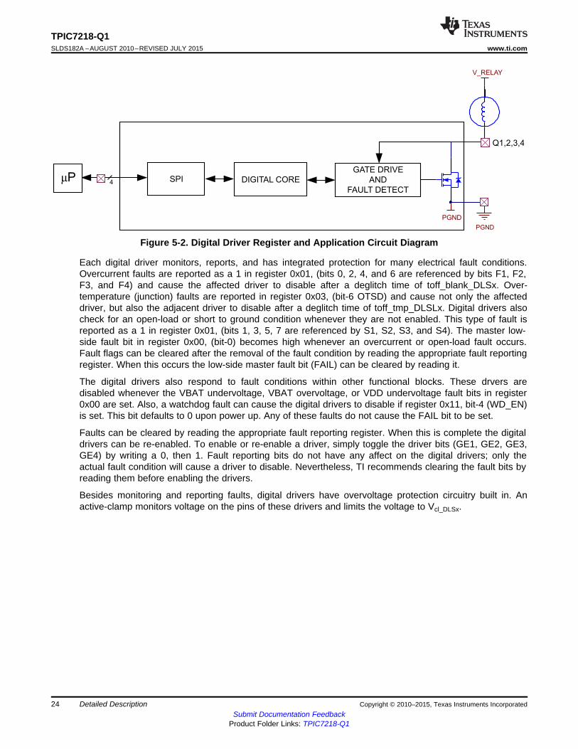
Figure 5-2. Digital Driver Register and Application Circuit Diagram
Each digital driver monitors, reports, and has integrated protection for many electrical fault conditions.Overcurrent faults are reported as a 1 in register 0x01, (bits 0, 2, 4, and 6 are referenced by bits F1, F2,F3, and F4) and cause the affected driver to disable after a deglitch time of toff_blank_DLSx. Over-temperature (junction) faults are reported in register 0x03, (bit-6 OTSD) and cause not only the affecteddriver, but also the adjacent driver to disable after a deglitch time of toff_tmp_DLSLx. Digital drivers alsocheck for an open-load or short to ground condition whenever they are not enabled. This type of fault isreported as a 1 in register 0x01, (bits 1, 3, 5, 7 are referenced by S1, S2, S3, and S4). The master low-side fault bit in register 0x00, (bit-0) becomes high whenever an overcurrent or open-load fault occurs.Fault flags can be cleared after the removal of the fault condition by reading the appropriate fault reportingregister. When this occurs the low-side master fault bit (FAIL) can be cleared by reading it.
The digital drivers also respond to fault conditions within other functional blocks. These drvers aredisabled whenever the VBAT undervoltage, VBAT overvoltage, or VDD undervoltage fault bits in register0x00 are set. Also, a watchdog fault can cause the digital drivers to disable if register 0x11, bit-4 (WD_EN)is set. This bit defaults to 0 upon power up. Any of these faults do not cause the FAIL bit to be set.
Faults can be cleared by reading the appropriate fault reporting register. When this is complete the digitaldrivers can be re-enabled. To enable or re-enable a driver, simply toggle the driver bits (GE1, GE2, GE3,GE4) by writing a 0, then 1. Fault reporting bits do not have any affect on the digital drivers; only theactual fault condition will cause a driver to disable. Nevertheless, TI recommends clearing the fault bits byreading them before enabling the drivers.
Besides monitoring and reporting faults, digital drivers have overvoltage protection circuitry built in. Anactive-clamp monitors voltage on the pins of these drivers and limits the voltage to Vcl_DLSx.
24 Detailed Description Copyright © 2010–2015, Texas Instruments IncorporatedSubmit Documentation Feedback
Product Folder Links: TPIC7218-Q1

( )( ) ( )DS ON MAX DPR DPR
VBAT I RDS VBAT I R- * > - *
SPI
DIGITAL CORE
µP
CHARGE PUMP
MOTOR GND
CPC
DPR
GPR
SPR
0 .1µF
V_BAT
IDPR
GPR
BG (2V)
COMP#1
COMP#2
GATE DRIVE
HSPC
4
RDPR
CCHP
V_BAT
TPIC7218-Q1www.ti.com SLDS182A –AUGUST 2010–REVISED JULY 2015
5.3.8 High-Side DriversThe TPIC7218-Q1 device features two independent high-side gate drivers to control and monitor externalN-Channel FETs. The pins, GPR, SPR, and DPR, are typically used to control an external N-MOSFET forthe purpose of providing power to a motor pump. The pins, GMR, SMR, and DMR are typically used tocontrol an external N-MOSFET for the purpose of providing power to the solenoid coils. When activated,the gate voltage drive on the GPR and GMR pins is sufficient to provide a strong VGS because of a built-incharge pump. High-side drivers are electrically protected and monitored for fault conditions.
5.3.8.1 High-Side Terminals: GPR, SPR, DPR, and HSPC
The GPR, SPR, and DPR (gate, source, and drain-pump relay) pins connect to an external N-MOSFET asshown in Figure 5-3. The purpose of this MOSFET is to relay the VBAT power to a pump motor. The N-MOSFET is turned on when the GPR pin is enabled. The GPR pin is controlled by either the HSPC pin orthe GE_PR bit, bit-3 of address 0x11 as listed in Table 5-4.
Figure 5-3. GPR, SPR, DPR, and HSPC Register and Application Circuit Diagram
Table 5-4. High-Side Operation Logic
HSPC PIN GE_PR BIT GPR GATE PINLOW 0 OFFLOW 1 ONHIGH 0 ONHIGH 1 ONOPEN 1 ONOPEN 0 OFF
The overcurrent detection of the external N-MOSFET is triggered by a voltage difference between theDPR and SPR pins in comparator COMP #1. To set the overcurrent threshold the external series resistor,RDPR, must be sized to generate a particular input voltage (in conjunction with IDPR) on one input of thecomparator. The other input voltage of the comparator changes as a function of the RDSON(MAX) and IDSvalues of the N-MOSFET. By comparing these voltages, the N-MOSFET overcurrent condition is reported.Given the RDSON(MAX) value of the N-MOSFET and the desired overcurrent threshold, RDPR can becalculated using Equation 2.
(2)
Copyright © 2010–2015, Texas Instruments Incorporated Detailed Description 25Submit Documentation Feedback
Product Folder Links: TPIC7218-Q1

VBAT
GPR
tGPRact
tGPRact tGPRact
TFovdet
Start Start
tGPRact
Overvoltage
TPIC7218-Q1SLDS182A –AUGUST 2010–REVISED JULY 2015 www.ti.com
If the VDS value of the N-MOSFET exceeds the threshold set by the comparator for more than thedeglitcher time, tOCdet, the GPR pin switches off and the appropriate fault flag (OCPR) is set high. Whenthe overcurrent condition ends, the GPR pin can be switched on again with the SPI enable bit or theexternal enable pin.
Faults detected on VDD, VBAT, Watchdog (if WD_EN bit is high) prevent the high-side driver fromenabling; GPR remains low or turns off. At the time the high-side driver is enabled, voltage on GPR pin istested for a short-to-ground condition only after a certain delay time defined as tSTGPR. If a short isdetected the GPR pin remains low. Any time the high-side driver is enabled overcurrent in the externalMOSFET, short-to-ground on GPR, and short-to-ground on SMR can cause a fault condition and disablethe high-side driver.
An overvoltage condition (such as load-dump) on VBAT turns the GPR pin on (clamping any energy fromthe alternator). If VBAT returns to normal operating voltage from an overvoltage fault condition, the GPRpin remains on for a minimum time, tGPRact.
If an overvoltage condition occurs on VBAT, the fault flag, FOV, is set after a deglitch time, tFovdet. With theovervoltage removed, the FOV flag can be cleared by reading address 0x00. After the fault bit is cleared,the GPR pin can be re-enabled. The GPR pin does not respond to successive overvoltage conditions untilafter a blanking time. See Table 5-5 and Figure 5-4 for more details.
Table 5-5. Pump Relay Fault and Operation
TPIC7218-Q1 STATESYSTEM EVENT FAULT BITS AFFECTED NOTESBEFORE AFTER EVENTEVENT
VDD Undervoltage PORn = 1 nRST is internally drivenGPR ON GPR OFF lowVBAT Overvoltage (>VovVBAT) FOV = 1 GPR OFF GPR ONVBAT Undervoltage (<VuvVBAT) FUV = 1 GPR ON GPR OFFWatchdog fault ( must be enabled) WDSTAT = 0, WD_FAULT = 1 GPR ON GPR OFF WD_EN = 1 (enabled)nRST pin externally driven low Erst = 1 GPR ON GPR OFFOvercurrent in motor OCPR=1,FHSD = 1 GPR ON GPR OFF OCPRDIS = 0 (disabled)Overcurrent in motor OCPR=1,FHSD = 1 GPR ON GPR ON OCPRDIS = 1 (enabled)Short to GND on GPR, while GPR is OFF FGPR = 1,FHSD = 1 FGPRDIS = 0 (disabled),GPR OFF GPR OFF(time > tSTGPR) turn ON GPRShort to GND on GPR, while GPR is ON FGPR = 1,FHSD = 1 GPR ON GPR OFF FGPRDIS = 0 (enabled)Short to GND on GPR, while GPR is OFF FGPR = 1,FHSD = 1 FGPRDIS = 1 (enabled),GPR OFF GPR ON(time > tSTGPR) turn ON GPRShort to GND on GPR, while GPR is ON FGPR = 1,FHSD = 1 GPR ON GPR ON FGPRDIS = 1 (enabled)Short to GND on SPR STGPR = 1,FHSD = 1 GPR ON GPR ON STGPRDIS = 1 (enabled)Short to GND on SPR STGPR = 1,FHSD = 1 GPR ON GPR OFF STGPRDIS = 0 (disabled)
Figure 5-4. Pump Relay High-Side Driver Overvoltage Behavior
The pump relay external MOSFET is electrically protected from voltage spikes by an active voltage clampthat limits any voltage levels between the GPR and SPR pins that are larger than Vgs_clamp.
26 Detailed Description Copyright © 2010–2015, Texas Instruments IncorporatedSubmit Documentation Feedback
Product Folder Links: TPIC7218-Q1

( )( ) ( )DS ON MAX DMR DMR
VBAT I RDS VBAT I R- * > - *
SPI
DIGITAL CORE
µP
CHARGE PUMP
5V
CPC
DMR
GMR
SMR
0 .1µF
V_BAT
RDMR
GMR
BG (2V)
COMP#1
COMP#2
GATE DRIVE
HSMC
4
V_RELAY
Q1,2,3,4,5,6,7,8
Low Side Drivers
I DMR
CCHP
V_BAT
V_RELAY
R SOL
TPIC7218-Q1www.ti.com SLDS182A –AUGUST 2010–REVISED JULY 2015
The GPR function supports PWM output. The charge on the charge-pump capacitor, CCHP, which is lostwhen GPR is switched on, is refreshed before the start of the next PWM cycle to a value that sufficientlyensures proper turnon behavior. The PWM capability consists of a period of T = 5 ms with a duty cycle10% to 90%. When selecting a duty cycle the rise and fall times of GPR must be taken into account.
5.3.8.2 High-Side Terminals: GMR, SMR, DMR, and HSMC
The GMR, SMR, and DMR (gate, source, and drain master relay) pins connect to an external N-MOSFETas shown in Figure 5-5. The purpose of this MOSFET is to relay VBAT power to a master power supplyfor solenoid coils. The N-MOSFET turns on when the GMR pin is enabled. The GMR pin function iscontrolled by either the HSMC pin or the GE_MR bit, bit-2 of address 0x11 as shown in Table 5-6.
Figure 5-5. GMR, SMR, DMR, and HSMC Register and Application Circuit Diagram
Table 5-6. High-Side Operation Logic
HSMC PIN GE_MR BIT GMR GATE PINLOW 0 OFFLOW 1 ONHIGH 0 ONHIGH 1 ONOPEN 1 ONOPEN 0 OFF
The overcurrent detection of the external N-MOSFET is triggered by a voltage difference between theDMR and SMR pins in comparator COMP #1. To set the overcurrent threshold, the external seriesresistor, RDMR, must be sized to generate a particular input voltage (in conjunction with IDMR) on one inputof the comparator. The other input voltage of the comparator changes as a function of the RDSON(MAX) andIDS values of the N-MOSFET. By comparing these voltages, the N-MOSFET overcurrent condition isreported. Given the RDSON(MAX) value of the N-MOSFET and the desired overcurrent threshold, RDMR canbe calculated using Equation 3.
(3)
Copyright © 2010–2015, Texas Instruments Incorporated Detailed Description 27Submit Documentation Feedback
Product Folder Links: TPIC7218-Q1

TPIC7218-Q1SLDS182A –AUGUST 2010–REVISED JULY 2015 www.ti.com
If the VDS of the N-MOSFET exceeds the threshold set by the comparator for more than the deglitchertime, tOCdet, the GMR pin switches off and the appropriate fault flag (OCMR) is set high. When theovercurrent condition ends, the GMR pin can be switched on again with the SPI enable bit or the externalenable pin.
Faults detected on VDD, VBAT, Watchdog (if WD_EN bit is high) prevent the high-side driver fromenabling; the GMR pin remains low or turns off. At the time the high-side driver is enabled, the voltage onthe GMR pin is tested for a short-to-ground condition only after a certain delay time defined as tSTGPR. If ashort is detected the GMR pin remains low. Any time the high-side driver is enabled overcurrent inMOSFET, short-to-ground on the GMR pin, and short-to-ground on the SMR pin can cause a faultcondition and disable the high-side driver.
An overvoltage condition (such as a load-dump) on VBAT either turns the GMR pin off or allows it toremain in the previous state depending on the setting of bit 5 (OV_GMR) in register 0x11. With theovervoltage removed, the fault flag FOV can be cleared by reading address 0x00.
The main relay external MOSFET is electrically protected from voltage spikes by an active voltage clampthat limits any voltage levels between GMR and SMR larger than Vgs_clamp.
Load-leakage faults are tested by sourcing a current, ILCdet, out of the SMR pin into the source of theexternal N-MOSFET. After a time, tLCdet, the SMR voltage is checked to see if it is above VDD. If noleakage is present, the source is above VDD and the GMR pin is turned on. If leakage is present, thesource is below VDD and the GMR pin does not turn on. A high on the LMR bit indicates a load-leakagefault. During a load-leakage fault, the SMR pin is biased to the voltage set by the external resistor (RSOL)and a series diode to VDD. Without this path, the SMR pin is floating and may not display faults properly.
Table 5-7 lists a summary of the faults that affect the GMR pin behavior.
Table 5-7. Master Relay Fault and Operation
TPIC7218-Q1 STATESYSTEM EVENT FAULT BITS AFFECTED NOTESBEFORE AFTER
EVENT EVENTnRST pin is internally drivenVDD Undervoltage PORn = 1 GMR ON GMR OFF low
VBAT Overvoltage (>VovVBAT) FOV = 1 GMR ON GMR OFF OV_GMR = 1VBAT Overvoltage (>VovVBAT) FOV = 1 GMR ON GMR ON OV_GMR = 0VBAT Undervoltage (<VuvVBAT) FUV = 1 GMR ON GMR OFF
WDSTAT = 0,Watchdog fault ( must be enabled) GMR ON GMR OFF WD_EN = 1 (enabled)WD_FAULT = 1nRST pin externally driven low Erst = 1 GMR ON GMR OFFOvercurrent in master relay OCMR=1,FHSD = 1 GMR ON GMR OFF OCMRDIS = 0 (disabled)Overcurrent in master relay OCMR=1,FHSD = 1 GMR ON GMR ON OCMRDIS = 1 (enabled)Short to GND on GMR, while GMR is OFF FGMRDIS = 0 (disabled),FGMR = 1,FHSD = 1 GMR OFF GMR OFF(time > tSTGMR) turn ON GMRShort to GND on GMR, while GMR is ON FGMR = 1,FHSD = 1 GMR ON GMR OFF FGMRDIS = 0 (disabled)Short to GND on GMR, while GMR is OFF FGMRDIS = 1 (enabled),FGMR = 1,FHSD = 1 GMR OFF GMR ON(time > tSTGMR) turn ON GMRShort to GND on GMR, while GMR is ON FGMR = 1,FHSD = 1 GMR ON GMR ON FGMRDIS = 1 (enabled)Short to GND on SMR STGMR = 1,FHSD = 1 GMR ON GMR OFF STGMRDIS = 0 (disabled)Short to GND on SMR STGMR = 1,FHSD = 1 GMR ON GMR ON STGMRDIS = 1 (enabled)
LGMRDIS = 0 (disabled),GMR is turned on while Q1-Q8 on LGMR = 1,FHSD = 1 GMR OFF GMR OFF turn ON GMRLGMRDIS = 1 (enabled),GMR is turned on while Q1-Q8 on LGMR = 1,FHSD = 1 GMR OFF GMR ON turn ON GMR
28 Detailed Description Copyright © 2010–2015, Texas Instruments IncorporatedSubmit Documentation Feedback
Product Folder Links: TPIC7218-Q1

TPIC7218-Q1www.ti.com SLDS182A –AUGUST 2010–REVISED JULY 2015
The high-side GMR, SMR, and DMR functionality also includes logic that facilitates system diagnostictesting. The operational status, as well as some fault conditions can be determined for both high-sidedrivers (HSD) and low-side drivers (LSD). Table 5-8 lists the details.
Table 5-8. High-Side Driver Logic (GMR Only)
HSD COMP #1 COMP #2LSD FETx RESULTFET (HSDC1) (HSDC2)ON OFF L L Normal operating condition for HSD FETON OFF H L HSD FET openON ON L L Normal operating condition for HSD and LSD FETsON ON H L HSD (GMR) FET in overcurrent conditionON ON H H HSD (GMR) FET in short to ground conditionOFF ON H H Normal operating condition for LSDOFF ON H L Open load or open LSD FETxOFF OFF H L Normal operating condition for HSD FETOFF OFF H H Load short to ground/LSD FETx short to ground
5.3.9 Wheel-Speed SensingThe TPIC7218-Q1 device is capable of interfacing with industry standard Active and Intelligent wheel-speed sensors. The TPIC7218-Q1 device features an analog front end that provides power, ground, andinterprets current-encoded speed and diagnostic information (Intelligent VDA sensors only) for sensors.Current thresholds can be adjusted to easily interface with most sensors. By setting a voltage on the VREFpin in conjunction with an appropriate current sense resistor, RLOAD, current levels through the wheel-speed sensors are evaluated according to the threshold states. Active wheel-speed sensor current pulselevels can be: undercurrent, overcurrent, wheel-speed-pulse-low (for example 7 mA), and wheel-speed-pulse-high (for example 14 mA). Intelligent wheel-speed sensor current pulse levels can be: undercurrent,overcurrent, wheel-speed-pulse-low (for example 7 mA), wheel-speed-pulse-high (for example 28 mA),and diagnostic-data-bit (for example 14 mA). Wheel-speed-pulse-low and wheel-speed-pulse-high logicstate is directly interpreted to a digital voltage output for each sensor (rotational speed). Diagnosticinformation, diagnostic-data-bit, is directly decoded and placed in four 9-bit registers. Rotational speedinformation (for two sensors) is also available on high-voltage open-drain outputs. Rotational wheel-speedpulse information for any of the sensors can be MUX-ed into a digital pulse counter. This counterincrements on both rising and falling edges. The 8-bit counter, along with other wheel-speed bits areavailable over SPI. Wheel-speed pins are also electrically protected from typical fault conditions. SeeFigure 5-6 for register and applications information.
Copyright © 2010–2015, Texas Instruments Incorporated Detailed Description 29Submit Documentation Feedback
Product Folder Links: TPIC7218-Q1

SPI
DIGITAL CORE
µP
CHARGE PUMP CPC
0 .1µF
CNT_EN
4
CNT_CLR
WSSOUT1/2/3/4
4
WHEEL SPEED
DIGITAL
PULSE
COUNTER
THRESHOLD
DETECTION
REFERENCE
CIRCUIT
GND
GND
4
GND
OPTIONAL
SYSTEM ESD
FILTER
4
4
RLOAD
WHEEL SPEED
SENSOR
INTERFACE
WSS1/2/3/4
WSP1/2/3/4
WSLS1/2/3/4
GND
VREF
WSSQ2
WSSQ1WSSOUT1
WSSOUT2
RWSSQ 1
RWSSQ 2
VDD
V_BAT
CLOAD
Wheel
Speed
Sensor
CCHP
C LOAD_WSPx
V_BAT
TPIC7218-Q1SLDS182A –AUGUST 2010–REVISED JULY 2015 www.ti.com
Figure 5-6. Wheel-Speed Register and Application Circuit Diagram
The TPIC7218-Q1 device has three pins for each of the four wheel-speed sensors. The WSPx pinsprovide a path for current from VBAT to the wheel-speed sensor. The WSLSx pins provide a path forcurrent from the wheel-speed sensor to GND. The WSSx pins monitor current through the sensor bymeasuring a voltage across the RLOAD resistance, shown in Figure 5-6.
Current is provided to the sensor from the WSP1, WSP2, WSP3, and WSP4 pins. When enabled (bysetting the WSPx bits in register 0x1B), the WSPx pins output current and are voltage clamped toVclamp_WSPx. WSPx pins are electrically protected from short-to-battery, short-to-ground, and overcurrent.Short-to-battery fault bits, WSPx_STB, are located in registers 0x08, 0x0A, 0x0C, 0x0E and overcurrentfault bits, WSPxILIMIT, are located in register 0x1D. If a fault is detected, then the WSPx pins disable.Reading these registers clears the fault bits after the fault condition has been removed.
Current from the sensors is returned to the WSP1, WSP2, WSP3, and WSP4 pins of the TPIC7218-Q1device, thus providing a path to ground. Current out of the sensor passes through a series resistor, RLOAD,into internal open-drain MOSFETs. These open-drain MOSFETs are controlled by setting the WSLSx bitsin register 0x1C. The WSLSx pins are electrically protected from overcurrent by detecting an excessivevoltage between WSLSx and WSSx pins. Overcurrent fault bits, WSSxOC, are located in register 0x0F. If afault is detected then the WSLSx pins stop sinking current. Reading these registers clears the fault bitsafter the fault is removed.
The sensed voltage difference between the WSSx and WSLSx pins provides the current encoded sensorinformation to the wheel-speed logic. The WSSx pins are electrically protected from short-to-battery andshort-to-ground. These conditions are reported by reading the WSSxOC and WSSxFAULT bits in register0x0F.
If a fault occurs on WSLSx, the path of the sensor to ground is removed. This type of fault must becleared by following a specific procedure to prevent an overcurrent fault from being erroneously reported.To clear this fault, first disable the WSPx pins, re-enable the WSLSx pins, and finally re-enable the WSPxpins. The main purpose for this procedure is to first provide a ground path for the sensor before providingpower. Other types of faults can be cleared in the normal way, as long as the WSLSx pins are enabled.Table 5-9 lists more information about wheel-speed faults.
30 Detailed Description Copyright © 2010–2015, Texas Instruments IncorporatedSubmit Documentation Feedback
Product Folder Links: TPIC7218-Q1

TPIC7218-Q1www.ti.com SLDS182A –AUGUST 2010–REVISED JULY 2015
Table 5-9. Wheel-Speed Sense Fault and Operation
TPIC7218-Q1SYSTEM EVENT FAULT BITS AFFECTED NOTESPRIOR TO POST EVENTEVENT
WSPx ON WSPx OFF All of the enable bits for theseVDD Undervoltage PORn = 1 WSLSx ON WSLSx OFF functions are cleared. nRST is driven
WSSQx ON WSSQx OFF low.WSPx ON WSPx OFF All of the enable bits for theseVBAT Overvoltage FOV = 1 WSLSx ON WSLSx OFF functions are cleared(>VovVBAT) WSSQx ON WSSQx OFFWSPx ON WSPx OFF All of the enable bits for thesenRST pin externally driven Erst = 1 WSLSx ON WSLSx OFF functions are clearedlow WSSQx ON WSSQx OFF
WSSQx and WSLSx remain on butWSPx ON WSPx OFF no wheel-speed output is producedOvercurrent in WSPx WSPxILIMIT = 1 WSLSx ON WSLSx ON because the sensor has no power.WSSQx ON WSSQx ON The enable bits for WSPx remain 1WSPx and WSSQx remain on but noWSPx ON WSPx ON wheel-speed output is producedOvercurrent in WSSx-WSLSx WSSxOC = 1 WSLSx ON WSLSx OFF because the sensor has no ground.WSSQx ON WSSQx ON The enable bits for WSLSx remain 1
WSPx ON WSPx ON WSLSx and WSPx remain on. TheOvercurrent in WSSQx WSSQxILIMIT = 1 WSLSx ON WSLSx ON enable bits for WSSQx remain 1
WSSQx ON WSSQx OFFThis fault is detected only whileWSPx OFF WSPx OFF WSPx are OFF. WSLSx and WSSQxShort to VBAT on WSPx WSPx_VBAT = 1 WSLSx ON WSLSx ON remain unaffected while WSPx is onWSSQx ON WSSQx ON and shorted to VBAT.WSSQx and WSPx remain on;
WSPx ON WSPx ON wheel-speed outputs may beShort to GND on WSLSx WSSxFAULT = 1 WSLSx ON WSLSx ON produced but the wheel-speed
WSSQx ON WSSQx ON ground path is not throughTPIC7218-Q1 anymoreThis fault is detected only whileWSPx ON WSPx ON WSSQx are off. WSPx and WSLSxShort to GND on WSSQx WSSQxFAULT = 1 WSLSx ON WSLSx ON remain on and wheel-speed outputsWSSQx OFF WSSQx OFF can still be observed.
Copyright © 2010–2015, Texas Instruments Incorporated Detailed Description 31Submit Documentation Feedback
Product Folder Links: TPIC7218-Q1

TPIC7218-Q1SLDS182A –AUGUST 2010–REVISED JULY 2015 www.ti.com
The wheel-speed internal equivalent model, shown in Figure 5-7 and Figure 5-8, describe how thisfunctional block works. Users need only select a wheel-speed sensor, current sense resistor, RLOAD, andVREF voltage for basic operation. The wheel-speed functionality is designed to accommodate both Activeand Intelligent sensors; the WSSTYPE bit in register 0x1D must be set appropriately.
Figure 5-7. Internal Diagram Using Intelligent Type Sensor (WssTYPE = 0)
Table 5-10. Intelligent Sensor Wheel-Speed Thresholds
PERCENTAGE OF MAXIMUMTHRESHOLD SIGNIFICANCE THRESHOLD (1)
ISENSOR > ITHRESH4VTHRESH4 100% (40 mA)Overcurrent (possible short to battery)ITHRESH4 > ISENSOR > ITHRESH3VTHRESH3 50% (20 mA)Rotational Wheel-Speed Logic- HighITHRESH3 > ISENSOR > ITHRESH2VTHRESH2 25% (10 mA)Diagnostic sensor Information (9-bit)
ISENSOR < ITHRESH1VTHRESH1 11.25% (4.5 mA)Undercurrent (possible short to ground)
(1) The current is based on maximum of 40 mA, RLOAD OF 50 Ω, and VREF of 2 V
32 Detailed Description Copyright © 2010–2015, Texas Instruments IncorporatedSubmit Documentation Feedback
Product Folder Links: TPIC7218-Q1

( )REF LOAD WSS over currentV R I
-= *
TPIC7218-Q1www.ti.com SLDS182A –AUGUST 2010–REVISED JULY 2015
Figure 5-8. Internal Diagram Using Active Type Sensor (WssTYPE = 1)
Table 5-11. Active Sensor Wheel-Speed Thresholds
THRESHOLD SIGNIFICANCE PERCENTAGE OF MAXIMUM THRESHOLD (1)
ISENSOR > ITHRESH4 100% (20 mA)VTHRESH4 *Not used *Not usedISENSOR > ITHRESH3VTHRESH3 100% (20 mA)Overcurrent (possible short to battery)
ITHRESH3 > ISENSOR > ITHRESH2VTHRESH2 50% (10 mA)Rotational wheel-speed logic- highISENSOR < ITHRESH1VTHRESH1 22.5% (4.5 mA)Undercurrent (possible short to ground)
(1) The current is based on maximum of 40 mA, RLOAD OF 50 Ω, and VREF of 2 V.
Both types of sensors provide information based on varying current levels. The TPIC7218-Q1 deviceprovides a way to select different current thresholds by adjusting a voltage on the VREF pin. Internally, thevoltage on VREF governs all four thresholds in a ratio metric manner. VREF voltage actually sets themaximum threshold (100%), then, all the other thresholds are automatically set. Intelligent sensors requireITHRESH4 to be set to the maximum threshold, IWSS(overcurrent), and Active sensors require ITHRESH3 to be setto the maximum threshold. For both Intelligent sensors (requiring four thresholds) and Active sensors(requiring three thresholds) use Equation 4 to select a value for VREF.
(4)
Copyright © 2010–2015, Texas Instruments Incorporated Detailed Description 33Submit Documentation Feedback
Product Folder Links: TPIC7218-Q1

ITHRESH1
ITHRESH2
ITHRESH3
0
7
14
mA
time
Active Wheel Speed Sensor
22.5%
50%
100%
ITHRESH1
ITHRESH2
ITHRESH3
ITHRESH4
0
7
14
28
mA
time
11.25%
25%
50%
Intelligent Wheel Speed Sensor100%
TPIC7218-Q1SLDS182A –AUGUST 2010–REVISED JULY 2015 www.ti.com
For example, a typical Intelligent wheel-speed sensor may have a maximum typical current less than 40mA. This 40-mA current must be set to correspond to VTHRESH4 (100%). If the value of RLOAD is selectedas 50 Ω, then the resulting VREF voltage is calculated to be 2 V. Similarly, a typical Active wheel-speedsensor may have a maximum typical current less than 20 mA. This 20-mA current must be set tocorrespond to VTHRESH3 (100%). However, by setting the WSSTYPE bit, the digital decoder uses VTHRESH3threshold to actually determine if an overcurrent condition is occurring. By effectively removing theVTHRESH4 resistor in the comparator resistor chain, shown in Figure 5-9, a VREF voltage of 2.4 V and anRLOAD of 120 Ω, are needed to properly set the current thresholds. The ratio of the resistor chain did notchange, however the current threshold detection levels did. See Figure 5-9 for more detail.
Figure 5-9. Example Wheel-Speed Current Pulse Diagram
While selecting RLOAD and VREF, care must be taken so that all electrical specification values are notviolated. When the maximum current threshold is selected, the other three thresholds are automaticallyset.
During normal operation, the WSSOUTx pins provide a digital signal that is high whenever sensor currentcreates a voltage drop across RLoad that is above the VTHRESH3 level for intelligent sensors and VTHRESH2level for Active sensors. If the current is less than these respective thresholds, the WSSOUTx pins returnto ground. The WSSQ1 and WSSQ2 pins are open-drain outputs that reproduce signals on theWSSOUT1 and WSSOUT2 pins after a propagation delay time of twss_delay. A high level on WSSOUT1 orWSSOUT2 results in low level on WSSQ1 or WSSQ2 pin. These two pins are useful for providing wheel-speed information in a high voltage signal form. The WSSQ1 and WSSQ2 pins also have short-to-groundand open-load detection functionality. The WSSQxFAULT and WSSQxILIMIT bits in register 0x05 report thesefaults and are cleared by reading them after the removal of the fault condition. During an overcurrent faultthe WSSQ1 and WSSQ2 pins remain enabled for a time of tdelay_WSSQx. After this time these pins aredisabled.
The TPIC7218-Q1 device also features an 8-bit wheel-speed pulse counter. This counter increments onevery rising and falling edge of a selected WSSOUTx. A MUX selects which the WSSOUTx signal is inputto the counter; bits WS_Cnt_MUX[1] and WS_Cnt_MUX[0] program the MUX as listed in Table 5-12.Count data is reported in register 0x04. A high on the CNT_EN pin allows the counter to increment. A highon the CNT_CLR pin forces the counter to reset to 0. The count value is available for read through SPI atany point. If the counter is allowed to reach maximum value, the count value remains at maximum but anoverflow bit, WSS_OV_Cnt is set. If both CNT_CLR and CNT_EN pins are in a high logic state then theWS_Fail_Cnt bit is set. These bits clear on read after the fault conditions have been removed.
Table 5-12. Wheel-Speed Counter Input
WS_Cnt_MUX[1] WS_Cnt_MUX[0] SELECTED INPUT0 0 WSSOUT11 0 WSSOUT20 1 WSSOUT31 1 WSSOUT4
34 Detailed Description Copyright © 2010–2015, Texas Instruments IncorporatedSubmit Documentation Feedback
Product Folder Links: TPIC7218-Q1

DIGITAL COREµP ISO-KKTx
KRx K-LINE
DRIVER/
RECEIVER
DIAGNOSTIC
EQUIPMENT
V_BAT
TPIC7218-Q1www.ti.com SLDS182A –AUGUST 2010–REVISED JULY 2015
When the TPIC7218-Q1 device is paired with VDA protocol compatible Intelligent wheel-speed sensors,additional functionality for processing and reporting diagnostic information can be enabled. Diagnosticencoded data (Manchester encoded) in the form of current pulses reaching the ITHRESH2 (10 mA) thresholdare decoded and placed in the WSSxDx bits. All nine bits are available for reading. If any of the (nine) bitpulse widths were outside the allowed pulse width range (36 μs to 64 μs including variations) then thepulse widths are not counted as valid. As each of the nine bits are input, only valid bits cause theWSSx_Valid counter to increment. In this way information about bit errors, or fewer than nine bits beingsent from the sensor is recorded and available for each wheel-speed channel. The TPIC7218-Q1 devicealso contains logic to determine when a new 9-bit frame has started to be input. When detected, theWSSx_New bit is set. If the wheel-speed sensor is in stand still mode then the TPIC7218-Q1 devicedetects this current pulse activity, resulting in the WSS_MODE bit being set. Both of these bits can becleared upon read.
5.3.10 K-LineThe TPIC7218-Q1 device includes a serial communication transceiver for K-Line. K-Line provides a bi-directional half-duplex interface for automotive diagnostic communication with data transfer rates of up to10.4 kbps. The integrated transceiver conforms to the ISO-9141 standard and meets the on-boarddiagnostic (OBD) requirements of the California Air Resources Board (CARB). For more information onthe K-Line protocol see the compete K-Line standard.
Features of the K-Line module include the following:• ISO-K operates over a wide signal voltage range and is capable of driving high currents.• ISO-K pin can tolerate a parasitic capacitance of up to 10 nF.• ISO-K pin is electrically protected to withstand short-to-ground and overcurrent faults.• The driver stage of the ISO-K pin is thermally protected. A temperature fault disables the bus. Thermal
protection also includes hysteresis and blank time before restarting.• KRx and KTx directly interface to both 5-V and 3.3-V microprocessors without the need for pullup
resistors.• K-Line continues to function regardless of any TPIC7218-Q1 fault conditions with the exception of VDD
undervoltage reset condition which powers down the entire TPIC7218-Q1 device.
Figure 5-10. K-Line Application Schematic
Copyright © 2010–2015, Texas Instruments Incorporated Detailed Description 35Submit Documentation Feedback
Product Folder Links: TPIC7218-Q1

SPI
DIGITAL CORE
µP
nRST
4
WATCHDOG
LOW VOLTAGE WARNING
LAMP DRIVER
WL_LS
VIO
WDin
WLQ2
WLQ1
VBAT
WLG2
WLG1
VBAT
TPIC7218-Q1SLDS182A –AUGUST 2010–REVISED JULY 2015 www.ti.com
5.3.11 Warning Lamp DriversThe TPIC7218-Q1 device features three output pins for warning lamps. The WLQ1 and WLQ2 pins arehigh voltage low-side drivers. The WL_LS pin is a low voltage low-side driver.
The WL_LS driver enables whenever the watchdog controlled bit, WD_STAT, is high. This low-side driveris an open-drain MOSFET; to realize a high logic level and external pullup resistor must be used. Driveroperation is only dependent on a watchdog fault.
The WLQ1 driver enables whenever the WLG1 pin and the GE_9 bit is set. The WLQ2 driver works in thesame way utilizing the WLG2 pin and the GE_10 bit. Each driver is monitored for three fault conditions:overcurrent, open-load, and over-temperature. However, driver operation also depends on other faultconditions: VDD undervoltage, and watchdog fault. See the application circuit and register diagram inFigure 5-11.
Figure 5-11. Warning Lamp Driver Register and Application Circuit Diagram
Each digital driver monitors, reports, and has integrated protection for many electrical fault conditions.Overcurrents are reported as a 1 in register 0x03, (bits 0 and 2 are referenced by bits F9, F10) and do notcause the affected driver to disable. Overcurrents are merely reported after a deglitch time of toff_blank_WLQx.Over-temperature (junction) faults are reported in register 0x03, (bit-6 OTSD) and cause both drivers todisable after a deglitch time of toff_tmp_WLQx.. The high-voltage warning-lamp drivers are also checked for anopen-load or short to ground condition whenever they are not enabled. This type of fault causes register0x03, (bits 1 and 3 are referenced by bits S9 and S10) to be reported as a 1. A master low-side fault bit inregister 0x00, (bit-0) becomes high whenever an overcurrent or open-load fault occurs. Faults can becleared by reading the appropriate fault reporting register. When this occurs, the low-side master fault bit(FAIL) can be cleared by reading it.
The high-voltage warning-lamp drivers also respond to fault conditions within other functional blocks.These drivers are disabled whenever the VDD undervoltage fault bit in register 0x00 is set. Also, awatchdog fault can cause these drivers to disable, if register 0x11, bit-4 (WD_EN) is set. This bit defaultsto 0 upon power up. Any of these faults do not cause the FAIL bit to be set.
Faults can be cleared by reading the appropriate fault reporting register. When this occurs the digitaldrivers can be re-enabled. Fault reporting bits do not have any affect on these warning lamp drivers; onlythe actual fault condition causes a driver to disable. Nevertheless, TI recommends clearing the fault bitsby reading them before enabling the drivers.
36 Detailed Description Copyright © 2010–2015, Texas Instruments IncorporatedSubmit Documentation Feedback
Product Folder Links: TPIC7218-Q1

TPIC7218-Q1www.ti.com SLDS182A –AUGUST 2010–REVISED JULY 2015
Aside from monitoring and reporting faults, the high-voltage warning-lamp drivers have overvoltageprotection circuitry built in. An active-clamp monitors voltage on the pins of these drivers. Voltages largerthan Vcl_WLQx are clamped.
5.3.12 Watchdog OperationThe TPIC7218-Q1 device also features watchdog functionality. Watchdog functionality is programmableand can be disabled. This functional block receives clock pulses from an external microprocessor throughWDIN pin to verify proper system operation. Whenever a watchdog fault occurs, the low-voltage warning-lamp pin (WL_LS), the reset pin (nRST), and many of the other functional blocks within the TPIC7218-Q1device are affected. The TPIC7218-Q1 device can be set to accept a range of different pulse widths foreasy connection to most microprocessors.
If watchdog functionality is enabled (WD_EN = 1), the TPIC7218-Q1 logic monitors WDIN pulse widths bycounting the number of internal clocks that occur between WDIN rising and falling edges. Two, 2-bitvalues ( WDH<1:0>, WDL<1:0>) can be adjusted to select the length of a valid window range for a WDINpulse. Pulse widths inside of this window range are counted as a good pulse. A good pulse increments a3-bit state machine counter by one (WDCNTx bits, in register 0x05). When a counter value of 7 isreached, the status bit, WDSTAT , becomes a 1 and all TPIC7218-Q1 watchdog inhibited functionality isenabled. If a bad pulse occurs then the state machine counter is decremented by three. The WD_FAULTbit is set whenever the counter value is 0, causing the WD_STAT bit to become low. A fault turns off high-side drivers, low-side drivers, wheel-speed functionality, and high-voltage warning-lamp drivers. Both thelow-voltage warning-lamp driver (WL_LS) and the reset pin (nRST) enables. The SPI continues to functionand the WD_FAULT and WDSTAT bits indicate a watchdog fault. When a full watchdog count is reached,register bits and functionality would return to normal state. Refer to Figure 5-12 through Figure 5-14 formore details on the state transitions and timing.
If the WDIN pin does not realize a transition after twice the length of time selected in the upper window,which is set by bits WDH<1:0>, then an out-of-range condition occurs. The watchdog fault becomes highand the watchdog status bit becomes low (WD_FAULT = 1, and WDSTAT = 0).
Copyright © 2010–2015, Texas Instruments Incorporated Detailed Description 37Submit Documentation Feedback
Product Folder Links: TPIC7218-Q1

InternalClock
WDin
Lower Window
Upper Window
Out-of-range Window
InternalClock
WDin
Lower Window
Upper Window
Out-of-range Window
InternalClock
WDin
Lower Window
Upper Window
Out-of-range Window
000
Stat=0
001
010
011
100
101
110*
111
Stat=1
good
good
good
good
good
good
bad
bad
bad
bad
bad
bad
bad
out-of-rangeRST
Single pulse
on transition to 000A
Aout-of-range
Aout-of-range
Aout-of-range
Aout-of-range
Aout-of-range
Aout-of-range
Aout-of-range
(*CNT value on PUC)
TPIC7218-Q1SLDS182A –AUGUST 2010–REVISED JULY 2015 www.ti.com
Figure 5-12. Watchdog State Transition Diagram
Figure 5-13. Timing Diagram Showing A Bad Pulse
Figure 5-14. Timing Diagram Showing A Good Pulse
38 Detailed Description Copyright © 2010–2015, Texas Instruments IncorporatedSubmit Documentation Feedback
Product Folder Links: TPIC7218-Q1

TPIC7218-Q1www.ti.com SLDS182A –AUGUST 2010–REVISED JULY 2015
5.4 Device Functional ModesThe device operates in normal mode as described in Section 5.3 unless it is in the reset state.
5.4.1 Device ResetSeveral events cause the TPIC7218-Q1 device to reset. For a compete view of TPIC7218-Q1 behaviorduring reset, refer to Table 5-1.
Power-On Reset A power-on reset, POR, is caused when the VDD supply voltage falls below the resetthreshold. On POR the nRST pin is pulled low by the TPIC7218-Q1 device.
Watchdog Reset A watchdog reset is initiated whenever the Watchdog counter decrements to 000. UponWatchdog Reset, the nRST pin is pulsed low, and the WDSTAT flag is cleared. As the nRSTpin is released, the Watchdog state machine is restarted. The watchdog will re-enable after adelay time TWD_PULSE to allow sufficient time for the microcontroller to reset.
External Reset An external reset is realized whenever the nRST pin is driven low by an external signal(usually from a microprocessor). When nRST is released the Erst bit is set, indicating that anexternal reset occurred.
5.5 Programming
5.5.1 Serial Peripheral Interface (SPI) Interface To MicrocontrollerThe TPIC7218-Q1 device uses a SPI communication interface. The TPIC7218-Q1 device operates as aslave with full-duplex, synchronous, 8-bit transfer frames. The device can be controlled and monitored inone of three modes: Read, Write, and Dummy. Read command returns data to the master. If a faultregister is read, then any faults will be cleared. However, if the fault still exists then the fault reportingbit(s) will remain high. A write command sends data to the slave. Data is latched in on the rising edge ofthe second chip select. A dummy command is used whenever the master and slave loosesynchronization. This happens whenever the master does not issue a normal 16 bit transfer using twoeight bit frames. Dummy commands essentially reset the SPI logic to the default state.
A typical SPI operation contains two full chip select frames; each containing eight clock pulses. All SPItransaction starts when CSN transitions to a logic low. During this time 8-bits of mode, R/W, and addressdata are clocked into SI. Finally, the CSN returns high, concluding the first half of the normal transaction.The second half of the normal transaction starts when CSN again transitions to a logic low. During thistime 8-bits of data are clocked into SI. Finally, the CSN returns high, and a normal SPI transaction isconcluded. If one chip-select frame does not have exactly eight clocks, then the whole 16-bit transaction isconsidered invalid and is ignored. The CSN must go high for a window of 2 μs to 28 μs (CSNtimeout)between two 8-bit commands for the 16-bit command to be considered valid. A 16-bit read commandconsists of an 8-bit read command of the intended address and an 8-bit dummy command. The SPI canalso operate in burst mode, whereby consecutive 8-bit read commands result in a consecutive 8-bit databeing returned to the master.
Table 5-13. SPI Instruction Encoding
MODE R/Wn STAT. A[5] A[4] A[3] A[2] A[1] A[0]Unused 0 1 A[5] A[4] A[3] A[2] A[1] A[0]Read 1 0 A[5] A[4] A[3] A[2] A[1] A[0]Write 0 0 A[5] A[4] A[3] A[2] A[1] A[0]
Dummy 1 1 X X X X X X
Copyright © 2010–2015, Texas Instruments Incorporated Detailed Description 39Submit Documentation Feedback
Product Folder Links: TPIC7218-Q1

TPIC7218-Q1SLDS182A –AUGUST 2010–REVISED JULY 2015 www.ti.com
Figure 5-15. One Chip-Select Frame
The SO pin contains the register data in response to the previous eight bit frame. Data out is alwaysdelayed by one SPI transfer (for example, response to the command N is shifted out at the same timecommand N+1 is shifted in). Valid data is shifted out from the SO pin on the rising edge of SCLK. Theresponse to the SPI frame depends on which type of transaction mode is requested by the Master (read,write, or dummy).
If the SPI transaction is valid, the Slave determines what type of operation is being requested. If a Readtransaction is requested, the Slave responds with the Read byte during the next SPI transaction. Figure 5-16 shows the SPI Read operation.
Figure 5-16. One Chip-Select Frame
A Write operation places the data byte into the address specified in the previous chip select frame.
Figure 5-17. One Chip-Select Frame
5.5.1.1 Summary and Description Of Control and Reporting Registers
The TPIC7218-Q1 device contains 30 registers that contain both fault reporting and control bits. Refer tothe following tables for register map and functional description of each bit.
40 Detailed Description Copyright © 2010–2015, Texas Instruments IncorporatedSubmit Documentation Feedback
Product Folder Links: TPIC7218-Q1

TPIC7218-Q1www.ti.com SLDS182A –AUGUST 2010–REVISED JULY 2015
5.6 Register Maps
5.6.1 SPI Registers
Table 5-14. SPI Registers Map
ADDRESS R/W b7 b6 b5 b4 b3 b2 b1 b0
0x00 R HSDC2 FHSD FOV FUV Erst HSDC1 PORn FAIL
0x01 R S4 F4 S3 F3 S2 F2 S1 F1
0x02 R S8 F8 S7 F7 S6 F6 S5 F5
0x03 R WS_OV_Cnt OTSD WS_Fail_Cnt KI S10 F10 S9 F9
0x04 R WS_Cnt_OUT7 WS_Cnt_OUT6 WS_Cnt_OUT5 WS_Cnt_OUT4 WS_Cnt_OUT3 WS_Cnt_OUT2 WS_Cnt_OUT1 WS_Cnt_OUT0
0x05 R WSSQ2ILIMIT WSSQ1ILIMIT WSSQ2FAULT WSSQ1FAULT WDSTAT WDCNT2 WDCNT1 WDCNT0
0x06 R VLDDEG OCPR STGPR FGPR LMR FGMR STGMR OCMR
0x07 R WSS1D7 WSS1D6 WSS1D5 WSS1D4 WSS1D3 WSS1D2 WSS1D1 WSS1D0
0x08 R WSS1_Valid3 WSS1_Valid2 WSS1_Valid1 WSS1_Valid0 WSP1_STB WSS1_Mode WSS1_New WSS1D8
0x09 R WSS2D7 WSS2D6 WSS2D5 WSS2D4 WSS2D3 WSS2D2 WSS2D1 WSS2D0
0x0A R WSS2_Valid3 WSS2_Valid2 WSS2_Valid1 WSS2_Valid0 WSP2_STB WSS2_Mode WSS2_New WSS2D8
0x0B R WSS3D7 WSS3D6 WSS3D5 WSS3D4 WSS3D3 WSS3D2 WSS3D1 WSS3D0
0x0C R WSS3_Valid3 WSS3_Valid2 WSS3_Valid1 WSS3_Valid0 WSP3_STB WSS3_Mode WSS3_New WSS3D8
0x0D R WSS4D7 WSS4D6 WSS4D5 WSS4D4 WSS4D3 WSS4D2 WSS4D1 WSS4D0
0x0E R WSS4_Valid3 WSS4_Valid2 WSS4_Valid1 WSS4_Valid0 WSP4_STB WSS4_Mode WSS4_New WSS4D8
0x0F R WSS4OC WSS3OC WSS2OC WSS1OC WSS4FAULT WSS3FAULT WSS2FAULT WSS1FAULT
0x10 RW GE8 GE7 GE6 GE5 GE4 GE3 GE2 GE1
0x11 RW WD_Fault 0 OV_GMR WD_EN GE_PR GE_MR GE10 GE9
0x12 RW WDH<1> WDH<0> WDL<1> WDL<0> PWMFreq1 PWMFreq0 WS_Cnt _MUX[1] WS_Cnt _MUX[0]
0x13 RW PWMQ5<7> PWMQ5<6> PWMQ5<5> PWMQ5<4> PWMQ5<3> PWMQ5<2> PWMQ5<1> PWMQ5<0>
0x14 RW 0 0 0 0 PWMQ5Phase<1> PWMQ5Phase<0> PWMQ5<9> PWMQ5<8>
0x15 RW PWMQ6<7> PWMQ6<6> PWMQ6<5> PWMQ6<4> PWMQ6<3> PWMQ6<2> PWMQ6<1> PWMQ6<0>
0x16 RW 0 0 0 0 PWMQ6Phase<1> PWMQ6Phase<0> PWMQ6<9> PWMQ6<8>
0x17 RW PWMQ7<7> PWMQ7<6> PWMQ7<5> PWMQ7<4> PWMQ7<3> PWMQ7<2> PWMQ7<1> PWMQ7<0>
0x18 RW 0 0 0 0 PWMQ7Phase<1> PWMQ7Phase<0> PWMQ7<9> PWMQ7<8>
0x19 RW PWMQ8<7> PWMQ8<6> PWMQ8<5> PWM4Q8<4> PWMQ8<3> PWMQ8<2> PWMQ8<1> PWMQ8<0>
0x1A RW 0 0 0 0 PWMQ8Phase<1> PWMQ8Phase<0> PWMQ8<9> PWMQ8<8>
0x1B RW 0 WSSP4 WSSP3 WSSP2 WSSP1 WSSTYPE WSSQ2 WSSQ1
0x1C RW OCPRDIS STGPRDIS OCMRDIS STGMRDIS WSLS4 WSLS3 WSLS2 WSLS1
0x1D RW/R* VREFOK* FGPRDIS FGMRDIS LMRDIS WSP4ILIMIT WSP3ILIMIT* WSP2ILIMIT* WSP1ILIMIT*
Copyright © 2010–2015, Texas Instruments Incorporated Detailed Description 41Submit Documentation Feedback
Product Folder Links: TPIC7218-Q1

TPIC7218-Q1SLDS182A –AUGUST 2010–REVISED JULY 2015 www.ti.com
Table 5-15. Description Of Control and Reporting Bits
BIT NAME DESCRIPTION
Any fault on any digital or PWM low-side driverFail 0 = Fault not detected
1 = Fault detected
Power-on reset. Reset low when read by microcontroller.PORn 0 = No power-on reset detected. Reset to this value when read by microcontroller.
1 = Power-on reset detected
High-side driver comparator1 for Master Relay (MR)HSDC1 0 = Comparator output low
1 = Comparator output high
RST pin is pulled low by external sourceErst 0 = Fault not detected
1 = Fault detected
Undervoltage on VBATFuv 0 = Fault not detected
1 = Fault detected
Overvoltage on VBATFov 0 = Fault not detected
1 = Fault detected
Any fault on the high-side drivers (either GMR or GPR). If set, this bit is latched until Address 6 is read. Then, itclears on read.FHSD
0 = Fault not detected1 = Fault detected
High-side driver comparator 2 for Master Relay (MR)HSDC2 0 = Comparator output low
1 = Comparator output high
Open-load fault on the low-side output (S9 reports WLQ1 fault and S10 reports WLQ2 fault)Sx 0 = Fault not detected on output x
1 = Fault detected on output x
Short-to-battery fault on the low-side output (F9 reports WLQ1 fault and F10 reports WLQ2 fault)Fx 0 = Fault not detected on output x
1 = Fault detected on output x
CNT_EN and CNT_CLR set at the same timeWS_Fail_Cnt 0 = Fault not detected
1 = Fault detected
Status bit for Kline current limit conditionKl 0 = Fault not detected
1 = Fault detected
Any overtemperature faultOTSD 0 = Fault not detected
1 = Fault detected
Count overflow on the wheel-speed sensor (past 256)WS_OV_Cnt 0 = Overflow not detected
1 = Overflow detected
42 Detailed Description Copyright © 2010–2015, Texas Instruments IncorporatedSubmit Documentation Feedback
Product Folder Links: TPIC7218-Q1

TPIC7218-Q1www.ti.com SLDS182A –AUGUST 2010–REVISED JULY 2015
Table 5-15. Description Of Control and Reporting Bits (continued)BIT NAME DESCRIPTION
WSSx_Valid4 This word shows the valid number of bits in each wheel-speed channel.WSSx_Valid3WSSx_Valid2WSSx_Valid1
WDCNT0 Status Bit 1 of three that is used to track the operation of the watchdog circuit (LSB)WDCNT1 Status Bit 2 of three that is used to track the operation of the watchdog circuitWDCNT2 Status Bit 3 of three that is used to track the operation of the watchdog circuit (MSB)
Watchdog status bitWDSTAT 0 = Out-of-range
1 = In-range
Open load or short to ground on WSSQ1WSSQ1FAULT 0 = Fault not detected
1 = Fault detected
Open load or short to ground on WSSQ2WSSQ2FAULT 0 = Fault not detected
1 = Fault detected
Overcurrent on WSSQ1WSSQ1ILIMIT 0 = Fault not detected
1 = Fault detected
Overcurrent on WSSQ2WSSQ2ILIMIT 0 = Fault not detected
1 = Fault detected
Overcurrent fault on MROCMR 0 = Fault not detected
1 = Fault detected
Short-to-ground fault on MRSTGMR 0 = Fault not detected
1 = Fault detected
GMR disabled by external circuitryFGMR 0 = GMR not disabled
1 = GMR disabled
Load-leakage fault on MR (Master Relay)LMR 0 = Fault not detected
1 = Fault detected
GPR disabled by external circuitryFGPR 0 = GPR not disabled
1 = GPR disabled
Short-to-ground fault on PRSTGPR 0 = Fault not detected
1 = Fault detected
Overcurrent fault on PROCPR 0 = Fault not detected
1 = Fault detectedVLD DEG This bit is a replica of FOVWSS1Dx VDA data bits for wheel-speed channel 1
Copyright © 2010–2015, Texas Instruments Incorporated Detailed Description 43Submit Documentation Feedback
Product Folder Links: TPIC7218-Q1
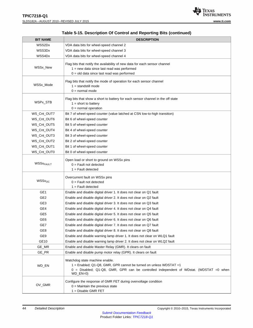
TPIC7218-Q1SLDS182A –AUGUST 2010–REVISED JULY 2015 www.ti.com
Table 5-15. Description Of Control and Reporting Bits (continued)BIT NAME DESCRIPTIONWSS2Dx VDA data bits for wheel-speed channel 2WSS3Dx VDA data bits for wheel-speed channel 3WSS4Dx VDA data bits for wheel-speed channel 4
Flag bits that notify the availability of new data for each sensor channelWSSx_New 1 = new data since last read was performed
0 = old data since last read was performed
Flag bits that notify the mode of operation for each sensor channelWSSx_Mode 1 = standstill mode
0 = normal mode
Flag bits that show a short to battery for each sensor channel in the off stateWSPx_STB 1 = short to battery
0 = normal operationWS_Cnt_OUT7 Bit 7 of wheel-speed counter (value latched at CSN low-to-high transition)WS_Cnt_OUT6 Bit 6 of wheel-speed counterWS_Cnt_OUT5 Bit 5 of wheel-speed counterWS_Cnt_OUT4 Bit 4 of wheel-speed counterWS_Cnt_OUT3 Bit 3 of wheel-speed counterWS_Cnt_OUT2 Bit 2 of wheel-speed counterWS_Cnt_OUT1 Bit 1 of wheel-speed counterWS_Cnt_OUT0 Bit 0 of wheel-speed counter
Open load or short to ground on WSSx pinsWSSxFAULT 0 = Fault not detected
1 = Fault detected
Overcurrent fault on WSSx pinsWSSxOC 0 = Fault not detected
1 = Fault detectedGE1 Enable and disable digital driver 1. It does not clear on Q1 faultGE2 Enable and disable digital driver 2. It does not clear on Q2 faultGE3 Enable and disable digital driver 3. It does not clear on Q3 faultGE4 Enable and disable digital driver 4. It does not clear on Q4 faultGE5 Enable and disable digital driver 5. It does not clear on Q5 faultGE6 Enable and disable digital driver 6. It does not clear on Q6 faultGE7 Enable and disable digital driver 7. It does not clear on Q7 faultGE8 Enable and disable digital driver 8. It does not clear on Q8 faultGE9 Enable and disable warning lamp driver 1. It does not clear on WLQ1 faultGE10 Enable and disable warning lamp driver 2. It does not clear on WLQ2 fault
GE_MR Enable and disable Master Relay (GMR). It clears on faultGE_PR Enable and disable pump motor relay (GPR). It clears on fault
Watchdog state machine enable.1 = Enabled; Q1-Q8, GMR, GPR cannot be turned on unless WDSTAT =1WD_EN0 = Disabled; Q1-Q8, GMR, GPR can be controlled independent of WDstat. (WDSTAT =0 whenWD_EN=0)
Configure the response of GMR FET during overvoltage conditionOV_GMR 0 = Maintain the previous state
1 = Disable GMR FET
44 Detailed Description Copyright © 2010–2015, Texas Instruments IncorporatedSubmit Documentation Feedback
Product Folder Links: TPIC7218-Q1

TPIC7218-Q1www.ti.com SLDS182A –AUGUST 2010–REVISED JULY 2015
Table 5-15. Description Of Control and Reporting Bits (continued)BIT NAME DESCRIPTION
Status bit that latches the watchdog fault WDSTAT=0. It clears on read and it is a read only bitWD_FAULT 1 = watchdog fault has happened (WDSTAT =0)
0 = no watchdog fault has happened (WDSTAT =1)WS_Cnt_MUX1 Control bit 1 for wheel-speed sensor multiplexerWS_Cnt_MUX0 Control bit 0 for wheel-speed sensor multiplexer
PWMFreq<1:0> Control bits to set the PWM frequency
Control bits to set the watchdog upper window range00 = 64 ms
WDH<1:0> 01 = 32 ms10 = 16 ms11 = 8 ms
Control bits to set the watchdog lower window range00 = 32 ms
WDL<1:0> 01 = 16 ms10 = 8 ms11 = 4 ms
Control bits to set the duty cycle of each PWM channel. When changing from one duty cycle setting to another,PWMQx<9:0> the new setting takes place in the next period.
Control bits to set the phase shift for the PWM drivers00=0°
PWMQxPhase<1:0> 01=90°10=180°11=270°
WSSQ1 Enable and disable wheel-speed output WSSQ1. It clears only on VBAT overvoltage faultWSSQ2 Enable and disable wheel-speed output WSSQ1. It clears only on VBAT overvoltage fault
Type of sensor usedWSSTYPE 1 = Active
0 = Intelligent
Control bit for the supply of the wheel-speed sensor. It clears only on VBAT overvoltage faultWSPx 1 = ON
0 = OFF
Control bit for the supply return of the wheel-speed sensor. It clears only on VBAT overvoltage faultWSLSx 1 = ON
0 = OFF
Enable and disable MR short-to-ground protection (STGMR)STGMRDIS 0 = Disabled (default after reset)
1 = Enabled
Enable and disable MR overcurrent protection (OCMR)OCMRDIS 0 = Disabled (default after reset)
1 = Enabled
Enable and disable PR short-to-ground protection (STGPR)STGPRDIS 0 = Disabled (default after reset)
1 = Enabled
Enable and disable PR overcurrent protection (OCPR)OCPRDIS 0 = Disabled (default after reset)
1 = Enabled
Copyright © 2010–2015, Texas Instruments Incorporated Detailed Description 45Submit Documentation Feedback
Product Folder Links: TPIC7218-Q1

TPIC7218-Q1SLDS182A –AUGUST 2010–REVISED JULY 2015 www.ti.com
Table 5-15. Description Of Control and Reporting Bits (continued)BIT NAME DESCRIPTION
Current limit fault on WSPx pins (read only bits)WSPxILIMIT 0 = Fault not detected
1 = Fault detected
Enable and disable MR leakage protection (LMR)LMRDIS 0 = Disabled (default after reset)
1 = Enabled
Status bit that indicates if VREF pin is more than 0.75 V (read only)VREFOK 0 = VREF pin is less than 0.75 V
1 = VREF pin is more than 0.75 V
46 Detailed Description Copyright © 2010–2015, Texas Instruments IncorporatedSubmit Documentation Feedback
Product Folder Links: TPIC7218-Q1

Pump Motor
FET
Pump
Motor
Main Relay
FET
V Battery
Charge
Pump
Relay FET
Control
Motor FET
Control
4 Channel
Digital On/off
Valve Driver
Warning Lamp
Driver
V Relay
4 Channel PWM Valve
Driver
Wheel Speed
Sensor
Logic
Watchdog
Cluster
Warning
Lamps
nRST
V Relay
V Relay
K Line
V Battery
ISOK
HSPC Input
KRx Output
KTx Input
HSMC Input
CSN Input
SCLK Input
SI Input
SO Output
Solenoid Valves
Solenoid Valves
WSP1
WSLS1
WSS1
WSP2
WSLS2
WSS2
WSP3
WSLS3
WSS3
WSP4
WSLS4
WSS4
VCC3
REF
VDD
CNT_CLR
CNT_EN
WSSOUT1
WSSOUT2
WSSOUT3
WSSOUT4
WDIN
TPIC7218
To Micro
VREF
To Micro
VDD
V Battery
WSSQ1
WSSQ2
To Micro
Vehicle Wheel Speed
Sensors
RLOAD
RLOAD
RLOAD
RLOAD
CLOAD
CLOAD
CLOAD
CLOAD
VDDWL_LS
TPIC7218-Q1www.ti.com SLDS182A –AUGUST 2010–REVISED JULY 2015
6 Application and Implementation
NOTEInformation in the following applications sections is not part of the TI componentspecification, and TI does not warrant its accuracy or completeness. TI’s customers areresponsible for determining suitability of components for their purposes. Customers shouldvalidate and test their design implementation to confirm system functionality.
6.1 Application InformationThe TPIC7218-Q1 device, as typically used in anti-lock braking systems, requires very few externalcomponents; thus, the design is quite simple.
6.2 Typical ApplicationA simplified application diagram of the TPIC7218-Q1 device Figure 6-1 shows a simplified applicationdiagram.
Figure 6-1. Simplified Application Diagram
6.2.1 Design RequirementsThe design of the components needed for the wheel speed sensor interface (VREF voltage and RLOAD) isdescribed in Section 5.3.9. The only other major design requirement is in choice of the resistors connectedto pins controlling the pump relay (PR) and main relay (MR) FETs as shown in Figure 6-2. The choice ofthese resistors is described in Section 6.2.2.
Copyright © 2010–2015, Texas Instruments Incorporated Application and Implementation 47Submit Documentation Feedback
Product Folder Links: TPIC7218-Q1
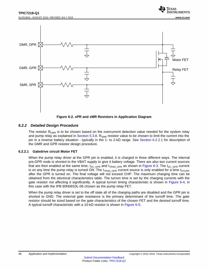
Motor FET
Relay FET
DMR, DPR
GMR, GPR
SMR, SPR
TPIC7218-Q1SLDS182A –AUGUST 2010–REVISED JULY 2015 www.ti.com
Figure 6-2. xPR and xMR Resistors in Application Diagram
6.2.2 Detailed Design ProcedureThe resistor RDMR is to be chosen based on the overcurrent detection value needed for the system relayand pump relay as explained in Section 5.3.8. RSMR resistor value to be chosen to limit the current into thepin in a reverse battery situation - typically in the 1- to 2-kΩ range. See Section 6.2.2.1 for description ofthe GMR and GPR resistor design procedure.
6.2.2.1 Gatedrive circuit Motor FET
When the pump relay driver at the GPR pin is enabled, it is charged in three different ways. The internalpre-GPR node is shorted to the VBAT supply to give it battery voltage. There are also two current sourcesthat are then enabled at the same time, IDC_GPR and ITRAN_GPR as shown in Figure 6-3. The IDC_GPR currentis on any time the pump relay is turned ON. The ITRAN_GPR current source is only enabled for a time tSTGPRafter the GPR is turned on. The final voltage will not exceed CHP. The maximum charging time can beobtained from the electrical characteristics table. The turnon time is set by the charging currents with thegate resistor not affecting it significantly. A typical turnon timing characteristic is shown in Figure 6-4, inthis case with the IPB 80N06S3L-06 chosen as the pump relay FET.
When the pump relay driver is set to the off state all of the charging paths are disabled and the GPR pin isshorted to GND. The external gate resistance is the primary determinant of the turnoff time. The gateresistor should be sized based on the gate characteristics of the chosen FET and the desired turnoff time.A typical turnoff characteristic with a 10-kΩ resistor is shown in Figure 6-5.
48 Application and Implementation Copyright © 2010–2015, Texas Instruments IncorporatedSubmit Documentation Feedback
Product Folder Links: TPIC7218-Q1

MOTOR GND
V_ BAT
V _ BAT
CCHP
GPR
150k
2 .5k70 u
GATE DRIVE
Enable
Enable
Disable
CPC
VBATHSPC
GE_motorFET
SPI
ITRAN _GPR
IDC_GPR
TPIC7218-Q1www.ti.com SLDS182A –AUGUST 2010–REVISED JULY 2015
Figure 6-3. Pump Relay Gatedriver Circuit
6.2.2.2 Gatedrive circuit Master Relay FET
The circuit used for the gate drive for the master relay FET is similar to the pump motor FET gatedrivewith changes in the drive strength as reflected in the turnon times from the electrical characteristics table.The gate resistor for the master relay FET should be chosen using the same procedure as for the pumpmotor relay driver.
6.2.3 Application Curves
Figure 6-4. Turnon of the FET Gate With a 10-kΩ Gate Resistor. Figure 6-5. Turnon of the FET Gate With a 10-kΩ Gate Resistor.
Copyright © 2010–2015, Texas Instruments Incorporated Application and Implementation 49Submit Documentation Feedback
Product Folder Links: TPIC7218-Q1

TPIC7218-Q1SLDS182A –AUGUST 2010–REVISED JULY 2015 www.ti.com
7 Power Supply Recommendations
The TPIC7218-Q1 device requires three power supply input pins – (1) VBAT connected to the automotivebattery, (2) VDD connected to a 5-V regulated output from the battery and (3) VIO which can be optionallyconnected to VDD or a 3.3-V regulated output. TI recommends that all power supply pins have decouplingcapacitors. Use good circuit board layout techniques to ensure each capacitor provides instantaneouspeak current to the TPIC7218-Q1 device. Care must be taken to avoid parasitic impedances which candegrade decoupling performance. Poorly decoupled power pins are likely to cause unsatisfactory EMCperformance. TI recommends the following capacitor values:• VBAT: recommended, 0.1 µF, X7R, 10%• VDD: recommended, 0.1 µF, X7R, 10%• VCC3: required, 100 pF, X7R, 10%
8 Layout
8.1 Layout Guidelines
8.1.1 Local Grounding Configuration
Route the ground pins 6, 24, 29, 30, 31, 32, 37, 63, 64, 69, 70, 71, 72 and 77 directly inward to pad.Maximize plane area under the TPIC7218-Q1 device to be consistent with PCB design rules. Ensureproper relief features for soldering thermal pad to plated through holes.
Add additional plated through holes as shown in the sketch to minimize loop area for ground returncurrents. See Figure 8-1 for more information.
8.1.2 Board Level Grounding Configuration, TPIC7218-Q1 to System ConnectorIdeally the inner PCB layer under the TPIC7218-Q1 device should be dedicated as plane ground, withdirect connection to wiring connector pin to vehicle ground. The layer should cover entire PCB area, withonly clearance holes for vias and so forth. No breaks or divisions. See Figure 8-2 for more information.
8.1.3 VCC3 Bypass Capacitor
Place 0402 package bypass capacitor for VCC3 node to ground as close as possible to the TPIC7218-Q1device, absolute minimum loop width and trace length. Do not connect ground side of capacitor to anyplane; tie it directly with top layer trace to pin 6 as shown in Figure 8-3. Close placement, minimum looparea is a priority.
8.1.4 VDD Bypass Capacitor
VDD bypass capacitor needs to be close to the TPIC7218-Q1 device, but not as critical as VCC3 cap. Theorientation and location shown in Figure 8-4 is just an example. Connection between capacitor and groundnode to be made through a through to the inner ground plane layer.
8.1.5 VBAT and CHP Capacitors
Three capacitors are used for bypassing the VBAT node. Prioritize placing an 0402 as close as possible topin 59. The other two need to be close but not as critical. Ground capacitors. Capacitor ground needs tobe connected to inner plane. The 0805 package is suitable for the other two capacitors.
Two capacitors are used between pin 59 and 60, and as with VBAT node, the 0402 capacitor needs to beas close as possible to the TPIC7218-Q1 device. The 0805 package is suitable for the other capacitor.See Figure 8-5 for more information.
50 Layout Copyright © 2010–2015, Texas Instruments IncorporatedSubmit Documentation Feedback
Product Folder Links: TPIC7218-Q1

TPIC7218-Q1www.ti.com SLDS182A –AUGUST 2010–REVISED JULY 2015
8.1.6 Multiple Plane Layer AssignmentsPlace components associated with VCC3 (pin 3), VDD (pin 9), VBAT (pin 59), CHP (pin 60), DMR (pin55), SMR (pin 56), GMR (pin 57), GPR (pin 58), SPR (pin 61) and DPR (pin 62) on top layer. Assign firstPCB layer under the top layer as an overall ground plane.
Placing components on top-side of board and assigning first inner layer as ground plane minimizes thepath length and loop area for EMC bypassing. See Figure 8-6 for more information.
8.1.7 Duplicate Pad Under TPIC7218-Q1 on All Non-Ground Plane Inner Layers
Duplicate the top layer pad underneath the TPIC7218-Q1 device on all of the inner layers. For the firstinner ground plane layer, entire plane is ground except for clearances around holes and unconnectedvias. Bottom layer copper pad directly under the TPIC7218-Q1 device is sized and has relief features asrequired for the thermal slug. See Figure 8-6 for more information.
8.1.8 FloodingFlooding places copper on all available area, subject to the clearance rules for the manufacture of thePCB. Flooded areas should be connected by vias to the inner ground plane layer. Small, insignificantflooded zones may be left unconnected or deleted from the design.
The additional copper connected to ground augments the effectiveness of the inner ground plane layer byproviding parallel paths, and also improves heat sink performance by increasing the thermal mass of thePCB. See Figure 8-7 for more information.
Copyright © 2010–2015, Texas Instruments Incorporated Layout 51Submit Documentation Feedback
Product Folder Links: TPIC7218-Q1

PCB
TPIC7218
System Connector
Pin 6,GND
80 79 78 76 75 74 73 68 67 66 65 62 61
1 60
2 59
3 58
4 57
5 56
55
7 54
8 53
9 52
10 51
11 50
12 49
13 48
14 47
15 46
16 45
17 44
18 43
19 42
20 41 21 22 23 25 26 27 28 33 34 35 36 38 39 40
Pin
77,
PG
ND
8
Pin
72,
PG
ND
7
Pin
71,
PG
ND
7
Pin
70,
PG
ND
6
Pin
69,
PG
ND
6
Pin
64,
PG
ND
5
Pin
63,
PG
ND
5
Pin
37,
PG
ND
1
Pin
32,
PG
ND
2
Pin
31,
PG
ND
2
Pin
30,
PG
ND
3
Pin
29,
PG
ND
3
Pin
24,
PG
ND
4
TPIC7218-Q1SLDS182A –AUGUST 2010–REVISED JULY 2015 www.ti.com
8.2 Layout Example
Figure 8-1. Local Grounding Configuration Layout Example
Figure 8-2. Board Level Grounding Configuration, TPIC7218-Q1 to System Connector Layout Example
52 Layout Copyright © 2010–2015, Texas Instruments IncorporatedSubmit Documentation Feedback
Product Folder Links: TPIC7218-Q1

Pin 6,GND
80 79 78 76 75 74 73 68 67 66 65 62 61
1 60
2 59
3 58
4 57
5 56
55
54
8 53
9 52
10 51
11 50
12 49
13 48
14 47
15 46
16 45
17 44
18 43
19 42
20 41 21 22 23 25 26 27 28 33 34 35 36 38 39 40
Pin
77,
PG
ND
8
Pin
72,
PG
ND
7
Pin
71,
PG
ND
7
Pin
70,
PG
ND
6
Pin
69,
PG
ND
6
Pin
64,
PG
ND
5
Pin
63,
PG
ND
5
Pin
37,
PG
ND
1
Pin
32,
PG
ND
2
Pin
31,
PG
ND
2
Pin
30,
PG
ND
3
Pin
29,
PG
ND
3
Pin
24,
PG
ND
4
Pin 7,VCC3
Minimize Trace Loop Area
TPIC7218-Q1www.ti.com SLDS182A –AUGUST 2010–REVISED JULY 2015
Figure 8-3. VCC3 Bypass Capacitor Layout Example
Copyright © 2010–2015, Texas Instruments Incorporated Layout 53Submit Documentation Feedback
Product Folder Links: TPIC7218-Q1

Pin 6,GND
80 79 78 76 75 74 73 68 67 66 65 62 61
1 60
2 59
3 58
4 57
5 56
55
54
8 53
52
10 51
11 50
12 49
13 48
14 47
15 46
16 45
17 44
18 43
19 42
20 41 21 22 23 25 26 27 28 33 34 35 36 38 39 40
Pin
77,
PG
ND
8
Pin
72,
PG
ND
7
Pin
71,
PG
ND
7
Pin
70,
PG
ND
6
Pin
69,
PG
ND
6
Pin
64,
PG
ND
5
Pin
63,
PG
ND
5
Pin
37,
PG
ND
1
Pin
32,
PG
ND
2
Pin
31,
PG
ND
2
Pin
30,
PG
ND
3
Pin
29,
PG
ND
3
Pin
24,
PG
ND
4
Pin 7,VCC3
Ground connection by via to inner plane
Pin 9,VDD
TPIC7218-Q1SLDS182A –AUGUST 2010–REVISED JULY 2015 www.ti.com
Figure 8-4. VDD Bypass Capacitor Layout Example
54 Layout Copyright © 2010–2015, Texas Instruments IncorporatedSubmit Documentation Feedback
Product Folder Links: TPIC7218-Q1

TPIC7218 Top
Inner layer 1 ground planeInner layer 2Inner layer 3Inner layer 4Inner layer 5
Bottom
Thermal Slug
Note short path back to ground
Pin 6,GND
80 79 78 76 75 74 73 68 67 66 65 62 61
1
2
3 58
4 57
5 56
55
54
8 53
9 52
10 51
11 50
12 49
13 48
14 47
15 46
16 45
17 44
18 43
19 42
20 41 21 22 23 25 26 27 28 33 34 35 36 38 39 40
Pin
77,
PG
ND
8
Pin
72,
PG
ND
7
Pin
71,
PG
ND
7
Pin
70,
PG
ND
6
Pin
69,
PG
ND
6
Pin
64,
PG
ND
5
Pin
63,
PG
ND
5
Pin
37,
PG
ND
1
Pin
32,
PG
ND
2
Pin
31,
PG
ND
2
Pin
30,
PG
ND
3
Pin
29,
PG
ND
3
Pin
24,
PG
ND
4
Pin 59,VBAT
Ground connection by via to inner plane
70402 capacitors as close as
possible
Pin 60,CHP
TPIC7218-Q1www.ti.com SLDS182A –AUGUST 2010–REVISED JULY 2015
Figure 8-5. VBAT and CHP Capacitors Layout Example
Figure 8-6. Multiple Plane Layer Assignments Layout Example
Copyright © 2010–2015, Texas Instruments Incorporated Layout 55Submit Documentation Feedback
Product Folder Links: TPIC7218-Q1

TPIC7218 Top
Inner layer 1 ground planeInner layer 2Inner layer 3Inner layer 4Inner layer 5
Bottom
Thermal Slug
TPIC7218-Q1SLDS182A –AUGUST 2010–REVISED JULY 2015 www.ti.com
Figure 8-7. Thermal Slug Layout Example
9 Device and Documentation Support
9.1 Documentation Support
9.1.1 Related DocumentationFor related documentation see the following: TPIC7218-Q1 Thermal Design Considerations and Solution,SLDA013
9.2 Community ResourcesThe following links connect to TI community resources. Linked contents are provided "AS IS" by therespective contributors. They do not constitute TI specifications and do not necessarily reflect TI's views;see TI's Terms of Use.
TI E2E™ Online Community TI's Engineer-to-Engineer (E2E) Community. Created to fostercollaboration among engineers. At e2e.ti.com, you can ask questions, share knowledge,explore ideas and help solve problems with fellow engineers.
Design Support TI's Design Support Quickly find helpful E2E forums along with design support toolsand contact information for technical support.
9.3 TrademarksPowerPAD, E2E are trademarks of Texas Instruments.All other trademarks are the property of their respective owners.
56 Device and Documentation Support Copyright © 2010–2015, Texas Instruments IncorporatedSubmit Documentation Feedback
Product Folder Links: TPIC7218-Q1

TPIC7218-Q1www.ti.com SLDS182A –AUGUST 2010–REVISED JULY 2015
9.4 Electrostatic Discharge CautionThese devices have limited built-in ESD protection. The leads should be shorted together or the device placed in conductive foamduring storage or handling to prevent electrostatic damage to the MOS gates.
9.5 GlossarySLYZ022 — TI Glossary.
This glossary lists and explains terms, acronyms, and definitions.
10 Mechanical, Packaging, and Orderable Information
The following pages include mechanical, packaging, and orderable information. This information is themost current data available for the designated devices. This data is subject to change without notice andrevision of this document. For browser-based versions of this data sheet, refer to the left-hand navigation.
Copyright © 2010–2015, Texas Instruments Incorporated Mechanical, Packaging, and Orderable Information 57Submit Documentation Feedback
Product Folder Links: TPIC7218-Q1

PACKAGE OPTION ADDENDUM
www.ti.com 12-Oct-2014
Addendum-Page 1
PACKAGING INFORMATION
Orderable Device Status(1)
Package Type PackageDrawing
Pins PackageQty
Eco Plan(2)
Lead/Ball Finish(6)
MSL Peak Temp(3)
Op Temp (°C) Device Marking(4/5)
Samples
TPIC7218QPFPRQ1 ACTIVE HTQFP PFP 80 1000 Green (RoHS& no Sb/Br)
CU NIPDAU Level-3-260C-168 HR -40 to 125 TPIC7218Q
(1) The marketing status values are defined as follows:ACTIVE: Product device recommended for new designs.LIFEBUY: TI has announced that the device will be discontinued, and a lifetime-buy period is in effect.NRND: Not recommended for new designs. Device is in production to support existing customers, but TI does not recommend using this part in a new design.PREVIEW: Device has been announced but is not in production. Samples may or may not be available.OBSOLETE: TI has discontinued the production of the device.
(2) Eco Plan - The planned eco-friendly classification: Pb-Free (RoHS), Pb-Free (RoHS Exempt), or Green (RoHS & no Sb/Br) - please check http://www.ti.com/productcontent for the latest availabilityinformation and additional product content details.TBD: The Pb-Free/Green conversion plan has not been defined.Pb-Free (RoHS): TI's terms "Lead-Free" or "Pb-Free" mean semiconductor products that are compatible with the current RoHS requirements for all 6 substances, including the requirement thatlead not exceed 0.1% by weight in homogeneous materials. Where designed to be soldered at high temperatures, TI Pb-Free products are suitable for use in specified lead-free processes.Pb-Free (RoHS Exempt): This component has a RoHS exemption for either 1) lead-based flip-chip solder bumps used between the die and package, or 2) lead-based die adhesive used betweenthe die and leadframe. The component is otherwise considered Pb-Free (RoHS compatible) as defined above.Green (RoHS & no Sb/Br): TI defines "Green" to mean Pb-Free (RoHS compatible), and free of Bromine (Br) and Antimony (Sb) based flame retardants (Br or Sb do not exceed 0.1% by weightin homogeneous material)
(3) MSL, Peak Temp. - The Moisture Sensitivity Level rating according to the JEDEC industry standard classifications, and peak solder temperature.
(4) There may be additional marking, which relates to the logo, the lot trace code information, or the environmental category on the device.
(5) Multiple Device Markings will be inside parentheses. Only one Device Marking contained in parentheses and separated by a "~" will appear on a device. If a line is indented then it is a continuationof the previous line and the two combined represent the entire Device Marking for that device.
(6) Lead/Ball Finish - Orderable Devices may have multiple material finish options. Finish options are separated by a vertical ruled line. Lead/Ball Finish values may wrap to two lines if the finishvalue exceeds the maximum column width.
Important Information and Disclaimer:The information provided on this page represents TI's knowledge and belief as of the date that it is provided. TI bases its knowledge and belief on informationprovided by third parties, and makes no representation or warranty as to the accuracy of such information. Efforts are underway to better integrate information from third parties. TI has taken andcontinues to take reasonable steps to provide representative and accurate information but may not have conducted destructive testing or chemical analysis on incoming materials and chemicals.TI and TI suppliers consider certain information to be proprietary, and thus CAS numbers and other limited information may not be available for release.
In no event shall TI's liability arising out of such information exceed the total purchase price of the TI part(s) at issue in this document sold by TI to Customer on an annual basis.

PACKAGE OPTION ADDENDUM
www.ti.com 12-Oct-2014
Addendum-Page 2

TAPE AND REEL INFORMATION
*All dimensions are nominal
Device PackageType
PackageDrawing
Pins SPQ ReelDiameter
(mm)
ReelWidth
W1 (mm)
A0(mm)
B0(mm)
K0(mm)
P1(mm)
W(mm)
Pin1Quadrant
TPIC7218QPFPRQ1 HTQFP PFP 80 1000 330.0 24.4 15.0 15.0 1.5 20.0 24.0 Q2
PACKAGE MATERIALS INFORMATION
www.ti.com 13-Oct-2014
Pack Materials-Page 1

*All dimensions are nominal
Device Package Type Package Drawing Pins SPQ Length (mm) Width (mm) Height (mm)
TPIC7218QPFPRQ1 HTQFP PFP 80 1000 367.0 367.0 45.0
PACKAGE MATERIALS INFORMATION
www.ti.com 13-Oct-2014
Pack Materials-Page 2


IMPORTANT NOTICE
Texas Instruments Incorporated and its subsidiaries (TI) reserve the right to make corrections, enhancements, improvements and otherchanges to its semiconductor products and services per JESD46, latest issue, and to discontinue any product or service per JESD48, latestissue. Buyers should obtain the latest relevant information before placing orders and should verify that such information is current andcomplete. All semiconductor products (also referred to herein as “components”) are sold subject to TI’s terms and conditions of salesupplied at the time of order acknowledgment.TI warrants performance of its components to the specifications applicable at the time of sale, in accordance with the warranty in TI’s termsand conditions of sale of semiconductor products. Testing and other quality control techniques are used to the extent TI deems necessaryto support this warranty. Except where mandated by applicable law, testing of all parameters of each component is not necessarilyperformed.TI assumes no liability for applications assistance or the design of Buyers’ products. Buyers are responsible for their products andapplications using TI components. To minimize the risks associated with Buyers’ products and applications, Buyers should provideadequate design and operating safeguards.TI does not warrant or represent that any license, either express or implied, is granted under any patent right, copyright, mask work right, orother intellectual property right relating to any combination, machine, or process in which TI components or services are used. Informationpublished by TI regarding third-party products or services does not constitute a license to use such products or services or a warranty orendorsement thereof. Use of such information may require a license from a third party under the patents or other intellectual property of thethird party, or a license from TI under the patents or other intellectual property of TI.Reproduction of significant portions of TI information in TI data books or data sheets is permissible only if reproduction is without alterationand is accompanied by all associated warranties, conditions, limitations, and notices. TI is not responsible or liable for such altereddocumentation. Information of third parties may be subject to additional restrictions.Resale of TI components or services with statements different from or beyond the parameters stated by TI for that component or servicevoids all express and any implied warranties for the associated TI component or service and is an unfair and deceptive business practice.TI is not responsible or liable for any such statements.Buyer acknowledges and agrees that it is solely responsible for compliance with all legal, regulatory and safety-related requirementsconcerning its products, and any use of TI components in its applications, notwithstanding any applications-related information or supportthat may be provided by TI. Buyer represents and agrees that it has all the necessary expertise to create and implement safeguards whichanticipate dangerous consequences of failures, monitor failures and their consequences, lessen the likelihood of failures that might causeharm and take appropriate remedial actions. Buyer will fully indemnify TI and its representatives against any damages arising out of the useof any TI components in safety-critical applications.In some cases, TI components may be promoted specifically to facilitate safety-related applications. With such components, TI’s goal is tohelp enable customers to design and create their own end-product solutions that meet applicable functional safety standards andrequirements. Nonetheless, such components are subject to these terms.No TI components are authorized for use in FDA Class III (or similar life-critical medical equipment) unless authorized officers of the partieshave executed a special agreement specifically governing such use.Only those TI components which TI has specifically designated as military grade or “enhanced plastic” are designed and intended for use inmilitary/aerospace applications or environments. Buyer acknowledges and agrees that any military or aerospace use of TI componentswhich have not been so designated is solely at the Buyer's risk, and that Buyer is solely responsible for compliance with all legal andregulatory requirements in connection with such use.TI has specifically designated certain components as meeting ISO/TS16949 requirements, mainly for automotive use. In any case of use ofnon-designated products, TI will not be responsible for any failure to meet ISO/TS16949.
Products ApplicationsAudio www.ti.com/audio Automotive and Transportation www.ti.com/automotiveAmplifiers amplifier.ti.com Communications and Telecom www.ti.com/communicationsData Converters dataconverter.ti.com Computers and Peripherals www.ti.com/computersDLP® Products www.dlp.com Consumer Electronics www.ti.com/consumer-appsDSP dsp.ti.com Energy and Lighting www.ti.com/energyClocks and Timers www.ti.com/clocks Industrial www.ti.com/industrialInterface interface.ti.com Medical www.ti.com/medicalLogic logic.ti.com Security www.ti.com/securityPower Mgmt power.ti.com Space, Avionics and Defense www.ti.com/space-avionics-defenseMicrocontrollers microcontroller.ti.com Video and Imaging www.ti.com/videoRFID www.ti-rfid.comOMAP Applications Processors www.ti.com/omap TI E2E Community e2e.ti.comWireless Connectivity www.ti.com/wirelessconnectivity
Mailing Address: Texas Instruments, Post Office Box 655303, Dallas, Texas 75265Copyright © 2016, Texas Instruments Incorporated