TOSHIBA PHOTOCOUPLER GaA TLP104
13
TLP104 2014-09-01 1 TOSHIBA PHOTOCOUPLER GaAℓAs LED & PHOTO-IC TLP104 IPM (Intelligent Power Module) Industrial Inverter Operate at high ambient temperatures up to 125°C The Toshiba TLP104 consists of GaAℓAs infrared light emitting diodes and integrated high gain, high-speed photodetectors. The TLP104 is housed in the SO6 package. The output stage is an open collector type. The photodetector has an internal Faraday shield that provides a guaranteed common-mode transient immunity of ±15 kV/μs. TLP104 guarantees minimum and maximum of propagation delay time, switching speed dispersion, and high common mode transient immunity. Therefore TLP104 is suitable for isolation interface between IPM (Intelligent Power Module) in motor control application. Inverter logic type (Open collector output) Package type: SO6 Guaranteed performance over temperature: -40 to 125℃ Power supply voltage: -0.5 to 30 V Threshold Input Current: I FHL = 5.0 mA (max) Propagation delay time (t pHL /t pLH ): t pHL = 400ns (max) t pLH = 550ns (max) Switching Time Dispersion(|t pHL -t pLH |): 400ns (max) Common mode transient immunity : ±15kV/μs (min) Isolation voltage : 3750Vrms (min) UL approved : UL1577, File No.E67349 c-UL approved :CSA Component Acceptance Service No. 5A, File No.E67349 Truth Table Input LED Output H ON L L OFF H JEDEC ― JEITA ― TOSHIBA 11-4L1 Weight: 0.08 g(typ.) Creepage distance 5.0 mm (min) Clearance distance 5.0 mm (min) Insulation thickness 0.4 mm (min) Unit: mm 0.1 2.1 ± 0.1 4.55 1 3 6 5 4 3.7 7.0 ± 0.4 0.4 2.54 1.27 0.5 min 0.15 +0.25 -0.15 +0.25 -0.15 V CC GND I CC 6 4 SHIELD 3- 1+ IF IO IO V O 5 1:ANODE 3:CATHODE 4:GND 5:V O (Output) 6:V CC V CC GND SHIELD 1 3 4 5 6 Pin Configuration (Top View) Schematic Construction Mechanical Ratings Start of commercial production 2009/10
Transcript of TOSHIBA PHOTOCOUPLER GaA TLP104

TLP104
2014-09-01 1
TOSHIBA PHOTOCOUPLER GaAℓAs LED & PHOTO-IC
TLP104
IPM (Intelligent Power Module) Industrial Inverter Operate at high ambient temperatures up to 125°C
The Toshiba TLP104 consists of GaAℓAs infrared light emitting diodes and integrated high gain, high-speed photodetectors. The TLP104 is housed in the SO6 package. The output stage is an open collector type.
The photodetector has an internal Faraday shield that provides a guaranteed common-mode transient immunity of ±15 kV/μs. TLP104 guarantees minimum and maximum of propagation delay time, switching speed dispersion, and high common mode transient immunity. Therefore TLP104 is suitable for isolation interface between IPM (Intelligent Power Module) in motor control application.
Inverter logic type (Open collector output)
Package type: SO6
Guaranteed performance over temperature: -40 to 125
Power supply voltage: -0.5 to 30 V
Threshold Input Current: IFHL = 5.0 mA (max)
Propagation delay time (tpHL/tpLH): tpHL = 400ns (max)
tpLH = 550ns (max)
Switching Time Dispersion(|tpHL-tpLH|): 400ns (max)
Common mode transient immunity : ±15kV/μs (min)
Isolation voltage : 3750Vrms (min)
UL approved : UL1577, File No.E67349
c-UL approved :CSA Component Acceptance Service
No. 5A, File No.E67349
Truth Table
Input LED Output
H ON L
L OFF H
JEDEC ―
JEITA ―
TOSHIBA 11-4L1
Weight: 0.08 g(typ.)
Creepage distance 5.0 mm (min)
Clearance distance 5.0 mm (min)
Insulation thickness 0.4 mm (min)
Unit: mm
0.1
2
.1 ±
0.1
4.55
1 3
6 5 4
3.7 7.0 ± 0.4
0.4
2.54
1.27
0.5 min
0.1
5
+0
.25
-0
.15
+0.25 -0.15
VCC
GND
ICC
6
4SHIELD
3-
1+
IF
IO IO
VO
5
1:ANODE 3:CATHODE 4:GND 5:VO(Output) 6:VCC
VCC
GND SHIELD
1
3 4
5
6
Pin Configuration (Top View)
Schematic
Construction Mechanical Ratings
Start of commercial production2009/10

TLP104
2014-09-01 2
Absolute Maximum Ratings (Ta = 25°C)
Characteristic Symbol Rating Unit
LED
Forward Current IF 25 mA
Forward Current Derating (Ta ≥ 110°C) ∆IF /°C -0.67 mA/°C
Pulse Forward Current (Note 1) IFP 50 mA
Pulse Forward Current Derating (Ta ≥ 110°C) ∆IFP /°C -1.34 mA/°C
Reverse Voltage VR 5 V
Det
ecto
r
Output Current (Ta ≤ 125) IO 8 mA
Output Voltage VO -0.5 to 30 V
Supply Voltage VCC -0.5 to 30 V
Output Power Dissipation PO 80 mW
Output Power Dissipation Derating (Ta ≥ 110°C) ∆PO /°C -2.0 mW/°C
Operating Temperature Range Topr -40 to 125 °C
Storage Temperature Range Tstg -55 to 125 °C
Lead Soldering Temperature (10 s) Tsol 260 °C
Isolation Voltage (AC,1 minute, R.H.≤ 60%,Ta=25°C) (Note 2) BVs 3750 Vrms
Note: Using continuously under heavy loads (e.g. the application of high temperature/current/voltage and the significant change in temperature, etc.) may cause this product to decrease in the reliability significantly even if the operating conditions (i.e. operating temperature/current/voltage, etc.) are within the absolute maximum ratings. Please design the appropriate reliability upon reviewing the Toshiba Semiconductor Reliability Handbook (“Handling Precautions”/“Derating Concept and Methods”) and individual reliability data (i.e. reliability test report and estimated failure rate, etc).
Note 1: Pulse width ≤ 10μs, duty=10%.
Note 2: This device is regarded as a two terminal device: pins 1 and 3 are shorted together, as are pins 4, 5 and 6.
Recommended Operating Conditions
Characteristic Symbol Min Typ. Max Unit
Input Current , High Level IFHL 7.5 - 15 mA
Input Voltage , Low Level VFLH 0 - 0.8 V
Supply Voltage* VCC 4.5 - 30 V
Operating Temperature Topr -40 - 125 °C
* This item denotes operating range, not meaning of recommended operating conditions. Note: Recommended operating conditions are given as a design guideline to obtain expected performance of the
device. Additionally, each item is an independent guideline respectively. In developing designs using this product, please confirm specified characteristics shown in this document.

TLP104
2014-09-01 3
Electrical Characteristics (Unless otherwise specified, Ta = −40 to 125°C, VCC =4.5 to 30V)
Characteristic Symbol Test
CircuitTest Condition Min Typ. Max Unit
LED
Forward voltage VF ⎯ IF = 10 mA, Ta=25°C 1.45 1.61 1.85 V
Forward voltage temperature coefficient
∆VF / ∆Ta ⎯ IF = 10 mA ― -1.8 ― mV /°C
Reverse current IR ⎯ VR = 5 V, Ta=25°C ― ― 10 μA
Capacitance between terminals
CT ⎯ V = 0V, f = 1 MHz ― 60 ― pF
Det
ecto
r
High level output current IOH 1 VF = 0.8 V, VO < VCC ― ― 50 μA
Low level output voltage VOL 2 IF = 10 mA, IO = 2.4mA ― 0.2 0.6 V
Low level supply current ICCL 3 IF = 10 mA ― ― 1.3 mA
High level supply current ICCH 4 IF = 0 mA ― ― 1.3 mA
Output current IO ⎯ IF = 10 mA, VO = 0.6V 4.0 ― ― mA
Input current logic LOW output IFHL ⎯ IO = 0.75mA, VO < 0.8 V ― 1.0 5 mA
Input voltage logic HIGH output VFLH ⎯ IO = 0.75mA, VO > 2.0 V 0.8 ― ― V
*All typical values are at Ta=25°C, VCC=5 V unless otherwise specified
Isolation Characteristics (Ta = 25°C)
Characteristic Symbol Test Conditions Min Typ. Max Unit
Capacitance input to output CS VS = 0V, f = 1 MHz (Note 2) ― 0.8 ― pF
Isolation resistance RS R.H. ≤ 60%, VS = 500 V (Note 2) 1×10¹² 10
14 ― Ω
Isolation voltage BVS
AC,1 minute 3750 ― ― Vrms
AC,1 second, in oil ― 10000 ―
DC,1 minute, in oil ― 10000 ― Vdc

TLP104
2014-09-01 4
Switching Characteristics (Unless otherwise specified, Ta = −40 to 125°C, VCC=15V)
Characteristic Symbol Test
CircuitTest Condition Min Typ. Max Unit
Propagation delay time (H→L) tpHL
5 IF = 10 mA,
RL = 20kΩ
(Note 4)
CL=100pF 30 150 400
ns
CL=10pF ― 90 ―
Propagation delay time (L→H) tpLH CL=100pF 150 350 550
CL=10pF ― 100 ―
Switching Time Dispersion
between ON and OFF |tpHL−tpLH|
CL=100pF
― ― 400
Propagation Delay Skew tpLH−tpHL -50 ― 450
Common mode transient immunity
at high output level CMH
6
VCM = 1500 Vp−p, IF = 0 mA RL = 20 kΩ, Ta=25°C
15 ― ― kV/μs
Common mode transient Immunity
at low output level CML
VCM = 1500 Vp−p, IF = 10 mA RL = 20 kΩ, Ta=25°C
−15 ― ― kV/μs
*All typical values are at Ta=25°C
Note 3: A ceramic capacitor (0.1 μF) should be connected from pin 6 (VCC) to pin 4 (GND) to stabilize the operation of
the high gain linear amplifier. Failure to provide the bypass may impair the switching property.
The total lead length between capacitor and coupler should not exceed 1 cm.
Note 4: f = 10kHz, duty=10%, input current tr = tf = 5ns
Note 5: Propagation delay skew is defined as the propagation delay time of the largest or smallest tpLH minus
the largest or smallest tpHL of multiple samples. Evaluations of these samples are conducted under identical
test conditions (supply voltage, input current, temperature, etc.).
TEST CIRCUIT 1: IOH TEST CIRCUIT 2: VOL
TEST CIRCUIT 3: ICCL TEST CIRCUIT 4: ICCH
IF
A
VCC0.1 μF
ICCL
0.1μF
VOL VCC V
IO↑
SHIELD
IF
SHIELD
A
VCC0.1 μF
ICCH
SHIELD
0.1μF
SHIELD
VF
VCC
IOH
A
VO
TLP104
2014-09-01 5
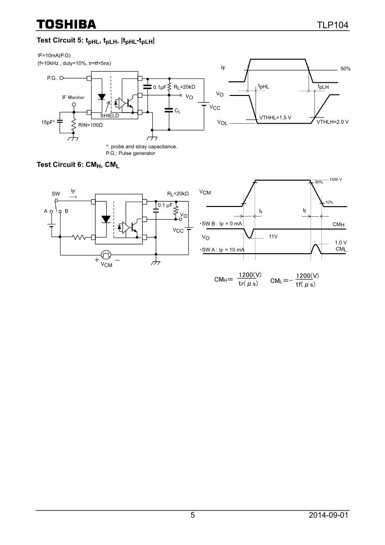
Test Circuit 5: tpHL, tpLH, |tpHL-tpLH| Test Circuit 6: CMH, CML
VO
VOL
tpLH tpHL
VTHHL=1.5 V
50%IF
0.1μF
RIN=100Ω 15pF*
CL
RL=20kΩ
IF=10mA(P.G)
(f=10kHz , duty=10%, tr=tf=5ns)
IF Monitor VO
P.G.
SHIELD
VCC
VTHLH=2.0 V
VCM
10%
90% 1500 V
・SW B : IF = 0 mA
・SW A : IF = 10 mA 1.0 V
11V VO
tr tf
CML
CMH
+ -
SW
B
VCC
VCM
VO
0.1 μF
IF
A
RL=20kΩ→
CMH=1200(V)
tr(μs) CML=-1200(V)
tf(μs)
*: probe and stray capacitance. P.G.: Pulse generator

TLP104
2014-09-01 6
I F - V F
I F H L - T a
Inp
ut
forw
ard
cu
rre
nt
I F (
mA
)
Inp
ut
cu
rre
nt
log
ic L
OW
ou
tpu
t
I F
HL
(mA
)
I npu t fo rward vo l tage V F (V) Ambient tempera tu re Ta ()
I C C L - T a I C C H - T a
L
ow
le
ve
l s
up
ply
cu
rre
nt
I CC
L (m
A)
Hig
h l
ev
el
su
pp
ly c
urr
en
t I C
CH
(m
A)
Ambient tempera tu re Ta () Ambient tempera tu re Ta ()
V O L - T a I O H - T a
Lo
w l
ev
el
ou
tpu
t v
olt
ag
e
VO
L (V
)
Hig
h l
ev
el
ou
tpu
t c
urr
en
t I O
H (μ
A)
Ambient tempera tu re Ta () Ambient tempera tu re Ta ()
*: The above graphs show typical characteristics.
0.1
1
10
100
1 1.2 1.4 1.6 1.8 2 2.20
1
2
3
4
5
-40 -20 0 20 40 60 80 100 120 140
0
0.2
0.4
0.6
0.8
1
1.2
1.4
-40 -20 0 20 40 60 80 100 120 140
0
0.2
0.4
0.6
0.8
1
1.2
1.4
-40 -20 0 20 40 60 80 100 120 140
0
0.1
0.2
0.3
0.4
0.5
0.6
-40 -20 0 20 40 60 80 100 120 1400
0.4
0.8
1.2
1.6
2
-40 -20 0 20 40 60 80 100 120 140
Vcc = 30 V
Vcc = 15 V Io = 0.75 mA Vo < 0.8 V
Vcc = 30 V IF = 10 mA
Ta=125˚C100˚C75˚C50˚C25˚C0˚C
-20˚C-40˚C
IF = 10 mA Vcc = 15 V Io = 2.4 mA
VF = 0.8 V Vcc = 30 V Vo = 30 V

TLP104
2014-09-01 7
t P H L / t P L H / | t P L H - t P H L | - C L t P H L / t P L H / | t P L H - t P H L | - Ta
Pro
paga
tion
dela
y tim
e、S
witc
hing
Tim
e D
ispe
rsio
n be
twe
en O
N a
nd O
FF
t
PH
L, t P
LH, |
t PLH
-tP
HL|
(ns
)
Pro
paga
tion
dela
y tim
e、S
witc
hing
Tim
e D
ispe
rsio
n be
twe
en O
N a
nd O
FF
t
PH
L, t P
LH, |
t PLH
-tP
HL|
(ns
)
Lord capac i tance CL (pF) Ambient temperature Ta ()
t P H L / t P L H / | t P L H - t P H L | - I F t P H L / t P L H / | t P L H - t P H L | - V C C
Pro
paga
tion
dela
y tim
e、
Sw
itchi
ng T
ime
Dis
pers
ion
betw
een
ON
and
OF
F
tP
HL,
t PLH
, |t P
LH-t
PH
L| (
ns)
Pro
paga
tion
dela
y tim
e、
Sw
itchi
ng T
ime
Dis
pers
ion
betw
een
ON
and
OF
F
tP
HL,
t PLH
, |t P
LH-t
PH
L| (
ns)
I npu t fo rward cu r ren t IF (mA) Supply voltage VCC (V)
t P H L / t P L H / | t P L H - t P H L | - R L
t P H L / t P L H / | t P L H - t P H L | - R L
Pro
paga
tion
dela
y tim
e、
Sw
itchi
ng T
ime
Dis
pers
ion
betw
een
ON
and
OF
F
tP
HL,
t PLH
, |t P
LH-t
PH
L| (
ns)
Pro
paga
tion
dela
y tim
e、
Sw
itchi
ng T
ime
Dis
pers
ion
betw
een
ON
and
OF
F
tP
HL,
t PLH
, |t P
LH-t
PH
L| (
ns)
Lord res i s tance RL (kΩ) Lord res i s tance RL (kΩ)
*: The above graphs show typical characteristics.
0
400
800
1200
1600
2000
0 100 200 300 400 500 600 700
0
100
200
300
400
500
-40 -20 0 20 40 60 80 100 120 140
0
100
200
300
400
500
0 5 10 15 20
-200
0
200
400
600
800
1000
1200
1400
0 5 10 15 20 25 30
0
200
400
600
800
1000
0 10 20 30 40 50
0
100
200
300
400
500
0 5 10 15 20
tPHL
IF = 10 mA, CL = 100 pF, RL = 20kΩ
Vcc = 15 V, CL = 100 pF, RL = 20kΩ
tPLH
|tPLH –tPHL|
tPLH
tPHL
|tPLH –tPHL|
IF = 10 mA, Vcc = 15 V CL = 100 pF
IF = 10 mA, Vcc = 5 V CL = 10 pF
|tPLH -tPHL|
tPHL
tPLH
|tPLH -tPHL|
tPHL
tPLH
IF = 10 mA, Vcc = 15 V CL = 100 pF, RL = 20kΩ
|tPLH –tPHL|
tPHL
tPLH
IF = 10 mA, Vcc = 15 V RL = 20kΩ
|tPLH -tPHL|
tPHL
tPLH

TLP104
2014-09-01 8
PRECAUTIONS OF SURFACE MOUNTING TYPE PHOTOCOUPLER SOLDERING & GENERAL STORAGE (1) Precautions for Soldering
1) When Using Soldering Reflow
An example of a temperature profile when Sn-Pb eutectic solder is used:
An example of a temperature profile when lead(Pb)-free solder is used:
Reflow soldering must be performed once or twice. The mounting should be completed with the interval from the first to the last mountings being 2 weeks.
2) When using soldering Flow (Applicable to both eutectic solder and Lead(Pb)-Free solder) Apply preheating of 150 for 60 to 120 seconds. Mounting condition of 260 or less within 10 seconds is recommended. Flow soldering must be performed once
3) When using soldering Iron (Applicable to both eutectic solder and Lead(Pb)-Free solder) Complete soldering within 10 seconds for lead temperature not exceeding 260 or within 3 seconds
not exceeding 350 . Heating by soldering iron must be only once per 1 lead
This profile is based on the device’s maximum heat resistance guaranteed value. Set the preheat temperature/heating temperature to the optimum temperature corresponding to the solder paste type used by the customer within the described profile.
This profile is based on the device’s maximum heat resistance guaranteed value. Set the preheat temperature/heating temperature to the optimum temperature corresponding to the solder paste type used by the customer within the described profile.
()
()

TLP104
2014-09-01 9
(2) Precautions for General Storage 1) Do not store devices at any place where they will be exposed to moisture or direct sunlight. 2) When transportation or storage of devices, follow the cautions indicated on the carton box. 3) The storage area temperature should be kept within a temperature range of 5
to 35 , and relative humidity should be maintained at between 45% and 75%. 4) Do not store devices in the presence of harmful (especially corrosive) gases, or in dusty conditions. 5) Use storage areas where there is minimal temperature fluctuation. Because rapid temperature
changes can cause condensation to occur on stored devices, resulting in lead oxidation or corrosion, as a result, the solderability of the leads will be degraded.
6) When repacking devices, use anti-static containers. 7) Do not apply any external force or load directly to devices while they are in storage. 8) If devices have been stored for more than two years, even though the above conditions have been
followed, it is recommended that solderability of them should be tested before they are used.

TLP104
2014-09-01 10
Specification for Embossed–Tape Packing (TPL)(TPR) for SO6 Coupler
1. Applicable Package
Package Product Type
SO6 Mini-flat coupler
2. Product Naming System Type of package used for shipment is denoted by a symbol suffix after a product number. The method of classification is as below.
(Example)
3. Tape Dimensions 3.1 Specification Classification Are as Shown in Table 1
Table 1 Tape Type Classification
Tape type Classification Quantity
(pcs / reel)
TPL L direction 3000
TPR R direction 3000
3.2 Orientation of Device in Relation to Direction of Tape Movement
Device orientation in the recesses is as shown in Figure 1.
Figure 1 Device Orientation
TLP104 (TPL)
Device name
Tape type
Direction of Tape
L direction R direction

TLP104
2014-09-01 11
3.3 Empty Device Recesses Are as Shown in Table 2.
Table 2 Empty Device Recesses
Standard Remarks
Occurrences of 2 or more successive empty device recesses
0 Within any given 40-mm section of tape, not including leader and trailer
Single empty device recesses
6 devices (max) per reel Not including leader and trailer
3.4 Start and End of Tape
The start of the tape has 50 or more empty holes. The end of tape has 50 or more empty holes and two empty turns only for a cover tape.
3.5 Tape Specification
(1) Tape material: Plastic (protection against electrostatics) (2) Dimensions: The tape dimensions are as shown in Figure 2 and Table 3.
Figure 2 Tape Forms
Table 3 Tape Dimensions
Unit: mm Unless otherwise specified: ±0.1
Symbol Dimension Remark
A 4.0 ―
B 7.6 ―
D 5.5 Center line of indented square hole and sprocket hole
E 1.75 Distance between tape edge and hole center
F 8.0 Cumulative error (max) per 10 feed holes
G 4.0 Cumulative error (max) per 10 feed holes
K0 2.6 Internal space
+0.1-0.3+0.1-0.3
0.3 ± 0.05
2.95 ± 0.2
K0
G
F
φ1.6 ± 0.1
A
E
D
B
12.0
± 0
.3
φ1.5 +0.1−0

TLP104
2014-09-01 12
3.6 Reel
(1) Material: Plastic (2) Dimensions: The reel dimensions are as shown in Figure 3 and Table 4.
Figure 3 Reel Form
Table 4 Reel Dimensions
Unit: mm
Symbol Dimension
A Φ380 ±2
B Φ80 ±1
C Φ13 ±0.5
E 2.0 ±0.5
U 4.0 ±0.5
W1 13.5 ±0.5
W2 17.5 ±1.0
4. Packing Either one reel or five reels of photocoupler are packed in a shipping carton.
5. Label Indication The carton bears a label indicating the product number, the symbol representing classification of standard, the quantity, the lot number and the Toshiba company name.
6. Ordering Method When placing an order, please specify the product number, the tape type and the quantity as shown in the following example.
(Example)
E
W1
W2
A
B
C U
TLP104 (TPL) 3000 pcs
Device name
Tape type
Quantity (must be a multiple of 3000)
TLP104
2014-09-01 13
RESTRICTIONS ON PRODUCT USE
• Toshiba Corporation, and its subsidiaries and affiliates (collectively "TOSHIBA"), reserve the right to make changes to the information in this document, and related hardware, software and systems (collectively "Product") without notice.
• This document and any information herein may not be reproduced without prior written permission from TOSHIBA. Even with TOSHIBA's written permission, reproduction is permissible only if reproduction is without alteration/omission.
• Though TOSHIBA works continually to improve Product's quality and reliability, Product can malfunction or fail. Customers are responsible for complying with safety standards and for providing adequate designs and safeguards for their hardware, software and systems which minimize risk and avoid situations in which a malfunction or failure of Product could cause loss of human life, bodily injury or damage to property, including data loss or corruption. Before customers use the Product, create designs including the Product, or incorporate the Product into their own applications, customers must also refer to and comply with (a) the latest versions of all relevant TOSHIBA information, including without limitation, this document, the specifications, the data sheets and application notes for Product and the precautions and conditions set forth in the "TOSHIBA Semiconductor Reliability Handbook" and (b) the instructions for the application with which the Product will be used with or for. Customers are solely responsible for all aspects of their own product design or applications, including but not limited to (a) determining the appropriateness of the use of this Product in such design or applications; (b) evaluating and determining the applicability of any information contained in this document, or in charts, diagrams, programs, algorithms, sample application circuits, or any other referenced documents; and (c) validating all operating parameters for such designs and applications. TOSHIBA ASSUMES NO LIABILITY FOR CUSTOMERS' PRODUCT DESIGN OR APPLICATIONS.
• PRODUCT IS NEITHER INTENDED NOR WARRANTED FOR USE IN EQUIPMENTS OR SYSTEMS THAT REQUIRE EXTRAORDINARILY HIGH LEVELS OF QUALITY AND/OR RELIABILITY, AND/OR A MALFUNCTION OR FAILURE OF WHICH MAY CAUSE LOSS OF HUMAN LIFE, BODILY INJURY, SERIOUS PROPERTY DAMAGE AND/OR SERIOUS PUBLIC IMPACT ("UNINTENDED USE"). Except for specific applications as expressly stated in this document, Unintended Use includes, without limitation, equipment used in nuclear facilities, equipment used in the aerospace industry, medical equipment, equipment used for automobiles, trains, ships and other transportation, traffic signaling equipment, equipment used to control combustions or explosions, safety devices, elevators and escalators, devices related to electric power, and equipment used in finance-related fields. IF YOU USE PRODUCT FOR UNINTENDED USE, TOSHIBA ASSUMES NO LIABILITY FOR PRODUCT. For details, please contact your TOSHIBA sales representative.
• Do not disassemble, analyze, reverse-engineer, alter, modify, translate or copy Product, whether in whole or in part.
• Product shall not be used for or incorporated into any products or systems whose manufacture, use, or sale is prohibited under any applicable laws or regulations.
• The information contained herein is presented only as guidance for Product use. No responsibility is assumed by TOSHIBA for any infringement of patents or any other intellectual property rights of third parties that may result from the use of Product. No license to any intellectual property right is granted by this document, whether express or implied, by estoppel or otherwise.
• ABSENT A WRITTEN SIGNED AGREEMENT, EXCEPT AS PROVIDED IN THE RELEVANT TERMS AND CONDITIONS OF SALE FOR PRODUCT, AND TO THE MAXIMUM EXTENT ALLOWABLE BY LAW, TOSHIBA (1) ASSUMES NO LIABILITY WHATSOEVER, INCLUDING WITHOUT LIMITATION, INDIRECT, CONSEQUENTIAL, SPECIAL, OR INCIDENTAL DAMAGES OR LOSS, INCLUDING WITHOUT LIMITATION, LOSS OF PROFITS, LOSS OF OPPORTUNITIES, BUSINESS INTERRUPTION AND LOSS OF DATA, AND (2) DISCLAIMS ANY AND ALL EXPRESS OR IMPLIED WARRANTIES AND CONDITIONS RELATED TO SALE, USE OF PRODUCT, OR INFORMATION, INCLUDING WARRANTIES OR CONDITIONS OF MERCHANTABILITY, FITNESS FOR A PARTICULAR PURPOSE, ACCURACY OF INFORMATION, OR NONINFRINGEMENT.
• GaAs (Gallium Arsenide) is used in Product. GaAs is harmful to humans if consumed or absorbed, whether in the form of dust or vapor. Handle with care and do not break, cut, crush, grind, dissolve chemically or otherwise expose GaAs in Product.
• Do not use or otherwise make available Product or related software or technology for any military purposes, including without limitation, for the design, development, use, stockpiling or manufacturing of nuclear, chemical, or biological weapons or missile technology products (mass destruction weapons). Product and related software and technology may be controlled under the applicable export laws and regulations including, without limitation, the Japanese Foreign Exchange and Foreign Trade Law and the U.S. Export Administration Regulations. Export and re-export of Product or related software or technology are strictly prohibited except in compliance with all applicable export laws and regulations.
• Please contact your TOSHIBA sales representative for details as to environmental matters such as the RoHS compatibility of Product. Please use Product in compliance with all applicable laws and regulations that regulate the inclusion or use of controlled substances, including without limitation, the EU RoHS Directive. TOSHIBA ASSUMES NO LIABILITY FOR DAMAGES OR LOSSES OCCURRING AS A RESULT OF NONCOMPLIANCE WITH APPLICABLE LAWS AND REGULATIONS.