Topological Defects in the Topological Insulator
18
Topological Defects in the Topological Insulator Ashvin Vishwanath UC Berkeley YING RAN Frank YI ZHANG arXiv:0810.5121
Transcript of Topological Defects in the Topological Insulator

Topological Defects in the Topological Insulator
Ashvin VishwanathUC Berkeley
YING RAN Frank YI ZHANG
arXiv:0810.5121
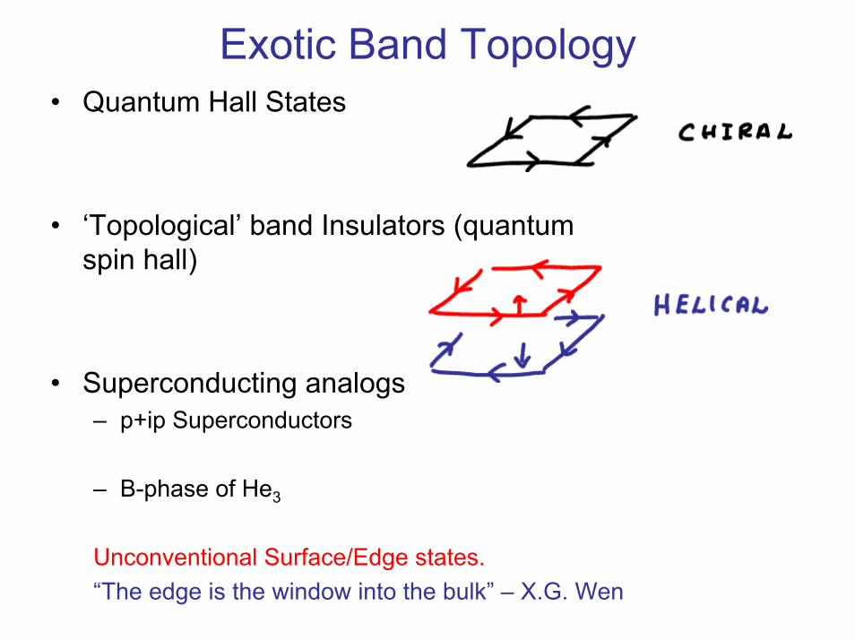
Exotic Band Topology• Quantum Hall States
• ‘Topological’ band Insulators (quantum spin hall)
• Superconducting analogs– p+ip Superconductors
– B-phase of He3
Unconventional Surface/Edge states. “The edge is the window into the bulk” – X.G. Wen

Broken Symmetry + Exotic Band Topology• Superconducting order parameter:• Vortex defects:
• Crystalline Solid – also broken symmetry phase.– Analog in topological insulators? YES
• Dislocations host counter-propagating 1D modes. Like the edge of 2D QSH Insulator - Helical Metal.
• Protected against disorder scattering – ideal quantum wire inside a bulk solid.
ϕie0Ψ
∫ =⋅∇ mdr πϕ 2
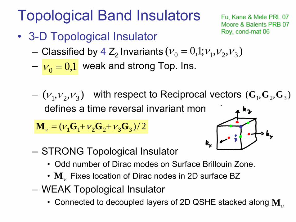
Topological Band Insulators• 3-D Topological Insulator
– Classified by 4 Z2 Invariants– weak and strong Top. Ins.
– with respect to Reciprocal vectors defines a time reversal invariant momentum
– STRONG Topological Insulator• Odd number of Dirac modes on Surface Brillouin Zone.• Fixes location of Dirac nodes in 2D surface BZ
– WEAK Topological Insulator• Connected to decoupled layers of 2D QSHE stacked along
),,;1,0( 3210 νννν =1,00 =ν
),,( 321 ννν ),,( 321 GGG
2/)( 321 GGGM 321 νννν ++=
νM
νM

Line Defects in a Crystal• Dislocations:Defined by location R(σ) and ‘strength’ B .
B – Burgers Vector, must stay constant along the length and is quantized to lattice vectors. (Like vorticity)

Visualizing Dislocations• Volterra Process:
– Cut with an imaginary plane, that ends on the dislocation line R(σ) – Move all atoms on one side of the plane by the Burgers vector B– Add/remove atoms if required.
SCREW DISLOCATION: t // B
B
EDGE DISLOCATION: t ┴ B
B

Dislocations in Solids• Always present • Control mechanical properties eg. Plastic Flow• Crystal Growth – aided by screw dislocations.
-2d m ton 1210 1010≈
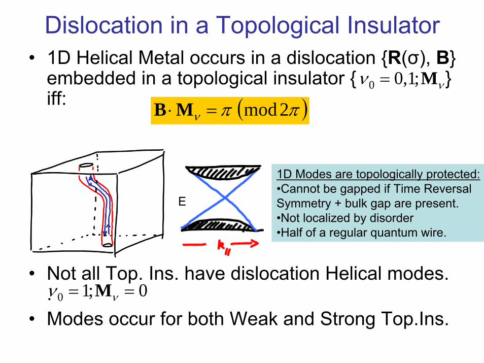
Dislocation in a Topological Insulator• 1D Helical Metal occurs in a dislocation {R(σ), B}
embedded in a topological insulator { } iff:
• Not all Top. Ins. have dislocation Helical modes. .
• Modes occur for both Weak and Strong Top.Ins.
νν M;1,00 =
( )ππν 2mod=⋅MB
E
1D Modes are topologically protected:•Cannot be gapped if Time Reversal Symmetry + bulk gap are present.•Not localized by disorder•Half of a regular quantum wire.
0;10 == νν M

Illustration – Diamond Lattice Top. Ins.
• Introduce a screw dislocation: B=(1,1,0).• Easily introduced in tight binding. Momentum dependent phase
factor for cut bonds.
)1,1,1(2
;10πν ν == M
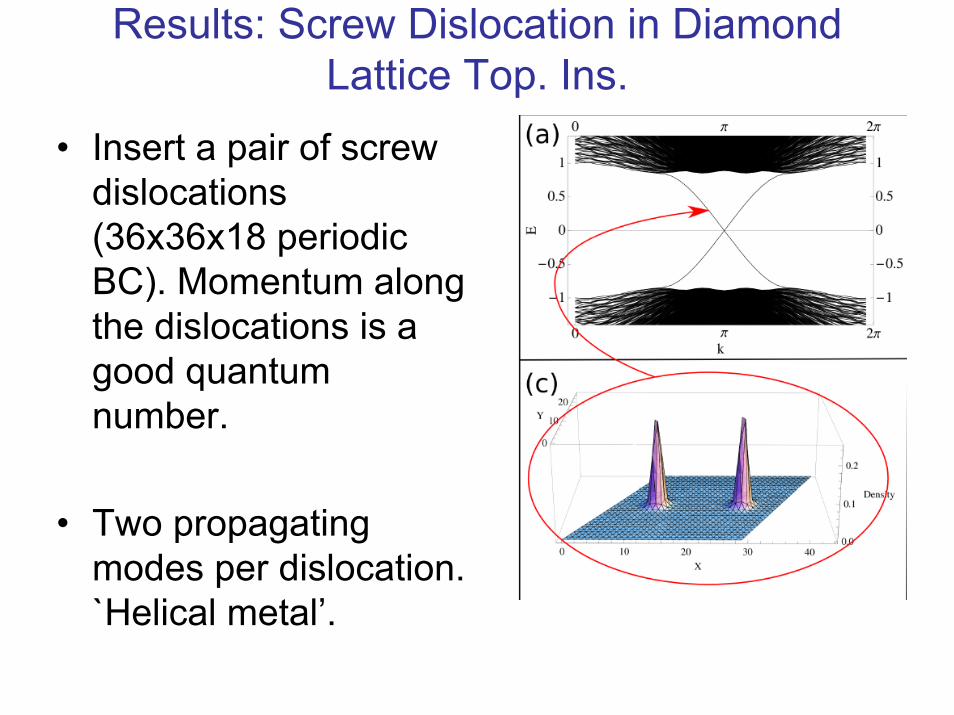
Results: Screw Dislocation in Diamond Lattice Top. Ins.
• Insert a pair of screw dislocations (36x36x18 periodic BC). Momentum along the dislocations is a good quantum number.
• Two propagating modes per dislocation. `Helical metal’.

Proof for Weak Top. Ins.• Weak Top.Ins. Adiabatically connected to a
stack of decoupled 2D Top.Ins., – stacking along – Different proof for Strong TI
νM
Cut Surface – only one of the helical mode pairs is shown.
Glued Surface – Dislocation must carry helical modes

Proof For General Top. Ins. 1
• Screw dislocation – if surface Dirac node is at momentum then (-1) phase acquired on crossing the dislocation.
• In the weak surface connection limit => Dirac equation that changes mass term sign.
π=⋅BmDirac
( ) xz xmppH μμσσ )( 22211 ++= mxmmxm
+=<−=>
)0()0(
2
2

Proof For General Top. Ins. 2
• Pair of zero modes at p1=0. • Propagating 1D helical modes for general p1.
• Location of Surface Dirac Node – controlled by
)2(mod ππ
π
ν =⋅⇓
=⋅
BM
BmDirac
( ) xz xmppH μμσσ )( 22211 ++=
mxmmxm
+=<−=>
)0()0(
2
2
')'(
02
2
0)(∫−
=
x
dxxm
ex ψψ
νM
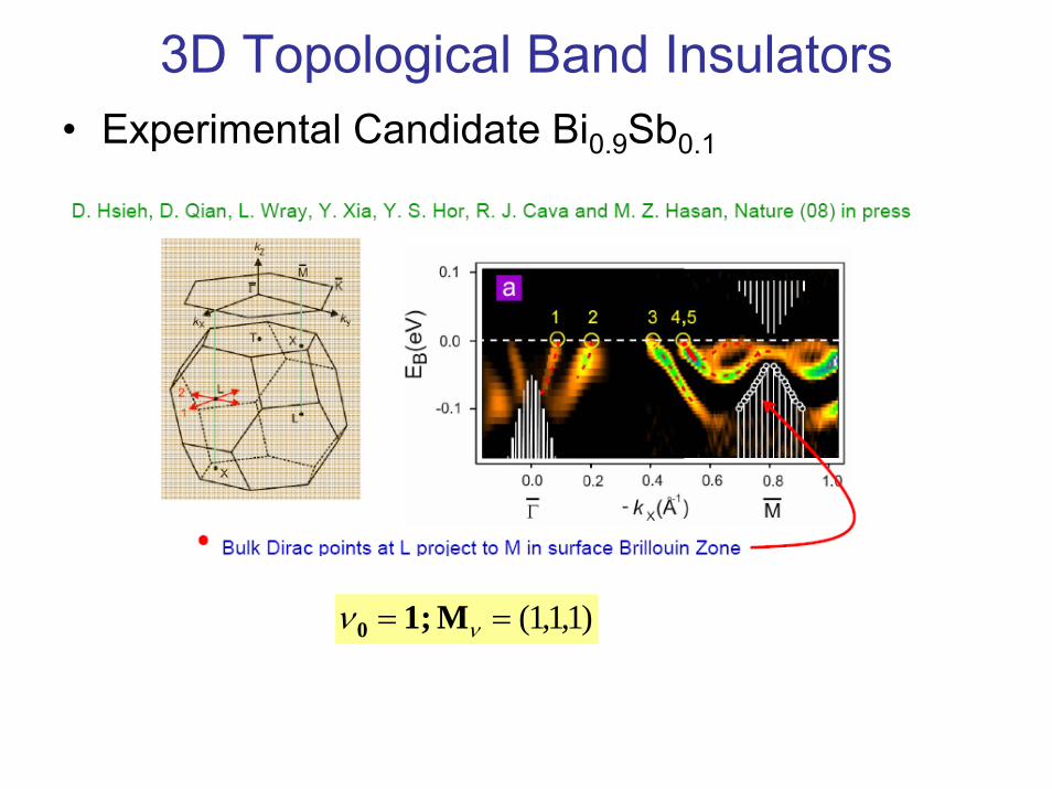
3D Topological Band Insulators • Experimental Candidate Bi0.9Sb0.1
)1,1,1(== νν M 1;0

Experimental Signatures• Resistivity: dislocation contribution could
dominate over surface conduction.
• Scanning Tunneling Microscopy: Can determine atomic defect structure and Local Density of States (LDOS). 1D modes – finite DOS. Dirac point – vanishing density of states.
ml μ1≈mΩ≈= −2
2 1012 dnlehρ
21210 −≈ mnd
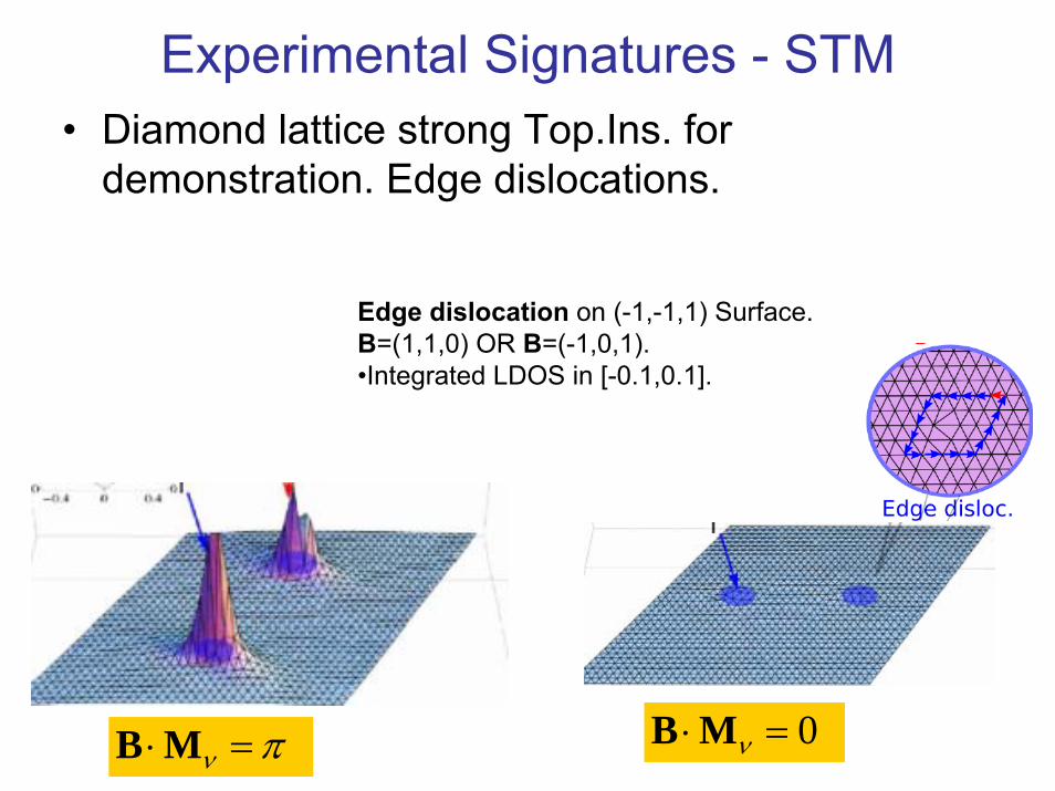
Experimental Signatures - STM• Diamond lattice strong Top.Ins. for
demonstration. Edge dislocations.
Edge dislocation on (-1,-1,1) Surface.B=(1,1,0) OR B=(-1,0,1). •Integrated LDOS in [-0.1,0.1].
πν =⋅MB 0=⋅ νMB

Effect of Disorder• Very Strong Disorder – dislocations proliferate;
no meaning to • Moderate disorder – dilute dislocation density.
Can still characterize using gapless modes in dislocations and define . Weak insulators can be defined even with disorder. but Surface states localized.
• However, if unit cell is doubled with wave-vector effective Now, elementary dislocations are
forbidden. (different from disorder)
νM
νM
νM0=νM

Conclusions• 3D topological Band Insulator has protected
helical mode in those dislocations that satisfy
• Indicates weak topological insulator stable to disorder if dislocations do not proliferate.
• Applications – quantum computing?• Interaction effects – Luttinger liquid physics?• Derivation from ‘field theory’?
( )ππν 2mod=⋅MB
Future Directions