TMS470R1x Inter-Integrated Circuit (I2C) Reference Guide (Rev. C)
70
TMS470R1x Inter-Integrated Circuit (I2C) Reference Guide Literature Number: SPNU223C February 2005
Transcript of TMS470R1x Inter-Integrated Circuit (I2C) Reference Guide (Rev. C)
TMS470R1x Inter-IntegratedCircuit (I2C)
Reference Guide
Literature Number: SPNU223CFebruary 2005
IMPORTANT NOTICE
Texas Instruments Incorporated and its subsidiaries (TI) reserve the right to make corrections, modifications, enhancements,improvements, and other changes to its products and services at any time and to discontinue any product or service withoutnotice. Customers should obtain the latest relevant information before placing orders and should verify that such information iscurrent and complete. All products are sold subject to TI’s terms and conditions of sale supplied at the time of orderacknowledgment.
TI warrants performance of its hardware products to the specifications applicable at the time of sale in accordance with TI’sstandard warranty. Testing and other quality control techniques are used to the extent TI deems necessary to support thiswarranty. Except where mandated by government requirements, testing of all parameters of each product is not necessarilyperformed.
TI assumes no liability for applications assistance or customer product design. Customers are responsible for their products andapplication s using TI components. To minimize the risks associated with customer products and applications, customers shouldprovide adequate design and operating safeguards.
TI does not warrant or represent that any license, either express or implied, is granted under any TI patent right, copyright, maskwork right, or other TI intellectual property right relating to any combination, machine, or process in which TI products or servicesare used. Information published by TI regarding third-party products or services does not constitute a license from TI to use suchproducts or services or a warranty or endorsement thereof. Use of such information may require a license from a third party underthe patents or other intellectual property of the third party, or a license from TI under the patents or other intellectual property of TI.
Reproduction of information in TI data books or data sheets is permissible only if reproduction is without alteration and isaccompanied by all associated warranties, conditions, limitations, and notices. Reproduction of this information with alteration isan unfair and deceptive business practice. TI is not responsible or liable for such altered documentation.
Resale of TI products or services with statements different form or beyond the parameters stated by TI for that product or servicevoids all express and any implied warranties for the associated TI product or service and is an unfair and deceptive businesspractice. TI is not responsible or liable for any such statements.
Following are URLs where you can obtain information on other Texas Instruments products and application solutions:
Mailing Address: Texas InstrumentsPost Office Box 655303 Dallas, Texas 75265
Copyright © 2005, Texas Instruments Incorporated
Products Applications
Amplifiers amplifier.ti.com Audio www.ti.com/audioData Converters dataconverter.ti.com Automotive www.ti.com/automotiveDSP dsp.ti.com Broadband www.ti.com/broadbandInterface interface.ti.com Digital Control www.ti.com/digitalcontrolLogic logic.ti.com Military www.ti.com/militaryPower Mgmt power.ti.com Optical Networking www.ti.com/opticalnetworkMicrocontrollers microcontroller.ti.com Security www.ti.com/security
Telephony www.ti.com/telephony
Video & Imaging www.ti.com/video
Wireless www.ti.com/wireless

REVISION HISTORY
REVISION DATE NOTES
C 12/04 Updates:
Throughout: updated operating frequency, clarified interrupt infor-mation, noted DIN/DOUT duplicate register function, and fixed bit descriptions for the second pair of DIN/DOUT registers.
page 6: changed reference to “specific data sheet” for module clock frequency to specific values.
page 20: Clarified when a new interrupt will be generated.
page 20: Updated TXRDY interrupt description.
page 21: Added description of how RXRDY and TXRDY bits are handled by a DMA access.
page 30: Corrected RXRDY and TXRDY bit descriptions.
page 35: Corrected CNT bit description. page 39: Corrected nIRS bit description. page 45: Corrected INTCODE bit description. page 57: Clarified register description.
B 11/03 Updates:Throughout, nine internal registers added to support new features of the I2C modulepage 6, section on clock generation added page 15, section on NACK bit generation addedpage 21, SCD and AAS interrupt requests addedpage 22, information on interrupt requests added
A 9/02 Converted to a stand-alone book
* 2/02 Initial version


Contents
1 Overview . . . . . . . . . . . . . . . . . . . . . . . . . . . . . . . . . . . . . . . . . . . . . . . . . . . . . . . . . . . . . . . . . . . 21.1 Introduction to the I2C Module . . . . . . . . . . . . . . . . . . . . . . . . . . . . . . . . . . . . . . . . . . . . . 31.2 Functional Overview . . . . . . . . . . . . . . . . . . . . . . . . . . . . . . . . . . . . . . . . . . . . . . . . . . . . . 31.3 Clock Generation . . . . . . . . . . . . . . . . . . . . . . . . . . . . . . . . . . . . . . . . . . . . . . . . . . . . . . . 5
2 I2C Register Overview . . . . . . . . . . . . . . . . . . . . . . . . . . . . . . . . . . . . . . . . . . . . . . . . . . . . . . . . 83 I2C Module Operation . . . . . . . . . . . . . . . . . . . . . . . . . . . . . . . . . . . . . . . . . . . . . . . . . . . . . . . 10
3.1 Input and Output Voltage Levels . . . . . . . . . . . . . . . . . . . . . . . . . . . . . . . . . . . . . . . . . . 103.2 I2C Module Reset Conditions. . . . . . . . . . . . . . . . . . . . . . . . . . . . . . . . . . . . . . . . . . . . . 103.3 I2C Module Data Validity . . . . . . . . . . . . . . . . . . . . . . . . . . . . . . . . . . . . . . . . . . . . . . . . 103.4 I2C Module Start and Stop Conditions . . . . . . . . . . . . . . . . . . . . . . . . . . . . . . . . . . . . . . 103.5 Serial Data Formats . . . . . . . . . . . . . . . . . . . . . . . . . . . . . . . . . . . . . . . . . . . . . . . . . . . . 11
3.5.1 7-Bit Addressing Format. . . . . . . . . . . . . . . . . . . . . . . . . . . . . . . . . . . . . . . . . . 123.5.2 10-Bit Addressing Format. . . . . . . . . . . . . . . . . . . . . . . . . . . . . . . . . . . . . . . . . 123.5.3 Using the Repeated START Condition. . . . . . . . . . . . . . . . . . . . . . . . . . . . . . . 133.5.4 Free Data Format . . . . . . . . . . . . . . . . . . . . . . . . . . . . . . . . . . . . . . . . . . . . . . . 13
3.6 NACK Bit Generation . . . . . . . . . . . . . . . . . . . . . . . . . . . . . . . . . . . . . . . . . . . . . . . . . . . 144 I2C Operation Modes . . . . . . . . . . . . . . . . . . . . . . . . . . . . . . . . . . . . . . . . . . . . . . . . . . . . . . . . 15
4.1 Master Transmitter Mode . . . . . . . . . . . . . . . . . . . . . . . . . . . . . . . . . . . . . . . . . . . . . . . . 154.2 Master Receiver Mode . . . . . . . . . . . . . . . . . . . . . . . . . . . . . . . . . . . . . . . . . . . . . . . . . . 154.3 Slave Transmitter Mode . . . . . . . . . . . . . . . . . . . . . . . . . . . . . . . . . . . . . . . . . . . . . . . . . 164.4 Slave Receiver Mode . . . . . . . . . . . . . . . . . . . . . . . . . . . . . . . . . . . . . . . . . . . . . . . . . . . 164.5 Low Power Mode . . . . . . . . . . . . . . . . . . . . . . . . . . . . . . . . . . . . . . . . . . . . . . . . . . . . . . 164.6 Free Run Mode. . . . . . . . . . . . . . . . . . . . . . . . . . . . . . . . . . . . . . . . . . . . . . . . . . . . . . . . 16
5 I2C Module Integrity . . . . . . . . . . . . . . . . . . . . . . . . . . . . . . . . . . . . . . . . . . . . . . . . . . . . . . . . . 175.1 Arbitration . . . . . . . . . . . . . . . . . . . . . . . . . . . . . . . . . . . . . . . . . . . . . . . . . . . . . . . . . . . . 175.2 I2C Clock Generation and Synchronization . . . . . . . . . . . . . . . . . . . . . . . . . . . . . . . . . . 185.3 Prescaler . . . . . . . . . . . . . . . . . . . . . . . . . . . . . . . . . . . . . . . . . . . . . . . . . . . . . . . . . . . . 195.4 Noise Filter . . . . . . . . . . . . . . . . . . . . . . . . . . . . . . . . . . . . . . . . . . . . . . . . . . . . . . . . . . . 19
6 Operational Information. . . . . . . . . . . . . . . . . . . . . . . . . . . . . . . . . . . . . . . . . . . . . . . . . . . . . . 206.1 I2C Module Interrupts . . . . . . . . . . . . . . . . . . . . . . . . . . . . . . . . . . . . . . . . . . . . . . . . . . . 20
6.1.1 I2C Interrupt Requests . . . . . . . . . . . . . . . . . . . . . . . . . . . . . . . . . . . . . . . . . . . 206.2 DMA Controller Events . . . . . . . . . . . . . . . . . . . . . . . . . . . . . . . . . . . . . . . . . . . . . . . . . . 216.3 I2C Enable/Disable. . . . . . . . . . . . . . . . . . . . . . . . . . . . . . . . . . . . . . . . . . . . . . . . . . . . . 226.4 General Purpose I/O. . . . . . . . . . . . . . . . . . . . . . . . . . . . . . . . . . . . . . . . . . . . . . . . . . . . 22
v
Contents
7 I2C Internal Registers . . . . . . . . . . . . . . . . . . . . . . . . . . . . . . . . . . . . . . . . . . . . . . . . . . . . . . . . 237.1 I2C Own Address Manager (I2COAR) . . . . . . . . . . . . . . . . . . . . . . . . . . . . . . . . . . . . . . 257.2 I2C Interrupt Mask Register (I2CIMR). . . . . . . . . . . . . . . . . . . . . . . . . . . . . . . . . . . . . . . 267.3 I2C Status Register (I2CSR) . . . . . . . . . . . . . . . . . . . . . . . . . . . . . . . . . . . . . . . . . . . . . . 287.4 I2C Clock Divider Low Register (I2CCKL) . . . . . . . . . . . . . . . . . . . . . . . . . . . . . . . . . . . 337.5 I2C Clock Control High Register (I2CCKH). . . . . . . . . . . . . . . . . . . . . . . . . . . . . . . . . . . 347.6 I2C Data Count Register (I2CCNT). . . . . . . . . . . . . . . . . . . . . . . . . . . . . . . . . . . . . . . . . 357.7 I2C Data Receive Register (I2CDRR). . . . . . . . . . . . . . . . . . . . . . . . . . . . . . . . . . . . . . . 367.8 I2C Slave Address Register (I2CSAR) . . . . . . . . . . . . . . . . . . . . . . . . . . . . . . . . . . . . . . 377.9 I2C Data Transmit Register (I2CDXR) . . . . . . . . . . . . . . . . . . . . . . . . . . . . . . . . . . . . . . 387.10 I2C Mode Register (I2CMDR) . . . . . . . . . . . . . . . . . . . . . . . . . . . . . . . . . . . . . . . . . . . . . 397.11 I2C Interrupt Vector Register (I2CIVR) . . . . . . . . . . . . . . . . . . . . . . . . . . . . . . . . . . . . . . 457.12 I2C Extended Mode Register (I2CEMDR) . . . . . . . . . . . . . . . . . . . . . . . . . . . . . . . . . . . 477.13 I2C Prescale Register (I2CPSC). . . . . . . . . . . . . . . . . . . . . . . . . . . . . . . . . . . . . . . . . . . 487.14 I2C Data Direction Register (I2CDIR) . . . . . . . . . . . . . . . . . . . . . . . . . . . . . . . . . . . . . . . 497.15 I2C Data Output Register (I2CDOUT). . . . . . . . . . . . . . . . . . . . . . . . . . . . . . . . . . . . . . . 517.16 I2C Data Input Register (I2CDIN) . . . . . . . . . . . . . . . . . . . . . . . . . . . . . . . . . . . . . . . . . . 527.17 I2C Pin Function Register (I2CPFNC) . . . . . . . . . . . . . . . . . . . . . . . . . . . . . . . . . . . . . . 537.18 I2C Pin Direction Register (I2CPDIR) . . . . . . . . . . . . . . . . . . . . . . . . . . . . . . . . . . . . . . . 547.19 I2C Data In Register (I2CDIN) . . . . . . . . . . . . . . . . . . . . . . . . . . . . . . . . . . . . . . . . . . . . 557.20 I2C Data Out Register (I2CDOUT) . . . . . . . . . . . . . . . . . . . . . . . . . . . . . . . . . . . . . . . . . 567.21 I2C Data Set Register (I2CDSET). . . . . . . . . . . . . . . . . . . . . . . . . . . . . . . . . . . . . . . . . . 577.22 I2C Data Clear Register (I2CDCLR) . . . . . . . . . . . . . . . . . . . . . . . . . . . . . . . . . . . . . . . . 587.23 I2C Peripheral ID Register 1 (I2CPID1) . . . . . . . . . . . . . . . . . . . . . . . . . . . . . . . . . . . . . 597.24 I2C Peripheral ID Register 2 (I2CPID2) . . . . . . . . . . . . . . . . . . . . . . . . . . . . . . . . . . . . . 60
vi
Figures
1 Multiple I2C Modules Connection Diagram . . . . . . . . . . . . . . . . . . . . . . . . . . . . . . . . . . . . . . . . 32 Simple I2C Block Diagram . . . . . . . . . . . . . . . . . . . . . . . . . . . . . . . . . . . . . . . . . . . . . . . . . . . . . 53 Clocking Diagram for the I2C Module. . . . . . . . . . . . . . . . . . . . . . . . . . . . . . . . . . . . . . . . . . . . . 64 Bit Transfer on the I2C Bus. . . . . . . . . . . . . . . . . . . . . . . . . . . . . . . . . . . . . . . . . . . . . . . . . . . . 105 I2C Module START and STOP Conditions . . . . . . . . . . . . . . . . . . . . . . . . . . . . . . . . . . . . . . . . 116 I2C Module Data Transfer. . . . . . . . . . . . . . . . . . . . . . . . . . . . . . . . . . . . . . . . . . . . . . . . . . . . . 117 I2C Module 7-Bit Addressing Format . . . . . . . . . . . . . . . . . . . . . . . . . . . . . . . . . . . . . . . . . . . . 138 I2C Module 10-bit Addressing Format . . . . . . . . . . . . . . . . . . . . . . . . . . . . . . . . . . . . . . . . . . . 139 I2C Module 7-Bit Addressing Format with Repeated START. . . . . . . . . . . . . . . . . . . . . . . . . . 1310 I2C Module in Free Data Format . . . . . . . . . . . . . . . . . . . . . . . . . . . . . . . . . . . . . . . . . . . . . . . 1411 Arbitration Procedure Between Two Master Transmitters. . . . . . . . . . . . . . . . . . . . . . . . . . . . . 1712 Synchronization of Two I2C Clock Generators During Arbitration . . . . . . . . . . . . . . . . . . . . . . 1813 I2C Own Address Manager Register (I2COAR). . . . . . . . . . . . . . . . . . . . . . . . . . . . . . . . . . . . 2514 I2C Interrupt Mask Register (I2CIMR) . . . . . . . . . . . . . . . . . . . . . . . . . . . . . . . . . . . . . . . . . . . 2615 I2C Status Register (I2CSR) . . . . . . . . . . . . . . . . . . . . . . . . . . . . . . . . . . . . . . . . . . . . . . . . . . 2816 I2C Clock Divider Low Register (I2CCKL). . . . . . . . . . . . . . . . . . . . . . . . . . . . . . . . . . . . . . . . 3317 I2C Clock Control High Register (I2CCKH) . . . . . . . . . . . . . . . . . . . . . . . . . . . . . . . . . . . . . . . 3418 I2C Data Count Register (I2CCNT). . . . . . . . . . . . . . . . . . . . . . . . . . . . . . . . . . . . . . . . . . . . . 3519 I2C Data Receive Register (I2CDRR) . . . . . . . . . . . . . . . . . . . . . . . . . . . . . . . . . . . . . . . . . . . 3620 I2C Slave Address Register (I2CSAR). . . . . . . . . . . . . . . . . . . . . . . . . . . . . . . . . . . . . . . . . . . 3721 I2C Data Transmit Register (I2CDXR) . . . . . . . . . . . . . . . . . . . . . . . . . . . . . . . . . . . . . . . . . . . 3822 I2C Mode Register (I2CMDR) . . . . . . . . . . . . . . . . . . . . . . . . . . . . . . . . . . . . . . . . . . . . . . . . . 3923 I2C Interrupt Vector Register (I2CIVR). . . . . . . . . . . . . . . . . . . . . . . . . . . . . . . . . . . . . . . . . . . 4524 I2C Extended Mode Register (I2CEMDR) . . . . . . . . . . . . . . . . . . . . . . . . . . . . . . . . . . . . . . . . 4725 I2C Prescale Register (I2CPSC) . . . . . . . . . . . . . . . . . . . . . . . . . . . . . . . . . . . . . . . . . . . . . . . 4826 I2C Data Direction Register (I2CDIR) . . . . . . . . . . . . . . . . . . . . . . . . . . . . . . . . . . . . . . . . . . . 4927 I2C Data Output Register (I2CDOUT) . . . . . . . . . . . . . . . . . . . . . . . . . . . . . . . . . . . . . . . . . . . 5128 I2C Data Input Register (I2CDIN). . . . . . . . . . . . . . . . . . . . . . . . . . . . . . . . . . . . . . . . . . . . . . . 5229 I2C Pin Function Register (I2CPFNC) . . . . . . . . . . . . . . . . . . . . . . . . . . . . . . . . . . . . . . . . . . . 5330 I2C Pin Direction Register (I2CPDIR) . . . . . . . . . . . . . . . . . . . . . . . . . . . . . . . . . . . . . . . . . . . 54
vii
31 I2C Data In Register (I2CDIN) . . . . . . . . . . . . . . . . . . . . . . . . . . . . . . . . . . . . . . . . . . . . . . . . 5532 I2C Data Out Register (I2CDOUT) . . . . . . . . . . . . . . . . . . . . . . . . . . . . . . . . . . . . . . . . . . . . 5633 I2C Data Set Register (I2CDSET) . . . . . . . . . . . . . . . . . . . . . . . . . . . . . . . . . . . . . . . . . . . . . 5734 I2C Data Clear Register (I2CDCLR) . . . . . . . . . . . . . . . . . . . . . . . . . . . . . . . . . . . . . . . . . . . . 5835 I2C Peripheral ID Register 1 (I2CPID1) . . . . . . . . . . . . . . . . . . . . . . . . . . . . . . . . . . . . . . . . . 5936 I2C Peripheral ID Register 2 (I2CPID2) . . . . . . . . . . . . . . . . . . . . . . . . . . . . . . . . . . . . . . . . . 60
viii
Tables
1 I2C Internal Registers . . . . . . . . . . . . . . . . . . . . . . . . . . . . . . . . . . . . . . . . . . . . . . . . . . . . . . . . 82 Ways to Generate a NACK Bit . . . . . . . . . . . . . . . . . . . . . . . . . . . . . . . . . . . . . . . . . . . . . . . . . 143 Interrupt Request Sources in the I2C Module . . . . . . . . . . . . . . . . . . . . . . . . . . . . . . . . . . . . . 204 I2C Control Register File Used With the TMS470 CPU . . . . . . . . . . . . . . . . . . . . . . . . . . . . . . 245 2C Own Address Manager Register (I2COAR) Field Descriptions . . . . . . . . . . . . . . . . . . . . 256 Correct Mode for Bits OA.9:0 . . . . . . . . . . . . . . . . . . . . . . . . . . . . . . . . . . . . . . . . . . . . . . . . . . 257 I2C Interrupt Mask Register (I2CIMR) Field Descriptions . . . . . . . . . . . . . . . . . . . . . . . . . . . . 268 I2C Status Register (I2CSR) Field Descriptions . . . . . . . . . . . . . . . . . . . . . . . . . . . . . . . . . . . 289 I2C Clock Divider Low Register (I2CCKL) Field Descriptions . . . . . . . . . . . . . . . . . . . . . . . . 3310 I2C Clock Control High Register (I2CCKH) Field Descriptions . . . . . . . . . . . . . . . . . . . . . . . 3411 I2C Data Count Register (I2CCNT) Field Descriptions . . . . . . . . . . . . . . . . . . . . . . . . . . . . . . 3512 I2C Data Receive Register (I2CDRR) Field Descriptions . . . . . . . . . . . . . . . . . . . . . . . . . . . 3613 I2C Slave Address Register (I2CSAR) Field Descriptions . . . . . . . . . . . . . . . . . . . . . . . . . . . 3714 Correct Modes for Bits SA[9:0]. . . . . . . . . . . . . . . . . . . . . . . . . . . . . . . . . . . . . . . . . . . . . . . . . 3715 I2C Data Transmit Register (I2CDXR) Field Descriptions . . . . . . . . . . . . . . . . . . . . . . . . . . . 3816 I2C Mode Register (I2CMDR) Field Descriptions . . . . . . . . . . . . . . . . . . . . . . . . . . . . . . . . . . 3917 I2C Module Condition, Bus Activity and Mode . . . . . . . . . . . . . . . . . . . . . . . . . . . . . . . . . . . . . 4318 I2C Module Operating Modes . . . . . . . . . . . . . . . . . . . . . . . . . . . . . . . . . . . . . . . . . . . . . . . . . 4319 Number of Bits Sent on Bus . . . . . . . . . . . . . . . . . . . . . . . . . . . . . . . . . . . . . . . . . . . . . . . . . . . 4420 I2C Interrupt Vector Register (I2CIVR) Field Descriptions . . . . . . . . . . . . . . . . . . . . . . . . . . . 4521 Interrupt Codes for INTCODE Bit . . . . . . . . . . . . . . . . . . . . . . . . . . . . . . . . . . . . . . . . . . . . . . . 4622 I2C Extended Mode Register (I2CEMDR) Field Descriptions. . . . . . . . . . . . . . . . . . . . . . . . . 4723 I2C Prescale Register (I2CPSC) Field Descriptions . . . . . . . . . . . . . . . . . . . . . . . . . . . . . . . . 4824 I2C Data Direction Register (I2CDIR) Field Descriptions . . . . . . . . . . . . . . . . . . . . . . . . . . . . 4925 I2C Data Output Register (I2CDOUT) Field Descriptions . . . . . . . . . . . . . . . . . . . . . . . . . . . . 5126 I2C Data Input Register (I2CDIN) Field Descriptions . . . . . . . . . . . . . . . . . . . . . . . . . . . . . . . 5227 I2C Pin Function Register (I2CPFNC) Field Descriptions. . . . . . . . . . . . . . . . . . . . . . . . . . . . 5328 I2C Pin Direction Register (I2CPDIR) Field Descriptions . . . . . . . . . . . . . . . . . . . . . . . . . . . . 5429 I2C Data In Register (I2CDIN) Field Descriptions. . . . . . . . . . . . . . . . . . . . . . . . . . . . . . . . . . 5530 I2C Data Out Register (I2CDOUT) Field Descriptions . . . . . . . . . . . . . . . . . . . . . . . . . . . . . . 56
ix
31 I2C Data Set Register (I2CDSET) Field Descriptions . . . . . . . . . . . . . . . . . . . . . . . . . . . . . . . 5732 I2C Data Clear Register (I2CDCLR) Field Descriptions . . . . . . . . . . . . . . . . . . . . . . . . . . . . . 5833 I2C Peripheral ID Register 1 (I2CPID1) Field Descriptions . . . . . . . . . . . . . . . . . . . . . . . . . . . 5934 I2C Peripheral ID Register 2 (I2CPID2) Field Descriptions . . . . . . . . . . . . . . . . . . . . . . . . . . . 60
x
Inter-Integrated Circuit (I2C)
The inter-integrated circuit (I2C or I2C) module is a multi-mastercommunication module providing an interface between the Texas Instruments(TI) TMS470 microcontroller and devices compliant with PhilipsSemiconductor I2C-bus specification version 2.1 and connected by an I2C-bus. Components connected externally are capable of transmitting/receiving1 to 8 bits to/from the TI TMS470 microcontroller. This module will supportany slave or master I2C compatible device.
Topic Page
1 Overview . . . . . . . . . . . . . . . . . . . . . . . . . . . . . . . . . . . . . . . . . . . . . . . . . . 2
2 I2C Register Overview . . . . . . . . . . . . . . . . . . . . . . . . . . . . . . . . . . . . . . . 8
3 I2C Module Operation . . . . . . . . . . . . . . . . . . . . . . . . . . . . . . . . . . . . . . 10
4 I2C Operation Modes . . . . . . . . . . . . . . . . . . . . . . . . . . . . . . . . . . . . . . . 15
5 I2C Module Integrity. . . . . . . . . . . . . . . . . . . . . . . . . . . . . . . . . . . . . . . . 17
6 Operational Information . . . . . . . . . . . . . . . . . . . . . . . . . . . . . . . . . . . . 20
7 I2C Internal Registers . . . . . . . . . . . . . . . . . . . . . . . . . . . . . . . . . . . . . . 23
Inter-Integrated Circuit (I2C) (SPNU223C) 1
Overview
1 Overview
The I2C module is designed to comply with the Philips I2C bus specification,v2.1 (The I2C Specification, Philips document number 9398 393 40011).
The I2C has the following features:
❏ Two external device pins
■ SDA (serial data pin)
■ SCL (serial clock pin)
❏ Bit/Byte format transfer
❏ 7-bit and 10-bit device addressing modes
❏ General call
❏ START byte
❏ Free data format
❏ Multi-master transmitter/ slave receiver modes
❏ Multi-master receiver/ slave transmitter mode
❏ Supports transfer rates of 100 kbps and 400 kbps (Phillips fast-mode rate)
❏ Two DMA events (read and write)
❏ One read/write and one illegal operation interrupt that can be used by theCPU.
❏ Operates with TMS470 core frequency from 6.7 MHz up
❏ Operates with module frequency between 6.7 MHz to 13.3 MHz
❏ Module enable/disable capability
Note:
This I2C module does not support:
❏ High-speed (HS) mode
❏ C-bus compatibility mode
2
Overview
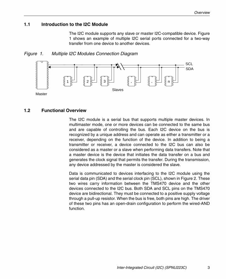
1.1 Introduction to the I2C Module
The I2C module supports any slave or master I2C-compatible device. Figure1 shows an example of multiple I2C serial ports connected for a two-waytransfer from one device to another devices.
Figure 1. Multiple I2C Modules Connection Diagram
1.2 Functional Overview
The I2C module is a serial bus that supports multiple master devices. Inmultimaster mode, one or more devices can be connected to the same busand are capable of controlling the bus. Each I2C device on the bus isrecognized by a unique address and can operate as either a transmitter or areceiver, depending on the function of the device. In addition to being atransmitter or receiver, a device connected to the I2C bus can also beconsidered as a master or a slave when performing data transfers. Note thata master device is the device that initiates the data transfer on a bus andgenerates the clock signal that permits the transfer. During the transmission,any device addressed by the master is considered the slave.
Data is communicated to devices interfacing to the I2C module using theserial data pin (SDA) and the serial clock pin (SCL), shown in Figure 2. Thesetwo wires carry information between the TMS470 device and the otherdevices connected to the I2C bus. Both SDA and SCL pins on the TMS470device are bidirectional. They must be connected to a positive supply voltagethrough a pull-up resistor. When the bus is free, both pins are high. The driverof these two pins has an open-drain configuration to perform the wired-ANDfunction.
1 2 3 . . n
SCLSDA
MasterSlaves
Inter-Integrated Circuit (I2C) (SPNU223C) 3
Overview
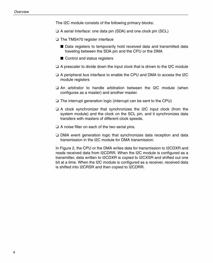
The I2C module consists of the following primary blocks:
❏ A serial Interface: one data pin (SDA) and one clock pin (SCL)
❏ The TMS470 register interface
■ Data registers to temporarily hold received data and transmitted datatraveling between the SDA pin and the CPU or the DMA
■ Control and status registers
❏ A prescaler to divide down the input clock that is driven to the I2C module
❏ A peripheral bus interface to enable the CPU and DMA to access the I2Cmodule registers
❏ An arbitrator to handle arbitration between the I2C module (whenconfigures as a master) and another master.
❏ The interrupt generation logic (interrupt can be sent to the CPU)
❏ A clock synchronizer that synchronizes the I2C input clock (from thesystem module) and the clock on the SCL pin, and it synchronizes datatransfers with masters of different clock speeds.
❏ A noise filter on each of the two serial pins.
❏ DMA event generation logic that synchronizes data reception and datatransmission in the I2C module for DMA transmission.
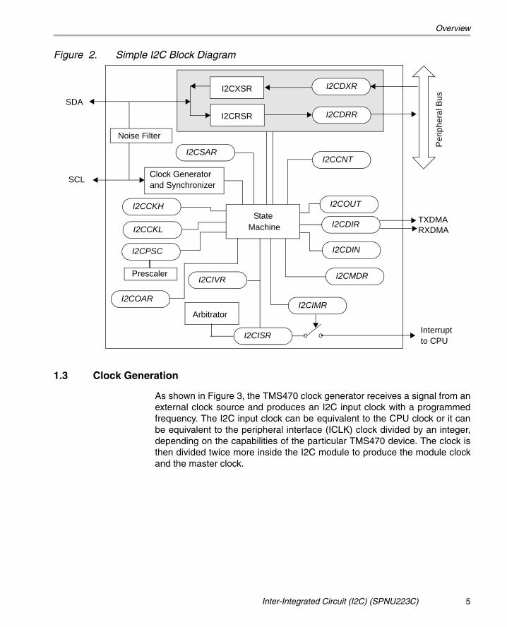
In Figure 2, the CPU or the DMA writes data for transmission to I2CDXR andreads received data from I2CDRR. When the I2C module is configured as atransmitter, data written to I2CDXR is copied to I2CXSR and shifted out onebit at a time. When the I2C module is configured as a receiver, received datais shifted into I2CRSR and then copied to I2CDRR.
4
Overview
Figure 2. Simple I2C Block Diagram
1.3 Clock Generation
As shown in Figure 3, the TMS470 clock generator receives a signal from anexternal clock source and produces an I2C input clock with a programmedfrequency. The I2C input clock can be equivalent to the CPU clock or it canbe equivalent to the peripheral interface (ICLK) clock divided by an integer,depending on the capabilities of the particular TMS470 device. The clock isthen divided twice more inside the I2C module to produce the module clockand the master clock.
I2CXSR
I2CRSR
I2CIVR
I2CIMR
I2CISR
Arbitrator
SDA
Perip
hera
l Bus
StateMachine
I2CDXR
I2CDRR
I2CMDR
Clock Generatorand SynchronizerSCL
I2CPSC
I2CCNT
I2COUT
I2CDIR
I2CDIN
I2CCKL
I2CCKH
Noise Filter
Prescaler
Interruptto CPU
TXDMARXDMA
I2COAR
I2CSAR
Inter-Integrated Circuit (I2C) (SPNU223C) 5

Overview
Figure 3. Clocking Diagram for the I2C Module
The module clock determines the frequency at which the I2C moduleoperates. A programmable prescaler in the I2C module divides down theinput clock to produce the module clock. To specify the divide-down value,initialize the I2CPSC field of the prescaler register, I2CPSC. The resultingfrequency is
(EQ 1)
The module clock frequency must be between 6.7MHz and 13.3MHz. Theprescaler can only be initialized while the I2C module is in the reset state (IRS= 0 in I2CMDR). The prescaled frequency takes effect only when IRS ischanged to 1. Changing the I2CPSC value while IRS = 1 has no effect.
The master clock appears on the SCL pin when the I2C module is configuredto be a master on the I2C bus. This clock controls the timing of thecommunication between the I2C module and a slave. As shown in Figure 3,a second clock divider in the I2C module divides down the module clock toproduce the master clock. The clock divider uses the I2CCKL to divide downthe low portion of the module clock signal and uses the I2CKH to divide downthe high portion of the module clock signal.
TMS470
GeneratorClock
OSCIN
TMS470
I2C Module
(ICLK)
I2C Input Clock
I2CPSCI2CCKLI2CCKH
Module Clock forI2C Module Operation
on SCL pin
Master ClockTo I2C Bus
ModuleClockFrequency I2CInputClockFrequencyI2CPSC 1+( )
--------------------------------------------------------------------=
6
Overview
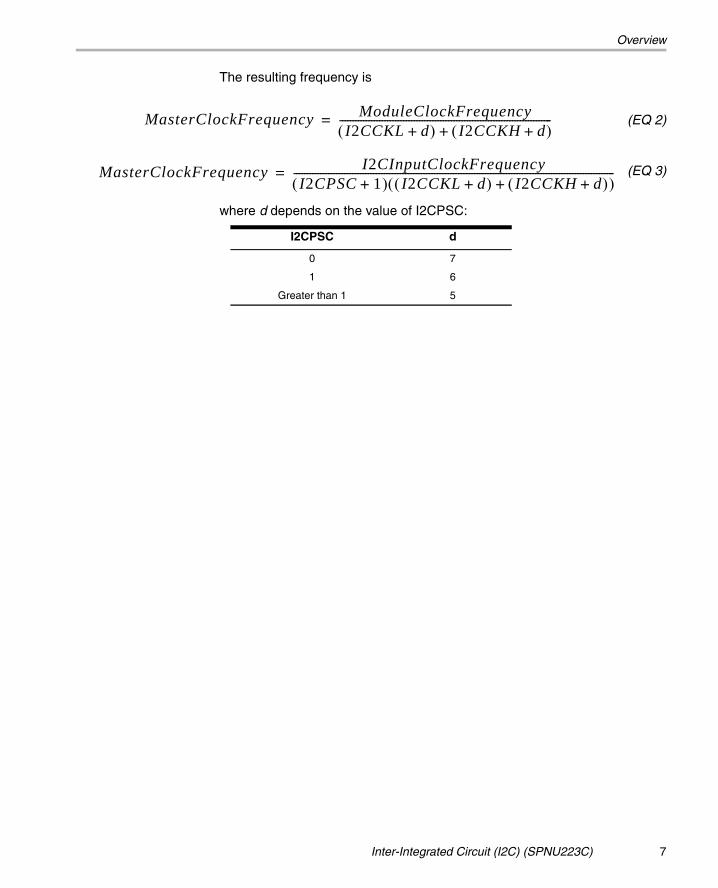
The resulting frequency is
(EQ 2)
(EQ 3)
where d depends on the value of I2CPSC:
I2CPSC d
0 7
1 6
Greater than 1 5
MasterClockFrequency ModuleClockFrequencyI2CCKL d+( ) I2CCKH d+( )+
--------------------------------------------------------------------------------=
MasterClockFrequency I2CInputClockFrequencyI2CPSC 1+( ) I2CCKL d+( ) I2CCKH d+( )+( )
-------------------------------------------------------------------------------------------------------------------------=
Inter-Integrated Circuit (I2C) (SPNU223C) 7
I2C Register Overview
2 I2C Register Overview
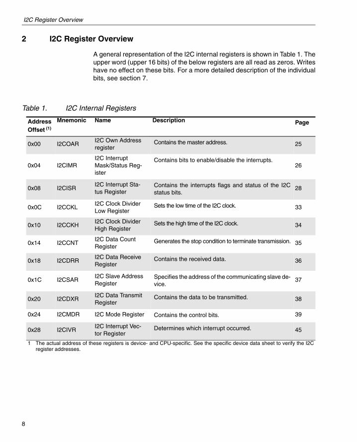
A general representation of the I2C internal registers is shown in Table 1. Theupper word (upper 16 bits) of the below registers are all read as zeros. Writeshave no effect on these bits. For a more detailed description of the individualbits, see section 7.
Table 1. I2C Internal Registers
Address Offset (1)
Mnemonic Name Description Page
0x00 I2COARI2C Own Address register
Contains the master address. 25
0x04 I2CIMRI2C Interrupt Mask/Status Reg-ister
Contains bits to enable/disable the interrupts.26
0x08 I2CISRI2C Interrupt Sta-tus Register
Contains the interrupts flags and status of the I2Cstatus bits.
28
0x0C I2CCKLI2C Clock Divider Low Register
Sets the low time of the I2C clock. 33
0x10 I2CCKHI2C Clock Divider High Register
Sets the high time of the I2C clock. 34
0x14 I2CCNTI2C Data Count Register
Generates the stop condition to terminate transmission. 35
0x18 I2CDRRI2C Data Receive Register
Contains the received data. 36
0x1C I2CSARI2C Slave Address Register
Specifies the address of the communicating slave de-vice.
37
0x20 I2CDXRI2C Data Transmit Register
Contains the data to be transmitted. 38
0x24 I2CMDR I2C Mode Register Contains the control bits. 39
0x28 I2CIVRI2C Interrupt Vec-tor Register
Determines which interrupt occurred. 45
1 The actual address of these registers is device- and CPU-specific. See the specific device data sheet to verify the I2Cregister addresses.
8
I2C Register Overview
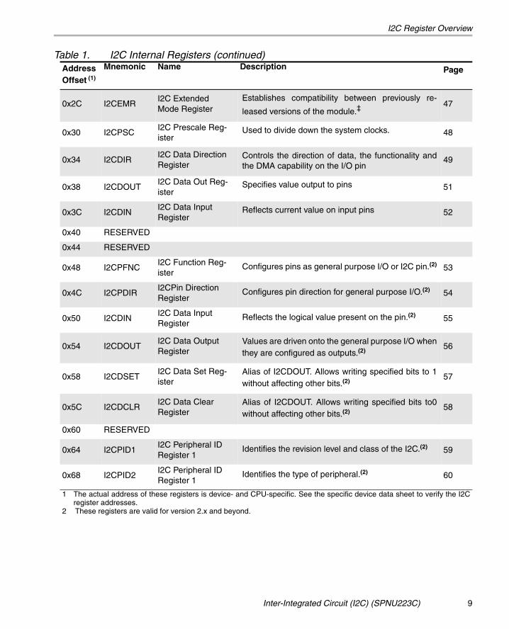
Table 1. I2C Internal Registers (continued)Address Offset (1)
Mnemonic Name Description Page
0x2C I2CEMRI2C Extended Mode Register
Establishes compatibility between previously re-
leased versions of the module.‡47
0x30 I2CPSCI2C Prescale Reg-ister
Used to divide down the system clocks. 48
0x34 I2CDIRI2C Data Direction Register
Controls the direction of data, the functionality andthe DMA capability on the I/O pin
49
0x38 I2CDOUTI2C Data Out Reg-ister
Specifies value output to pins 51
0x3C I2CDINI2C Data Input Register
Reflects current value on input pins 52
0x40 RESERVED
0x44 RESERVED
0x48 I2CPFNCI2C Function Reg-ister
Configures pins as general purpose I/O or I2C pin.(2) 53
0x4C I2CPDIRI2CPin Direction Register
Configures pin direction for general purpose I/O.(2) 54
0x50 I2CDINI2C Data Input Register
Reflects the logical value present on the pin.(2) 55
0x54 I2CDOUTI2C Data Output Register
Values are driven onto the general purpose I/O whenthey are configured as outputs.(2)
56
0x58 I2CDSETI2C Data Set Reg-ister
Alias of I2CDOUT. Allows writing specified bits to 1without affecting other bits.(2)
57
0x5C I2CDCLRI2C Data Clear Register
Alias of I2CDOUT. Allows writing specified bits to0without affecting other bits.(2)
58
0x60 RESERVED
0x64 I2CPID1I2C Peripheral ID Register 1
Identifies the revision level and class of the I2C.(2) 59
0x68 I2CPID2I2C Peripheral ID Register 1
Identifies the type of peripheral.(2) 60
1 The actual address of these registers is device- and CPU-specific. See the specific device data sheet to verify the I2Cregister addresses.
2 These registers are valid for version 2.x and beyond.
Inter-Integrated Circuit (I2C) (SPNU223C) 9

I2C Module Operation
3 I2C Module Operation
3.1 Input and Output Voltage Levels
One clock pulse is generated by the master device for each data bittransferred. Because of a variety of different technology devices that can beconnected to the I2C-bus, the levels of logic 0 (low) and logic 1 (high) are notfixed and depend on the associated level of VDDIO. For detail, see the devicespecific data sheet.
3.2 I2C Module Reset Conditions
The I2C module can be reset in the following two ways:
❏ Through the internal global peripheral reset.
❏ By clearing the IRS bit in the I2C mode register (I2CMDR). When thesystem peripheral reset is removed, the IRS bit is cleared to 0, keeping theI2C module in reset.
3.3 I2C Module Data Validity
The data on SDA must be stable during the high period of the clock. SeeFigure 4. The high and low state of the data line, SDA, can only change whenthe clock signal is low.
Figure 4. Bit Transfer on the I2C Bus
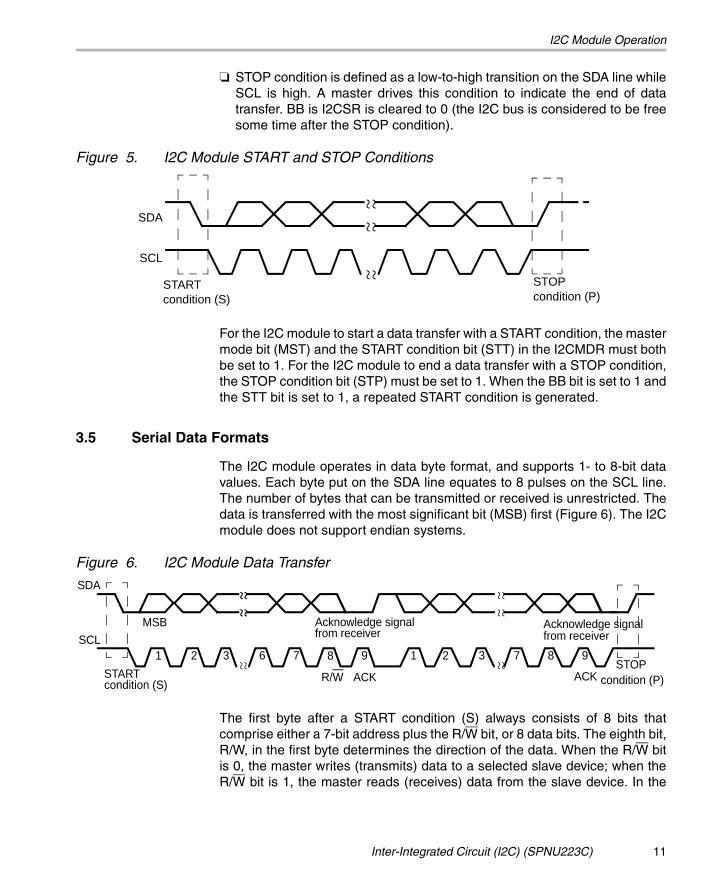
3.4 I2C Module Start and Stop Conditions
START and STOP conditions are generated by a master I2C module.
❏ START condition is defined as a high-to-low transition on the SDA linewhile SCL is high. A master drives this condition to indicate the start of datatransfer. The bus busy bit (BB) in I2CSR is set to 1 (the I2C bus isconsidered to be busy).
Data line
SDA
SCL
stable data
Change ofdata allowed
10
I2C Module Operation
❏ STOP condition is defined as a low-to-high transition on the SDA line whileSCL is high. A master drives this condition to indicate the end of datatransfer. BB is I2CSR is cleared to 0 (the I2C bus is considered to be freesome time after the STOP condition).
Figure 5. I2C Module START and STOP Conditions
For the I2C module to start a data transfer with a START condition, the mastermode bit (MST) and the START condition bit (STT) in the I2CMDR must bothbe set to 1. For the I2C module to end a data transfer with a STOP condition,the STOP condition bit (STP) must be set to 1. When the BB bit is set to 1 andthe STT bit is set to 1, a repeated START condition is generated.
3.5 Serial Data Formats
The I2C module operates in data byte format, and supports 1- to 8-bit datavalues. Each byte put on the SDA line equates to 8 pulses on the SCL line.The number of bytes that can be transmitted or received is unrestricted. Thedata is transferred with the most significant bit (MSB) first (Figure 6). The I2Cmodule does not support endian systems.
Figure 6. I2C Module Data Transfer
The first byte after a START condition (S) always consists of 8 bits thatcomprise either a 7-bit address plus the R/W bit, or 8 data bits. The eighth bit,R/W, in the first byte determines the direction of the data. When the R/W bitis 0, the master writes (transmits) data to a selected slave device; when theR/W bit is 1, the master reads (receives) data from the slave device. In the
~ ~~ ~
~ ~SDA
SCL
STARTcondition (S)
STOPcondition (P)
~ ~~ ~
~ ~~ ~
~ ~ ~ ~
SDA
SCL
STARTcondition (S)
STOPcondition (P)
MSB
1 2 6 7 8 9 1 2 3 7 8 9
R/W ACK ACK
Acknowledge signalfrom receiver
Acknowledge signalfrom receiver
~ ~~ ~
3
Inter-Integrated Circuit (I2C) (SPNU223C) 11
I2C Module Operation
acknowledge mode, an extra bit dedicated for the acknowledgement (ACK)bit, is inserted after each byte.
The I2C module supports the following formats:
❏ 7-bit addressing format (Figure 7)
❏ 10-bit addressing format (Figure 8)
❏ 7-bit/10-bit addressing format with repeated START condition (Figure 9)
❏ Free-data format (Figure 10)
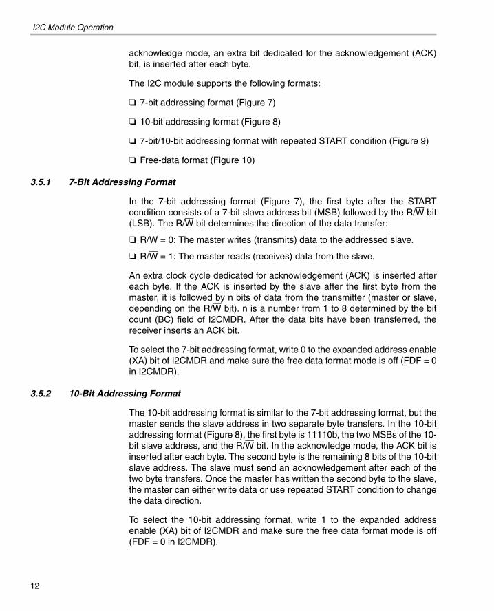
3.5.1 7-Bit Addressing Format
In the 7-bit addressing format (Figure 7), the first byte after the STARTcondition consists of a 7-bit slave address bit (MSB) followed by the R/W bit(LSB). The R/W bit determines the direction of the data transfer:
❏ R/W = 0: The master writes (transmits) data to the addressed slave.
❏ R/W = 1: The master reads (receives) data from the slave.
An extra clock cycle dedicated for acknowledgement (ACK) is inserted aftereach byte. If the ACK is inserted by the slave after the first byte from themaster, it is followed by n bits of data from the transmitter (master or slave,depending on the R/W bit). n is a number from 1 to 8 determined by the bitcount (BC) field of I2CMDR. After the data bits have been transferred, thereceiver inserts an ACK bit.
To select the 7-bit addressing format, write 0 to the expanded address enable(XA) bit of I2CMDR and make sure the free data format mode is off (FDF = 0in I2CMDR).
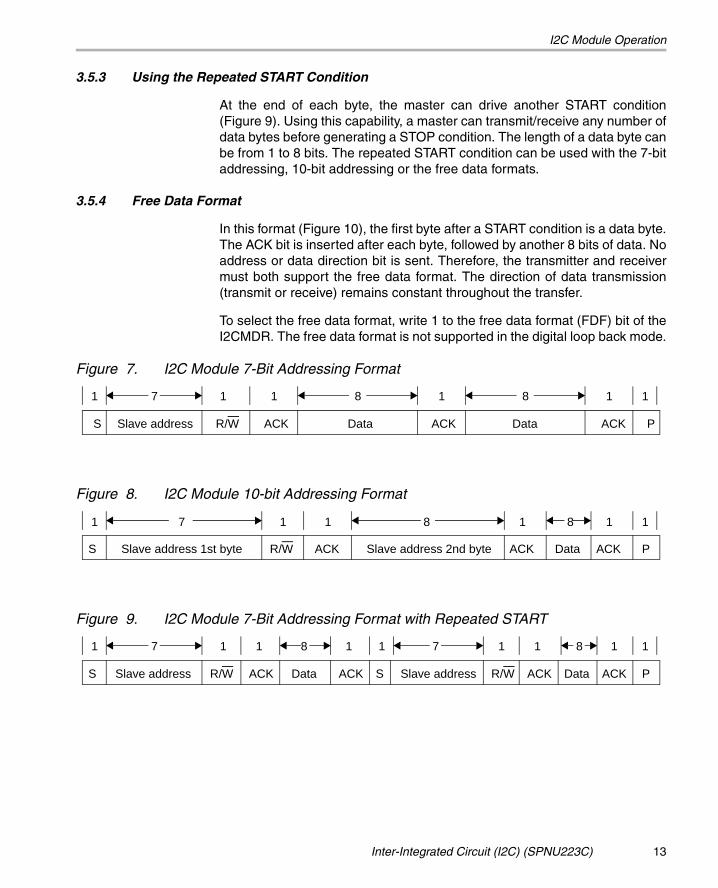
3.5.2 10-Bit Addressing Format
The 10-bit addressing format is similar to the 7-bit addressing format, but themaster sends the slave address in two separate byte transfers. In the 10-bitaddressing format (Figure 8), the first byte is 11110b, the two MSBs of the 10-bit slave address, and the R/W bit. In the acknowledge mode, the ACK bit isinserted after each byte. The second byte is the remaining 8 bits of the 10-bitslave address. The slave must send an acknowledgement after each of thetwo byte transfers. Once the master has written the second byte to the slave,the master can either write data or use repeated START condition to changethe data direction.
To select the 10-bit addressing format, write 1 to the expanded addressenable (XA) bit of I2CMDR and make sure the free data format mode is off(FDF = 0 in I2CMDR).
12
I2C Module Operation
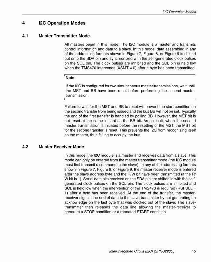
3.5.3 Using the Repeated START Condition
At the end of each byte, the master can drive another START condition(Figure 9). Using this capability, a master can transmit/receive any number ofdata bytes before generating a STOP condition. The length of a data byte canbe from 1 to 8 bits. The repeated START condition can be used with the 7-bitaddressing, 10-bit addressing or the free data formats.
3.5.4 Free Data Format
In this format (Figure 10), the first byte after a START condition is a data byte.The ACK bit is inserted after each byte, followed by another 8 bits of data. Noaddress or data direction bit is sent. Therefore, the transmitter and receivermust both support the free data format. The direction of data transmission(transmit or receive) remains constant throughout the transfer.
To select the free data format, write 1 to the free data format (FDF) bit of theI2CMDR. The free data format is not supported in the digital loop back mode.
Figure 7. I2C Module 7-Bit Addressing Format
Figure 8. I2C Module 10-bit Addressing Format
Figure 9. I2C Module 7-Bit Addressing Format with Repeated START
S Slave address R/W ACK Data ACK Data ACK P
1 1 17 8 1 8 1 1
1
S Slave address 1st byte R/W ACK Slave address 2nd byte ACK Data ACK P
1 17 8 1 8 1 1
S Slave address R/W ACK Data ACK Data ACK P
1 1 17 8 1 8 1 1
Slave address
7
S R/W ACK
1 1 1
Inter-Integrated Circuit (I2C) (SPNU223C) 13

I2C Module Operation
Figure 10. I2C Module in Free Data Format
3.6 NACK Bit Generation
When the I2C module is a receiver (master or slave), it can acknowledge orignore bits sent by the transmitter. To ignore any new bits, the I2C modulemust send a no-acknowledge (NACK) bit during the acknowledge cycle onthe bus. Table 2 summarizes the various ways a NACK can be generated.
Table 2. Ways to Generate a NACK Bit
1 Unsupported on versions released before 2.x.
I2C Module Condition Basic NACK Bit Generation Options Additional Option(1)
Slave Receiver Mode
❏ Disable data transfers (STT = 0)❏ Allow an overrun condition (RSFULL = 1)❏ Reset the module (IRS = 0)
Set the NACKMOD bit before the rising edge of the last data bit you intend to receive.
Master Receiver Mode and Repeat Mode (RM = 1)
❏ Generate a STOP condition (STP = 1)❏ Reset the module (IRS = 0)
Set the NACKMOD bit before the rising edge of the last data bit you intend to receive.
Master Receiver Mode with Non-Repeat Mode (RM = 0)
❏ If STP = 1, allow the internal data counterto count down to 0 and thus force aSTOP condition.
❏ If STP = 0, make STP = 1 to generate aSTOP condition.
❏ Reset the module (IRS = 0)
Set the NACKMOD bit before the rising edge of the last data bit you intend to receive.
S Data ACK Data ACK Data ACK P
1 18 8 1 8 1 1
14
I2C Operation Modes
4 I2C Operation Modes
4.1 Master Transmitter Mode
All masters begin in this mode. The I2C module is a master and transmitscontrol information and data to a slave. In this mode, data assembled in anyof the addressing formats shown in Figure 7, Figure 8, or Figure 9 is shiftedout onto the SDA pin and synchronized with the self-generated clock pulseson the SCL pin. The clock pulses are inhibited and the SCL pin is held lowwhen the TMS470 intervenes (XSMT = 0) after a byte has been transmitted.
Note:
If the I2C is configured for two simultaneous master transmissions, wait untilthe MST and BB have been reset before performing the second mastertransmission.
Failure to wait for the MST and BB to reset will prevent the start condition onthe second transfer from being issued and the bus BB will not be set. Typicallythe end of the first transfer is handled by polling BB. However, the MST bit isnot reset at the same instant as the BB bit. As a result, when the secondmaster transmission is initiated before the resetting of the MST, the MST bitfor the second transfer is reset. This prevents the I2C from recognizing itselfas the master, thus failing to occupy the bus.
4.2 Master Receiver Mode
In this mode, the I2C module is a master and receives data from a slave. Thismode can only be entered from the master transmitter mode (the I2C modulemust first transmit a command to the slave). In any of the addressing formatsshown in Figure 7, Figure 8, or Figure 9, the master receiver mode is enteredafter the slave address byte and the R/W bit have been transmitted (if the R/W bit is 1). Serial data bits received on the SDA pin are shifted in with the self-generated clock pulses on the SCL pin. The clock pulses are inhibited andSCL is held low when the intervention of the TMS470 is required (RSFULL =1) after a byte has been received. At the end of the transfer, the master-receiver signals the end of data to the slave-transmitter by not generating anacknowledge on the last byte that was clocked out of the slave. The slave-transmitter then releases the data line allowing the master-receiver togenerate a STOP condition or a repeated START condition.
Inter-Integrated Circuit (I2C) (SPNU223C) 15
I2C Operation Modes
4.3 Slave Transmitter Mode
In this mode, the I2C module is a slave and transmits data to a master. Thismode can only be entered from the slave receiver mode (The I2C modulemust first receive a command from the master). In any of the addressingformats shown in Figure 7, Figure 8, or Figure 9, the slave transmitter modeis entered if the slave address byte is the same as its own address and the R/W bit has been transmitted (if the R/W bit is set to 1). The slave transmittershifts the serial data out on the SDA pin with the clock pulses that aregenerated by the master device. The slave device does not generate theclock, but the SCL pin is held low when the TMS470 intervenes (XSMT = 0)after a byte has been transmitted.
4.4 Slave Receiver Mode
In this mode, the I2C module is a slave and receives data from a master. Allslaves begin in this mode. Serial data bits received on the SDA pin are shiftedin with the clock pulses that are generated by the master device. The slavedevice does not generate the clock, but it can hold the SCL pin low whileintervention of the TMS470 is required (RSFULL = 1) after a byte has beenreceived.
4.5 Low Power Mode
The I2C module can be placed in low-power mode by a global low-powermode initiated by the system, or by a local low-power mode initiated by theLPM bit (I2CMDR.12). The net effect on the I2C is the same, independent ofthe source of the command.
In effect, low-power mode shuts down all the clocks to the module. In globallow-power mode, no registers are visible to the software; nothing can bewritten to or read from any register. Local low-power mode has the sameeffect, with the exception that only the LPM bit can be written to, whichenables placing the I2C module into a functional mode.
4.6 Free Run Mode
The I2C module can be placed in free run mode when the FREE bit(I2CMDR.14) is set to 1. This bit is primarily used on an emulator whenencountering a breakpoint while debugging software. When the FREE bit isset to 0, the I2C responds differently depending on whether SCL is high orlow. If SCL is low, the I2C stops immediately and keeps driving SCL lowwhether the I2C is the master transmitter or receiver. If SCL is high, the I2Cwaits until SCL becomes a low and then stops. If the I2C is a slave, it stopswhen the transmission/reception completes.
16
I2C Module Integrity
5 I2C Module Integrity
The following sections discuss how the I2C module maintains priorities andorder among signals and commands.
5.1 Arbitration
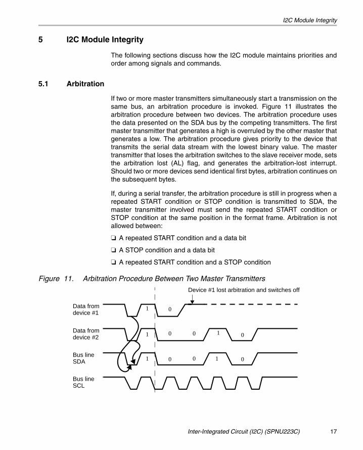
If two or more master transmitters simultaneously start a transmission on thesame bus, an arbitration procedure is invoked. Figure 11 illustrates thearbitration procedure between two devices. The arbitration procedure usesthe data presented on the SDA bus by the competing transmitters. The firstmaster transmitter that generates a high is overruled by the other master thatgenerates a low. The arbitration procedure gives priority to the device thattransmits the serial data stream with the lowest binary value. The mastertransmitter that loses the arbitration switches to the slave receiver mode, setsthe arbitration lost (AL) flag, and generates the arbitration-lost interrupt.Should two or more devices send identical first bytes, arbitration continues onthe subsequent bytes.
If, during a serial transfer, the arbitration procedure is still in progress when arepeated START condition or STOP condition is transmitted to SDA, themaster transmitter involved must send the repeated START condition orSTOP condition at the same position in the format frame. Arbitration is notallowed between:
❏ A repeated START condition and a data bit
❏ A STOP condition and a data bit
❏ A repeated START condition and a STOP condition
Figure 11. Arbitration Procedure Between Two Master Transmitters
Bus lineSCL
Data fromdevice #1
Data fromdevice #2
Bus lineSDA
1
1
1
1
1
0 0
00
0
Device #1 lost arbitration and switches off
0
0
Inter-Integrated Circuit (I2C) (SPNU223C) 17
I2C Module Integrity
5.2 I2C Clock Generation and Synchronization
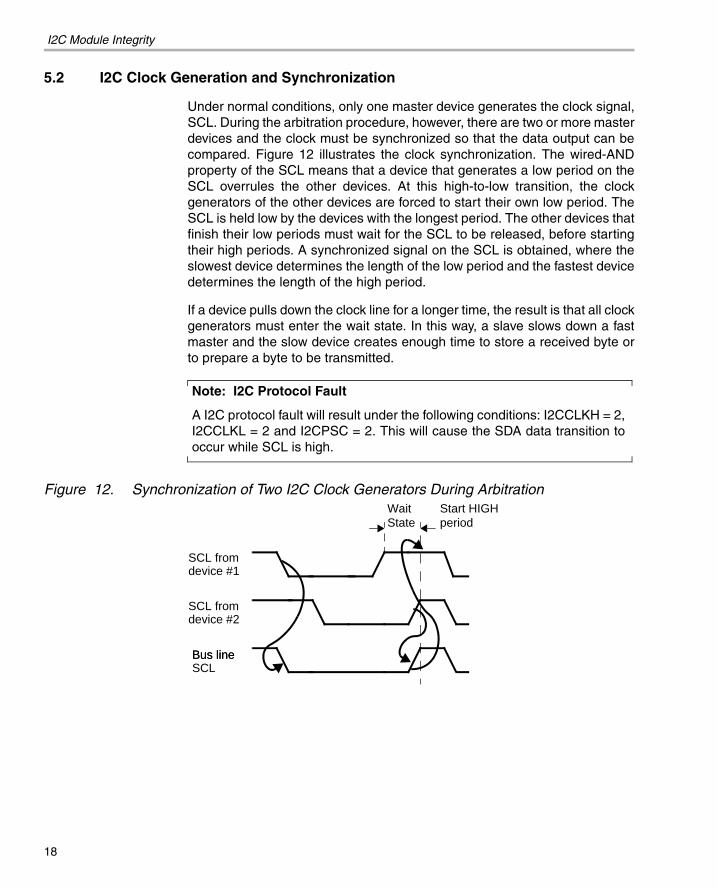
Under normal conditions, only one master device generates the clock signal,SCL. During the arbitration procedure, however, there are two or more masterdevices and the clock must be synchronized so that the data output can becompared. Figure 12 illustrates the clock synchronization. The wired-ANDproperty of the SCL means that a device that generates a low period on theSCL overrules the other devices. At this high-to-low transition, the clockgenerators of the other devices are forced to start their own low period. TheSCL is held low by the devices with the longest period. The other devices thatfinish their low periods must wait for the SCL to be released, before startingtheir high periods. A synchronized signal on the SCL is obtained, where theslowest device determines the length of the low period and the fastest devicedetermines the length of the high period.
If a device pulls down the clock line for a longer time, the result is that all clockgenerators must enter the wait state. In this way, a slave slows down a fastmaster and the slow device creates enough time to store a received byte orto prepare a byte to be transmitted.
Note: I2C Protocol Fault
A I2C protocol fault will result under the following conditions: I2CCLKH = 2,I2CCLKL = 2 and I2CPSC = 2. This will cause the SDA data transition tooccur while SCL is high.
Figure 12. Synchronization of Two I2C Clock Generators During Arbitration
Bus line
SCL from
SCL from
SCL
device #2
device #1
WaitState
Start HIGHperiod
Bus line
18
I2C Module Integrity
5.3 Prescaler
The I2C module is operated by the module clock. This clock is generated byway of the I2C prescaler block. The prescaler block consists of a 16-bitregister, I2CPSC, used for dividing down the interface clock (ICLK) to obtaina module clock between 6.7 MHz and 13.3 MHz.
5.4 Noise Filter
The noise filter is used to suppress any noises that are 50 ns or less. It isdesigned to suppress noise with one ICLK, assuming the lower and upperlimits of ICLK are 8 MHz and 16 MHz, respectively.
Inter-Integrated Circuit (I2C) (SPNU223C) 19
Operational Information
6 Operational Information
The following sections provide specific information about how the I2C moduleoperates.
6.1 I2C Module Interrupts
The I2C module generates seven types of interrupts. These seven interruptsare accompanied with seven interrupt mask bits in the interrupt mask register(I2CIMR) and with seven interrupt flag bits in the interrupt status register(I2CSR).
6.1.1 I2C Interrupt Requests
The I2C module generates the interrupt requests described below. Allrequests are multiplexed through an arbiter into a single I2C interrupt requestto the CPU. Each interrupt request has a flag bit and an enable bit. When oneof the specified events occurs, the flag bit is set. If the corresponding enablebit is 0, the interrupt request is blocked. If the enable bit is 1, the interruptrequest is forwarded to the CPU as an I2C interrupt request. As analternative, the CPU can poll all of the bits shown in Table 3.
Table 3. Interrupt Request Sources in the I2C Module
Flag Name Generated
AL Arbitration-lost interrupt Generated when the I2C module has lost an arbitration con-test with another master-transmitter
NACK No-acknowledge interrupt Generated when the master I2C does not receive an acknowledge from the receiver
ARDY Register-access-ready interrupt
Generated when the previously programmed address, data and command have been performed and the status bits have been updated. The interrupt is used to notify the TMS470 that the I2C registers are ready to be accessed.
RXRDY Receive-data-ready inter-rupt
Generated when the received data in the receive-shift regis-ter (I2CSR) has been copied into the data receiver register (I2CDRR). The RXRDY bit can also be polled by the TMS470 to determine when to read the received data in the I2CDRR.
TXRDY Transmit-data-ready inter-rupt
Generated when the transmit data has been copied from the data transmit register (I2CDXR) into the transmit-sift register (I2CXSR).
The TXRDY bit can also be polled by the TMS470 determine when to write the next data into I2CDXR.
SCD Stop-condition-detect inter-rupt
Generated when the I2C sends or receives a STOP condi-tion.
AAS Address-as-slave interrupt Generated when the I2C has recognized its own slave address or a slave address of all zeroes. This bit is also set after the first byte is received in the free data format mode.
20

Operational Information
The interrupt vector register (I2CIVR) contains the binary-coded-interruptvector that indicates the highest priority interrupt that is pending and enabled.When I2CIVR is read, the corresponding interrupt flag is automaticallycleared. Reading the I2CIVR will not clear the ARDY, RXRDY, or TXRDYinterrupt pending flags. These must be cleared by writing a 1 to the flag,reading the data receive register, or writing the transmit data register,respectively. If more than one interrupt is pending, a new interrupt will begenerated for the next-highest priority interrupt pending, when you re-enablethe I2C interrupt.
After the CPU reads I2CIVR, the following events occur:
1) The flag for the source interrupt is cleared in the status register.Exception: The ARDY, RXRDY, and TXRDY bits are not cleared when theinterrupt vector register is read. To clear one of these bits, write a 1 to theARDY bit, read the data receive register (I2CDRR), or write to thetransmit data register (I2CDXR).
2) The arbiter determines which of the remaining enabled interrupt requestshas the highest priority, writes the code for that interrupt to I2CIVR, andforwards the interrupt request to the CPU.
It is important to note that when the I2C is configured to generate interruptsas a slave transmitter and the backward compatibility mode (BCM) bit is setto 1, an extra transmit interrupt occurs. The application should monitor theACK from the master to determine whether to load another byte into theI2CDXR.
The I2C interrupt signal is a one-clock-wide active-high signal.
6.2 DMA Controller Events
The I2C module has two events that use the DMA controller to synchronouslyread received data (I2CREVNT) from I2CDRR, and synchronously writetransmitted data (I2CWEVNT) to I2CDXR. The read and write events havethe same timing as I2CRRDY (I2CRINT) and I2CXRDY (I2CXINT),respectively.
The CPU or the DMA controller reads the received data from I2CDRR andwrites the data to be transmitted to I2CDXR. The RXRDY bit is automaticallycleared when the DMA controller reads the I2CDRR register, and the TXRDYbit is automatically cleared when the DMA controller writes to the I2CDXRregister.
Data written to I2CDXR is copied to I2CXSR and shifted out from the SDA pinwhen the I2C module is configured as a transmitter. When the I2C module is
Inter-Integrated Circuit (I2C) (SPNU223C) 21

Operational Information
configured as a receiver, receive data is shifted into ICRSR and copied toI2CDRR, which can be read by the CPU or the DMA controller.
The CPU or the DMA controller writes the address of the I2C slave device thatit wants to communicate with into the I2CSAR, and its own address intoI2COAR to identify its own slave address when it is in slave mode.
Note: Unexpected DMA transmit and receive event
An unexpected DMA transmit event (ICXEVT) and DMA receive event(ICXRDY) are generated in 10-bit, master transmit, repeat mode. This eventoccurs soon after the start condition but before the first bit of the address istransmitted. In this event, no DMA activity should be initiated without theslave ACK being received.
6.3 I2C Enable/Disable
The I2C module can be enabled or disabled with the I2C reset enable bit(IRS) in the I2C module register (I2CMDR). This occurs in one of two ways:
❏ Write 0 to the I2C reset bit (IRS) in I2CMDR. All status bits are forced tothe default values and the I2C mode remains disabled until IRS is changedto 1. The SDA and SCL pins are in the high impedance state.
❏ Initiate a TMS470 reset by driving the PORRST pin low. The entire deviceis reset and is held in the reset state until the pin is released and is drivenhigh. When PORRST is released, all I2C module registers are reset to theirdefault values. The IRS bit is forced to 0, which resets the I2C module. TheI2C module stays in the reset state until a 1 is written to the IRS bit.
IRS must be 0 while the I2C module is being configured. Forcing IRS to 0 canbe used to save power and also clear error conditions.
6.4 General Purpose I/O
Both of the I2C pins can be programmed to be general-purpose I/O pins viathe I2C pin control registers (I2CPFNC, I2CDIR, I2CDOUT, and I2CDIN).
When the I2C module is not used, the I2C pins may be programmed to beeither general purpose input or general-purpose output pins. This function iscontrolled in the I2CDIR and I2CPFNC registers. Note that each pin can beprogrammed to be either an I2C pin or a GIO pin.
If the I2C function is to be used, the application software must ensure thateach pin is configured as an I2C pin and not a GIO pin, or else unexpectedbehavior may result.
22

I2C Internal Registers
7 I2C Internal Registers
Table 4 lists all the internal registers. The following sections describe theregisters in detail.
Inter-Integrated Circuit (I2C) (SPNU223C) 23

24 I2C Internal R
egisters
Table 4. I2C Control Register File Used With the TMS470 CPU
verify the I2C register addresses.
.
Addr
Offset(1) Name15 14 13 12 11 10 9 8 7 6 5 4 3 2 1 0
0x00 I2COAR RESERVED OA.9:0
0x04 I2CIMR RESERVED AASEN SCDEN TXRDYEN RXRDYEN ARDYEN NACKEN ALEN
RDY RXRDY ARDY NACK AL
DATARX.7:0
SA.9:0
DATATX.7:0
TB FDF BC.2:0
INTCODE.2:0
BCM
PSC.7:0
XD-AEN
SDAFUNC SCLFUNC SDADIR SCLDIR
SDAOUT SCLOUT
SDAIN SCLIN
PFUNC
SDADIR SCLDIR
SDAIN SCLIN
SDAOUT SCLOUT
SDASET SCLSET
SDACLR SCLCLR
REVISION
TYPE
1 The actual address of these registers are device- and CPU-specific. See the specific device data sheet to2 These registers are available only in version 2 of the I2C block. 3 Addresses 0x50 and 0x54 map to the same physical registers as addresses 0x3C and 0x38, respectively
0x08 I2CSR RES SDIRNACKSNT
BBRSFUL
LXSMT AAS AD0 RESERVED SCD TX
0x0C I2CCKL RES CLKL.14:0
0x10 I2CCKH RES CLKH.14:0
0x14 I2CCNT RES CNT.14:0
0x18 I2CDRR RESERVED
0x1C I2CSAR RESERVED
0x20 I2CDXR RESERVED
0x24 I2CMDRNACKMOD
FREE STT LPM STP MST TRX XA RM DLB nIRS S
0x28 I2CIVR RESERVED TESTMD.3:0 RESERVED
0x2C I2CEMR RESERVED
0x30 I2CPSC RESERVED
0x34 I2CDIR RESERVEDTXD-
MAENRM
0x38 I2CDOUT RESERVED
0x3C I2CDIN RESERVED
0x40 RESERVED
0x44 RESERVED
0x48(2) I2CPFNC RESERVED
0x4C(2) I2CPDIR RESERVED
0x50(2)(3) I2CDIN RESERVED
0x54(2)(3) I2CDOUT RESERVED
0x58(2) I2CDSET RESERVED
0x5C(2) I2CDCLR RESERVED
0x60 RESERVED
0x64(2) I2CPID1 CLASS
0x68(2) I2CPID2 RESERVED
I2C Internal Registers
7.1 I2C Own Address Manager (I2COAR)
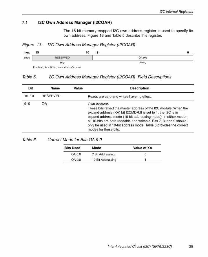
The 16-bit memory-mapped I2C own address register is used to specify itsown address. Figure 13 and Table 5 describe this register.
Figure 13. I2C Own Address Manager Register (I2COAR)
Table 5. 2C Own Address Manager Register (I2COAR) Field Descriptions
Table 6. Correct Mode for Bits OA.9:0
hex 15 10 9 0
0x00 RESERVED OA.9:0
R-0 RW-0
R = Read, W = Write, –n = Value after reset
Bit Name Value Description
15–10 RESERVED Reads are zero and writes have no effect.
9–0 OA Own AddressThese bits reflect the master address of the I2C module. When the expand address (XA) bit I2CMDR.8 is set to 1, the I2C is in expand address mode (10-bit addressing mode). In either mode, all 10-bits are both readable and writable. Bits 7, 8, and 9 should only be used in 10-bit address mode. Table 6 provides the correct modes for these bits.
Bits Used Mode Value of XA
OA.6:0 7 Bit Addressing 0
OA.9:0 10 Bit Addressing 1
Inter-Integrated Circuit (I2C) (SPNU223C) 25

I2C Internal Registers
7.2 I2C Interrupt Mask Register (I2CIMR)
The 7-bit memory mapped I2C interrupt mask register is used by the TMS470to enable/disable the interrupts. Figure 14 and Table 7 describe this register.
Figure 14. I2C Interrupt Mask Register (I2CIMR)
hex 15 7 6 5 4 3 2 1 0
0x04 RESERVEDAASEN
SCDEN
TXRDYEN RXRDYRN ARDYEN NACKEN ALEN
R-0 RW-0 RW-0 RW-0 RW-0 RW-0 RW-0 RW-0
R = Read, W = Write, –n = Value after reset
Table 7. I2C Interrupt Mask Register (I2CIMR) Field Descriptions
Bit Name Value Description
15–7 RESERVED Reads are zero and writes have no effect.
6 AASEN Address As Slave Interrupt Enable
0 The AASEN interrupt is disabled.
1 The AASEN interrupt is enabled.
5 SCDEN Stop Condition Interrupt Enable
0 The SCDEN interrupt is disabled.
1 The SCDEN interrupt is enabled.
4 TXRDYEN Transmit Data Ready Interrupt Enable
0 The TXRDYEN interrupt is disabled.
1 The TXRDYEN interrupt is enabled.
3 RXRDYEN Receive Data Ready Interrupt Enable
0 The RXRDYEN interrupt is disabled.
1 The RXRDYEN interrupt is enabled.
2 ARDYEN Register Access Ready Interrupt Enable
0 The ARDYEN interrupt is disabled.
1 The ARDYEN interrupt is enabled.
26

I2C Internal Registers
1 NACKEN No Acknowledgement Interrupt Enable
0 The NACKEN interrupt is disabled.
1 The NACKEN interrupt is enabled.
0 ALEN Arbitration Lost Interrupt Enable
0 The ALEN interrupt is disabled.
1 The ALEN interrupt is enabled.
Table 7. I2C Interrupt Mask Register (I2CIMR) Field Descriptions (Continued)
Inter-Integrated Circuit (I2C) (SPNU223C) 27
I2C Internal Registers
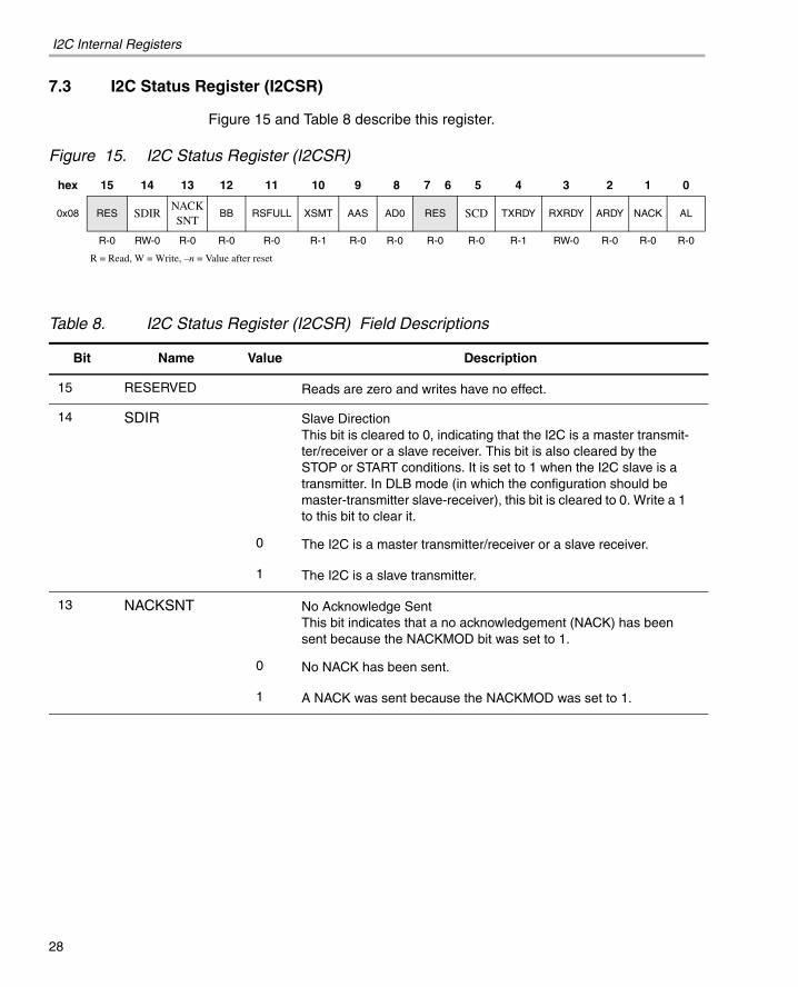
7.3 I2C Status Register (I2CSR)
Figure 15 and Table 8 describe this register.
Figure 15. I2C Status Register (I2CSR)
hex 15 14 13 12 11 10 9 8 7 6 5 4 3 2 1 0
0x08 RES SDIRNACKSNT
BB RSFULL XSMT AAS AD0 RES SCD TXRDY RXRDY ARDY NACK AL
R-0 RW-0 R-0 R-0 R-0 R-1 R-0 R-0 R-0 R-0 R-1 RW-0 R-0 R-0 R-0
R = Read, W = Write, –n = Value after reset
Table 8. I2C Status Register (I2CSR) Field Descriptions
Bit Name Value Description
15 RESERVED Reads are zero and writes have no effect.
14 SDIR Slave DirectionThis bit is cleared to 0, indicating that the I2C is a master transmit-ter/receiver or a slave receiver. This bit is also cleared by the STOP or START conditions. It is set to 1 when the I2C slave is a transmitter. In DLB mode (in which the configuration should be master-transmitter slave-receiver), this bit is cleared to 0. Write a 1 to this bit to clear it.
0 The I2C is a master transmitter/receiver or a slave receiver.
1 The I2C is a slave transmitter.
13 NACKSNT No Acknowledge SentThis bit indicates that a no acknowledgement (NACK) has been sent because the NACKMOD bit was set to 1.
0 No NACK has been sent.
1 A NACK was sent because the NACKMOD was set to 1.
28

I2C Internal Registers
12 BB Bus BusyThis bit indicates the state of the serial bus. On reception of a START condition or a low state on I2CSCL, the device sets BB = 1. BB is cleared to 0 after the reception of a STOP condition. In the MASTER mode, BB is controlled by software. On versions 1.x and earlier of the I2C, the only way to clear BB from software is by writ-ing a one to this bit. It should also be noted that on these versions, resetting nIRS will not clear BB. To start a transmission with a START condition, MST, TRX and STT must be set to 1. To end a transmission with a STOP condition, STP must be set to 1. When BB = 1 and STT = 1, a restart condition is generated.
0 The bus is free.
1 The bus is busy.
11 RSFULL Receiver Shift FullThis bit indicates whether the receiver has experienced overrun. Overrun occurs when the receive shift register is full and I2CDRR has not been read since the receive shift register to I2CDRR transfer. The contents of I2CDRR are not lost. The I2C core logic is holding for I2CDRR read access. This bit is also set when, in master-repeat-mode, the I2C receives a byte of data. There is no difference between RXRDY and RSFULL in this case. The I2C master will not continue the transfer as long as the received data is in the I2CDRR or receive shift register. RSFULL is cleared when reading the I2CDRR, resetting the I2C (IRS_=0), or resetting the device.
0 No overrun has occurred.
1 An overrun has occurred.
10 XSMT Transmit Shift Empty NotThis bit indicates whether the transmitter has experienced under-flow. Underflow occurs when the transmit shift register is empty and I2CDXR has not been loaded since the last I2CDXR to trans-mit shift register transfer. The I2C core logic is waiting for I2CDXR write access.
XMSTn is cleared when an underflow condition occurs. XMSTn is set by writing data to the I2CDXR register, by resetting the I2C block(IRS=0), or by resetting the device.
0 An underflow has occurred.
1 No underflow has occurred.
Table 8. I2C Status Register (I2CSR) Field Descriptions (Continued)
Inter-Integrated Circuit (I2C) (SPNU223C) 29
I2C Internal Registers
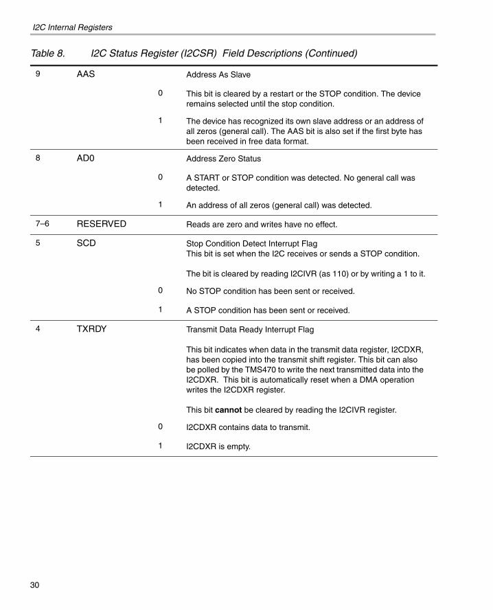
9 AAS Address As Slave
0 This bit is cleared by a restart or the STOP condition. The device remains selected until the stop condition.
1 The device has recognized its own slave address or an address of all zeros (general call). The AAS bit is also set if the first byte has been received in free data format.
8 AD0 Address Zero Status
0 A START or STOP condition was detected. No general call was detected.
1 An address of all zeros (general call) was detected.
7–6 RESERVED Reads are zero and writes have no effect.
5 SCD Stop Condition Detect Interrupt FlagThis bit is set when the I2C receives or sends a STOP condition.
The bit is cleared by reading I2CIVR (as 110) or by writing a 1 to it.
0 No STOP condition has been sent or received.
1 A STOP condition has been sent or received.
4 TXRDY Transmit Data Ready Interrupt Flag
This bit indicates when data in the transmit data register, I2CDXR, has been copied into the transmit shift register. This bit can also be polled by the TMS470 to write the next transmitted data into the I2CDXR. This bit is automatically reset when a DMA operation writes the I2CDXR register.
This bit cannot be cleared by reading the I2CIVR register.
0 I2CDXR contains data to transmit.
1 I2CDXR is empty.
Table 8. I2C Status Register (I2CSR) Field Descriptions (Continued)
30

I2C Internal Registers
3 RXRDY Receive Data Ready Interrupt FlagIndicates when the data in the receive shift register has been cop-ied into the data receive register (I2CDRR). This bit is cleared to 0 when the I2CDRR is read. This bit can also be polled by the TMS470 to read the received data in the I2CDRR.
This bit cannot be cleared by reading the I2CIVR register.
0 The I2CDRR has been read.
1 The received data has been written into the I2CDRR.
2 ARDY Register Access Ready Interrupt FlagThis bit indicates when the previously programmed address, data and command has been performed and status bit has been updated. The flag is used by the TMS470 to let it know that the I2C registers are ready to be accessed again. When RM=0, ARDY is set when I2CCNT is passed 0 if STP register bit has not been set. When RM=1, ARDY is set at each bytes end. When FDF is 0, ARDY is asserted after the ACK for the slave address. When FDF is 1, there is no slave address or ACK. Therefore, ARDY is asserted after sending the start condition.
This bit cannot be cleared by reading the I2CIVR register. It can be cleared by writing a 1 to it.
0 Nonrepeat mode, (RM = 0): I2C registers are not ready to be accessed. Repeat mode (RM = 1): I2C registers are not ready to be accessed.
1 Nonrepeat mode, (RM = 0): ICCNT passes 0 (if STP bit has not been set).Repeat mode (RM = 1): The end of each byte was transmitted from I2CDXR.
1 NACK No Acknowledgement InterruptThis bit indicates when the master I2C does not receive an acknowledgement from the receiver. This bit is set only when the I2C has received a no-acknowledge in master mode. In master start byte mode, the first byte (address of all zeroes) receives a NACK but does not clear the stop bit.
0 An acknowledge was detected.
1 No Acknowledge was detected or the I2C is operating in the gen-eral call, even though an Acknowledgement was received. This value clears the STP bit.
Table 8. I2C Status Register (I2CSR) Field Descriptions (Continued)
Inter-Integrated Circuit (I2C) (SPNU223C) 31
I2C Internal Registers
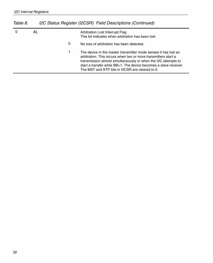
0 AL Arbitration Lost Interrupt FlagThis bit indicates when arbitration has been lost.
0 No loss of arbitration has been detected.
1 The device in the master transmitter mode senses it has lost an arbitration. This occurs when two or more transmitters start a transmission almost simultaneously or when the I2C attempts to start a transfer while BB=1. The device becomes a slave receiver. The MST and STP bits in I2CSR are cleared to 0.
Table 8. I2C Status Register (I2CSR) Field Descriptions (Continued)
32

I2C Internal Registers
7.4 I2C Clock Divider Low Register (I2CCKL)
The I2C clock divider low register is a 16-bit memory mapped register usedto divide the master clock down to obtain the I2C serial clock low time. Figure16 and Table 9 describe this register.
Figure 16. I2C Clock Divider Low Register (I2CCKL)
Table 9. I2C Clock Divider Low Register (I2CCKL) Field Descriptions
hex 15 0
0x0C CLKL.15:0
RW-0
R = Read, W = Write, –n = Value after reset
Bit Name Value Description
15–0 CLKL Low Time Clock Division FactorUsed to divide down the module clock to create the low time por-tion of the master clock signal that will appear on the SCL pin.:
(EQ 4)
where d is the value that depends on the I2CPSC (see Section 1.3).
LowTime I2CCLKL d+ModuleClockFrequency----------------------------------------------------------------⎝ ⎠⎛ ⎞=
Inter-Integrated Circuit (I2C) (SPNU223C) 33
I2C Internal Registers
7.5 I2C Clock Control High Register (I2CCKH)
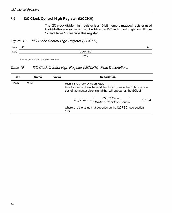
The I2C clock divider high register is a 16-bit memory mapped register usedto divide the master clock down to obtain the I2C serial clock high time. Figure17 and Table 10 describe this register.
Figure 17. I2C Clock Control High Register (I2CCKH)
Table 10. I2C Clock Control High Register (I2CCKH) Field Descriptions
hex 15 0
0x10 CLKH.15:0
RW-0
R = Read, W = Write, –n = Value after reset
Bit Name Value Description
15–0 CLKH High Time Clock Division FactorUsed to divide down the module clock to create the high time por-tion of the master clock signal that will appear on the SCL pin.
(EQ 5)
where d is the value that depends on the I2CPSC (see section 1.3).
HighTime I2CCLKH d+ModuleClockFrequency----------------------------------------------------------------⎝ ⎠⎛ ⎞=
34

I2C Internal Registers
7.6 I2C Data Count Register (I2CCNT)
The I2C data count register is a 16-bit memory mapped register used to countreceived or transmitted data bytes. This register is also used to generate theSTOP condition which terminates the transfer after the counter reaches zero.Figure 18 and Table 11 describe this register.
Figure 18. I2C Data Count Register (I2CCNT)
Table 11. I2C Data Count Register (I2CCNT) Field Descriptions
hex 15 0
0x14 CNT.15:0
RW-0
R = Read, W = Write, –n = Value after reset
Bit Name Value Description
15–0 CNT Data CounterThis down counter is used to generate a STOP condition if a STOP condition is specified (STP=1). Note that ICCNT is a don’t care when RM is set to 1.
0000h The data counter is 65536.
Inter-Integrated Circuit (I2C) (SPNU223C) 35

I2C Internal Registers
7.7 I2C Data Receive Register (I2CDRR)
The I2C data receive register is a 16-bit memory mapped register used by theTMS470 to read the received data. Figure 19 and Table 12 describe thisregister.
Figure 19. I2C Data Receive Register (I2CDRR)
Table 12. I2C Data Receive Register (I2CDRR) Field Descriptions
hex 15 8 7 0
0x18 RESERVED DATARX.7:0
R-0 R-0
R = Read, C = Clear, –n = Value after reset
Bit Name Value Description
15–8 RESERVED Reads are zero and writes have no effect.
7–0 DATARX Receive DataA read to this register clears the RXRDY bit and clears code 0x04 from the I2CIVR register.
36
I2C Internal Registers
7.8 I2C Slave Address Register (I2CSAR)
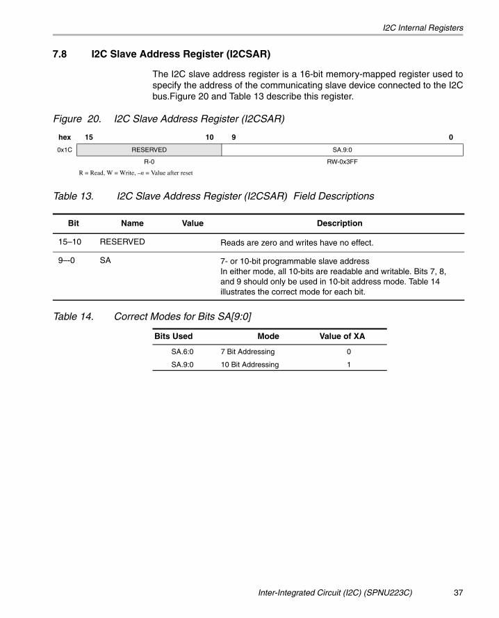
The I2C slave address register is a 16-bit memory-mapped register used tospecify the address of the communicating slave device connected to the I2Cbus.Figure 20 and Table 13 describe this register.
Figure 20. I2C Slave Address Register (I2CSAR)
Table 13. I2C Slave Address Register (I2CSAR) Field Descriptions
Table 14. Correct Modes for Bits SA[9:0]
hex 15 10 9 0
0x1C RESERVED SA.9:0
R-0 RW-0x3FF
R = Read, W = Write, –n = Value after reset
Bit Name Value Description
15–10 RESERVED Reads are zero and writes have no effect.
9–-0 SA 7- or 10-bit programmable slave addressIn either mode, all 10-bits are readable and writable. Bits 7, 8, and 9 should only be used in 10-bit address mode. Table 14 illustrates the correct mode for each bit.
Bits Used Mode Value of XA
SA.6:0 7 Bit Addressing 0
SA.9:0 10 Bit Addressing 1
Inter-Integrated Circuit (I2C) (SPNU223C) 37
I2C Internal Registers
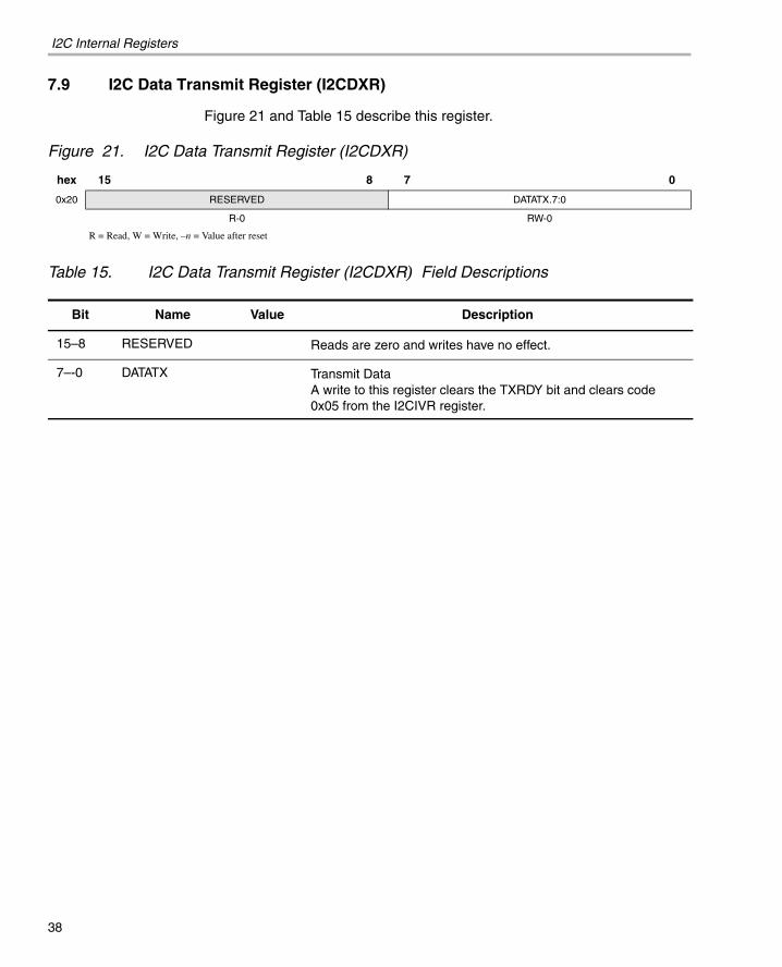
7.9 I2C Data Transmit Register (I2CDXR)
Figure 21 and Table 15 describe this register.
Figure 21. I2C Data Transmit Register (I2CDXR)
Table 15. I2C Data Transmit Register (I2CDXR) Field Descriptions
hex 15 8 7 0
0x20 RESERVED DATATX.7:0
R-0 RW-0
R = Read, W = Write, –n = Value after reset
Bit Name Value Description
15–8 RESERVED Reads are zero and writes have no effect.
7–-0 DATATX Transmit DataA write to this register clears the TXRDY bit and clears code 0x05 from the I2CIVR register.
38
I2C Internal Registers
7.10 I2C Mode Register (I2CMDR)
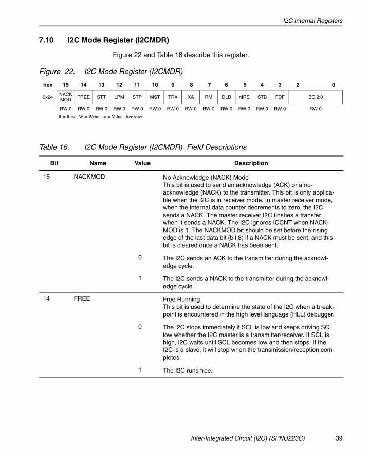
Figure 22 and Table 16 describe this register.
Figure 22. I2C Mode Register (I2CMDR)
hex 15 14 13 12 11 10 9 8 7 6 5 4 3 2 0
0x24 NACKMOD FREE STT LPM STP MST TRX XA RM DLB nIRS STB FDF BC.2:0
RW-0 RW-0 RW-0 RW-0 RW-0 RW-0 RW-0 RW-0 RW-0 RW-0 RW-0 RW-0 RW-0 RW-0
R = Read, W = Write, –n = Value after reset
Table 16. I2C Mode Register (I2CMDR) Field Descriptions
Bit Name Value Description
15 NACKMOD No Acknowledge (NACK) ModeThis bit is used to send an acknowledge (ACK) or a no-acknowledge (NACK) to the transmitter. This bit is only applica-ble when the I2C is in receiver mode. In master receiver mode, when the internal data counter decrements to zero, the I2C sends a NACK. The master receiver I2C finshes a transfer when it sends a NACK. The I2C ignores ICCNT when NACK-MOD is 1. The NACKMOD bit should be set before the rising edge of the last data bit (bit 8) if a NACK must be sent, and this bit is cleared once a NACK has been sent.
0 The I2C sends an ACK to the transmitter during the acknowl-edge cycle.
1 The I2C sends a NACK to the transmitter during the acknowl-edge cycle.
14 FREE Free Running This bit is used to determine the state of the I2C when a break-point is encountered in the high level language (HLL) debugger.
0 The I2C stops immediately if SCL is low and keeps driving SCL low whether the I2C master is a transmitter/receiver. If SCL is high, I2C waits until SCL becomes low and then stops. If the I2C is a slave, it will stop when the transmission/reception com-pletes.
1 The I2C runs free.
Inter-Integrated Circuit (I2C) (SPNU223C) 39

I2C Internal Registers
13 STT Start ConditionThe start condition bit works with the STP bit (master only mode). The STT and STP bits are configured to generate differ-ent transfer formats (see Table 17). Note that the STT and STP bits can be used to terminate the repeat mode. This bit takes one I2C cycle to set.
0 The STT is reset to 0 by the hardware after the START condi-tion has been generated.
1 STT is set to 1 by the TMS470 to generate a START condition. In master mode, setting STT to 1 generates a START condition. In slave mode, setting STT to 1 enables the I2C.
12 LPM Low Power ModeWhen this bit is active, the I2C module enters the power-down state and disables the internal clocks to the I2C module. This is the last bit set when the I2C module enters low-power mode. It is also the first bit written to when powering up the module.
0 I2C is not in low power mode.
1 I2C module is in low-power mode.
11 STP Stop ConditionThe stop condition bit works with the STT bit (master only mode). The STT and STP bits are configured to generate differ-ent transfer formats (see Table 17). Note that the STT and STP bits can be used to terminate the repeat mode. This bit takes one I2C cycle to set.
0 STP is reset to 0 by the hardware after the STOP condition has been generated. The STOP condition is generated when ICCNT passes 0.
1 STP is set to 1 by the TMS470 to generate a STOP condition.
10 MST Master/Slave Mode BitThis bit determines whether the module will operate in master or slave mode; see Table 18. This bit is cleared when the I2C master detects a STOP condition.
0 The module is in the slave mode and the clock is received from the master device
1 The module is in the master mode and it generates the clock. The MST bit works in conjunction with the TRX bit to determine the direction of data transmission of the I2C.
Table 16. I2C Mode Register (I2CMDR) Field Descriptions
40

I2C Internal Registers
9 TRX Transmit/Receive BitThis bit determines the direction of data transmission of the I2C module. See Table 18.
0 The module is in the receive mode and data on the SDA line is shifted into the data register I2CDRR
1 The module is in the transmit mode and the data in the I2CDXR is shifted out on the SDA line
8 XA Expand Address Enable BitThis bit controls the addressing mode. When XA is set to 1, the I2C does not support the combined format in master mode operations. However, the I2C will acknowledge and support the formats when configured as a slave. Read and write operations are also supported, but without the combined format using the repeated start condition).
0 The mode is set to 7-bit addressing mode (normal address mode).
1 The mode is set to 10-bit addressing mode (expanded address mode).
7 RM Repeat Mode Enable BitThis bit is a don’t care if the module is configured in slave mode (MST = 0); see Table 17. Each time a byte of data is received, the user should decide whether or not to continue receiving more data.
0 The mode is not in repeat mode.
1‘ In repeat mode, data is continuously transmitted out of the ICDXR until the STP bit is set to 1 regardless of ICCNT value. See Table 17 for module conditions.
6 DLB Digital Loop Back Enable BitThis bit disables or enables the digital loopback mode of the I2C.
0 Digital loop back mode is disabled.
1 Digital loop back mode is enabled. In digital loop back mode, data transmitted out of the I2CDXR will be received in the I2CDRR after
cycles via an internal path. The address of the I2COAR is out-put on SDA.
Table 16. I2C Mode Register (I2CMDR) Field Descriptions
SYSCLKFrequencyICLKofI2cModuleFrequency-----------------------------------------------------------------------------⎝ ⎠⎛ ⎞ 8⋅
Inter-Integrated Circuit (I2C) (SPNU223C) 41

I2C Internal Registers
5 nIRS I2C Reset Enable BitWhen set to zero, this bit will place all status registers in this module to their default state.
However, on versions 1.x and earlier of the I2C, when in master mode, resetting the nIRS will not clear the BB bit. The only way of clearing BB by software is by writing a 1 to the bit.
Note: Resetting nIRSResetting nIRS during a data transfer can hang the I2C bus.
0 I2C is in reset.
1 I2C is out of reset.
4 STB Start Byte Mode Enable BitThis bit places the module into start byte mode. This byte is generated within the start procedure and is used when polling is the method to detect activity of the I2C bus. A NACK will be generated by the slave on the first byte. The value of the START byte is 00000001. (In master only mode, zeroes represent the address and the one represents the NACK)
0 The module is not in START byte mode.
1 The module is in START byte mode.
3 FDF Free Data Format Enable BitThis bit onfigures the module to operate in free data format mode (see Table 18) in both master and slave modes. When FDF is 0, ARDY is asserted after ACK for the slave address. When FDF is 1, there is no slave address or ACK. Therefore, ARDY is asserted after sending the start condition.
0 The module is not in free data format mode.
1 The module is in free data format mode.
Table 16. I2C Mode Register (I2CMDR) Field Descriptions
42
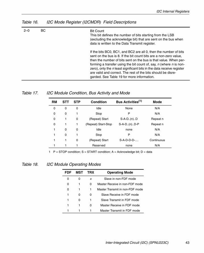
I2C Internal Registers
Table 17. I2C Module Condition, Bus Activity and Mode
1 P = STOP condition; S = START condition; A = Acknowledge bit; D = data
Table 18. I2C Module Operating Modes
2–0 BC Bit CountThis bit defines the number of bits starting from the LSB (excluding the acknowledge bit) that are sent on the bus when data is written to the Data Transmit register.
If the bits BC0, BC1, and BC2 are all 0, then the number of bits sent on the bus is 8. If the bit count bits are a non-zero value, then the number of bits sent on the bus is that value. When per-forming a transfer using the bit count of, say, n (where n is non-zero), only the n least significant bits in the data receive register are valid and correct. The rest of the bits should be disre-garded. See Table 19 for more information.
RM STT STP Condition Bus Activities(1) Mode
0 0 0 Idle None N/A
0 0 1 Stop P N/A
0 1 0 (Repeat) Start S-A-D..(n)..D Repeat n
0 1 1 (Repeat) Start-Stop S-A-D..(n)..D-P Repeat n
1 0 0 Idle none N/A
1 0 1 Stop P N/A
1 1 0 (Repeat) Start S-A-D-D-D-.... Continuous
1 1 1 Reserved none N/A
FDF MST TRX Operating Mode
0 0 x Slave in non-FDF mode
0 1 0 Master Receive in non-FDF mode
0 1 1 Master Transmit in non-FDF mode
1 0 0 Slave Receive in FDF mode
1 0 1 Slave Transmit in FDF mode
1 1 0 Master Receive in FDF mode
1 1 1 Master Transmit in FDF mode
Table 16. I2C Mode Register (I2CMDR) Field Descriptions
Inter-Integrated Circuit (I2C) (SPNU223C) 43
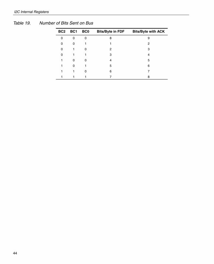
I2C Internal Registers
Table 19. Number of Bits Sent on Bus
BC2 BC1 BC0 Bits/Byte in FDF Bits/Byte with ACK
0 0 0 8 9
0 0 1 1 2
0 1 0 2 3
0 1 1 3 4
1 0 0 4 5
1 0 1 5 6
1 1 0 6 7
1 1 1 7 8
44
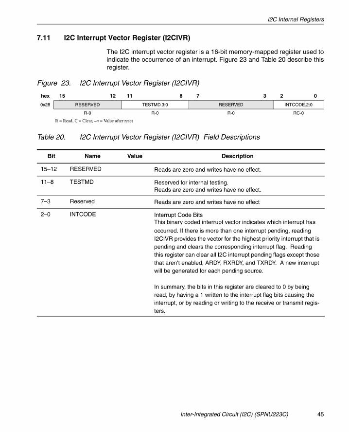
I2C Internal Registers
7.11 I2C Interrupt Vector Register (I2CIVR)
The I2C interrupt vector register is a 16-bit memory-mapped register used toindicate the occurrence of an interrupt. Figure 23 and Table 20 describe thisregister.
Figure 23. I2C Interrupt Vector Register (I2CIVR)
Table 20. I2C Interrupt Vector Register (I2CIVR) Field Descriptions
hex 15 12 11 8 7 3 2 0
0x28 RESERVED TESTMD.3:0 RESERVED INTCODE.2:0
R-0 R-0 R-0 RC-0
R = Read, C = Clear, –n = Value after reset
Bit Name Value Description
15–12 RESERVED Reads are zero and writes have no effect.
11–8 TESTMD Reserved for internal testing.Reads are zero and writes have no effect.
7–3 Reserved Reads are zero and writes have no effect
2–0 INTCODE Interrupt Code BitsThis binary coded interrupt vector indicates which interrupt has
occurred. If there is more than one interrupt pending, reading I2CIVR provides the vector for the highest priority interrupt that is pending and clears the corresponding interrupt flag. Reading this register can clear all I2C interrupt pending flags except those that aren't enabled, ARDY, RXRDY, and TXRDY. A new interrupt will be generated for each pending source.
In summary, the bits in this register are cleared to 0 by being read, by having a 1 written to the interrupt flag bits causing the interrupt, or by reading or writing to the receive or transmit regis-ters.
Inter-Integrated Circuit (I2C) (SPNU223C) 45
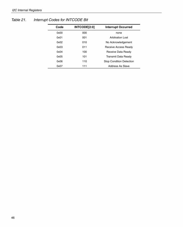
I2C Internal Registers
Table 21. Interrupt Codes for INTCODE Bit
Code INTCODE[2:0] Interrupt Occurred
0x00 000 none
0x01 001 Arbitration Lost
0x02 010 No Acknowledgement
0x03 011 Receive Access Ready
0x04 100 Receive Data Ready
0x05 101 Transmit Data Ready
0x06 110 Stop Condition Detection
0x07 111 Address As Slave
46

I2C Internal Registers
7.12 I2C Extended Mode Register (I2CEMDR)
The I2C extended mode register is a 16-bit memory-mapped register used toestablish compatibility between previously released versions of the I2Cmodule. Figure 24 and Table 22 describe this register.
Figure 24. I2C Extended Mode Register (I2CEMDR)
Table 22. I2C Extended Mode Register (I2CEMDR) Field Descriptions
hex 15 1 0
0x2C RESERVED BCM
R-0 RW-0
R = Read, W = Write, –n = Value after reset
Bit Name Value Description
15–1 RESERVED Reads are zero and writes have no effect.
0 BCM Backwards Compatibility ModeWhen set to 1, the I2C is compatible with previous versions of the I2C. This means the TXRDY interrupt is generated in slave-transmit mode when TXRDY is set and the I2C needs more data to transmit. This behavior causes an extra TXRDY inter-rupt to be generated because the I2C recognizes the end of transfer after generating an interrupt for the next byte of data.
When BCM is 0, the TXRDY interrupt in slave-transmit mode is generated when XSMT = 1. In this case, the I2C generates an interrupt for the next byte after receiving the ACK from previous data. The setting of this bit only applies to slave transmit mode.
0 The I2C is not in compatibility mode.
1 The I2C is in compatibility mode.
Inter-Integrated Circuit (I2C) (SPNU223C) 47

I2C Internal Registers
7.13 I2C Prescale Register (I2CPSC)
The I2C prescaler register is a 16-bit memory-mapped register used fordividing down the ICLK to obtain a module clock frequency between 6.7 MHzand 13.3 MHz. Figure 25 and Table 23 describe this register.
Figure 25. I2C Prescale Register (I2CPSC)
Table 23. I2C Prescale Register (I2CPSC) Field Descriptions
hex 15 8 7 0
0x30 RESERVED PSC.7:0
R-0 RW-0
R = Read, W = Write, –n = Value after reset
Bit Name Value Description
15–8 RESERVED Reads are zero and writes have no effect.
7–0 PSC Prescale RegisterI2CPSC affects the dividing value on the rising edge on nIRS. The value of the I2CPSC is transferred to the internal register, which controls the I2C clock frequency on the rising edge of nIRS. When nIRS is 0, the frequency of the I2C clock is unchanged even if I2CPSC is updated. See Section 1.3 for more information.
48

I2C Internal Registers
7.14 I2C Data Direction Register (I2CDIR)
This register contains the control register for the direction and functionality ofthe two I2C pins SDA and SCL. Figure 26 and Table 24 describe this register.
Figure 26. I2C Data Direction Register (I2CDIR)
hex 15 6 5 4 3 2 1 0
0x34 RESERVED TXDMAEN RXDMAEN SDAFUNC SCLFUNC SDADIR SCLDIR
R-0 RW-0 RW-0 RW-0 RW-0 RW-0 RW-0
R = Read, W = Write, –n = Value after reset
Table 24. I2C Data Direction Register (I2CDIR) Field Descriptions
Bit Name Value Description
15–6 RESERVED Reads are zero and writes have no effect.
5 TXDMAEN Transmitter DMA EnableThis bit controls the transmit DMA request pin to the system. When this bit is a 1, the DMA is enabled and the DMA can occur. When this bit is a 0, the DMA request is disabled.
Writing a 1 to this bit will send a TXDMA request to the DMA module if SDAFUNC and SCLFUNC are also set to 1.
0 The transmit DMA is disabled.
1 The transmit DMA is enabled.
4 RXDMAEN Receive DMA EnableThis bit controls the receive DMA request pin to the system. When this bit is 1, the DMA is enabled and the DMA can occur. When this bit is a 0, the DMA request is disabled.
0 The receive DMA is disabled.
1 The receive DMA is enabled.
3 SDAFUNC SDA Pin Function This bit controls whether the SDA pin functions as an I2C pin or as an I/O pin. When this bit is 0, the SDA pin functions as an I/O pin controlled by the values in the SDAOUT and SDADIR. When this bit is set to 1, it becomes the I2C SDA function pin. The values in SDAOUT and SDADIR will remain unchanged but they will be ignored.
0 The SDA pin is an I/O pin.
1 The SDA pin is an I2C pin.
Inter-Integrated Circuit (I2C) (SPNU223C) 49

I2C Internal Registers
2 SCLFUNC SCL Pin Function This bit controls whether the SCL pin functions as an I2C pin or as an I/O pin. When this bit is 0, the SCL pin functions as an I/O pin controlled by the values in the SCLOUT and SCLDIR. When this bit is set to 1, it becomes the I2C SCL function pin. The values in SCLOUT and SCLDIR will remain unchanged but they will be ignored.
0 The SCL pin is an I/O pin. Bit SCLDIR determines whether it is an input pin or an output pin.
1 The SCL pin is an I2C pin.
1 SDADIR SDA Direction Pin This bit controls the direction of the SDA pin when it is used as a general purpose I/O pin and SDAFUNC = 0. When SDAFUNC = 1, the bit is still readable and writable but the bit will have no effect on the pin.
0 The pin is an input.
1 The pin is an output.
0 SCLDIR SCL DirectionThis bit controls the direction of the SCL pin when it is used as a general purpose I/O pin and SCLFUNC = 0. When SCLFUNC = 1, the bit is still readable and writable but the bit will have no effect on the pin.
0 The pin is an input.
1 The pin is an output.
Table 24. I2C Data Direction Register (I2CDIR) Field Descriptions (Continued)
50
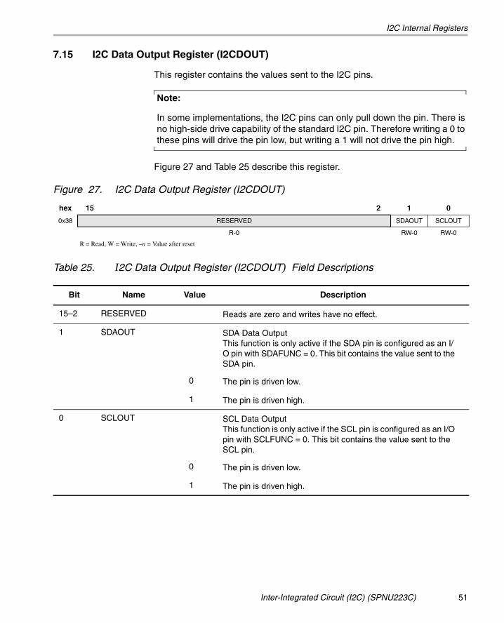
I2C Internal Registers
7.15 I2C Data Output Register (I2CDOUT)
This register contains the values sent to the I2C pins.
Note:
In some implementations, the I2C pins can only pull down the pin. There isno high-side drive capability of the standard I2C pin. Therefore writing a 0 tothese pins will drive the pin low, but writing a 1 will not drive the pin high.
Figure 27 and Table 25 describe this register.
Figure 27. I2C Data Output Register (I2CDOUT)
Table 25. I2C Data Output Register (I2CDOUT) Field Descriptions
hex 15 2 1 0
0x38 RESERVED SDAOUT SCLOUT
R-0 RW-0 RW-0
R = Read, W = Write, –n = Value after reset
Bit Name Value Description
15–2 RESERVED Reads are zero and writes have no effect.
1 SDAOUT SDA Data OutputThis function is only active if the SDA pin is configured as an I/O pin with SDAFUNC = 0. This bit contains the value sent to the SDA pin.
0 The pin is driven low.
1 The pin is driven high.
0 SCLOUT SCL Data OutputThis function is only active if the SCL pin is configured as an I/O pin with SCLFUNC = 0. This bit contains the value sent to the SCL pin.
0 The pin is driven low.
1 The pin is driven high.
Inter-Integrated Circuit (I2C) (SPNU223C) 51

I2C Internal Registers
7.16 I2C Data Input Register (I2CDIN)
Figure 28 and Table 26 describe this register.
Figure 28. I2C Data Input Register (I2CDIN)
Table 26. I2C Data Input Register (I2CDIN) Field Descriptions
hex 15 2 1 0
0x3C RESERVED SDAIN SCLIN
R-0 R-x R-x
R = Read, –x = Value after reset is indeterminate
Bit Name Value Description
15–2 RESERVED Reads are zero and writes have no effect.
1 SDAIN Serial Data InThe value of this bit reflects the value on the SDA pin.
0 SCLIN Serial Clock Data InThe value of this bit reflects the value on the SCL pin.
52
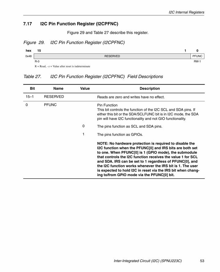
I2C Internal Registers
7.17 I2C Pin Function Register (I2CPFNC)
Figure 29 and Table 27 describe this register.
Figure 29. I2C Pin Function Register (I2CPFNC)
Table 27. I2C Pin Function Register (I2CPFNC) Field Descriptions
hex 15 1 0
0x48 RESERVED PFUNC
R-0 RW-1
R = Read, –x = Value after reset is indeterminate
Bit Name Value Description
15–1 RESERVED Reads are zero and writes have no effect.
0 PFUNC Pin FunctionThis bit controls the function of the I2C SCL and SDA pins. If either this bit or the SDA/SCLFUNC bit is in I2C mode, the SDA pin will have I2C functionality and not GIO functionality.
0 The pins function as SCL and SDA pins.
1 The pins function as GPIOs.
NOTE: No hardware protection is required to disable the I2C function when the PFUNC[0] and IRS bits are both set to one. When PFUNC[0] is 1 (GPIO mode), the submodule that controls the I2C function receives the value 1 for SCL and SDA. IRS can be set to 1 regardless of PFUNC[0], and the I2C function works whenever the IRS bit is 1. The user is expected to hold I2C in reset via the IRS bit when chang-ing to/from GPIO mode via the PFUNC[0] bit.
Inter-Integrated Circuit (I2C) (SPNU223C) 53
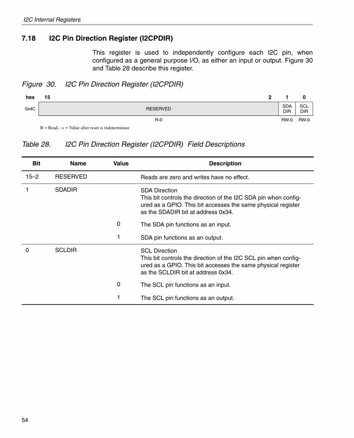
I2C Internal Registers
7.18 I2C Pin Direction Register (I2CPDIR)
This register is used to independently configure each I2C pin, whenconfigured as a general purpose I/O, as either an input or output. Figure 30and Table 28 describe this register.
Figure 30. I2C Pin Direction Register (I2CPDIR)
Table 28. I2C Pin Direction Register (I2CPDIR) Field Descriptions
hex 15 2 1 0
0x4C RESERVED SDA DIR
SCL DIR
R-0 RW-0 RW-0
R = Read, –x = Value after reset is indeterminate
Bit Name Value Description
15–2 RESERVED Reads are zero and writes have no effect.
1 SDADIR SDA DirectionThis bit controls the direction of the I2C SDA pin when config-ured as a GPIO. This bit accesses the same physical register as the SDADIR bit at address 0x34.
0 The SDA pin functions as an input.
1 SDA pin functions as an output.
0 SCLDIR SCL Direction This bit controls the direction of the I2C SCL pin when config-ured as a GPIO. This bit accesses the same physical register as the SCLDIR bit at address 0x34.
0 The SCL pin functions as an input.
1 The SCL pin functions as an output.
54
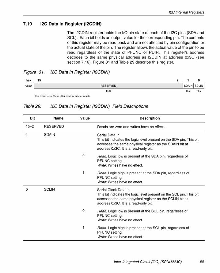
I2C Internal Registers
7.19 I2C Data In Register (I2CDIN)
The I2CDIN register holds the I/O pin state of each of the I2C pins (SDA andSCL). Each bit holds an output value for the corresponding pin. The contentsof this register may be read back and are not affected by pin configuration orthe actual state of the pin. The register allows the actual value of the pin to beread regardless of the state of PFUNC or PDIR. This register’s addressdecodes to the same physical address as I2CDIN at address 0x3C (seesection 7.16). Figure 31 and Table 29 describe this register.
Figure 31. I2C Data In Register (I2CDIN)
Table 29. I2C Data In Register (I2CDIN) Field Descriptions
hex 15 2 1 0
0x50 RESERVED SDAIN SCLIN
R-0 R-x R-x
R = Read, –x = Value after reset is indeterminate
Bit Name Value Description
15–2 RESERVED Reads are zero and writes have no effect.
1 SDAIN Serial Data InThis bit indicates the logic level present on the SDA pin. This bit accesses the same physical register as the SDAIN bit at address 0x3C. It is a read-only bit.
0 Read: Logic low is present at the SDA pin, regardless of PFUNC setting.Write: Writes have no effect.
1 Read: Logic high is present at the SDA pin, regardless of PFUNC setting.Write: Writes have no effect.
0 SCLIN Serial Clock Data InThis bit indicates the logic level present on the SCL pin. This bit accesses the same physical register as the SCLIN bit at address 0x3C. It is a read-only bit.
0 Read: Logic low is present at the SCL pin, regardless of PFUNC setting.Write: Writes have no effect.
1 Read: Logic high is present at the SCL pin, regardless of PFUNC setting.Write: Writes have no effect.
Inter-Integrated Circuit (I2C) (SPNU223C) 55

I2C Internal Registers
7.20 I2C Data Out Register (I2CDOUT)
The I2CDOUT register has one bit for each of the GPIO pins. Each bit holdsan output value for the corrsponding pin. The contents of this register may beread back and are not affected by pin configuration or by the actual state ofthe pin. The value in this register is driven out onto the GPIO pin only if thePFUNC bit in I2CPFNC is set to 1 (SDA and SCL function as GPIO) and alsothe corresponding bit in I2CDIR or I2CPDIR is set to 1 (Output). Thisregister’s address decodes to the same physical address as I2CDOUT ataddress 0x38 (see section 7.15). Figure 32 and Table 30 describe thisregister.
Figure 32. I2C Data Out Register (I2CDOUT)
Table 30. I2C Data Out Register (I2CDOUT) Field Descriptions
hex 15 2 1 0
0x54 RESERVED SDAOUT SCLOUT
R-0 RW-0 RW-0
R = Read, –x = Value after reset is indeterminate
Bit Name Value Description
15–2 RESERVED Reads are zero and writes have no effect.
1 SDAOUT Serial Data OutThis bit controls the level driven on the SDA pin when config-ured as GPIO output. This bit accesses the same physical reg-ister as the SDAOUT bit at address 0x38.
0 Reads: Reads return register values, not GPIO pin levels.Writes: The SDA pin is driven low.
1 Reads: Reads return register values, not GPIO pin levels.Writes: The SDA pin is driven high.
0 SCLIN Serial Clock Data OutThis bit controls the level driven on the SCL pin when config-ured as GPIO output. This bit accesses the same physical reg-ister as the SCLOUT bit at address 0x38.
0 Reads: Reads return register values, not GPIO pin levels.Writes: The SCL pin is driven low.
1 Reads: Reads return register values, not GPIO pin levels.Writes: The SCL pin is driven high.
56

I2C Internal Registers
7.21 I2C Data Set Register (I2CDSET)
The I2CDSET register is an alias of the I2CDOUT register. When written toat this address, writing a 1 to a bit sets the corresponding bit in I2CDOUT toa 1, while writing a 0 leaves it unchanged. Figure 33 and Table 31 describethis register.
Figure 33. I2C Data Set Register (I2CDSET)
Table 31. I2C Data Set Register (I2CDSET) Field Descriptions
hex 15 2 1 0
0x58 RESERVED SDASET SCLSET
R-0 RW-0 RW-0
R = Read, –x = Value after reset is indeterminate
Bit Name Value Description
15–2 RESERVED Reads are zero and writes have no effect.
1 SDASET Serial Data SetThis bit is used to set the SDA GPIO pin.
0 Reads: Reads are indeterminate.Writes: No effect occurs.
1 Reads: Reads are indeterminate.Writes: The SDASET bit is set to logic high.
0 SCLIN Serial Clock SetThis bit is used to set the SCL GPIO pin.
0 Reads: Reads are indeterminate.Writes: No effect occurs.
1 Reads: Reads are indeterminate.Writes: The SCLSET bit is set to logic high.
Inter-Integrated Circuit (I2C) (SPNU223C) 57
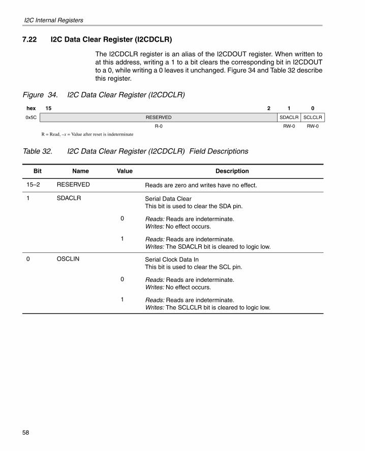
I2C Internal Registers
7.22 I2C Data Clear Register (I2CDCLR)
The I2CDCLR register is an alias of the I2CDOUT register. When written toat this address, writing a 1 to a bit clears the corresponding bit in I2CDOUTto a 0, while writing a 0 leaves it unchanged. Figure 34 and Table 32 describethis register.
Figure 34. I2C Data Clear Register (I2CDCLR)
Table 32. I2C Data Clear Register (I2CDCLR) Field Descriptions
hex 15 2 1 0
0x5C RESERVED SDACLR SCLCLR
R-0 RW-0 RW-0
R = Read, –x = Value after reset is indeterminate
Bit Name Value Description
15–2 RESERVED Reads are zero and writes have no effect.
1 SDACLR Serial Data ClearThis bit is used to clear the SDA pin.
0 Reads: Reads are indeterminate.Writes: No effect occurs.
1 Reads: Reads are indeterminate.Writes: The SDACLR bit is cleared to logic low.
0 OSCLIN Serial Clock Data InThis bit is used to clear the SCL pin.
0 Reads: Reads are indeterminate.Writes: No effect occurs.
1 Reads: Reads are indeterminate.Writes: The SCLCLR bit is cleared to logic low.
58

I2C Internal Registers
7.23 I2C Peripheral ID Register 1 (I2CPID1)
Figure 35 and Table 33 describe this register.
Figure 35. I2C Peripheral ID Register 1 (I2CPID1)
Table 33. I2C Peripheral ID Register 1 (I2CPID1) Field Descriptions
hex 15 8 7 0
0x64 CLASS REVISION
R-1 R-25h
R = Read, –x = Value after reset is indeterminate
Bit Name Value Description
15–8 CLASS Peripheral ClassThese bits identify the class of peripheral.
7–0 REVISION Revision Level of the I2CThese bits identify the revision level of the I2C.
Inter-Integrated Circuit (I2C) (SPNU223C) 59
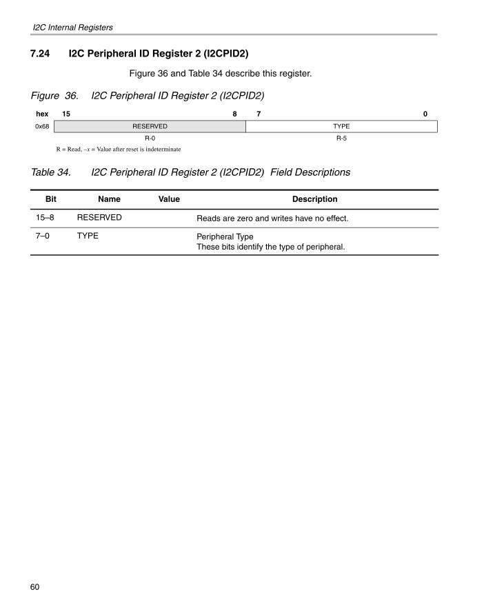
I2C Internal Registers
7.24 I2C Peripheral ID Register 2 (I2CPID2)
Figure 36 and Table 34 describe this register.
Figure 36. I2C Peripheral ID Register 2 (I2CPID2)
Table 34. I2C Peripheral ID Register 2 (I2CPID2) Field Descriptions
hex 15 8 7 0
0x68 RESERVED TYPE
R-0 R-5
R = Read, –x = Value after reset is indeterminate
Bit Name Value Description
15–8 RESERVED Reads are zero and writes have no effect.
7–0 TYPE Peripheral TypeThese bits identify the type of peripheral.
60