TMP105 data sheet - Texas Instruments · TMP105 0.1 Fm V+ GND A2 B2 C1 ALERT (Output) C2 A0 B1 A1...
22
Chip-Scale Package A1 B1 C1 A2 B2 C2 SDA SCL V+ GND ALERT A0 YZC LEAD- FREE 2 X 3 ARRAY (TOP VIEW) Note: Pin A1 is marked with a for Pb-free (YZC) 0 1,65 mm 1,50 mm 1,15 mm 1,00 mm (Bump Side Down) Diode Temp. Sensor DS A/D Converter OSC Control Logic Serial Interface Config. and Temp. Register TMP105 Temperature V+ SDA A1 C1 A2 C2 GND A0 SCL B1 B2 ALERT TMP105 www.ti.com SLLS648D – FEBRUARY 2005 – REVISED SEPTEMBER 2011 Digital Temperature Sensor with Two-Wire Interface Check for Samples: TMP105 1FEATURES DESCRIPTION 23• SUPPORTS 1.8V I 2 C™ BUS The TMP105 is a two-wire, serial output temperature • TWO ADDRESSES sensor available in a WCSP package. Requiring no • DIGITAL OUTPUT: Two-Wire Serial Interface external components, the TMP105 is capable of reading temperatures with a resolution of 0.0625°C. • RESOLUTION: 9- to 12-Bits, User-Selectable • ACCURACY: The TMP105 features a Two-Wire interface that is SMBus-compatible, with the TMP105 allowing up to – ±2.0°C (max) from –25°C to +85°C two devices on one bus. The TMP105 features an – ±3.0°C (max) from –40°C to +125°C SMBus Alert function. • LOW QUIESCENT CURRENT: The TMP105 is ideal for extended temperature 50μA, 1.5μA Standby measurement in a variety of communication, • NO POWER-UP SEQUENCE REQUIRED, I 2 C computer, consumer, environmental, industrial, and PULLUPS CAN BE ENABLED PRIOR TO V+ instrumentation applications. The TMP105 is specified for operation over a APPLICATIONS temperature range of –40°C to +125°C. • CELL PHONES • COMPUTER PERIPHERAL THERMAL PROTECTION • NOTEBOOK COMPUTERS • BATTERY MANAGEMENT • THERMOSTAT CONTROLS • ENVIRONMENTAL MONITORING AND HVAC 1 Please be aware that an important notice concerning availability, standard warranty, and use in critical applications of Texas Instruments semiconductor products and disclaimers thereto appears at the end of this data sheet. 2I 2 C is a trademark of NXP Semiconductors. 3All other trademarks are the property of their respective owners. PRODUCTION DATA information is current as of publication date. Copyright © 2005–2011, Texas Instruments Incorporated Products conform to specifications per the terms of the Texas Instruments standard warranty. Production processing does not necessarily include testing of all parameters.
Transcript of TMP105 data sheet - Texas Instruments · TMP105 0.1 Fm V+ GND A2 B2 C1 ALERT (Output) C2 A0 B1 A1...

Chip-Scale
Package
A1
B1
C1
A2
B2
C2
SDA
SCL
V+
GND
ALERT
A0
YZC LEAD- FREE
2 X 3 ARRAY
(TOP VIEW)
Note: Pin A1 is marked with a for Pb-free (YZC)0
1,65 mm
1,50 mm
1,15 mm
1,00 mm
(Bump Side Down)
Diode
Temp.
Sensor
DS
A/D
Converter
OSC
Control
Logic
Serial
Interface
Config.
and Temp.
Register
TMP105
Temperature
V+
SDAA1
C1
A2
C2
GND
A0
SCLB1 B2
ALERT
TMP105
www.ti.com SLLS648D –FEBRUARY 2005–REVISED SEPTEMBER 2011
Digital Temperature Sensorwith Two-Wire Interface
Check for Samples: TMP105
1FEATURESDESCRIPTION
23• SUPPORTS 1.8V I2C™ BUSThe TMP105 is a two-wire, serial output temperature• TWO ADDRESSESsensor available in a WCSP package. Requiring no
• DIGITAL OUTPUT: Two-Wire Serial Interface external components, the TMP105 is capable ofreading temperatures with a resolution of 0.0625°C.• RESOLUTION: 9- to 12-Bits, User-Selectable
• ACCURACY: The TMP105 features a Two-Wire interface that isSMBus-compatible, with the TMP105 allowing up to– ±2.0°C (max) from –25°C to +85°Ctwo devices on one bus. The TMP105 features an– ±3.0°C (max) from –40°C to +125°CSMBus Alert function.
• LOW QUIESCENT CURRENT:The TMP105 is ideal for extended temperature50μA, 1.5μA Standbymeasurement in a variety of communication,
• NO POWER-UP SEQUENCE REQUIRED, I2C computer, consumer, environmental, industrial, andPULLUPS CAN BE ENABLED PRIOR TO V+ instrumentation applications.
The TMP105 is specified for operation over aAPPLICATIONStemperature range of –40°C to +125°C.
• CELL PHONES• COMPUTER PERIPHERAL THERMAL
PROTECTION• NOTEBOOK COMPUTERS• BATTERY MANAGEMENT• THERMOSTAT CONTROLS• ENVIRONMENTAL MONITORING AND HVAC
1
Please be aware that an important notice concerning availability, standard warranty, and use in critical applications of TexasInstruments semiconductor products and disclaimers thereto appears at the end of this data sheet.
2I2C is a trademark of NXP Semiconductors.3All other trademarks are the property of their respective owners.
PRODUCTION DATA information is current as of publication date. Copyright © 2005–2011, Texas Instruments IncorporatedProducts conform to specifications per the terms of the TexasInstruments standard warranty. Production processing does notnecessarily include testing of all parameters.

A1
B1
C1
A2
B2
C2
SDA
SCL
V+
GND
ALERT
A0
WCSP-6 PACKAGE(TOP VIEW)
Note: Pin 1 is determined by orienting the package marking as indicated in the diagram.
(Bump Side Down)
TMP105
SLLS648D –FEBRUARY 2005–REVISED SEPTEMBER 2011 www.ti.com
This integrated circuit can be damaged by ESD. Texas Instruments recommends that all integrated circuits be handled withappropriate precautions. Failure to observe proper handling and installation procedures can cause damage.
ESD damage can range from subtle performance degradation to complete device failure. Precision integrated circuits may be moresusceptible to damage because very small parametric changes could cause the device not to meet its published specifications.
ORDERING INFORMATION (1)
PACKAGE PART NUMBER SYMBOL
Wafer chip-scale package (YZC) TMP105YZC EY
(1) For the most current package and ordering information, see the Package Option Addendum at the end of this document, or see theproduct folder at www.ti.com.
ABSOLUTE MAXIMUM RATINGS (1)
Power Supply, V+ 7.0V
Input Voltage (2) –0.5V to 7.0V
Input Current 10mA
Operating Temperature Range –55°C to +127°CStorage Temperature Range –60°C to +130°CJunction Temperature (TJ max) +150°CESD Rating: Human Body Model (HBM) (3) 2000V
Charged-Device Model (CDM) (4) 500V
Machine Model (MM) (5) 200V
(1) Stresses above these ratings may cause permanent damage. Exposure to absolute maximum conditions for extended periods maydegrade device reliability. These are stress ratings only, and functional operation of the device at these or any other conditions beyondthose specified is not implied.
(2) Input voltage rating applies to all TMP105 input voltages.(3) HBM testing has been tested to TI specifications JEDEC JESD22-A114C.01.(4) CDM testing has been tested to TI specifications JEDEC EIA/JESD22-A115A.(5) MM testing has been tested to TI specifications JEDEC JESD22-C101C.
PIN ASSIGNMENTS
2 Submit Documentation Feedback Copyright © 2005–2011, Texas Instruments Incorporated
Product Folder Link(s): TMP105

TMP105
www.ti.com SLLS648D –FEBRUARY 2005–REVISED SEPTEMBER 2011
ELECTRICAL CHARACTERISTICSAt TA = –40°C to +125°C, and V+ = 2.6V to 3.3V, unless otherwise noted.
TMP105PARAMETER CONDITION UNIT
MIN TYP MAX
TEMPERATURE INPUT
Range –40 +125 °C
Accuracy (Temperature Error) –25°C to +85°C ±0.5 ±2.0 °C
–40°C to +125°C ±1.0 ±3.0 °C
vs Supply 0.2 ±0.5 °C/V
Resolution (1) Selectable 0.0625 °C
DIGITAL INPUT/OUTPUT(SCL, SDA, ALERT)
Input Capacitance 3 pF
Input Logic Levels:
VIH 1.2 6.0 V
VIL –0.5 0.6 V
Leakage Input Current, IIN 0V ≤ VIN ≤ 6V 1 μA
Input Voltage Hysteresis SCL and SDA Pins 100 mV
Output Logic Levels:
VOL SDA IOL = 3mA 0 0.15 0.4 V
VOL ALERT IOL = 4mA 0 0.15 0.4 V
Resolution Selectable 9 to 12 Bits
Conversion Time 9-Bit 27.5 37.5 ms
10-Bit 55 75 ms
11-Bit 110 150 ms
12-Bit 220 300 ms
Timeout Time 25 54 74 ms
DIGITAL INPUT (A0)
Input Capacitance 3 pF
Input Logic Levels:
VIH 0.7 x (V+) (V+) + 0.5 V
VIL –0.5 0.3 x (V+) V
Leakage Input Current, IIN 0V ≤ VIN ≤ V+ 1 μA
POWER SUPPLY
Operating Range 2.6 3.3 V
Quiescent Current IQ Serial Bus Inactive 50 85 μA
Serial Bus Active, SCL Freq = 400kHz 100 μA
Shutdown Current ISD Serial Bus Inactive 1.5 3 μA
Serial Bus Active, SCL Freq = 400kHz 60 μA
TEMPERATURE RANGE
Specified Range –40 +125 °C
Operating Range –55 +127 °C
Thermal Resistance θJA 240 °C/W
(1) Specified for 12-bit resolution.
Copyright © 2005–2011, Texas Instruments Incorporated Submit Documentation Feedback 3
Product Folder Link(s): TMP105
Temperature ( C)°
I(
A)
mQ
-50 -25 0
100
80
60
40
20
0
25 50 75 100 125
V+ = 2.6V
Temperature ( C)°
Sh
utd
ow
n C
urr
en
t (
A)
m
-50 -25 0
3.0
2.5
2.0
1.5
1.0
0.5
0
25 50 75 100 125
V+ = 2.6V
V+ = 3.3V
Temperature ( C)°
Co
nve
rsio
n T
ime
(m
s)
-50 -25 0
225
220
215
210
205
200
25 50 75 100 125
12-Bit Resolution
V+ = 2.6V
V+ = 3.3V
Tem
pera
ture
Err
or
(°C
)
3 typical units 12-bit resolution
Temperature (°C)
-55 -35 -15 5 25 45 65 85 105 125
V+ = 3.0V
V+ = 2.7V
2.0
1.5
1.0
0.5
0
0.5
1.0
1.5
2.0
-
-
-
-
500
450
400
350
300
250
200
150
100
50
0
Frequency (Hz)
1k 10k 100k 1M 10M
I(
A)
mQ
+125 C°
+25 C°
-55 C°
TMP105
SLLS648D –FEBRUARY 2005–REVISED SEPTEMBER 2011 www.ti.com
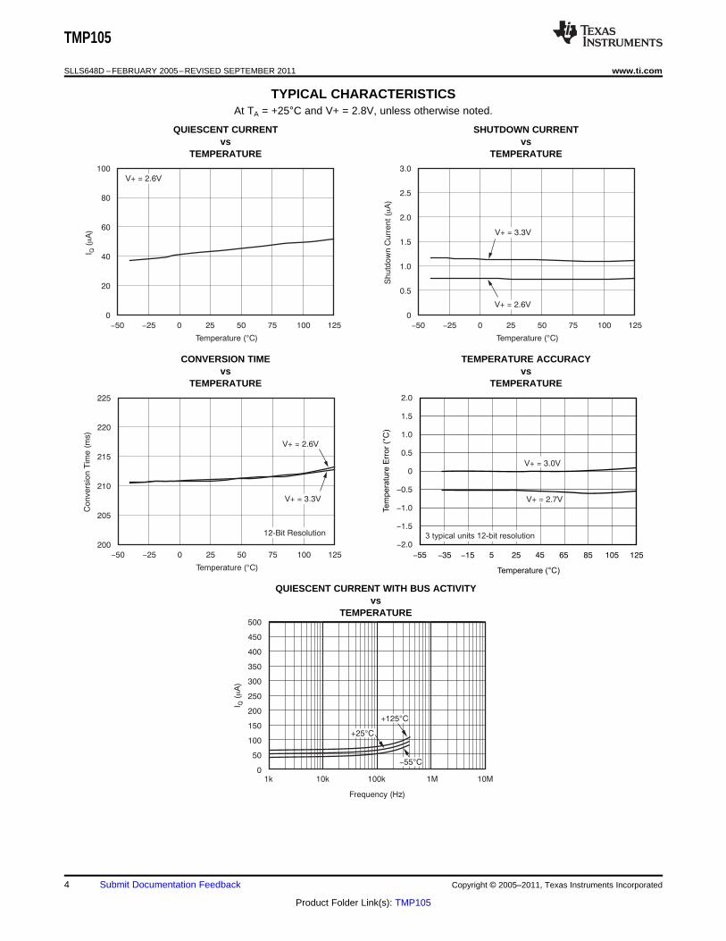
TYPICAL CHARACTERISTICSAt TA = +25°C and V+ = 2.8V, unless otherwise noted.
QUIESCENT CURRENT SHUTDOWN CURRENTvs vs
TEMPERATURE TEMPERATURE
CONVERSION TIME TEMPERATURE ACCURACYvs vs
TEMPERATURE TEMPERATURE
QUIESCENT CURRENT WITH BUS ACTIVITYvs
TEMPERATURE
4 Submit Documentation Feedback Copyright © 2005–2011, Texas Instruments Incorporated
Product Folder Link(s): TMP105
TMP105
0.1 Fm
V+
GND
A2
B2
C1
ALERT
(Output)
C2A0
B1
A1
SCL
SDA
To
Two-Wire
Controller
I/O
Control
Interface
SCL
SDA
Temperature
Register
Configuration
Register
TLOW
Register
THIGH
Register
Pointer
Register
TMP105
www.ti.com SLLS648D –FEBRUARY 2005–REVISED SEPTEMBER 2011
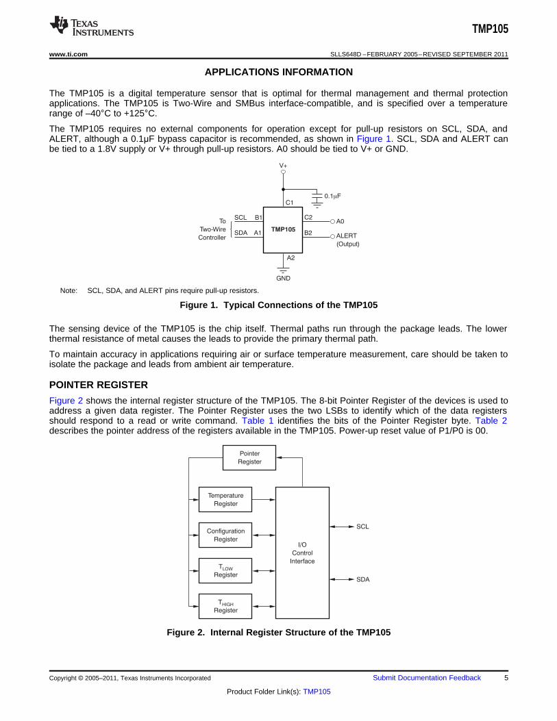
APPLICATIONS INFORMATION
The TMP105 is a digital temperature sensor that is optimal for thermal management and thermal protectionapplications. The TMP105 is Two-Wire and SMBus interface-compatible, and is specified over a temperaturerange of –40°C to +125°C.
The TMP105 requires no external components for operation except for pull-up resistors on SCL, SDA, andALERT, although a 0.1μF bypass capacitor is recommended, as shown in Figure 1. SCL, SDA and ALERT canbe tied to a 1.8V supply or V+ through pull-up resistors. A0 should be tied to V+ or GND.
Note: SCL, SDA, and ALERT pins require pull-up resistors.
Figure 1. Typical Connections of the TMP105
The sensing device of the TMP105 is the chip itself. Thermal paths run through the package leads. The lowerthermal resistance of metal causes the leads to provide the primary thermal path.
To maintain accuracy in applications requiring air or surface temperature measurement, care should be taken toisolate the package and leads from ambient air temperature.
POINTER REGISTER
Figure 2 shows the internal register structure of the TMP105. The 8-bit Pointer Register of the devices is used toaddress a given data register. The Pointer Register uses the two LSBs to identify which of the data registersshould respond to a read or write command. Table 1 identifies the bits of the Pointer Register byte. Table 2describes the pointer address of the registers available in the TMP105. Power-up reset value of P1/P0 is 00.
Figure 2. Internal Register Structure of the TMP105
Copyright © 2005–2011, Texas Instruments Incorporated Submit Documentation Feedback 5
Product Folder Link(s): TMP105

TMP105
SLLS648D –FEBRUARY 2005–REVISED SEPTEMBER 2011 www.ti.com
Table 1. Pointer Register Byte
P7 P6 P5 P4 P3 P2 P1 P0
0 0 0 0 0 0 Register Bits
Table 2. Pointer Addresses of the TMP105
P1 P0 REGISTER
0 0 Temperature Register (Read Only)
0 1 Configuration Register (Read/Write)
1 0 TLOW Register (Read/Write)
1 1 THIGH Register (Read/Write)
TEMPERATURE REGISTER
The Temperature Register of the TMP105 is a 12-bit, read-only register that stores the output of the most recentconversion. Two bytes must be read to obtain data, and are described in Table 3 and Table 4. Note that byte 1 isthe most significant byte; byte 2 is the least significant byte (sent in this order). The first 12 bits are used toindicate temperature, with all remaining bits equal to zero. The least significant byte does not have to be read ifthat information is not needed. Data format for temperature is summarized in Table 5. Following power-up orreset, the Temperature Register will read 0°C until the first conversion is complete.
Table 3. Byte 1 of Temperature Register
D7 D6 D5 D4 D3 D2 D1 D0
T11 T10 T9 T8 T7 T6 T5 T4
Table 4. Byte 2 of Temperature Register
D7 D6 D5 D4 D3 D2 D1 D0
T3 T2 T1 T0 0 0 0 0
Table 5. Temperature Data Format
TEMPERATURE (°C) DIGITAL OUTPUT (BINARY) HEX
128 0111 1111 1111 7FF
127.9375 0111 1111 1111 7FF
100 0110 0100 0000 640
80 0101 0000 0000 500
75 0100 1011 0000 4B0
50 0011 0010 0000 320
25 0001 1001 0000 190
0.25 0000 0000 0100 004
0 0000 0000 0000 000
–0.25 1111 1111 1100 FFC
–25 1110 0111 0000 E70
–55 1100 1001 0000 C90
The user can obtain 9, 10, 11, or 12 bits of resolution by addressing the Configuration Register and setting theresolution bits accordingly. For 9-, 10-, or 11-bit resolution, the most significant bits in the Temperature Registerare used with the unused LSBs set to zero.
6 Submit Documentation Feedback Copyright © 2005–2011, Texas Instruments Incorporated
Product Folder Link(s): TMP105

Measured
Temperature
THIGH
TLOW
TMP105 ALERT PIN
(Comparator Mode)
POL = 0
TMP105 ALERT PIN
(Interrupt Mode)
POL = 0
TMP105 ALERT PIN
(Comparator Mode)
POL = 1
TMP105 ALERT PIN
(Interrupt Mode)
POL = 1
Read Read
Time
Read
TMP105
www.ti.com SLLS648D –FEBRUARY 2005–REVISED SEPTEMBER 2011
CONFIGURATION REGISTER
The Configuration Register is an 8-bit read/write register used to store bits that control the operational modes ofthe temperature sensor. Read/write operations are performed MSB first. The format of the Configuration registerfor the TMP105 is shown in Table 6, followed by a breakdown of the register bits. The power-up/reset value ofthe Configuration Register is all bits equal to 0.
Table 6. Configuration Register Format
BYTE D7 D6 D5 D4 D3 D2 D1 D0
1 OS R1 R0 F1 F0 POL TM SD
SHUTDOWN MODE (SD)
The Shutdown Mode of the TMP105 allows the user to save maximum power by shutting down all devicecircuitry other than the serial interface, which reduces current consumption to typically 1.5μA. Shutdown Mode isenabled when the SD bit is 1; the device will shut down once the current conversion is completed. When SD isequal to 0, the device will maintain a continuous conversion state.
THERMOSTAT MODE (TM)
The Thermostat Mode bit of the TMP105 indicates to the device whether to operate in Comparator Mode (TM =0) or Interrupt Mode (TM = 1). For more information on comparator and interrupt modes, see the High and LowLimit Registers section.
POLARITY (POL)
The Polarity Bit of the TMP105 allows the user to adjust the polarity of the ALERT pin output. If POL = 0, theALERT pin will be active LOW, as shown in Figure 3. For POL = 1, the ALERT pin will be active HIGH, and thestate of the ALERT pin is inverted.
Figure 3. Output Transfer Function Diagrams
Copyright © 2005–2011, Texas Instruments Incorporated Submit Documentation Feedback 7
Product Folder Link(s): TMP105

TMP105
SLLS648D –FEBRUARY 2005–REVISED SEPTEMBER 2011 www.ti.com
FAULT QUEUE (F1/F0)
A fault condition is defined as when the measured temperature exceeds the user-defined limits set in the THIGHand TLOW Registers. Additionally, the number of fault conditions required to generate an alert may beprogrammed using the fault queue. The fault queue is provided to prevent a false alert as a result ofenvironmental noise. The fault queue requires consecutive fault measurements in order to trigger the alertfunction. Table 7 defines the number of measured faults that may be programmed to trigger an alert condition inthe device. For THIGH and TLOW register format and byte order, see the High and Low Limit Registers section.
Table 7. Fault Settings of the TMP105
F1 F0 CONSECUTIVE FAULTS
0 0 1
0 1 2
1 0 4
1 1 6
CONVERTER RESOLUTION (R1/R0)
The Converter Resolution bits control the resolution of the internal analog-to-digital (A/D) converter. This controlallows the user to maximize efficiency by programming for higher resolution or faster conversion time. Table 8identifies the resolution bits and the relationship between resolution and conversion time.
Table 8. Resolution of the TMP105
CONVERSION TIMER1 R0 RESOLUTION (typical)
0 0 9 Bits (0.5°C) 27.5ms
0 1 10 Bits (0.25°C) 55ms
1 0 11 Bits (0.125°C) 110ms
1 1 12 Bits (0.0625°C) 220ms
ONE-SHOT (OS)
The TMP105 features a One-Shot Temperature Measurement Mode. When the device is in Shutdown Mode,writing a ‘1’ to the OS bit starts a single temperature conversion. The device will return to the shutdown state atthe completion of the single conversion. This option is useful to reduce power consumption in the TMP105 whencontinuous temperature monitoring is not required. When the Configuration Register is read, the OS alwaysreads zero.
HIGH AND LOW LIMIT REGISTERS
In Comparator Mode (TM = 0), the ALERT pin of the TMP105 becomes active when the temperature equals orexceeds the value in THIGH and generates a consecutive number of faults according to fault bits F1 and F0. TheALERT pin remains active until the temperature falls below the indicated TLOW value for the same number offaults.
In Interrupt Mode (TM = 1), the ALERT pin becomes active when the temperature equals or exceeds THIGH for aconsecutive number of fault conditions. The ALERT pin remains active until a read operation of any registeroccurs, or until the device successfully responds to the SMBus Alert Response address. The ALERT pin clears ifthe device is placed in Shutdown Mode. Once the ALERT pin is cleared, it will only become active again by thetemperature falling below TLOW. When the temperature falls below TLOW, the ALERT pin becomes active andremains active until cleared by a read operation of any register or a successful response to the SMBus AlertResponse address. When the ALERT pin clears, the above cycle will repeat, with the ALERT pin becomingactive when the temperature equals or exceeds THIGH. The ALERT pin can also be cleared by resetting thedevice with the General Call Reset command. This reset also clears the state of the internal registers in thedevice returning the device to Comparator Mode (TM = 0).
8 Submit Documentation Feedback Copyright © 2005–2011, Texas Instruments Incorporated
Product Folder Link(s): TMP105

TMP105
www.ti.com SLLS648D –FEBRUARY 2005–REVISED SEPTEMBER 2011
Both operational modes are represented in Figure 3. Table 9 and Table 10 describe the format for the THIGH andTLOW Registers. Note that the most significant byte is sent first, followed by the least significant byte. Power-upreset values for THIGH and TLOW are:
THIGH = 80°C and TLOW = 75°C
The format of the data for THIGH and TLOW is the same as for the Temperature Register.
Table 9. Bytes 1 and 2 of THIGH Register
BYTE D7 D6 D5 D4 D3 D2 D1 D0
1 H11 H10 H9 H8 H7 H6 H5 H4
BYTE D7 D6 D5 D4 D3 D2 D1 D0
2 H3 H2 H1 H0 0 0 0 0
Table 10. Bytes 1 and 2 of TLOW Register
BYTE D7 D6 D5 D4 D3 D2 D1 D0
1 L11 L10 L9 L8 L7 L6 L5 L4
BYTE D7 D6 D5 D4 D3 D2 D1 D0
2 L3 L2 L1 L0 0 0 0 0
All 12 bits for the Temperature, THIGH, and TLOW Registers are used in the comparisons for the ALERT functionfor all converter resolutions. The three LSBs in THIGH and TLOW can affect the ALERT output even if the converteris configured for 9-bit resolution.
SERIAL INTERFACE
The TMP105 operates only as a slave device on the Two-Wire bus and SMBus. Connections to the bus aremade via the open-drain I/O lines SDA and SCL. The SDA and SCL pins feature integrated spike suppressionfilters and Schmitt triggers to minimize the effects of input spikes and bus noise. The TMP105 supports thetransmission protocol for fast (1kHz to 400kHz) mode. All data bytes are transmitted MSB first.
SERIAL BUS ADDRESS
To communicate with the TMP105, the master must first address slave devices via a slave address byte. Theslave address byte consists of seven address bits, and a direction bit indicating the intent of executing a read orwrite operation.
The TMP105 features one address pin allowing up to two devices to be connected per bus. Pin logic levels aredescribed in Table 11. The address pin of the TMP105 is read after reset, at start of communication, or inresponse to a Two-Wire address acquire request. Following reading of the state of the pin, the address is latchedto minimize power dissipation associated with detection.
Table 11. Address Pin and Slave Addresses for theTMP105
A0 SLAVE ADDRESS
0 1001000
1 1001001
Copyright © 2005–2011, Texas Instruments Incorporated Submit Documentation Feedback 9
Product Folder Link(s): TMP105

TMP105
SLLS648D –FEBRUARY 2005–REVISED SEPTEMBER 2011 www.ti.com
BUS OVERVIEW
The device that initiates the transfer is called a master, and the devices controlled by the master are slaves. Thebus must be controlled by a master device that generates the serial clock (SCL), controls the bus access, andgenerates the START and STOP conditions.
To address a specific device, a START condition is initiated, indicated by pulling the data-line (SDA) from aHIGH to LOW logic level while SCL is HIGH. All slaves on the bus shift in the slave address byte, with the last bitindicating whether a read or write operation is intended. During the ninth clock pulse, the slave being addressedresponds to the master by generating an Acknowledge and pulling SDA LOW.
Data transfer is then initiated and sent over eight clock pulses followed by an Acknowledge Bit. During datatransfer SDA must remain stable while SCL is HIGH, as any change in SDA while SCL is HIGH will beinterpreted as a control signal.
Once all data has been transferred, the master generates a STOP condition, indicated by pulling SDA from LOWto HIGH while SCL is HIGH.
WRITING/READING TO THE TMP105
Accessing a particular register on the TMP105 is accomplished by writing the appropriate value to the PointerRegister. The value for the Pointer Register is the first byte transferred after the slave address byte with the R/Wbit LOW. Every write operation to the TMP105 requires a value for the Pointer Register. (Refer to Figure 5.)
When reading from the TMP105, the last value stored in the Pointer Register by a write operation is used todetermine which register is read by a read operation. To change the register pointer for a read operation, a newvalue must be written to the Pointer Register. This is accomplished by issuing a slave address byte with the R/Wbit LOW, followed by the Pointer Register byte. No additional data are required. The master can then generate aSTART condition and send the slave address byte with the R/W bit HIGH to initiate the read command. SeeFigure 6 for details of this sequence. If repeated reads from the same register are desired, it is not necessary tocontinually send the Pointer Register byte, as the TMP105 remembers the Pointer Register value until it ischanged by the next write operation.
Note that register bytes are sent most significant byte first, followed by the least significant byte.
SLAVE MODE OPERATIONS
The TMP105 can operate as a slave receiver or slave transmitter.
Slave Receiver Mode:
The first byte transmitted by the master is the slave address, with the R/W bit LOW. The TMP105 thenacknowledges reception of a valid address. The next byte transmitted by the master is the Pointer Register. TheTMP105 then acknowledges reception of the Pointer Register byte. The next byte or bytes are written to theregister addressed by the Pointer Register. The TMP105 acknowledges reception of each data byte. The mastermay terminate data transfer by generating a START or STOP condition.
Slave Transmitter Mode:
The first byte is transmitted by the master and is the slave address, with the R/W bit HIGH. The slaveacknowledges reception of a valid slave address. The next byte is transmitted by the slave and is the mostsignificant byte of the register indicated by the Pointer Register. The master acknowledges reception of the databyte. The next byte transmitted by the slave is the least significant byte. The master acknowledges reception ofthe data byte. The master may terminate data transfer by generating a Not-Acknowledge on reception of anydata byte, or generating a START or STOP condition.
10 Submit Documentation Feedback Copyright © 2005–2011, Texas Instruments Incorporated
Product Folder Link(s): TMP105

TMP105
www.ti.com SLLS648D –FEBRUARY 2005–REVISED SEPTEMBER 2011
SMBus ALERT FUNCTION
The TMP105 supports the SMBus Alert function. When the TMP105 is operating in Interrupt Mode (TM = 1), theALERT pin of the TMP105 may be connected as an SMBus Alert signal. When a master senses that an ALERTcondition is present on the ALERT line, the master sends an SMBus Alert command (00011001) on the bus. Ifthe ALERT pin of the TMP105 is active, the devices will acknowledge the SMBus Alert command and respond byreturning its slave address on the SDA line. The eighth bit (LSB) of the slave address byte will indicate if thetemperature exceeding THIGH or falling below TLOW caused the ALERT condition. This bit will be HIGH if thetemperature is greater than or equal to THIGH. This bit will be LOW if the temperature is less than TLOW. Refer toFigure 7 for details of this sequence.
If multiple devices on the bus respond to the SMBus Alert command, arbitration during the slave address portionof the SMBus Alert command will determine which device will clear its ALERT status. If the TMP105 wins thearbitration, its ALERT pin will become inactive at the completion of the SMBus Alert command. If the TMP105loses the arbitration, its ALERT pin will remain active.
GENERAL CALL
The TMP105 responds to a Two-Wire General Call address (0000000) if the eighth bit is 0. The device willacknowledge the General Call address and respond to commands in the second byte. If the second byte is00000100, the TMP105 will latch the status of the address pin, but will not reset. If the second byte is 00000110,the TMP105 will latch the status of the address pin and reset the internal registers to their power-up values.
TIMEOUT FUNCTION
The TMP105 will reset the serial interface if either SCL or SDA are held LOW for 54ms (typ) between a STARTand STOP condition. The TMP105 will release the bus if it is pulled LOW and will wait for a START condition. Toavoid activating the timeout function, it is necessary to maintain a communication speed of at least 1kHz for SCLoperating frequency.
TIMING DIAGRAMS
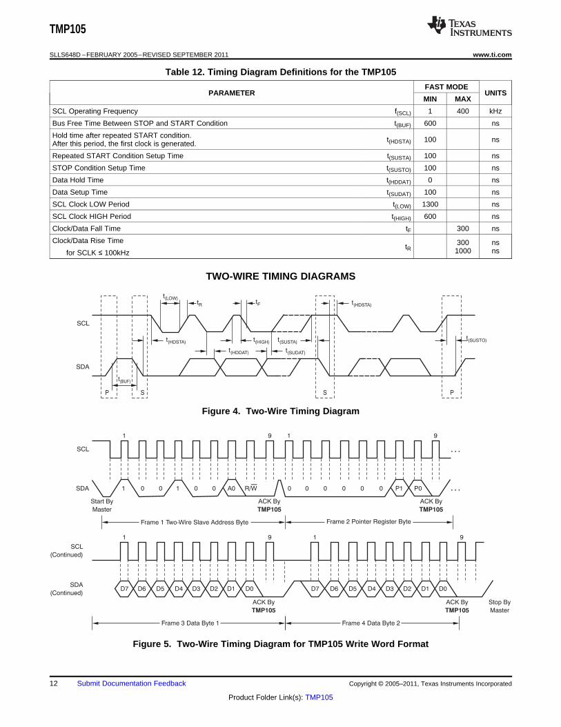
The TMP105 is Two-Wire and SMBus-compatible. Figure 4 to Figure 7 describe the various operations on theTMP105. Bus definitions are given below. Parameters for Figure 4 are defined in Table 12.
Bus Idle:
Both SDA and SCL lines remain HIGH.
Start Data Transfer:
A change in the state of the SDA line, from HIGH to LOW, while the SCL line is HIGH, defines a STARTcondition. Each data transfer is initiated with a START condition.
Stop Data Transfer:
A change in the state of the SDA line from LOW to HIGH while the SCL line is HIGH defines a STOP condition.Each data transfer is terminated with a repeated START or STOP condition.
Data Transfer:
The number of data bytes transferred between a START and a STOP condition is not limited and is determinedby the master device. The receiver acknowledges the transfer of data.
Acknowledge:
Each receiving device, when addressed, is obliged to generate an Acknowledge bit. A device that acknowledgesmust pull down the SDA line during the Acknowledge clock pulse in such a way that the SDA line is stable LOWduring the HIGH period of the Acknowledge clock pulse. Setup and hold times must be taken into account. On amaster receive, the termination of the data transfer can be signaled by the master generating a Not-Acknowledgeon the last byte that has been transmitted by the slave.
Copyright © 2005–2011, Texas Instruments Incorporated Submit Documentation Feedback 11
Product Folder Link(s): TMP105
SCL
SDA
t(LOW)tR tF t(HDSTA)
t(HDSTA)
t(HDDAT)
t(BUF)
t(SUDAT)
t(HIGH) t(SUSTA)t(SUSTO)
P S S P
Frame 1 Two-Wire Slave Address Byte Frame 2 Pointer Register Byte
Frame 4 Data Byte 2
1
Start By
Master
ACK By
TMP105
ACK By
TMP105
ACK By
TMP105
Stop By
Master
1 9 1
1
D7 D6 D5 D4 D3 D2 D1 D0
9
Frame 3 Data Byte 1
ACK By
TMP105
1
D7SDA
(Continued)
SCL
(Continued)
D6 D5 D4 D3 D2 D1 D0
9
9
SDA
SCL
0 0 1 0 0 A0 R/W 0 0 0 0 0 0 P1 P0 ¼
¼
TMP105
SLLS648D –FEBRUARY 2005–REVISED SEPTEMBER 2011 www.ti.com
Table 12. Timing Diagram Definitions for the TMP105
FAST MODEPARAMETER UNITS
MIN MAX
SCL Operating Frequency f(SCL) 1 400 kHz
Bus Free Time Between STOP and START Condition t(BUF) 600 ns
Hold time after repeated START condition. t(HDSTA) 100 nsAfter this period, the first clock is generated.
Repeated START Condition Setup Time t(SUSTA) 100 ns
STOP Condition Setup Time t(SUSTO) 100 ns
Data Hold Time t(HDDAT) 0 ns
Data Setup Time t(SUDAT) 100 ns
SCL Clock LOW Period t(LOW) 1300 ns
SCL Clock HIGH Period t(HIGH) 600 ns
Clock/Data Fall Time tF 300 ns
Clock/Data Rise Time 300 nstR 1000 nsfor SCLK ≤ 100kHz
TWO-WIRE TIMING DIAGRAMS
Figure 4. Two-Wire Timing Diagram
Figure 5. Two-Wire Timing Diagram for TMP105 Write Word Format
12 Submit Documentation Feedback Copyright © 2005–2011, Texas Instruments Incorporated
Product Folder Link(s): TMP105

Frame 1 Two-Wire Slave Address Byte Frame 2 Pointer Register Byte
1
Start By
Master
ACK By
TMP105
ACK By
TMP105
Frame 3 Two-Wire Slave Address Byte Frame 4 Data Byte 1 Read Register
Start By
Master
ACK By
TMP105
ACK By
Master
From
TMP105
1 9 1 9
1 9 1 9
SDA
SCL
0 0 R/W 0 0 0 0 0 0 P1 P0 ¼
¼
¼
¼
SDA
(Continued)
SCL
(Continued)
SDA
(Continued)
SCL
(Continued)
1 0 0 1
0 0 A0
0 0 A0 R/W D7 D6 D5 D4 D3 D2 D1 D0
Frame 5 Data Byte 2 Read Register
Stop By
Master
ACK By
Master
From
TMP105
1 9
D7 D6 D5 D4 D3 D2 D1 D0
Frame 1 SMBus ALERT Response Address Byte Frame 2 Slave Address Byte
Start By
Master
ACK By
TMP105
From
TMP105
NACK By
Master
Stop By
Master
1 9 1 9
SDA
SCL
ALERT
0 0 0 1 1 0 0 R/W 1 0 0 1 0 0 A0 Status
TMP105
www.ti.com SLLS648D –FEBRUARY 2005–REVISED SEPTEMBER 2011
Figure 6. Two-Wire Timing Diagram for Read Word Format
Figure 7. Timing Diagram for SMBus ALERT
Copyright © 2005–2011, Texas Instruments Incorporated Submit Documentation Feedback 13
Product Folder Link(s): TMP105

TMP105
SLLS648D –FEBRUARY 2005–REVISED SEPTEMBER 2011 www.ti.com
REVISION HISTORY
NOTE: Page numbers for previous revisions may differ from page numbers in the current version.
Changes from Revision C (April, 2008) to Revision D Page
• Updated document format to current standards ................................................................................................................... 1
• Added Absolute Maximum Ratings table .............................................................................................................................. 2
• In the Electrical Specifications table, changed from: DIGITAL INPUT/OUTPUT to: DIGITAL INPUT/OUTPUT (SCL,SDA, ALERT) ........................................................................................................................................................................ 3
• In the Electrical Specifications table, added the DIGITAL INPUT (A0) section .................................................................... 3
• Changed max spec for VIH logic level ................................................................................................................................... 3
• Changed test conditions for leakage input current ............................................................................................................... 3
• Updated Temperature Accuracy vs Temperature typical characteristic graph ..................................................................... 4
• Added text to the Application Information section, first paragraph ....................................................................................... 5
• Corrected typos in Figure 1 .................................................................................................................................................. 5
Changes from Revision B (January, 2006) to Revision C Page
• Added labels to Temperature Accuracy vs Temperature typical characteristic graph ......................................................... 4
14 Submit Documentation Feedback Copyright © 2005–2011, Texas Instruments Incorporated
Product Folder Link(s): TMP105
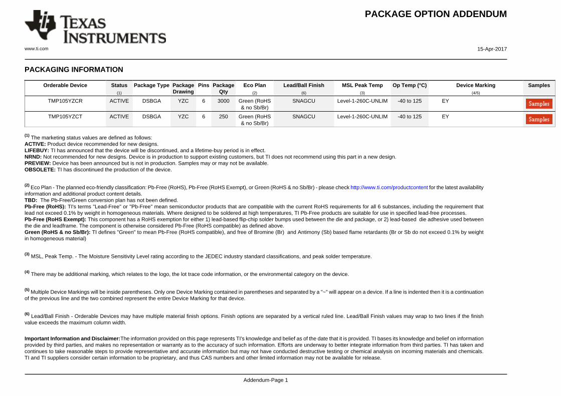
PACKAGE OPTION ADDENDUM
www.ti.com 15-Apr-2017
Addendum-Page 1
PACKAGING INFORMATION
Orderable Device Status(1)
Package Type PackageDrawing
Pins PackageQty
Eco Plan(2)
Lead/Ball Finish(6)
MSL Peak Temp(3)
Op Temp (°C) Device Marking(4/5)
Samples
TMP105YZCR ACTIVE DSBGA YZC 6 3000 Green (RoHS& no Sb/Br)
SNAGCU Level-1-260C-UNLIM -40 to 125 EY
TMP105YZCT ACTIVE DSBGA YZC 6 250 Green (RoHS& no Sb/Br)
SNAGCU Level-1-260C-UNLIM -40 to 125 EY
(1) The marketing status values are defined as follows:ACTIVE: Product device recommended for new designs.LIFEBUY: TI has announced that the device will be discontinued, and a lifetime-buy period is in effect.NRND: Not recommended for new designs. Device is in production to support existing customers, but TI does not recommend using this part in a new design.PREVIEW: Device has been announced but is not in production. Samples may or may not be available.OBSOLETE: TI has discontinued the production of the device.
(2) Eco Plan - The planned eco-friendly classification: Pb-Free (RoHS), Pb-Free (RoHS Exempt), or Green (RoHS & no Sb/Br) - please check http://www.ti.com/productcontent for the latest availabilityinformation and additional product content details.TBD: The Pb-Free/Green conversion plan has not been defined.Pb-Free (RoHS): TI's terms "Lead-Free" or "Pb-Free" mean semiconductor products that are compatible with the current RoHS requirements for all 6 substances, including the requirement thatlead not exceed 0.1% by weight in homogeneous materials. Where designed to be soldered at high temperatures, TI Pb-Free products are suitable for use in specified lead-free processes.Pb-Free (RoHS Exempt): This component has a RoHS exemption for either 1) lead-based flip-chip solder bumps used between the die and package, or 2) lead-based die adhesive used betweenthe die and leadframe. The component is otherwise considered Pb-Free (RoHS compatible) as defined above.Green (RoHS & no Sb/Br): TI defines "Green" to mean Pb-Free (RoHS compatible), and free of Bromine (Br) and Antimony (Sb) based flame retardants (Br or Sb do not exceed 0.1% by weightin homogeneous material)
(3) MSL, Peak Temp. - The Moisture Sensitivity Level rating according to the JEDEC industry standard classifications, and peak solder temperature.
(4) There may be additional marking, which relates to the logo, the lot trace code information, or the environmental category on the device.
(5) Multiple Device Markings will be inside parentheses. Only one Device Marking contained in parentheses and separated by a "~" will appear on a device. If a line is indented then it is a continuationof the previous line and the two combined represent the entire Device Marking for that device.
(6) Lead/Ball Finish - Orderable Devices may have multiple material finish options. Finish options are separated by a vertical ruled line. Lead/Ball Finish values may wrap to two lines if the finishvalue exceeds the maximum column width.
Important Information and Disclaimer:The information provided on this page represents TI's knowledge and belief as of the date that it is provided. TI bases its knowledge and belief on informationprovided by third parties, and makes no representation or warranty as to the accuracy of such information. Efforts are underway to better integrate information from third parties. TI has taken andcontinues to take reasonable steps to provide representative and accurate information but may not have conducted destructive testing or chemical analysis on incoming materials and chemicals.TI and TI suppliers consider certain information to be proprietary, and thus CAS numbers and other limited information may not be available for release.

PACKAGE OPTION ADDENDUM
www.ti.com 15-Apr-2017
Addendum-Page 2
In no event shall TI's liability arising out of such information exceed the total purchase price of the TI part(s) at issue in this document sold by TI to Customer on an annual basis.

TAPE AND REEL INFORMATION
*All dimensions are nominal
Device PackageType
PackageDrawing
Pins SPQ ReelDiameter
(mm)
ReelWidth
W1 (mm)
A0(mm)
B0(mm)
K0(mm)
P1(mm)
W(mm)
Pin1Quadrant
TMP105YZCR DSBGA YZC 6 3000 178.0 8.4 1.24 1.7 0.76 4.0 8.0 Q1
TMP105YZCT DSBGA YZC 6 250 178.0 8.4 1.24 1.7 0.76 4.0 8.0 Q1
PACKAGE MATERIALS INFORMATION
www.ti.com 18-Aug-2014
Pack Materials-Page 1

*All dimensions are nominal
Device Package Type Package Drawing Pins SPQ Length (mm) Width (mm) Height (mm)
TMP105YZCR DSBGA YZC 6 3000 220.0 220.0 35.0
TMP105YZCT DSBGA YZC 6 250 220.0 220.0 35.0
PACKAGE MATERIALS INFORMATION
www.ti.com 18-Aug-2014
Pack Materials-Page 2

www.ti.com
PACKAGE OUTLINE
C0.625 MAX
0.350.15
1TYP
0.25 TYP
6X 0.350.25
0.5TYP
0.5 TYP
B E A
D
4219522/A 02/2015
DSBGA - 0.625 mm max heightYZC0006DIE SIZE BALL GRID ARRAY
NOTES: 1. All linear dimensions are in millimeters. Any dimensions in parenthesis are for reference only. Dimensioning and tolerancing per ASME Y14.5M.2. This drawing is subject to change without notice.3. NanoFreeTM package configuration.
NanoFree Is a trademark of Texas Instruments.
BALL A1CORNER
SEATING PLANE
BALL TYP 0.08 C
A
1
0.015 C A B
SYMM
SYMM
C
2
B
SCALE 9.000
D: Max =
E: Max =
1.61 mm, Min =
1.11 mm, Min =
1.55 mm
1.05 mm
www.ti.com
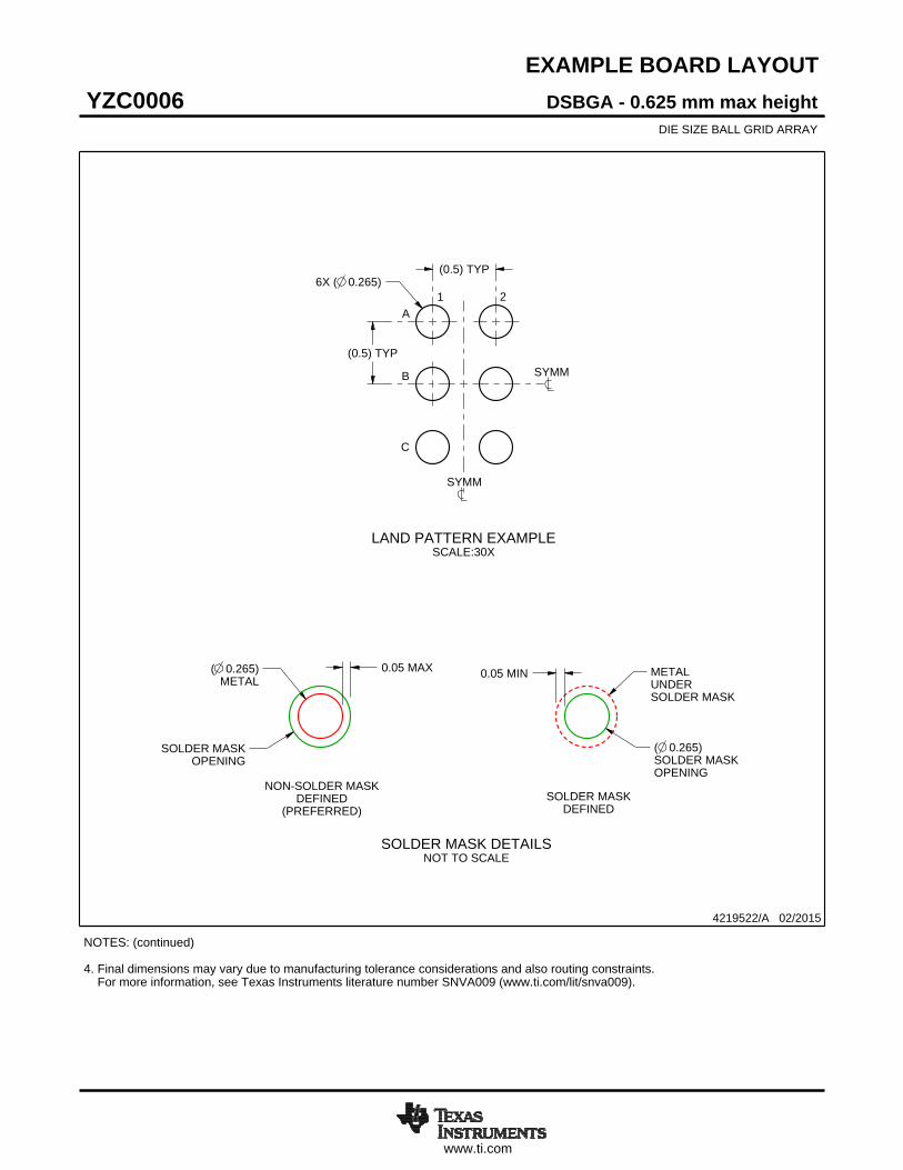
EXAMPLE BOARD LAYOUT
6X ( )0.265(0.5) TYP
(0.5) TYP
( )METAL0.265 0.05 MAX
SOLDER MASKOPENING
METALUNDERSOLDER MASK
( )SOLDER MASKOPENING
0.265
0.05 MIN
4219522/A 02/2015
DSBGA - 0.625 mm max heightYZC0006DIE SIZE BALL GRID ARRAY
NOTES: (continued) 4. Final dimensions may vary due to manufacturing tolerance considerations and also routing constraints. For more information, see Texas Instruments literature number SNVA009 (www.ti.com/lit/snva009).
SYMM
SYMM
LAND PATTERN EXAMPLESCALE:30X
1 2A
B
C
NON-SOLDER MASKDEFINED
(PREFERRED)
SOLDER MASK DETAILSNOT TO SCALE
SOLDER MASKDEFINED

www.ti.com
EXAMPLE STENCIL DESIGN
(0.5)TYP
(0.5) TYP
6X ( 0.25)(R ) TYP0.05
METALTYP
4219522/A 02/2015
DSBGA - 0.625 mm max heightYZC0006DIE SIZE BALL GRID ARRAY
NOTES: (continued) 5. Laser cutting apertures with trapezoidal walls and rounded corners may offer better paste release.
SYMM
SYMM
SOLDER PASTE EXAMPLEBASED ON 0.1 mm THICK STENCIL
SCALE:40X
1 2
A
B
C

IMPORTANT NOTICE
Texas Instruments Incorporated (TI) reserves the right to make corrections, enhancements, improvements and other changes to itssemiconductor products and services per JESD46, latest issue, and to discontinue any product or service per JESD48, latest issue. Buyersshould obtain the latest relevant information before placing orders and should verify that such information is current and complete.TI’s published terms of sale for semiconductor products (http://www.ti.com/sc/docs/stdterms.htm) apply to the sale of packaged integratedcircuit products that TI has qualified and released to market. Additional terms may apply to the use or sale of other types of TI products andservices.Reproduction of significant portions of TI information in TI data sheets is permissible only if reproduction is without alteration and isaccompanied by all associated warranties, conditions, limitations, and notices. TI is not responsible or liable for such reproduceddocumentation. Information of third parties may be subject to additional restrictions. Resale of TI products or services with statementsdifferent from or beyond the parameters stated by TI for that product or service voids all express and any implied warranties for theassociated TI product or service and is an unfair and deceptive business practice. TI is not responsible or liable for any such statements.Buyers and others who are developing systems that incorporate TI products (collectively, “Designers”) understand and agree that Designersremain responsible for using their independent analysis, evaluation and judgment in designing their applications and that Designers havefull and exclusive responsibility to assure the safety of Designers' applications and compliance of their applications (and of all TI productsused in or for Designers’ applications) with all applicable regulations, laws and other applicable requirements. Designer represents that, withrespect to their applications, Designer has all the necessary expertise to create and implement safeguards that (1) anticipate dangerousconsequences of failures, (2) monitor failures and their consequences, and (3) lessen the likelihood of failures that might cause harm andtake appropriate actions. Designer agrees that prior to using or distributing any applications that include TI products, Designer willthoroughly test such applications and the functionality of such TI products as used in such applications.TI’s provision of technical, application or other design advice, quality characterization, reliability data or other services or information,including, but not limited to, reference designs and materials relating to evaluation modules, (collectively, “TI Resources”) are intended toassist designers who are developing applications that incorporate TI products; by downloading, accessing or using TI Resources in anyway, Designer (individually or, if Designer is acting on behalf of a company, Designer’s company) agrees to use any particular TI Resourcesolely for this purpose and subject to the terms of this Notice.TI’s provision of TI Resources does not expand or otherwise alter TI’s applicable published warranties or warranty disclaimers for TIproducts, and no additional obligations or liabilities arise from TI providing such TI Resources. TI reserves the right to make corrections,enhancements, improvements and other changes to its TI Resources. TI has not conducted any testing other than that specificallydescribed in the published documentation for a particular TI Resource.Designer is authorized to use, copy and modify any individual TI Resource only in connection with the development of applications thatinclude the TI product(s) identified in such TI Resource. NO OTHER LICENSE, EXPRESS OR IMPLIED, BY ESTOPPEL OR OTHERWISETO ANY OTHER TI INTELLECTUAL PROPERTY RIGHT, AND NO LICENSE TO ANY TECHNOLOGY OR INTELLECTUAL PROPERTYRIGHT OF TI OR ANY THIRD PARTY IS GRANTED HEREIN, including but not limited to any patent right, copyright, mask work right, orother intellectual property right relating to any combination, machine, or process in which TI products or services are used. Informationregarding or referencing third-party products or services does not constitute a license to use such products or services, or a warranty orendorsement thereof. Use of TI Resources may require a license from a third party under the patents or other intellectual property of thethird party, or a license from TI under the patents or other intellectual property of TI.TI RESOURCES ARE PROVIDED “AS IS” AND WITH ALL FAULTS. TI DISCLAIMS ALL OTHER WARRANTIES ORREPRESENTATIONS, EXPRESS OR IMPLIED, REGARDING RESOURCES OR USE THEREOF, INCLUDING BUT NOT LIMITED TOACCURACY OR COMPLETENESS, TITLE, ANY EPIDEMIC FAILURE WARRANTY AND ANY IMPLIED WARRANTIES OFMERCHANTABILITY, FITNESS FOR A PARTICULAR PURPOSE, AND NON-INFRINGEMENT OF ANY THIRD PARTY INTELLECTUALPROPERTY RIGHTS. TI SHALL NOT BE LIABLE FOR AND SHALL NOT DEFEND OR INDEMNIFY DESIGNER AGAINST ANY CLAIM,INCLUDING BUT NOT LIMITED TO ANY INFRINGEMENT CLAIM THAT RELATES TO OR IS BASED ON ANY COMBINATION OFPRODUCTS EVEN IF DESCRIBED IN TI RESOURCES OR OTHERWISE. IN NO EVENT SHALL TI BE LIABLE FOR ANY ACTUAL,DIRECT, SPECIAL, COLLATERAL, INDIRECT, PUNITIVE, INCIDENTAL, CONSEQUENTIAL OR EXEMPLARY DAMAGES INCONNECTION WITH OR ARISING OUT OF TI RESOURCES OR USE THEREOF, AND REGARDLESS OF WHETHER TI HAS BEENADVISED OF THE POSSIBILITY OF SUCH DAMAGES.Unless TI has explicitly designated an individual product as meeting the requirements of a particular industry standard (e.g., ISO/TS 16949and ISO 26262), TI is not responsible for any failure to meet such industry standard requirements.Where TI specifically promotes products as facilitating functional safety or as compliant with industry functional safety standards, suchproducts are intended to help enable customers to design and create their own applications that meet applicable functional safety standardsand requirements. Using products in an application does not by itself establish any safety features in the application. Designers mustensure compliance with safety-related requirements and standards applicable to their applications. Designer may not use any TI products inlife-critical medical equipment unless authorized officers of the parties have executed a special contract specifically governing such use.Life-critical medical equipment is medical equipment where failure of such equipment would cause serious bodily injury or death (e.g., lifesupport, pacemakers, defibrillators, heart pumps, neurostimulators, and implantables). Such equipment includes, without limitation, allmedical devices identified by the U.S. Food and Drug Administration as Class III devices and equivalent classifications outside the U.S.TI may expressly designate certain products as completing a particular qualification (e.g., Q100, Military Grade, or Enhanced Product).Designers agree that it has the necessary expertise to select the product with the appropriate qualification designation for their applicationsand that proper product selection is at Designers’ own risk. Designers are solely responsible for compliance with all legal and regulatoryrequirements in connection with such selection.Designer will fully indemnify TI and its representatives against any damages, costs, losses, and/or liabilities arising out of Designer’s non-compliance with the terms and provisions of this Notice.
Mailing Address: Texas Instruments, Post Office Box 655303, Dallas, Texas 75265Copyright © 2017, Texas Instruments Incorporated


![AK9754AE English Datasheet · [AK9754] 018006915-E-00 2018/06-4-5.Pin Configurations and Functions 5.1.Pin Configurations 4 1 2 3 8 7 6 5 VSS VDD CAD0 CAD1 SCL SDA INTN SYNC SCL SDA](https://static.fdocuments.us/doc/165x107/601ad8b72a6c616e353f1c33/ak9754ae-english-datasheet-ak9754-018006915-e-00-201806-4-5pin-configurations.jpg)