
TLV3012-Q1 Low Power Comparator With Integrated Voltage ...
24
Units Reference Voltage – V 500 450 400 350 300 250 200 150 100 50 0 1.230 1.232 1.234 1.236 1.238 1.240 1.242 1.244 1.246 1.248 1.250 1.252 1.254 Reference Voltage – V Temperature – °C 1.250 1.245 1.240 1.235 1.230 1.225 1.220 1.215 1.210 -100 50 100 -50 0 150 Product Folder Order Now Technical Documents Tools & Software Support & Community An IMPORTANT NOTICE at the end of this data sheet addresses availability, warranty, changes, use in safety-critical applications, intellectual property matters and other important disclaimers. PRODUCTION DATA. TLV3012-Q1 SBOS551A – MARCH 2011 – REVISED JUNE 2019 TLV3012-Q1 Low Power Comparator With Integrated Voltage Reference 1 1 Features 1• Qualified for automotive applications • AEC-Q100 qualified with the following results: – Device temperature grade 1: –40°C to +125°C ambient operating temperature range – Device HBM ESD classification level 2 – Device CDM ESD classification level C6 • Low quiescent current = 5 μA (Max) • Integrated voltage reference = 1.242 V • Input common-mode range = 200 mV beyond rails • Voltage reference initial accuracy = 1% • Push-pull output • Low supply voltage = 1.8 V to 5.5 V 2 Applications • Lane departure warning • Cluster • Toll tag • Asset tracking • Battery management systems 3 Description The TLV3012-Q1 device is a push-pull output comparator. The device features an uncommitted on- chip voltage reference and has a 5-μA (max) quiescent current, an input common-mode range 200 mV beyond the supply rails, and single-supply operation from 1.8 V to 5.5 V. The integrated 1.242-V series voltage reference offers low 100-ppm/°C (maximum) drift, is stable with up to 10-nF capacitive load, and can provide up to 0.5 mA (typical) of output current. The TLV3012-Q1 device is available in the SOT (DCK) package. The device is specified for the temperature range of –40°C to +125°C. Device Information (1) PART NUMBER PACKAGE BODY SIZE (NOM) TLV3012-Q1 SOT (6) 2.00 mm × 1.25 mm (1) For all available packages, see the orderable addendum at the end of the data sheet. Reference Voltage Distribution Reference Voltage vs Temperature
Transcript of TLV3012-Q1 Low Power Comparator With Integrated Voltage ...

Uni
ts
Reference Voltage – V
500
450
400
350
300
250
200
150
100
50
0
1.23
0
1.23
2
1.23
4
1.23
6
1.23
8
1.24
0
1.24
2
1.24
4
1.24
6
1.24
8
1.25
0
1.25
2
1.25
4
Ref
eren
ceVo
ltage
–V
Temperature – °C
1.250
1.245
1.240
1.235
1.230
1.225
1.220
1.215
1.210-100 50 100-50 0 150
Product
Folder
Order
Now
Technical
Documents
Tools &
Software
Support &Community
An IMPORTANT NOTICE at the end of this data sheet addresses availability, warranty, changes, use in safety-critical applications,intellectual property matters and other important disclaimers. PRODUCTION DATA.
TLV3012-Q1SBOS551A –MARCH 2011–REVISED JUNE 2019
TLV3012-Q1 Low Power Comparator With Integrated Voltage Reference
1
1 Features1• Qualified for automotive applications• AEC-Q100 qualified with the following results:
– Device temperature grade 1: –40°C to +125°Cambient operating temperature range
– Device HBM ESD classification level 2– Device CDM ESD classification level C6
• Low quiescent current = 5 μA (Max)• Integrated voltage reference = 1.242 V• Input common-mode range = 200 mV beyond rails• Voltage reference initial accuracy = 1%• Push-pull output• Low supply voltage = 1.8 V to 5.5 V
2 Applications• Lane departure warning• Cluster• Toll tag• Asset tracking• Battery management systems
3 DescriptionThe TLV3012-Q1 device is a push-pull outputcomparator. The device features an uncommitted on-chip voltage reference and has a 5-μA (max)quiescent current, an input common-mode range200 mV beyond the supply rails, and single-supplyoperation from 1.8 V to 5.5 V. The integrated 1.242-Vseries voltage reference offers low 100-ppm/°C(maximum) drift, is stable with up to 10-nF capacitiveload, and can provide up to 0.5 mA (typical) of outputcurrent.
The TLV3012-Q1 device is available in the SOT(DCK) package. The device is specified for thetemperature range of –40°C to +125°C.
Device Information(1)
PART NUMBER PACKAGE BODY SIZE (NOM)TLV3012-Q1 SOT (6) 2.00 mm × 1.25 mm
(1) For all available packages, see the orderable addendum atthe end of the data sheet.
Reference Voltage Distribution Reference Voltage vs Temperature

2
TLV3012-Q1SBOS551A –MARCH 2011–REVISED JUNE 2019 www.ti.com
Product Folder Links: TLV3012-Q1
Submit Documentation Feedback Copyright © 2011–2019, Texas Instruments Incorporated
Table of Contents1 Features .................................................................. 12 Applications ........................................................... 13 Description ............................................................. 14 Revision History..................................................... 25 Pin Configuration and Functions ......................... 36 Specifications......................................................... 4
6.1 Absolute Maximum Ratings ...................................... 46.2 ESD Ratings.............................................................. 46.3 Recommended Operating Conditions....................... 46.4 Thermal Information .................................................. 46.5 Electrical Characteristics........................................... 56.6 Switching Characteristics .......................................... 5
7 Typical Characteristics.......................................... 68 Detailed Description ............................................ 10
8.1 Overview ................................................................. 108.2 Functional Block Diagram ....................................... 108.3 Feature Description................................................. 10
8.4 Device Functional Modes........................................ 109 Application and Implementation ........................ 11
9.1 Application Information............................................ 119.2 Typical Application .................................................. 129.3 System Examples ................................................... 14
10 Power Supply Recommendations ..................... 1611 Layout................................................................... 16
11.1 Layout Guidelines ................................................. 1611.2 Layout Example .................................................... 16
12 Device and Documentation Support ................. 1712.1 Receiving Notification of Documentation Updates 1712.2 Community Resources.......................................... 1712.3 Trademarks ........................................................... 1712.4 Electrostatic Discharge Caution............................ 1712.5 Glossary ................................................................ 17
13 Mechanical, Packaging, and OrderableInformation ........................................................... 17
4 Revision HistoryNOTE: Page numbers for previous revisions may differ from page numbers in the current version.
Changes from Original (March 2011) to Revision A Page
• Added the HBM and CDM ESD ratings and classification levels. Also added the AEC-Q100 device temperaturegrade ...................................................................................................................................................................................... 1
• Changed the Applications list ................................................................................................................................................. 1• Added Pin Configuration and Functions section, ESD Ratings table, Feature Description section, Device Functional
Modes, Application and Implementation section, Power Supply Recommendations section, Layout section, Deviceand Documentation Support section, and Mechanical, Packaging, and Orderable Information section ............................... 1
• Deleted the TLV3011-Q1 device from the data sheet and removed A from the TLV3012-Q1 part number ......................... 1• Deleted the Package Ordering Information section................................................................................................................ 3• Moved the switching characteristics from the Electrical Characteristics table to the Switching Characteristics table........... 5

1
2
3
6
5
4
V+
REF
IN-
OUT
V
IN+
3
TLV3012-Q1www.ti.com SBOS551A –MARCH 2011–REVISED JUNE 2019
Product Folder Links: TLV3012-Q1
Submit Documentation FeedbackCopyright © 2011–2019, Texas Instruments Incorporated
5 Pin Configuration and Functions
DCK Package6-Pin SOTTop View
Pin FunctionsPIN
I/O/P DESCRIPTIONNO. NAME1 OUT O Comparator output2 V– P Negative (lowest) power supply3 IN+ I Non-inverting comparator input4 IN– I Inverting comparator input5 REF P Reference output6 V+ P Positive (highest) power supply

4
TLV3012-Q1SBOS551A –MARCH 2011–REVISED JUNE 2019 www.ti.com
Product Folder Links: TLV3012-Q1
Submit Documentation Feedback Copyright © 2011–2019, Texas Instruments Incorporated
(1) Stresses beyond those listed under Absolute Maximum Ratings may cause permanent damage to the device. These are stress ratingsonly, which do not imply functional operation of the device at these or any other conditions beyond those indicated under RecommendedOperating Conditions. Exposure to absolute-maximum-rated conditions for extended periods may affect device reliability.
(2) All voltage values are with respect to the network ground pin.(3) Short circuit to ground
6 Specifications
6.1 Absolute Maximum RatingsOver operating free-air temperature range (unless otherwise noted) (1).
MIN MAX UNITSupply voltage 7 V
Signal input pinsVoltage (2) –0.5 (V+) +0.5 VCurrent (2) ±10 mA
Output short circuit (3) ContinuosOperating temperature –40 125 °C
TJ Junction temperature 150 °CTstg Storage temperature –65 150 °C
(1) AEC Q100-002 indicates that HBM stressing shall be in accordance with the ANSI/ESDA/JEDEC JS-001 specification.
6.2 ESD RatingsVALUE UNIT
V(ESD) Electrostatic dischargeHuman-body model (HBM), per AEC Q100-002 (1) ±2000
VCharged-device model (CDM), per AEC Q100-011 ±1000
6.3 Recommended Operating Conditionsover operating free-air temperature range (unless otherwise noted)
MIN MAX UNITSupply Voltage (V+) – (V–) 1.8 5.5 VAmbientTemperature TA –40 125 °C
(1) For more information about traditional and new thermal metrics, see the Semiconductor and IC Package Thermal Metrics applicationreport.
6.4 Thermal Information
THERMAL METRIC (1)TLV3012-Q1
UNITDCK (SOT)6 PINS
RθJA Junction-to-ambient thermal resistance 168.5 °C/WRθJC(top) Junction-to-case (top) thermal resistance 66.3 °C/WRθJB Junction-to-board thermal resistance 68.9 °C/WψJT Junction-to-top characterization parameter 1.6 °C/WψJB Junction-to-board characterization parameter 67.6 °C/WRθJC(bot) Junction-to-case (bottom) thermal resistance — °C/W

5
TLV3012-Q1www.ti.com SBOS551A –MARCH 2011–REVISED JUNE 2019
Product Folder Links: TLV3012-Q1
Submit Documentation FeedbackCopyright © 2011–2019, Texas Instruments Incorporated
6.5 Electrical CharacteristicsVS = 1.8 V to 5.5 V, at TA = 25°C, VOUT = VS, unless otherwise noted
PARAMETER TEST CONDITIONS MIN TYP MAX UNIT
OFFSET VOLTAGE
VOS Input offset voltage VCM = 0 V, IO = 0 V 0.5 15 mV
dVOS/dT Input offset voltage vs temperature TA = –40°C to +125°C ±12 μV/°C
PSRR Power supply rejection ratio VS = 1.8 V to 5.5 V 100 1000 μV/V
INPUT BIAS CURRENT
IB Input bias current VCM = VS/2 ±10 pA
IOS Input offset current VCM = VS/2 ±10 pA
INPUT VOLTAGE RANGE
VCM Common-mode voltage range (V–) – 0.2 (V+) + 0.2 V
CMRR Common-mode rejection ratioVCM = –0.2 V to (V+) – 1.5 V 60 74
dBVCM = –0.2 V to (V+) + 0.2 V 54 62
INPUT IMPEDANCE
Common mode 1013 ∥ 2 Ω ∥ pF
Differential 1013 ∥ 4 Ω ∥ pF
OUTPUT
VOL Voltage output low from rail VS = 5 V, IOUT = –5 mA 160 200 mV
VOH Voltage output high from rail VS = 5 V, IOUT = 5 mA 90 200 mV
Short-circuit current See Typical Characteristics
VOLTAGE REFERENCE
VOUT Output voltage 1.208 1.242 1.276 V
Initial accuracy ±1%
dVOUT/dT Temperature drift –40°C ≤ TA ≤ 125°C 40 100 ppm/°C
dVOUT/dILOAD
Load regulation, sourcing 0 mA < ISOURCE ≤ 0.5 mA 0.36 1mV/mA
Load regulation, sinking 0 mA < ISINK ≤ 0.5 mA 6.6
ILOAD Output current 0.5 mA
dVOUT/dVIN Line regulation 1.8 V ≤ VIN ≤ 5.5 V 10 100 μV/V
NOISE
Reference voltage noise f = 0.1 Hz to 10 Hz 0.2 mVPP
POWER SUPPLY
VS Specified voltage 1.8 5.5 V
Operating voltage range 1.8 5.5 V
IQ Quiescent current VS = 5 V, VO = High 2.8 5 μA
TEMPERATURE
Operating range –40 125 °C
Storage range –65 150 °C
6.6 Switching Characteristicsover operating free-air temperature range (unless otherwise noted)
PARAMETER TEST CONDITIONS MIN TYP MAX UNIT
Propagation delay time, low to high
f = 10 kHz, VSTEP = 1 V,input overdrive = 10 mV 12
μsf = 10 kHz, VSTEP = 1 V,input overdrive = 100 mV 6
Propagation delay time, high to low
f = 10 kHz, VSTEP = 1 V,input overdrive = 10 mV 13.5
μsf = 10 kHz, VSTEP = 1 V,input overdrive = 100 mV 6.5
tr Rise time CL = 10 pF 100 nstf Fall time CL = 10 pF 100 ns

0
(V–
V)
–O
HV
S
Output Current – mA4 62 8 10 12
0.25
0.20
0.15
0.10
0.05
0
V = 5 VDD
V = 3 VDD
V = 1.8 VDD
TLV3012
0.01
ts
PLH
– P
ropa
gatio
n D
elay
– µ
Capacitive Load – nF1 100.1 100 1k
80
70
60
50
40
30
20
10
0
V = 1.8 VS
V = 5 VS
V = 3 VS
TLV3012
-50
Inpu
t Bia
s C
urre
nt –
pA
Temperature – °C25 50-25 0 75 100 125
45
40
35
30
25
20
15
10
5
0
-50
V–
Out
put L
ow –
VO
L
Output Current – mA4 62
V = 5 VS
8 10 12
0.25
0.20
0.15
0.10
0.05
0
V = 3 VSV = 1.8 VS
Qui
esce
nt C
urre
nt –
µA
Temperature – °C
3.8
3.6
3.4
3.2
3
2.8
2.6
2.4
2.2
2-50 25 50 75 100-25 0 125 1
Qui
esce
nt C
urre
nt –
µA
Output Switching Frequency – Hz10010 1k 10k 100k
14
12
10
8
6
4
2
0
V = 5 VS
V = 3 VS
V = 1.8 VS
TLV3012
6
TLV3012-Q1SBOS551A –MARCH 2011–REVISED JUNE 2019 www.ti.com
Product Folder Links: TLV3012-Q1
Submit Documentation Feedback Copyright © 2011–2019, Texas Instruments Incorporated
7 Typical CharacteristicsAt TA = 25°C, VS = 1.8 V to 5.5 V, and Input Overdrive = 100 mV, unless otherwise noted.
Figure 1. Quiescent Current vs Temperature Figure 2. Quiescent Current vs Output Switching Frequency
Figure 3. Input Bias Current vs Temperature Figure 4. Output Low vs Output Current
Figure 5. Output High vs Output Current Figure 6. Propagation Delay (tPLH) vs Capacitive Load

ts
PH
L–
Pro
paga
tion
Del
ay –
µ
Temperature – °C
8
7.5
7
6.5
6
5.5
5
4.5
4
V = 1.8 VS
V = 5 VS
V = 3 VS
-50 25 50-25 0 75 100 125
500
mV
/div
2V
/div
2 µs/div
V = 2.5 VS
VIN–
VIN+
VOUT
TLV3012
TLV3011
0
ts
PH
L–
Pro
paga
tion
Del
ay –
µ
Input Overdrive – mV40 50 6010 20 30 70 9080 100
20
18
16
14
12
10
8
6
4
V = 1.8 VS
V = 5 VS
V = 3 VS
-50
t–
Pro
paga
tion
Del
ay –
µs
PLH
Temperature – °C25 50-25 0 75 100 125
8
7.5
7
6.5
6
5.5
5
4.5
4
V = 1.8 VS
V = 3 VS
V = 5 VS
0.01
t–
Pro
paga
tion
Del
ay –
µs
PH
L
Capacitive Load – nF1 100.1 100 1k
80
70
60
50
40
30
20
10
0
V = 5 VSV = 3 VS
V = 1.8 VS
0
t–
Pro
paga
tion
Del
ayµs
PLH
–
Input Overdrive mV–40 50 6010 20 30 70 9080 100
20
18
16
14
12
10
8
6
4
V = 5 VS
V = 3 VS
V = 1.8 VS
7
TLV3012-Q1www.ti.com SBOS551A –MARCH 2011–REVISED JUNE 2019
Product Folder Links: TLV3012-Q1
Submit Documentation FeedbackCopyright © 2011–2019, Texas Instruments Incorporated
Typical Characteristics (continued)At TA = 25°C, VS = 1.8 V to 5.5 V, and Input Overdrive = 100 mV, unless otherwise noted.
Figure 7. Propagation Delay (tPHL) vs Capacitive Load Figure 8. Propagation Delay (tPLH) vs Input Overdrive
Figure 9. Propagation Delay (tPHL) vs Input Overdrive Figure 10. Propagation Delay (tPLH) vs Temperature
Figure 11. Propagation Delay (tPHL) vs Temperature
Figure 12. Propagation Delay (tPLH)

Ref
eren
ceVo
ltage
–V
Output Load Current, Sinking – mA
1.250
1.249
1.248
1.247
1.246
1.245
1.244
1.243
1.242
1.2410 0.6 0.8 10.2 0.4 1.2
Ref
eren
ceVo
ltage
–V
Temperature – °C
1.250
1.245
1.240
1.235
1.230
1.225
1.220
1.215
1.210-100 50 100-50 0 150
Ref
eren
ceVo
ltage
–V
Output Load Current, Sourcing – mA
1.24205
1.24200
1.24195
1.24190
1.24185
1.24180
1.24175
1.24170
1.24165
1.241600 0.6 0.80.2 0.4 1 1.22 µs/div
500
mV
/div
2V
/div
V = 0.9 VS
VIN–
VIN+
VOUT
2 µs/div
500
mV
/div
2V
/div
V = 2.5 VSVIN+
VIN–
VOUT
2 µs/div
500
mV
/div
2V
/div
V = 0.9 VS
VIN–
VIN+
VOUT
8
TLV3012-Q1SBOS551A –MARCH 2011–REVISED JUNE 2019 www.ti.com
Product Folder Links: TLV3012-Q1
Submit Documentation Feedback Copyright © 2011–2019, Texas Instruments Incorporated
Typical Characteristics (continued)At TA = 25°C, VS = 1.8 V to 5.5 V, and Input Overdrive = 100 mV, unless otherwise noted.
Figure 13. Propagation Delay (tPHL) Figure 14. Propagation Delay (tPLH)
Figure 15. Propagation Delay (tPHL)
Figure 16. Reference Voltage vs Output Load Current(Sourcing)
Figure 17. Reference Voltage vs Output Load Current(Sinking)
Figure 18. Reference Voltage vs Temperature

Uni
ts
Reference Voltage – V
500
450
400
350
300
250
200
150
100
50
0
1.23
0
1.23
2
1.23
4
1.23
6
1.23
8
1.24
0
1.24
2
1.24
4
1.24
6
1.24
8
1.25
0
1.25
2
1.25
4
1.5
Sho
rt-C
ircui
t Cur
rent
– m
A
Supply Voltage – V3
Sink
Source
3.52 2.5 4 4.5 5 5.5
140
120
100
80
60
40
20
0
TLV3012
9
TLV3012-Q1www.ti.com SBOS551A –MARCH 2011–REVISED JUNE 2019
Product Folder Links: TLV3012-Q1
Submit Documentation FeedbackCopyright © 2011–2019, Texas Instruments Incorporated
Typical Characteristics (continued)At TA = 25°C, VS = 1.8 V to 5.5 V, and Input Overdrive = 100 mV, unless otherwise noted.
Figure 19. Short-Circuit Current vs Supply VoltageFigure 20. Reference Voltage Distribution

1
2
3
6
5
4
V+
REF
IN-
OUT
V
IN+
10
TLV3012-Q1SBOS551A –MARCH 2011–REVISED JUNE 2019 www.ti.com
Product Folder Links: TLV3012-Q1
Submit Documentation Feedback Copyright © 2011–2019, Texas Instruments Incorporated
8 Detailed Description
8.1 OverviewThe TLV3012-Q1 is a MicroPower comparator with an integrated reference that is well suited for compact, low-current, precision voltage detection applications. With a high-accuracy, internal reference of 1.242 V and 5 uA ofquiescent current, the TLV3012-Q1 enables power conscious systems to monitor and respond quickly to faultconditions.
8.2 Functional Block Diagram
8.3 Feature DescriptionThe TLV3012-Q1 is comprised of a rail-to-rail input comparator with a push-pull output stage and a voltagereference that is externally available.
8.4 Device Functional ModesThe TLV3012-Q1 requires an operating voltage between 1.8 V and 5.5 V for the comparator output to reflect thevoltage applied to the inputs. Similarly, the reference output (REF) will also be valid over the same operatingvoltage range.

V =HYST
V+ × R1
R1 + R2
4
3
5
REF
2
1
6
TLV3012-Q1
V+
0.01 µF 10 µF
VOUT
VIN–
VIN+
V–
Copyright © 2016, Texas Instruments Incorporated
11
TLV3012-Q1www.ti.com SBOS551A –MARCH 2011–REVISED JUNE 2019
Product Folder Links: TLV3012-Q1
Submit Documentation FeedbackCopyright © 2011–2019, Texas Instruments Incorporated
9 Application and Implementation
NOTEInformation in the following applications sections is not part of the TI componentspecification, and TI does not warrant its accuracy or completeness. TI’s customers areresponsible for determining suitability of components for their purposes. Customers shouldvalidate and test their design implementation to confirm system functionality.
9.1 Application InformationThe TLV3012-Q1 comparator with on-chip 1.242-V series reference has a push-pull output stage that features noshoot-through current.
A typical supply current of 2.8 μA and small packaging combine with 1.8-V supply requirements to make theTLV3012-Q1 device optimal for battery and portable designs.
Figure 21 shows the typical connections for the TLV3012-Q1 device.
Figure 21. Basic Connections of the TLV3012-Q1
9.1.1 External HysteresisComparator inputs have no noise immunity within the range of specified offset voltage (±12 mV). For noisy inputsignals, the comparator output may display multiple switching as input signals move through the switchingthreshold. The typical comparator threshold of the TLV3012-Q1 device is ±0.5 mV. To prevent multiple switchingwithin the comparator threshold of the TLV3012-Q1 device, external hysteresis may be added by connecting asmall amount of feedback to the positive input. Figure 22 shows a typical topology used to introduce hysteresis,described by Equation 1.
(1)

VBAT
ALERT
Micro-
controller
V+
1.242V
+
t
TLV3012-Q1
R1
R2
TLV3012-Q1
V+
5 V
REF
–
+
VIN
VREF
VOUT
VHYST = 0.38 V
R139 kΩ
R2560 kΩ
Copyright © 2016, Texas Instruments Incorporated
12
TLV3012-Q1SBOS551A –MARCH 2011–REVISED JUNE 2019 www.ti.com
Product Folder Links: TLV3012-Q1
Submit Documentation Feedback Copyright © 2011–2019, Texas Instruments Incorporated
Application Information (continued)
Figure 22. Adding Hysteresis
The VHYST voltage sets the value of the transition voltage required to switch the comparator output by increasingthe threshold region, thereby reducing sensitivity to noise.
9.2 Typical Application
9.2.1 Under-Voltage DetectionUnder-voltage detection is frequently required to alert the system that a battery voltage has dropped below theusable voltage level. Figure 23 shows a simple under-voltage detection circuit using the TLV3012-Q1 which isconfigured as a non-inverting comparator with the integrated 1.242 V reference is externally connected to theinverting input pin (IN-).
Figure 23. Under-Voltage Detection
9.2.1.1 Design RequirementsFor this design, follow these design requirements:• Operate from power supply that powers the microcontroller.• Under-voltage alert is active low.• Logic low output when VBAT is less than 2.0V.

13
TLV3012-Q1www.ti.com SBOS551A –MARCH 2011–REVISED JUNE 2019
Product Folder Links: TLV3012-Q1
Submit Documentation FeedbackCopyright © 2011–2019, Texas Instruments Incorporated
Typical Application (continued)9.2.1.2 Detailed Design ProcedureConfigure the circuit as shown in Figure 23. Connect (V+) to VBAT which also powers the microcontroller.Resistors R1 and R2 create the under-voltage alert level of 2.0 V. When the battery voltage sags down to 2.0 V,the resistor divider voltage crosses VREF, the 1.242 V reference threshold of the TLV3012-Q1. This causes thecomparator output to transition from a logic high to a logic low. The push-pull output of the TLV3012-Q1 isselected since the comparator operating voltage is shared with the microcontroller which is receiving the under-voltage alert signal.
Equation 2 is derived from the analysis of Figure 23.
(2)
where• R1 and R2 are the resistor values for the resistor divider connected to IN+• VBAT is the voltage source that is being monitored for an undervoltage condition.• VREF is the falling edge threshold where the comparator output changes state from high to low
Rearranging Equation 2 and solving for R1 yields Equation 3.
(3)
For the specific undervoltage detection of 2.0 V using the TLV3012-Q1, the following results are calculated.
(4)
where• R2 is set to 1 MΩ• VBAT is set to 2.0 V• VREF is set to1.242 V
Choose RTOTAL (R1 + R2) such that the current through the divider is at least 100 times higher than the input biascurrent (IBIAS). The resistors can have high values to minimize current consumption in the circuit without addingsignificant error to the resistive divider.
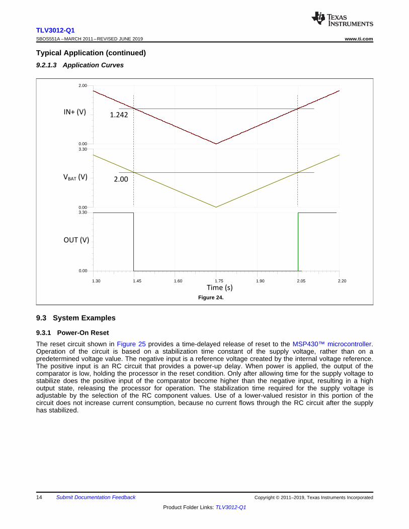
T
Time (s)
1.30 1.45 1.60 1.75 1.90 2.05 2.20
IN
0.00
2.00
VBAT
0.00
3.30
Vout
3.30
1.242
2.00
OUT (V)
IN+ (V)
VBAT (V)
Time (s)
0.00
14
TLV3012-Q1SBOS551A –MARCH 2011–REVISED JUNE 2019 www.ti.com
Product Folder Links: TLV3012-Q1
Submit Documentation Feedback Copyright © 2011–2019, Texas Instruments Incorporated
Typical Application (continued)9.2.1.3 Application Curves
Figure 24.
9.3 System Examples
9.3.1 Power-On ResetThe reset circuit shown in Figure 25 provides a time-delayed release of reset to the MSP430™ microcontroller.Operation of the circuit is based on a stabilization time constant of the supply voltage, rather than on apredetermined voltage value. The negative input is a reference voltage created by the internal voltage reference.The positive input is an RC circuit that provides a power-up delay. When power is applied, the output of thecomparator is low, holding the processor in the reset condition. Only after allowing time for the supply voltage tostabilize does the positive input of the comparator become higher than the negative input, resulting in a highoutput state, releasing the processor for operation. The stabilization time required for the supply voltage isadjustable by the selection of the RC component values. Use of a lower-valued resistor in this portion of thecircuit does not increase current consumption, because no current flows through the RC circuit after the supplyhas stabilized.

V+
F = 724 Hz
V+
2/3 (V+)
1/3 (V+)
R2
1 MΩ
R1
1 MΩ
R2
1 MΩ
R2
1 MΩ
VOUT
VC
V+
t
C
1000 pF
T1 T2
t
TLV3012-Q1
Copyright © 2016, Texas Instruments Incorporated
+
–
V+
R11 MΩDI
C110 nF
1.242 VTLV3012-Q1
MSP430™
RESET
REF
Copyright © 2016, Texas Instruments Incorporated
15
TLV3012-Q1www.ti.com SBOS551A –MARCH 2011–REVISED JUNE 2019
Product Folder Links: TLV3012-Q1
Submit Documentation FeedbackCopyright © 2011–2019, Texas Instruments Incorporated
System Examples (continued)
Figure 25. TLV3012-Q1 Configured as Power-Up Reset Circuit for the MSP430™ Microcontroller
The reset delay needed depends on the power-up characteristics of the system power supply. R1 and C1 areselected to allow enough time for the power supply to stabilize. D1 provides rapid reset if power is lost. In thisexample, the R1 × C1 time constant is 10 ms.
9.3.2 Relaxation OscillatorThe TLV3012-Q1 device can be configured as a relaxation oscillator to provide a simple and inexpensive clockoutput (see Figure 26). The capacitor is charged at a rate of T = 0.69RC and discharges at a rate of 0.69RC.Therefore, the period is T = 1.38RC. R1 may be a different value than R2.
Figure 26. TLV3012-Q1 Configured as Relaxation Oscillator

V-
V+
REF
IN-IN+
GND
OUT
VIN
V
S
GND
GND
OUT
C1
R1R2
SOT-23
16
TLV3012-Q1SBOS551A –MARCH 2011–REVISED JUNE 2019 www.ti.com
Product Folder Links: TLV3012-Q1
Submit Documentation Feedback Copyright © 2011–2019, Texas Instruments Incorporated
10 Power Supply RecommendationsThe TLV3012-Q1 has a recommended operating voltage range (VS) of 1.8 V to 5.5 V. VS is defined as (V+) – (V-). Therefore, the supply voltages used to create VS can be single-ended or bipolar. For example, single-endedsupply voltages of 5 V and 0 V and bipolar supply voltages of +2.5 V and –2.5 V create comparable operatingvoltages for VS. However, when bipolar supply voltages are used, it is important to realize that the reference(REF) and logic low level of the comparator output is referenced to (V-). Output capacitive loading and outputtoggle rate will cause the average supply current to rise over the quiescent current in the EC Table.
11 Layout
11.1 Layout GuidelinesTo minimize supply noise, power supplies should be capacitively decoupled by a 0.1-μF ceramic capacitor.Comparators are sensitive to input noise and precautions such as proper grounding (use of ground plane),supply bypassing, and guarding of high-impedance nodes minimize the effects of noise and help to ensurespecified performance.
11.2 Layout Example
Figure 27. Layout Example

17
TLV3012-Q1www.ti.com SBOS551A –MARCH 2011–REVISED JUNE 2019
Product Folder Links: TLV3012-Q1
Submit Documentation FeedbackCopyright © 2011–2019, Texas Instruments Incorporated
12 Device and Documentation Support
12.1 Receiving Notification of Documentation UpdatesTo receive notification of documentation updates, navigate to the device product folder on ti.com. In the upperright corner, click on Alert me to register and receive a weekly digest of any product information that haschanged. For change details, review the revision history included in any revised document.
12.2 Community ResourcesThe following links connect to TI community resources. Linked contents are provided "AS IS" by the respectivecontributors. They do not constitute TI specifications and do not necessarily reflect TI's views; see TI's Terms ofUse.
TI E2E™ Online Community TI's Engineer-to-Engineer (E2E) Community. Created to foster collaborationamong engineers. At e2e.ti.com, you can ask questions, share knowledge, explore ideas and helpsolve problems with fellow engineers.
Design Support TI's Design Support Quickly find helpful E2E forums along with design support tools andcontact information for technical support.
12.3 TrademarksMSP430, E2E are trademarks of Texas Instruments.All other trademarks are the property of their respective owners.
12.4 Electrostatic Discharge CautionThis integrated circuit can be damaged by ESD. Texas Instruments recommends that all integrated circuits be handled withappropriate precautions. Failure to observe proper handling and installation procedures can cause damage.
ESD damage can range from subtle performance degradation to complete device failure. Precision integrated circuits may be moresusceptible to damage because very small parametric changes could cause the device not to meet its published specifications.
12.5 GlossarySLYZ022 — TI Glossary.
This glossary lists and explains terms, acronyms, and definitions.
13 Mechanical, Packaging, and Orderable InformationThe following pages include mechanical, packaging, and orderable information. This information is the mostcurrent data available for the designated devices. This data is subject to change without notice and revision ofthis document. For browser-based versions of this data sheet, refer to the left-hand navigation.

PACKAGE OPTION ADDENDUM
www.ti.com 10-Dec-2020
Addendum-Page 1
PACKAGING INFORMATION
Orderable Device Status(1)
Package Type PackageDrawing
Pins PackageQty
Eco Plan(2)
Lead finish/Ball material
(6)
MSL Peak Temp(3)
Op Temp (°C) Device Marking(4/5)
Samples
TLV3012AQDCKRQ1 ACTIVE SC70 DCK 6 3000 RoHS & Green NIPDAU Level-1-260C-UNLIM -40 to 125 BPF
(1) The marketing status values are defined as follows:ACTIVE: Product device recommended for new designs.LIFEBUY: TI has announced that the device will be discontinued, and a lifetime-buy period is in effect.NRND: Not recommended for new designs. Device is in production to support existing customers, but TI does not recommend using this part in a new design.PREVIEW: Device has been announced but is not in production. Samples may or may not be available.OBSOLETE: TI has discontinued the production of the device.
(2) RoHS: TI defines "RoHS" to mean semiconductor products that are compliant with the current EU RoHS requirements for all 10 RoHS substances, including the requirement that RoHS substancedo not exceed 0.1% by weight in homogeneous materials. Where designed to be soldered at high temperatures, "RoHS" products are suitable for use in specified lead-free processes. TI mayreference these types of products as "Pb-Free".RoHS Exempt: TI defines "RoHS Exempt" to mean products that contain lead but are compliant with EU RoHS pursuant to a specific EU RoHS exemption.Green: TI defines "Green" to mean the content of Chlorine (Cl) and Bromine (Br) based flame retardants meet JS709B low halogen requirements of <=1000ppm threshold. Antimony trioxide basedflame retardants must also meet the <=1000ppm threshold requirement.
(3) MSL, Peak Temp. - The Moisture Sensitivity Level rating according to the JEDEC industry standard classifications, and peak solder temperature.
(4) There may be additional marking, which relates to the logo, the lot trace code information, or the environmental category on the device.
(5) Multiple Device Markings will be inside parentheses. Only one Device Marking contained in parentheses and separated by a "~" will appear on a device. If a line is indented then it is a continuationof the previous line and the two combined represent the entire Device Marking for that device.
(6) Lead finish/Ball material - Orderable Devices may have multiple material finish options. Finish options are separated by a vertical ruled line. Lead finish/Ball material values may wrap to twolines if the finish value exceeds the maximum column width.
Important Information and Disclaimer:The information provided on this page represents TI's knowledge and belief as of the date that it is provided. TI bases its knowledge and belief on informationprovided by third parties, and makes no representation or warranty as to the accuracy of such information. Efforts are underway to better integrate information from third parties. TI has taken andcontinues to take reasonable steps to provide representative and accurate information but may not have conducted destructive testing or chemical analysis on incoming materials and chemicals.TI and TI suppliers consider certain information to be proprietary, and thus CAS numbers and other limited information may not be available for release.
In no event shall TI's liability arising out of such information exceed the total purchase price of the TI part(s) at issue in this document sold by TI to Customer on an annual basis.
OTHER QUALIFIED VERSIONS OF TLV3012-Q1 :

PACKAGE OPTION ADDENDUM
www.ti.com 10-Dec-2020
Addendum-Page 2
• Catalog: TLV3012
NOTE: Qualified Version Definitions:
• Catalog - TI's standard catalog product

TAPE AND REEL INFORMATION
*All dimensions are nominal
Device PackageType
PackageDrawing
Pins SPQ ReelDiameter
(mm)
ReelWidth
W1 (mm)
A0(mm)
B0(mm)
K0(mm)
P1(mm)
W(mm)
Pin1Quadrant
TLV3012AQDCKRQ1 SC70 DCK 6 3000 179.0 8.4 2.2 2.5 1.2 4.0 8.0 Q3
PACKAGE MATERIALS INFORMATION
www.ti.com 5-Jan-2021
Pack Materials-Page 1

*All dimensions are nominal
Device Package Type Package Drawing Pins SPQ Length (mm) Width (mm) Height (mm)
TLV3012AQDCKRQ1 SC70 DCK 6 3000 200.0 183.0 25.0
PACKAGE MATERIALS INFORMATION
www.ti.com 5-Jan-2021
Pack Materials-Page 2


IMPORTANT NOTICE AND DISCLAIMERTI PROVIDES TECHNICAL AND RELIABILITY DATA (INCLUDING DATASHEETS), DESIGN RESOURCES (INCLUDING REFERENCEDESIGNS), APPLICATION OR OTHER DESIGN ADVICE, WEB TOOLS, SAFETY INFORMATION, AND OTHER RESOURCES “AS IS”AND WITH ALL FAULTS, AND DISCLAIMS ALL WARRANTIES, EXPRESS AND IMPLIED, INCLUDING WITHOUT LIMITATION ANYIMPLIED WARRANTIES OF MERCHANTABILITY, FITNESS FOR A PARTICULAR PURPOSE OR NON-INFRINGEMENT OF THIRDPARTY INTELLECTUAL PROPERTY RIGHTS.These resources are intended for skilled developers designing with TI products. You are solely responsible for (1) selecting the appropriateTI products for your application, (2) designing, validating and testing your application, and (3) ensuring your application meets applicablestandards, and any other safety, security, or other requirements. These resources are subject to change without notice. TI grants youpermission to use these resources only for development of an application that uses the TI products described in the resource. Otherreproduction and display of these resources is prohibited. No license is granted to any other TI intellectual property right or to any third partyintellectual property right. TI disclaims responsibility for, and you will fully indemnify TI and its representatives against, any claims, damages,costs, losses, and liabilities arising out of your use of these resources.TI’s products are provided subject to TI’s Terms of Sale (https:www.ti.com/legal/termsofsale.html) or other applicable terms available eitheron ti.com or provided in conjunction with such TI products. TI’s provision of these resources does not expand or otherwise alter TI’sapplicable warranties or warranty disclaimers for TI products.IMPORTANT NOTICE
Mailing Address: Texas Instruments, Post Office Box 655303, Dallas, Texas 75265Copyright © 2021, Texas Instruments Incorporated


![courses.washington.edu · Op-Amp Comparator Comparator w Schmitt Trigger Adjustable Voltage Divider Digital ... From Trigger Rvpe Carryover Count LED LED Array C] Many Connections](https://static.fdocuments.us/doc/165x107/5e83a15a2d98b205e47d8b9c/op-amp-comparator-comparator-w-schmitt-trigger-adjustable-voltage-divider-digital.jpg)


