TLE4906 Structured book - RS Components
17
January 2009 Sensors Data Sheet V 2.0 TLE4906K / TLE4906L High Precision Hall Effect Switch
Transcript of TLE4906 Structured book - RS Components

January 2009
Sensors
Data Sheet V 2.0
TLE4906K / TLE4906LHigh Precis ion Hal l Ef fect Switch

Edition 2009-01Published by Infineon Technologies AG 81726 Munich, Germany© 2009 Infineon Technologies AG All Rights Reserved.
Legal DisclaimerThe information given in this document shall in no event be regarded as a guarantee of conditions or characteristics. With respect to any examples or hints given herein, any typical values stated herein and/or any information regarding the application of the device, Infineon Technologies hereby disclaims any and all warranties and liabilities of any kind, including without limitation, warranties of non-infringement of intellectual property rights of any third party.
InformationFor further information on technology, delivery terms and conditions and prices, please contact the nearest Infineon Technologies Office (www.infineon.com).
WarningsDue to technical requirements, components may contain dangerous substances. For information on the types in question, please contact the nearest Infineon Technologies Office.Infineon Technologies components may be used in life-support devices or systems only with the express written approval of Infineon Technologies, if a failure of such components can reasonably be expected to cause the failure of that life-support device or system or to affect the safety or effectiveness of that device or system. Life support devices or systems are intended to be implanted in the human body or to support and/or maintain and sustain and/or protect human life. If they fail, it is reasonable to assume that the health of the user or other persons may be endangered.
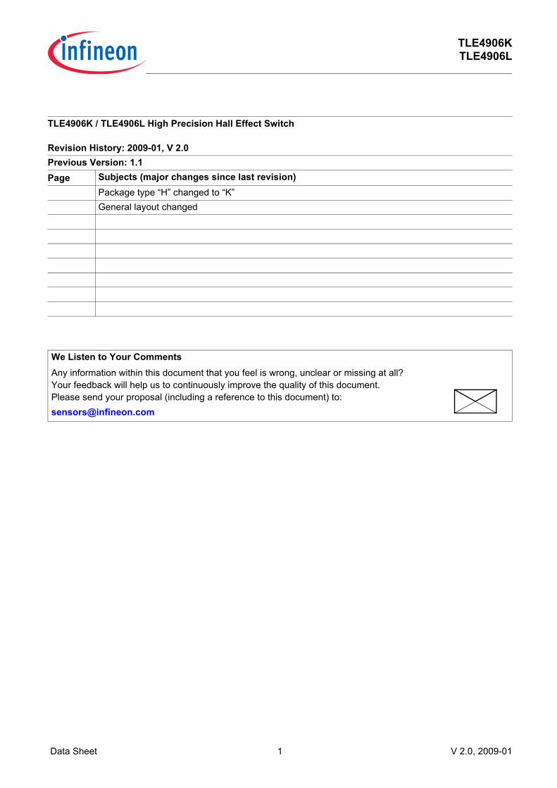
TLE4906K / TLE4906L High Precision Hall Effect Switch Revision History: 2009-01, V 2.0Previous Version: 1.1Page Subjects (major changes since last revision)
Package type “H” changed to “K”General layout changed
We Listen to Your CommentsAny information within this document that you feel is wrong, unclear or missing at all? Your feedback will help us to continuously improve the quality of this document. Please send your proposal (including a reference to this document) to:[email protected]
Data Sheet 1 V 2.0, 2009-01
TLE4906KTLE4906L

TLE4906KTLE4906L
Table of Contents
Data Sheet 2 V 2.0, 2009-01
1 Product Description 31.1 Overview 31.2 Features 31.3 Target Applications 3
2 Functional Description 42.1 General 42.2 Pin Configuration (top view) 42.3 Pin Description 42.4 Block Diagram 52.5 Functional Block Description 5
3 Specification 73.1 Absolute Maximum Ratings 73.2 Operating Range 83.3 Electrical and Magnetic Characteristics 9
4 Package Information 114.1 Package Outline 114.2 Distance between Chip and Package 134.3 Package Marking 13
Table of Contents

High Precision Hall-Effect Switch
TLE4906KTLE4906L
1 Product Description
1.1 OverviewThe TLE4906 is a high precision Hall effect switch with highly accurate switching thresholds for operating temperatures up to 150°C.
1.2 Features
• 2.7V to 24V supply voltage• Operation from unregulated power supply• High sensitivity and high stability of the magnetic switching points• High resistance to mechanical stress by Active Error Compensation• Reverse battery protection (-18V)• Superior temperature stability• Peak temperatures up to 195°C without damage• Low jitter (typ. 1µs)• High ESD performance (± 6kV HBM)• Digital output signal• SMD package SC59 (SOT23 compatible) - (TLE4906K))• Leaded package PG-SSO-3-2 - (TLE4906L)
1.3 Target ApplicationsTarget applications for TLE4906 are all automotive applications which require a high precision Hall switch for position sensing with a operating temperature range from -40°C to +150°C.
Product Name Product Type Ordering Code PackageHall Effect Switch TLE4906K SP000475028 SC59Hall Effect Switch TLE4906L SP000012949 PG-SSO-3-2
Data Sheet 3 V 2.0, 2009-01

TLE4906KTLE4906L
Functional Description
2 Functional Description
2.1 GeneralThe TLE4906K and the TLE4906L are integrated circuit Hall-effect sensors designed specifically for highly accurate applications.Precise magnetic switching points and high temperature stability are achieved by active compensation circuits and chopper techniques on chip.
2.2 Pin Configuration (top view)
Center ofSensitive Area
1± 0.151.5
± 0.150.8
2
3
321PG-SSO-3-2SC59
± 0.11.35
± 0.12.08
Figure 1 Pin Configuration and Center of Sensitive Area
2.3 Pin Description
Table 1 Pin Description SC59 Pin No. Symbol Function Comment1 VS Supply voltage2 Q Output3 GND Ground
Table 2 Pin Description PG-SSO-3-2 Pin No. Symbol Function Comment1 VS Supply voltage2 GND Ground3 Q Output
Data Sheet 4 V 2.0, 2009-01

TLE4906KTLE4906L
Functional Description
2.4 Block Diagram
Ref
ChoppedHall Probe
VS
Q
GNDAmplifier Low Pass Filter
Comparator with
Hysteresis
Voltage Regulatorreverse polarity protected
Oscillatorand
Sequencer
Bias andCompensation
Circuits
Figure 2 Functional Block Diagram
2.5 Functional Block DescriptionThe chopped Hall IC Switch comprises a Hall probe, bias generator, compensation circuits, oscillator and output transistor.The bias generator provides currents for the Hall probe and the active circuits. Compensation circuits stabilize the temperature behavior and reduce technology variations.The Active Error Compensation rejects offsets in signal stages and the influence of mechanical stress to the Hall probe caused by molding and soldering processes and other thermal stresses in the package.This chopper technique together with the threshold generator and the comparator ensure high accurate magnetic switching points. .
Data Sheet 5 V 2.0, 2009-01

TLE4906KTLE4906L
Functional Description
AppliedMagneticField
90%
10%
VQ
tf
tdtr
td
BOP
BRP
Figure 3 Timing Diagram
VQ
BopBrp0B
Figure 4 Output Signal
Data Sheet 6 V 2.0, 2009-01

TLE4906KTLE4906L
Specification
3 Specification
3.1 Absolute Maximum Ratings
Table 3 Absolute Maximum Rating Parameters Tj = -40°C to 150°C
Parameter Symbol Limit Values Unit Note / Test ConditionMin. Max.
Supply voltage VS -18-18-18
182426
Vfor 1h, RS ≥ 200Ωfor 5min, RS ≥ 200Ω
Supply current through protection device
IS -50 50 mA
Output voltage VQ -0.7-0.7
1826
Vfor 5min @ 1.2kΩ pull up
Continuous output current IQ -50 50 mAJunction temperature Tj –
– – –
155 165 175 195
°C for 2000h (not additive) for 1000h (not additive) for 168h (not additive) for 3 x 1h (additive)
Storage temperature TS -40 150 °CMagnetic flux density B – unlimited mT
Note: Stresses above the max. values listed here may cause permanent damage to the device. Exposure to absolute maximum rating conditions for extended periods may affect device reliability. Maximum ratings are absolute ratings; exceeding only one of these values may cause irreversible damage to the integrated circuit.
Table 4 ESD Protection1)
1) Human Body Model (HBM) tests according to: EOS/ESD Association Standard S5.1-1993 and Mil. Std. 883D method 3015.7
Parameter Symbol Limit Values Unit Note / Test ConditionMin. Max.
ESD Voltage VESD ±6 kV HBM, R = 1.5kΩ, C = 100pF TA = 25°C
Data Sheet 7 V 2.0, 2009-01

TLE4906KTLE4906L
Specification
3.2 Operating Range
Table 5 Operating Conditions Parameters Parameter Symbol Values Unit Note / Test Condition
Min. Typ. Max.Supply voltage VS 2.7 18 VOutput voltage VQ -0.7 18 VJunction temperature Tj -40 150 °C
Output current IQ 0 20 mA
The following operating conditions must not be exceeded in order to ensure correct operation of the TLE4906K / TLE4906L.All parameters specified in the following sections refer to these operating conditions unless otherwise mentioned.
Data Sheet 8 V 2.0, 2009-01
TLE4906KTLE4906L
Specification
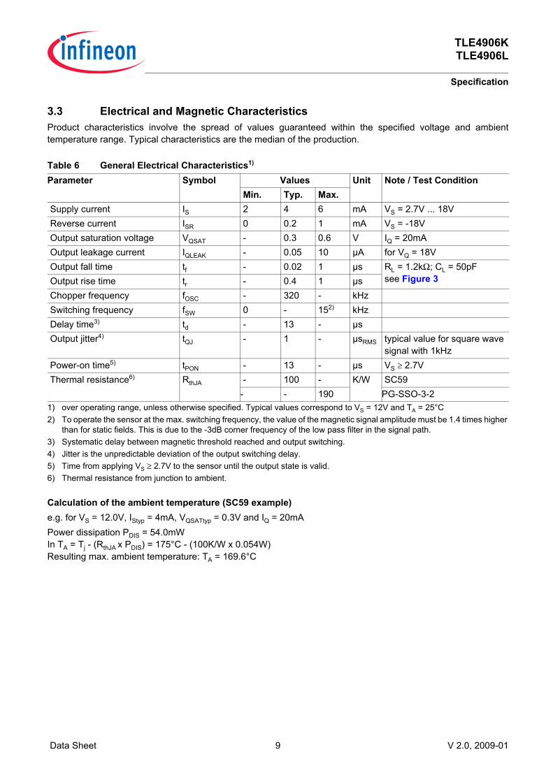
3.3 Electrical and Magnetic Characteristics
Table 6 General Electrical Characteristics1)
1) over operating range, unless otherwise specified. Typical values correspond to VS = 12V and TA = 25°C
Parameter Symbol Values Unit Note / Test Condition
Min. Typ. Max.Supply current IS 2 4 6 mA VS = 2.7V ... 18VReverse current ISR 0 0.2 1 mA VS = -18VOutput saturation voltage VQSAT - 0.3 0.6 V IQ = 20mAOutput leakage current IQLEAK - 0.05 10 µA for VQ = 18VOutput fall time tf - 0.02 1 µs RL = 1.2kΩ; CL = 50pF
see Figure 3Output rise time tr - 0.4 1 µsChopper frequency fOSC - 320 - kHzSwitching frequency fSW 0 -
2) To operate the sensor at the max. switching frequency, the value of the magnetic signal amplitude must be 1.4 times higher than for static fields. This is due to the -3dB corner frequency of the low pass filter in the signal path.
152) kHzDelay time
3) Systematic delay between magnetic threshold reached and output switching.
3) td - 13 - µsOutput jitter
4) Jitter is the unpredictable deviation of the output switching delay.
4) tQJ - 1 - µsRMS typical value for square wave signal with 1kHz
Power-on time
5) Time from applying VS ≥ 2.7V to the sensor until the output state is valid.
5) tPON - 13 - µs VS ≥ 2.7VThermal resistance
6) Thermal resistance from junction to ambient.
6) RthJA - 100 - K/W SC59- - 190 PG-SSO-3-2
Product characteristics involve the spread of values guaranteed within the specified voltage and ambient temperature range. Typical characteristics are the median of the production.
Calculation of the ambient temperature (SC59 example)e.g. for VS = 12.0V, IStyp = 4mA, VQSATtyp = 0.3V and IQ = 20mAPower dissipation PDIS = 54.0mW In TA = Tj - (RthJA x PDIS) = 175°C - (100K/W x 0.054W) Resulting max. ambient temperature: TA = 169.6°C
Data Sheet 9 V 2.0, 2009-01

TLE4906KTLE4906L
Specification
Table 7 Magnetic Characteristics1)
1) over operating range, unless otherwise specified. Typical values correspond to VS = 12V and TA = 25°C.
Parameter Symbol Tj[°C] Values Unit Note / Test ConditionMin. Typ. Max.
Operating point BOP -4025150
6.76.56.2
10.310.09.5
13.913.512.9
mT
Release point BRP -4025150
5.25.04.7
8.78.58.1
12.312.011.4
mT
Hysteresis BHYS -4025150
-0.7-
-1.5-
-3.0-
mT
Temperature compensation of magnetic thresholds
TC - -350 - ppm/°C
Repeatability of magnetic thresholds
2) BREP is equivalent to the noise constant
2)BREP - 20 - µTRMS typ. value for
∆B/∆t > 12mT/ms
Note: Typical characteristics specify mean values expected over the production spread
Branded Side
N
S
N
S Branded Side
Field Direction DefinitionPositive magnetic fields are defined with the south pole of the magnet to the branded side of package.
Figure 5 Definition of magnetic field direction (left: SC59, right: PG-SSO-3-2)
Data Sheet 10 V 2.0, 2009-01

TLE4906KTLE4906L
Package Information
4 Package Information
4.1 Package Outline
3x0.4 +0.05-0.1
M0.1
0.95
0.95
(0.55)
3±0.1
+0.2
2.8
-0.1
0.15 MAX.
1.1 ±0.1
0.2 +0.1
+0.1-0.05
0.15
0˚...8˚ MAX.
GPS09473
0.45
±0.1
5
+0.1
5-0
.31.
6
0.1
M
0.1
3
21
Figure 6 SC59 Package Outline (all dimensions in mm)
Reflow Soldering Wave Soldering
0.8
0.8
1.2
0.9
1.3
0.9
0.8
0.8
1.2
1.6
1.4
min
1.4
min
The following picture shows a recommendation for the PCB layout.
Figure 7 SC59 Footprint (SOT23 compatible, all dimensions in mm)
Data Sheet 11 V 2.0, 2009-01

TLE4906KTLE4906L
Package Information
Total tolerance at 10 pitches ±11) No solder func tion area
±0.3
±0.46.3512.7
12.7±1
±0.5
-0.5
+0.7
5
4 ±0.3
9
GP O05358
-0.15
±0.1
Tape
Adhes iveTape
0.250.39
±0.5
A
18
6
23.8
±0.5
38 M
AX.
-111 32
1.27±0.25
1.27±0.25
0.6 MAX.
0.4±0.05
1)1
MAX
.
0.15
MAX
.
1 .9 MAX.4.06±0.08
4.16±0.05
±0.0
83.
293±
0.06
0.2
(0.2
5)
x 45°0.8±0.1
7°
x 45°
±0
.10.
350.2+0.1
7°
(0.79)
A21.52±0.05
Figure 8 PG-SSO-3-2 Package Outline (All dimensions in mm)
Data Sheet 12 V 2.0, 2009-01

TLE4906KTLE4906L
Package Information
4.2 Distance between Chip and Package
PG-SSO-3-2 : 0.57d : Distance chip to upper side of IC
mm±0.08
AEA02510-1
Hall-Probe
Branded Side
d
Figure 9 Distance between chip and package PG-SSO-3-2
AEA03244
Branded Side
d: Distance chip to upper side of IC SC59:
d
0.56 ±0.1 mm
Figure 10 Distance between chip and package SC59
4.3 Package Marking
AEA03641
06Year (y) = 0...9Month (m) = 1...9,
O - OctoberN - NovemberD - December
y m
Figure 11 Marking of TLE4906K
Data Sheet 13 V 2.0, 2009-01

TLE4906KTLE4906L
Package Information
Year (y) = 0...9Calendar Week (ww) = 01...52
yww
06L
S
Figure 12 Marking of TLE4906L
Data Sheet 14 V 2.0, 2009-01