TLC5958 48-Channel, 16-Bit ES-PWM LED Driver with Pre ...
30
X 48 COM n COM 1 COM 0 SW COM 1 VLED SW COM 0 SW COM n VLED VLED COMSEL n COMSEL 1 COMSEL 0 OUTR0 GCLK FLAGS READ LAT SCLK DATA Controller 3 ICn IC1 TLC5958 TLC5958 SIN SCLK LAT GCLK IREF GND OUTR0 OUTB15 SOUT Thermal Pad VCC GND IREFGND SIN SCLK LAT GCLK GND IREFGND IREF OUTB15 SOUT Thermal Pad VCC VCC GND X 48 VCC Product Folder Sample & Buy Technical Documents Tools & Software Support & Community TLC5958 SLVSCE7A – MAY 2014 – REVISED SEPTEMBER 2014 TLC5958 48-Channel, 16-Bit ES-PWM LED Driver with Pre-Charge FET, LED Open Detection and Display Data Memory Support 32-Multiplexing 1 Features 2 Applications 1• 48 Channels Constant Current Sink Output • LED Video Displays with Multiplexing System • Sink Current Capability with Max BC/CC data: • LED Signboards with Multiplexing system • High Refresh Rate & High density LED Panel – 25mA at 5VCC – 20mA at 3.3VCC 3 Description • Global Brightness Control (BC) : 3-Bit (8 Step) The TLC5958 is a 48 channels constant-current sink • Color Brightness Control (CC) for Each Color driver for multiplexing system with 1 to 32 duty ratio. Group: Each channel has an individually-adjustable, 65536- 9-Bit (512 Step), Three Groups step, pulse width modulation (PWM) grayscale (GS). • Grayscale(GS) Control with Multiplexed Enhanced 48K bit display memory is implemented to increase Spectrum(ES) PWM: 16bit the visual refresh rate and to decrease the GS data • 48K bit Grayscale Data Memory Support 32- writing frequency. multiplexing The output channels are grouped into three groups, • LED Power Supply Voltage Up To 10V each group has 16 channels. Each group has a 512- • Vcc = 3.0V to 5.5V step color brightness control (CC) function. The maximum current value of all 48 channels can be set • Constant Current Accuracy by 8-step global brightness control (BC) function. CC – Channel to Channel = ±1%(Typ), ±3%(Max) and BC can be used to adjust the brightness – Device to Device = ±1%(Typ), ±2%(Max) deviation between LED drivers. GS, CC, and BC data are accessible via a serial interface port. • Data Transfer Rate: 25MHz • Gray Scale Clock: 33MHz Send request via email for Application Note: Build High Density, High Refresh Rate, Multiplexing LED • LED Open Detection (LOD) Panel with TLC5958. • Thermal Shut Down (TSD) • I REF Resistor Short Protection (ISP) Device Information(1) • Power-Save Mode (PSM) with high speed PART NUMBER PACKAGE BODY SIZE (NOM) recovery TLC5958 VQFN (56) 8.00 mm × 8.00 mm • Delay Switching to Prevent Inrush Current (1) For all available packages, see the orderable addendum at the end of the datasheet. • Pre-charge FET to Avoid Ghosting Phenomenon • Operating Temperature : –40°C to +85°C 4 Typical Application Circuit (Multiple Daisy-Chained TLC5958s) 1 An IMPORTANT NOTICE at the end of this data sheet addresses availability, warranty, changes, use in safety-critical applications, intellectual property matters and other important disclaimers. PRODUCTION DATA.
Transcript of TLC5958 48-Channel, 16-Bit ES-PWM LED Driver with Pre ...

X 48
COM n
COM 1
COM 0
SW
COM 1
VLED
SW
COM 0
SW
COM n
VLED
VLED
CO
MS
EL
n
CO
MS
EL
1
CO
MS
EL
0
OUTR0
GCLK
FLAGS
READ
LAT
SCLK
DATA
Controller
3
ICnIC1
TLC5958 TLC5958
SIN
SCLK
LAT
GCLK
IREF
GND
OUTR0 OUTB15
SOUT
Thermal
Pad
VCC
GND
IREFGND
SIN
SCLK
LAT
GCLK
GND
IREFGND
IREF
OUTB15
SOUT
Thermal
Pad
VCC
VCC
GND
X 48
VCC
Product
Folder
Sample &Buy
Technical
Documents
Tools &
Software
Support &Community
TLC5958SLVSCE7A –MAY 2014–REVISED SEPTEMBER 2014
TLC5958 48-Channel, 16-Bit ES-PWM LED Driver with Pre-Charge FET, LED OpenDetection and Display Data Memory Support 32-Multiplexing
1 Features 2 Applications1• 48 Channels Constant Current Sink Output • LED Video Displays with Multiplexing System• Sink Current Capability with Max BC/CC data: • LED Signboards with Multiplexing system
• High Refresh Rate & High density LED Panel– 25mA at 5VCC– 20mA at 3.3VCC
3 Description• Global Brightness Control (BC) : 3-Bit (8 Step)The TLC5958 is a 48 channels constant-current sink• Color Brightness Control (CC) for Each Color driver for multiplexing system with 1 to 32 duty ratio.
Group: Each channel has an individually-adjustable, 65536-9-Bit (512 Step), Three Groups step, pulse width modulation (PWM) grayscale (GS).
• Grayscale(GS) Control with Multiplexed Enhanced 48K bit display memory is implemented to increaseSpectrum(ES) PWM: 16bit the visual refresh rate and to decrease the GS data• 48K bit Grayscale Data Memory Support 32- writing frequency.
multiplexing The output channels are grouped into three groups,• LED Power Supply Voltage Up To 10V each group has 16 channels. Each group has a 512-• Vcc = 3.0V to 5.5V step color brightness control (CC) function. The
maximum current value of all 48 channels can be set• Constant Current Accuracyby 8-step global brightness control (BC) function. CC– Channel to Channel = ±1%(Typ), ±3%(Max) and BC can be used to adjust the brightness
– Device to Device = ±1%(Typ), ±2%(Max) deviation between LED drivers. GS, CC, and BC dataare accessible via a serial interface port.• Data Transfer Rate: 25MHz
• Gray Scale Clock: 33MHz Send request via email for Application Note: BuildHigh Density, High Refresh Rate, Multiplexing LED• LED Open Detection (LOD)Panel with TLC5958.• Thermal Shut Down (TSD)
• IREF Resistor Short Protection (ISP) Device Information(1)• Power-Save Mode (PSM) with high speed PART NUMBER PACKAGE BODY SIZE (NOM)
recovery TLC5958 VQFN (56) 8.00 mm × 8.00 mm• Delay Switching to Prevent Inrush Current (1) For all available packages, see the orderable addendum at
the end of the datasheet.• Pre-charge FET to Avoid Ghosting Phenomenon• Operating Temperature : –40°C to +85°C
4 Typical Application Circuit (Multiple Daisy-Chained TLC5958s)
1
An IMPORTANT NOTICE at the end of this data sheet addresses availability, warranty, changes, use in safety-critical applications,intellectual property matters and other important disclaimers. PRODUCTION DATA.
TLC5958SLVSCE7A –MAY 2014–REVISED SEPTEMBER 2014 www.ti.com
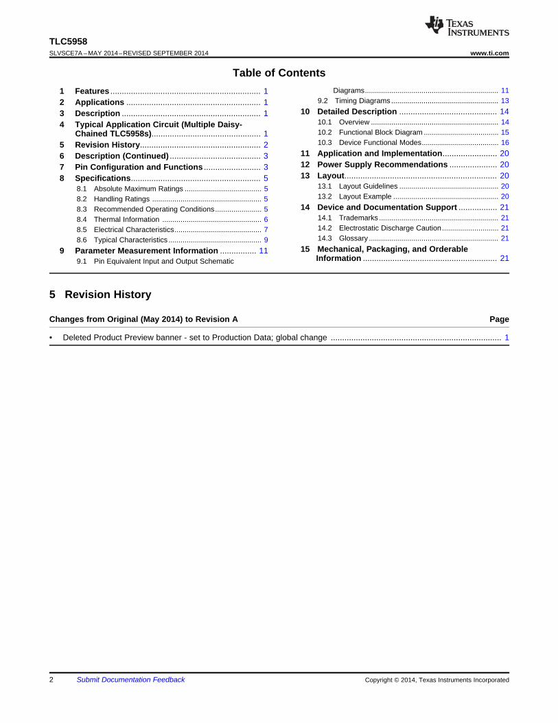
Table of ContentsDiagrams.................................................................. 111 Features .................................................................. 1
9.2 Timing Diagrams..................................................... 132 Applications ........................................................... 110 Detailed Description ........................................... 143 Description ............................................................. 1
10.1 Overview ............................................................... 144 Typical Application Circuit (Multiple Daisy-10.2 Functional Block Diagram ..................................... 15Chained TLC5958s)................................................ 110.3 Device Functional Modes...................................... 165 Revision History..................................................... 2
11 Application and Implementation........................ 206 Description (Continued) ........................................ 312 Power Supply Recommendations ..................... 207 Pin Configuration and Functions ......................... 313 Layout................................................................... 208 Specifications......................................................... 5
13.1 Layout Guidelines ................................................. 208.1 Absolute Maximum Ratings ...................................... 513.2 Layout Example .................................................... 208.2 Handling Ratings ...................................................... 5
14 Device and Documentation Support ................. 218.3 Recommended Operating Conditions....................... 514.1 Trademarks ........................................................... 218.4 Thermal Information ................................................. 614.2 Electrostatic Discharge Caution............................ 218.5 Electrical Characteristics........................................... 714.3 Glossary ................................................................ 218.6 Typical Characteristics .............................................. 9
15 Mechanical, Packaging, and Orderable9 Parameter Measurement Information ................ 11Information ........................................................... 219.1 Pin Equivalent Input and Output Schematic
5 Revision History
Changes from Original (May 2014) to Revision A Page
• Deleted Product Preview banner - set to Production Data; global change ........................................................................... 1
2 Submit Documentation Feedback Copyright © 2014, Texas Instruments Incorporated

RTQ
(TOP VIEW)
ThermalPAD
(Solder side)
(GND terminal)
15 16 17 18 19 20 21 22
52 51 50 49
42
41
40
39
38
37
56 55 54 53
1
2
3
4
5
6
7
8
SOUT
OUTB9
OUTG9
OUTR9
OUTB8
OUTG8
OUTR8
OUTB7
OUTG7
OUTR7
OUTB6
OUTG6
OUTR6
GCLK
IRE
FG
ND
OU
TB
13
OU
TG
13
OU
TR
13
OU
TB
12
OU
TG
12
OU
TR
12
OU
TB
11
OU
TG
11
OU
TR
11
OU
TB
10
OU
TG
10
OU
TR
10
VC
C
OU
TG
2
OU
TB
2
OU
TR
3
OU
TG
3
OU
TB
3
OU
TR
4
OU
TG
4
OU
TB
4
OU
TR
5
OU
TG
5
OU
TB
5
SIN
LA
T
SC
LK
IREF
OUTR14
OUTG14
OUTB14
OUTR15
OUTG15
OUTB15
OUTR0
OUTG0
OUTB0
OUTR1
OUTG1
OUTB1
OUTR2
36
35
34
33
32
31
30
29
9
10
11
12
13
14
23 24 25 26 27 28
48 47 46 45 44 43
TLC5958www.ti.com SLVSCE7A –MAY 2014–REVISED SEPTEMBER 2014
6 Description (Continued)The TLC5958 has one error flag: LED open detection (LOD), which can be read via a serial interface port. TheTLC5958 also has a power-save mode that sets the total current consumption to 0.8mA (typ) when all outputsare off.
7 Pin Configuration and Functions
56 Pin
Pin FunctionsPIN
I/O DESCRIPTIONNAME NO.
Grayscale(GS) pulse width modulation (PWM) reference clock control for OUTXn.GCLK 29 I Each GCLK rising edge increase the GS counter by1 for PWM control.GND ThermalPad – Power ground. The thermal pad must be soldered to GND on PCB.
Maximum constant-current value setting. The OUTR0 to OUTB15 maximum constant outputcurrent are set to the desired values by connecting an external resistor between IREF andIREF 1 – IREFGND. See equation 1 for more detail. The external resistor should be placed close tothe device.Analog ground. Dedicated ground pin for the external IREF resistor. This pin should be
IREFGND 56 – connected to analog ground trace which is connected to power ground near the commonGND point of board.The LAT falling edge latches the data from the common shift register into the GS dataLAT 27 I memory or Function control(FC) register FC1 or FC2.
8, 11, 14, 17,20, 23, 30, Constant current output for RED LED. Multiple outputs can be tied together to increase the
OUTR0-R15 33, 36, 39, O constant current capability. Different voltages can be applied to each output. These outputs44, 47, 50, are turned on-off by GCLK signal and the data in GS data memory.
53 ,2, 5
Copyright © 2014, Texas Instruments Incorporated Submit Documentation Feedback 3

TLC5958SLVSCE7A –MAY 2014–REVISED SEPTEMBER 2014 www.ti.com
Pin Functions (continued)PIN
I/O DESCRIPTIONNAME NO.
9, 12, 15, 18,21, 24, 31, Constant current output for GREEN LED. Multiple outputs can be tied together to increase
OUTG0-G15 34, 37, 40, O the constant current capability. Different voltages can be applied to each output. These45, 48, 51, outputs are turned on-off by GCLK signal and the data in GS data memory.
54, 3, 610, 13, 16,19, 22, 25, Constant current output for BLUE LED. Multiple outputs can be tied together to increase the
OUTB0-B15 32, 35, 38, O constant current capability. Different voltages can be applied to each output. These outputs41, 46, 49, are turned on-off by GCLK signal and the data in GS data memory.52, 55, 4, 7
Serial data shift clock. Data present on SIN are shifted to the 48-bit common shift registerSCLK 28 I LSB with the SCLK rising edge. Data in the shift register are shifted towards the MSB at
each SCLK rising edge. The common shift register MSB appears on SOUT.Serial data input of the 48-bit common shift register. When SIN is high level, the LSB is setto '1' for only one SCLK input rising edge. If two SCLK rising edges are input while SIN isSIN 26 I high, then the 48-bit shift register LSB and LSB+1 are set to '1'. When SIN is low, the LSB isset to '0' at the SCLK input rising edge.Serial data output of the 48-bit common shift register. SOUT is connected to the MSB of theSOUT 42 O register.
VCC 43 – Power-supply voltage.
4 Submit Documentation Feedback Copyright © 2014, Texas Instruments Incorporated

TLC5958www.ti.com SLVSCE7A –MAY 2014–REVISED SEPTEMBER 2014
8 Specifications
8.1 Absolute Maximum Ratingsover operating free-air temperature range (unless otherwise noted) (1)
PARAMETER MIN MAX UNITVCC
(2) Supply voltage VCC 0.3 6.0 VIOUT Output current (dc) OUTx0 to OUTx15, x=R, G, B 30 mAVIN
(2) Input voltage SIN, SCLK, LAT, GCLK, IREF –0.3 VCC+0.3 VSOUT –0.3 VCC+0.3
VOUT(2) Output voltage V
OUTx0 to OUTx15, x=R, G, B –0.3 11TJ(MAX) Operating junction temperature 150 °C
(1) Stresses beyond those listed under Absolute Maximum Ratings may cause permanent damage to the device. These are stress ratingsonly, which do not imply functional operation of the device at these or any other conditions beyond those indicated under RecommendedOperating Conditions. Exposure to absolute-maximum-rated conditions for extended periods may affect device reliability.
(2) All voltage values are with respect to device ground terminal.
8.2 Handling RatingsMIN MAX UNIT
Tstg Storage temperature range –55 150 °CHuman body model (HBM), per ANSI/ESDA/JEDEC JS-001, all 0 4000pins (2)ElectrostaticV(ESD)
(1) Vdischarge Charged device model (CDM), per JEDEC specification 0 1000JESD22-C101, all pins (3)
(1) Electrostatic discharge (ESD) measures device sensitivity and immunity to damage caused by assembly line electrostatic dischargesinto the device.
(2) Level listed above is the passing level per ANSI, ESDA, and JEDEC JS-001. JEDEC document JEP155 states that 500-V HBM allowssafe manufacturing with a standard ESD control process.
(3) Level listed above is the passing level per EIA-JEDEC JESD22-C101. JEDEC document JEP157 states that 250-V CDM allows safemanufacturing with a standard ESD control process.
8.3 Recommended Operating ConditionsAt TA = –40°C to +85°C, unless otherwise noted
MIN NOM MAX UNITDC CHARACTERISTICS, VCC=3V to 5.5VVCC Supply voltage 3 5.5 VVO Voltage applied to output OUTx0 to OUTx15, x=R, G, B 10 VVIH High level input voltage SIN,SCLK,LAT,GCLK 0.7×VCC VCC VVIL Low level input voltage SIN,SCLK,LAT,GCLK GND 0.3×VCC VIOH High level output current SOUT -2 mAIOL Low level output current SOUT 2 mA
OUTx0 to OUTx15, x=R, G, B, 203V ≤ VCC ≤ 3.6VIOLC Constant output sink current mA
OUTx0 to OUTx15, x=R, G, B, 254V < VCC ≤ 5.5VTA Operating free air temperature –40 85 °CTJ Operation junction temperature -40 125 °C
Copyright © 2014, Texas Instruments Incorporated Submit Documentation Feedback 5

TLC5958SLVSCE7A –MAY 2014–REVISED SEPTEMBER 2014 www.ti.com
Recommended Operating Conditions (continued)At TA = –40°C to +85°C, unless otherwise noted
MIN NOM MAX UNITAC CHARACTERISTICS, VCC=3V to 5.5V (1)
FCLK(SCLK) Data shift clock frequency SCLK 25 MHzFCLK(GCLK) Grayscale control clock frequency GCLK 33 MHztWH0 SCLK 10tWL0 SCLK 10
Pulse duration nstWH1 GCLK 15tWL1 GCLK 10tSU0 SIN - SCLK↑ 2tSU1 LAT↑ - SCLK↑ 3
LAT↓ - SCLK↑ 5 nstSU2 LAT↓ - SCLK↑, for READSID, READFC1, 50and READFC2Setup timetSU3 LAT↓ (Vsync command) - GCLK↑ 2500
The last LAT↓ for no all ‘0’ data latching totSU4 resume normal mode – GCLK↑, 50 µS
PSAVE_ENA bit = ‘1b’tSU5 The last GCLK↑ - the 1st GCLK↑ of next line 20 nstH0 SCLK↑ - SIN 2tH1 Hold time SCLK↑ - LAT↑ 2 nstH2 SCLK↑ - LAT↓ 13
(1) Specified by design
8.4 Thermal InformationTLC5958
THERMAL METRIC (1) RTQ UNIT56 PINS
RθJA Junction-to-ambient thermal resistance 27.4RθJC(top) Junction-to-case (top) thermal resistance 13.6RθJB Junction-to-board thermal resistance 5.5
°C/WψJT Junction-to-top characterization parameter 0.2ψJB Junction-to-board characterization parameter 5.5RθJC(bot) Junction-to-case (bottom) thermal resistance 0.8
(1) For more information about traditional and new thermal metrics, see the IC Package Thermal Metrics application report, SPRA953.
6 Submit Documentation Feedback Copyright © 2014, Texas Instruments Incorporated

( ) ( )( )
(IOUTXn at VOUTXn 3V) – IOUTXn at VOUTXn 1V 100%V
IOUTXn at VOUTXn 1V 3V – 1V
é ù= =D = ´ê ú
=ê úë û
( ) ( )( )
(IOUTXn at VCC 5.5V) – IOUTXn at VCC 3.0V 100%V
IOUTXn at VCC 3.0V 5.5V – 3V
é ù= =D = ´ê ú
=ê úë û
( ) ( ) ( )IREF
IREF
VI deal Output mA Gain CCR or CCG, CCB /511d, VIREF 1.209V Typ ,
R ( )
Refer to Table 1 for the Gain at chosen BC.
é ù= ´ ´ =ê ú
Wê úë û
( )(IOUTX0 IOUTX1 IOUTX15)
(Ideal Output Current)16% 100
Ideal Output Current
+ + ¼ +é ù-ê ú
D = ´ê úê úê úë û
( ) IOUTXn% 1 100
(IOUTX0 IOUTX1 IOUTX14 IOUTX15)
16
é ùê ú
D = - ´ê ú+ + ¼ + +ê ú
ê úë û
Ideal current is calculated by the following equation:
TLC5958www.ti.com SLVSCE7A –MAY 2014–REVISED SEPTEMBER 2014
8.5 Electrical CharacteristicsAt VCC= 3.0V to 5.5V and TA= –40°C to 85°C, VLED=5.0V, Typical values are at VCC= 3.3V, TA= 25°C (unless otherwisenoted).
PARAMETER TEST CONDITIONS MIN TYP MAX UNIT
VOH High IOH = -2mA at SOUT VCC–0.4 VCC VOutput voltage
VOL Low IOL= 2 mA at SOUT 0.4 V
VLOD0 LODVTH = 00b 0.06 0.11 0.16
VLOD1 LODVTH = 01b 0.2 0.25 0.3LED open detection threshold V
VLOD2 LODVTH = 10b 0.34 0.39 0.44
VLOD3 LODVTH = 11b 0.44 0.49 0.54
VIREF Reference voltage output RIREF = 6.2 kΩ (1mA target), BC=0h, CCR/G/B=81h 1.19 1.209 1.228 V
IIN Input current (SIN, SCLK) VIN = VCC or GND –1 1 µA
SIN/SCLK/LAT/GSCLK=GND, GSn=0000h, BC=0h, 5.5 7ICC0 CCR/G/B=81h, VOUTn = Vcc, RIREF=OPEN
SIN/SCLK/LAT/GSCK=GND, GSn=0000h, BC=4h, 7 9ICC1 CCR/G/B=137h,VOUTn=Vcc, RIREF=7.5kΩ (Io=10mA target)
SIN/SCLK/LAT=GND, GCLK=33MHz, TSU5 = 200nS, 25 318+8 mode, GSn=FFFFh, BC=4h, CCR/G/B=137h,ICC2 Supply current (Vcc) VOUTn=Vcc-1V when channel on, VOUTn=Vcc mAwhen channel off. RIREF=7.5kΩ (Io=10mA target)
SIN/SCLK/LAT=GND, GCLK=33MHz, TSU5=200nS, 28 338+8 mode, GSn=FFFFh, BC=7h, CCR/G/B=1F5h,ICC3 VOUTn=Vcc-2.5V when channel on, VOUTn=Vccwhen channel off. RIREF=7.5kΩ (Io=25mA target)
ICC4 In power save mode 0.9 1.5
All OUTn=on, BC=0h, CCR/G/B=81h, VOUTn=VOUTfix=1V, ±1% ±3%Constant current error Channel-to-ΔIOLC0 RIREF=6.2kΩ(1mA target), TA = +25°C, at same colorchannel (1)(OUTx0-15, x=R/G/B) grouped output of OUTR0-15, OUTG0-15 and OUTB0-15
All OUTn=on, BC=0h, CCR/G/B=81h, VOUTn=VOUTfix=1V, ±1% ±2%Constant current error Device-to-ΔIOLC1 RIREF=6.2kΩ(1mA target), TA =+25°C, at same colordevice (2)(OUTx0-15, x=R/G/B) grouped output of OUTR0-15, OUTG0-15 and OUTB0-15
VCC=3.0 to 5.5V, All OUTn=on, BC=0h, CCR/G/B=81h,ΔIOLC2 Line regulation (3) ±1 ±1.5 %/VVOUTn=VOUTfix=1V, RIREF=6.2kΩ (1mA target)
All OUTn=on, BC=0h, CCR/G/B=81h, VOUTn=1 to 3V,ΔIOLC3 Load regulation (4) ±1 ±1.5 %/VVOUTfix=1V, RIREF=6.2kΩ (1mA target)
(1) The deviation of each outputs in same color group (OUTR0~15 or OUTG0~15 or OUTB0~15) from the average of same color groupconstant current. The deviation is calculated by the formula. (X=R or G or B, n=0~15)
spacer(2) The deviation of the average of constant-current in each color group from the ideal constant-current value. (X = R or G or B) :
spacer(3) Line regulation is calculated by the following equation. (X=R or G or B, n=0~15):
spacer(4) Load regulation is calculated by the following equation. (X=R or G or B, n=0~15):
spacer
Copyright © 2014, Texas Instruments Incorporated Submit Documentation Feedback 7

TLC5958SLVSCE7A –MAY 2014–REVISED SEPTEMBER 2014 www.ti.com
Electrical Characteristics (continued)At VCC= 3.0V to 5.5V and TA= –40°C to 85°C, VLED=5.0V, Typical values are at VCC= 3.3V, TA= 25°C (unless otherwisenoted).
PARAMETER TEST CONDITIONS MIN TYP MAX UNIT
All OUTn=on, BC=7h, CCR/G/B=1F7h, VOUTn=VOUTfix=1V,Channel-to-Constant current errorΔIOLC4 RIREF=7.5kΩ(25mA target), TA =+25°C, at same color ±1% ±3%(OUTx0-15, x=R/G/B) channel(1)grouped output of OUTR0-15, OUTG0-15 & OUTB0-15
All OUTn=on, BC=7h, CCR/G/B=1F7h, VOUTn=VOUTfix=1V,Device-to-Constant current errorΔIOLC5 RIREF=7.5kΩ(25mA target), TA = +25°C, at same color ±1% ±2%(OUTx0-15, x=R/G/B) device(2)grouped output of OUTR0-15, OUTG0-15 and OUTB0-15
VCC=3.0 to 5.5V, All OUTn=on, BC=7h, CCR/G/B=1F7h,ΔIOLC6 Line regulation (3) ±1 ±1.5 %/VVOUTn=VOUTfix=1V, RIREF=7.5Kohm (25mA target)
All OUTn=on, BC=7h, CCR/G/B=1F7h, VOUTn=1 to 3V,ΔIOLC7 ±1 ±1.5 %/VLoad regulation(4)VOUTfix=1V, RIREF=7.5kΩ (25mA target)
TTSD Thermal shutdown threshold (5) 160 170 180 °C
THYS Thermal shutdown hysterisis 10 °C
VISP(in) IREF resistor short protection threshold 0.135 0.19 V
IREF resistor short-protection release VVISP(out) 0.325 0.375threshold
RPDWN Pull-down resistor LAT 250 500 750 kΩ
RPUP Pull-up resistor GCLK 250 500 750 kΩ
All OUTn=on, BC=4h, CCR/G/B=137h, Riref=7.5kΩ. 0.32 0.35 VVknee(5) Knee voltage (OUTX 0~15), X=R/G/B (Io=10mA target)
(5) Specified by design.
8 Submit Documentation Feedback Copyright © 2014, Texas Instruments Incorporated

0
5
10
15
20
25
30
0 128 256 384 512
Out
put
Cur
rent
(m
A)
Color Control Data (Decimal)
1 mA
5 mA
10 mA
20 mA
25 mA
C006
±3
±2
±1
0
1
2
3
±40 ±20 0 20 40 60 80
Con
stan
t-C
urre
nt E
rror
(%
)
Ambient Temperature (C)
1 mA Min
1 mA Max
25 mA Min
25 mA Max
C005
0
2
4
6
8
10
12
0.0 0.2 0.4 0.6 0.8 1.0
Out
put
Cur
rent
(m
A)
Output Voltage (V)
Ta = -40°C
Ta = 25°C
Ta = 85°C
C003
TA = ±40C
TA = 25C
TA = 85C ±3
±2
±1
0
1
2
3
0 5 10 15 20 25 30
Con
stan
t-C
urre
nt E
rror
(%
)
Output Current (mA)
VCC=3.3 V Min
VCC=3.3 V Max
VCC=5 V Min
VCC=5 V Max
C004
VCC = 3.3 V Min VCC = 3.3 V Max
VCC = 5 V Min
VCC = 5 V Max
0
5
10
15
20
25
30
35
0.0 0.5 1.0 1.5 2.0
Out
put
Cur
rent
(m
A)
Output Voltage (V)
1 mA 10 mA 25 mA
5 mA 20 mA
C001
0
5
10
15
20
25
30
35
0.0 0.5 1.0 1.5 2.0
Out
put
Cur
rent
(m
A)
Output Voltage (V)
1 mA
5 mA
10 mA
20 mA
C002
TLC5958www.ti.com SLVSCE7A –MAY 2014–REVISED SEPTEMBER 2014
8.6 Typical CharacteristicsVCC= 3.3V and TA= 25°C, unless otherwise noted.
VCC = 5V CCR/G/B=1FFh, VCC = 3.3V CCR/G/B=1FFh,BC=0 BC=0
Figure 1. Output Current vs Output Voltage Figure 2. Output Current vs Output Voltage
VCC = 5V Temperature CCR/G/B=1FFh, VOUTXn = 0.8V CCR/G/B=1FFh,Changing BC=0 BC=0
Figure 3. Output Current vs Output Voltage Figure 4. Constant Current Error (CH-to-CH) vs OutputCurrent
VCC = 5V VOUTXn = 0.8V CCR/G/B = 1FFh, VCC = 5V VOUTXn = 0.8V BC = 7BC = 0
Figure 5. Constant-Current Error (CH-to-CH) vs Temperature Figure 6. Color Control (CC) vs Output Current
Copyright © 2014, Texas Instruments Incorporated Submit Documentation Feedback 9

0
5
10
15
20
25
30
±40 ±20 0 20 40 60 80 100 120
Sup
ply
Cur
rent
(m
A)
Ambient Temperature (C)
Vcc=3 V
Vcc=4 V
Vcc=5.5 V
C009
VCC = 3 V
VCC = 4 V
VCC = 5.5 V 0.0
0.2
0.4
0.6
0.8
1.0
1.2
1.4
±40 ±20 0 20 40 60 80 100 120
Sup
ply
Cur
rent
(m
A)
Ambient Temperature (C)
Vcc=3V
Vcc=4V
Vcc=5.5V
C010
VCC = 3 V
VCC = 4 V
VCC = 5.5 V
0
5
10
15
20
25
30
0 1 2 3 4 5 6 7 8
Out
put
Cur
rent
(m
A)
Brightness Control Data (Decimal)
1 mA
5 mA
10 mA
20 mA
25 mA
C007
0
5
10
15
20
25
30
35
0 5 10 15 20 25 30
Sup
ply
Cur
rent
(m
A)
Output Current (mA)
Vcc=3.3 V
Vcc=5 V
C008
VCC = 3.3 V
VCC = 5 V
TLC5958SLVSCE7A –MAY 2014–REVISED SEPTEMBER 2014 www.ti.com
Typical Characteristics (continued)VCC= 3.3V and TA= 25°C, unless otherwise noted.
VCC = 5V VOUTXn = 0.8V CCR/G/B = 1FFh VOUTXn = 0.8V GCLK = 33MHz, CCR/G/B=1FFh,GSXn = FFFFh BC=0
Figure 8. Supply Current (Icc) vs Output CurrentFigure 7. Brightness Control (BC) vs Output Current
VOUTXn = 0.8V CCR/G/B = 137h, GSXn = FFFFh, VOUTXn = 0.8V CCR/G/B = 137h, GCLK=GND,BC = 4, GCLK = RIREF = 7.5kΩ BC=4 GSXn=0h
33MHz (10mA target)
Figure 9. Supply Current (Icc) vs Temperature Figure 10. Supply Current in Power Save Mode (Icc)vs Temperature
10 Submit Documentation Feedback Copyright © 2014, Texas Instruments Incorporated

OUTXn(1)
GND
VCC
GND
GCLK
VCC
OUTPUT
GND
VCC
GND
INPUT
VCC
GND
LAT
TLC5958www.ti.com SLVSCE7A –MAY 2014–REVISED SEPTEMBER 2014
9 Parameter Measurement Information
9.1 Pin Equivalent Input and Output Schematic Diagrams
Figure 11. SIN, SCLK Figure 12. LAT
Figure 13. GCLK Figure 14. SOUT(1) X=R or G or B, n=0~15
Figure 15. OUTR0/G0/B0 Through OUTR15/G15/B15
Copyright © 2014, Texas Instruments Incorporated Submit Documentation Feedback 11

VCC
GND
VCC
OUTXn(1)
VOUTXn(1)
OUTR0
OUTB15
VOUTfix
VCC
GND
VCC
OUTXn(2)
CL(1)
RL
VLED VCC
GND
VCC
SOUT
CL(1)
TLC5958SLVSCE7A –MAY 2014–REVISED SEPTEMBER 2014 www.ti.com
Pin Equivalent Input and Output Schematic Diagrams (continued)9.1.1 Test Circuits
(1) CL includes measurement probe and jig capacitance.(2) X=R or G or B, n=0~15(1) CL includes measurement probe and jig capacitance.
Figure 16. Rise Time and Fall Time Test Circuit for Figure 17. Rise Time and Fall Time Test Circuit forOUTXn SOUT
(1) X=R or G or B, n=0~15
Figure 18. Constant Current Test Circuit for OUTXn
12 Submit Documentation Feedback Copyright © 2014, Texas Instruments Incorporated

50%
GND
VCC
GND
GND
50%
50%
INPUT
CLOCK
INPUT(1)
DATA/CONTROL
GCLK(2)
255 256 2571 2 3 255 256 2571 2
TSU
tWH0,t t t tWL0, WH1 WL1 WH2, ,
tSU0,t t t t t t tSU1, SU2, SU3, SU4, H0, H1, H2
tSU5
INPUT(1)
tWH
tSU
tWL
tH
TLC5958www.ti.com SLVSCE7A –MAY 2014–REVISED SEPTEMBER 2014
9.2 Timing Diagrams
(1) Input pulse rise and fall time is 1~3ns(2) 8 + 8 mode (SEL_PWM=0)
Figure 19. Timing Diagrams
Copyright © 2014, Texas Instruments Incorporated Submit Documentation Feedback 13

TLC5958SLVSCE7A –MAY 2014–REVISED SEPTEMBER 2014 www.ti.com
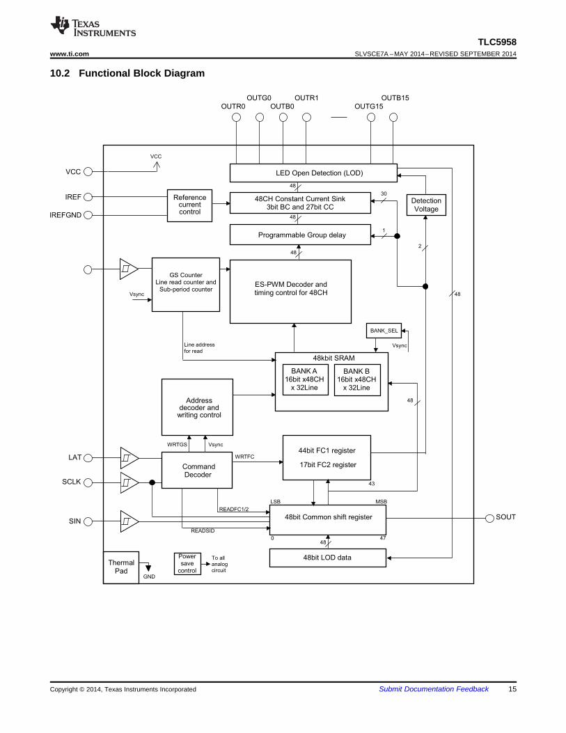
10 Detailed Description
10.1 OverviewThe TLC5958 is a 48 channels constant-current sink driver for multiplexing system with 1 to 32 duty ratio. Eachchannel has an individually-adjustable, 65536-step, pulse width modulation (PWM) grayscale (GS).
48K bit display memory is implemented to increase the visual refresh rate and to decrease the GS data writingfrequency.
The TLC5958 support output current range from 1mA to 25mA, channel-to-channel accuracy is 3% max, device-to-device accuracy is 2% max in all current range. Besides, it implement Low Gray Scale Enhancement(LGSE™) technology to improve the display quality at low grayscale condition. These features make TLC5958more suitable for high-density multiplexing application.
The output channels are grouped into three groups, each group has 16 channels. Each group has a 512-stepcolor brightness control (CC) function. The maximum current value of all 48 channels can be set by 8-step globalbrightness control (BC) function. CC and BC can be used to adjust the brightness deviation between LEDdrivers. GS, CC, and BC data are accessible via a serial interface port.
The TLC5958 has one error flag: LED open detection (LOD), which can be read via a serial interface port.Besides, The TLC5958 also have Thermal shut down(TSD) and Iref resistor short protection(ISP), which makesure a higher system reliability. The TLC5958 also has a power-save mode that sets the total currentconsumption to 0.8mA (typ) when all outputs are off.
14 Submit Documentation Feedback Copyright © 2014, Texas Instruments Incorporated
GS CounterLine read counter and
Sub-period counterES-PWM Decoder andtiming control for 48CH
VCC
SIN48bit Common shift register
48CH Constant Current Sink3bit BC and 27bit CC
OUTR0
VCC
LED Open Detection (LOD)
OUTR1
GND
0
MSBLSB
47
SCLK
LAT
SOUT
OUTG0
OUTG15OUTB0
OUTB15
Powersave
control
To allanalogcircuit
48
2
IREF
IREFGND
ThermalPad
Referencecurrentcontrol
48
Programmable Group delay
DetectionVoltage
48
48
Vsync
48kbit SRAM
BANK A16bit x48CH
x 32Line
BANK B16bit x48CH
x 32Line
Line address
for read
48bit LOD data
CommandDecoder
WRTGS
BANK_SEL
WRTFC
READFC1/2
READSID
48
30
1
48
Vsync
Vsync
Addressdecoder and
writing control
43
44bit FC1 register
17bit FC2 register
TLC5958www.ti.com SLVSCE7A –MAY 2014–REVISED SEPTEMBER 2014
10.2 Functional Block Diagram
Copyright © 2014, Texas Instruments Incorporated Submit Documentation Feedback 15

TLC5958SLVSCE7A –MAY 2014–REVISED SEPTEMBER 2014 www.ti.com
10.3 Device Functional ModesAfter power on, all OUTXn of the TLC5958 are turned off. All the internal counters and function control registers(FC1/FC2) are initialized. The following list is a brief summary of the sequence to operate the TLC5958, to giveusers a general idea how the device works. After that, the function block related to each step is detailed in thefollowing sections.1. According to required LED current, choose BC & CC code, select the current programming resistor RIREF.2. Send WRTFC command to set FC1/2 register value if the default value need be changed.3. Write GS data of all lines (max 32 lines) into one of the two memory BANKs.4. Send Vsync command, the BANK with the GS data written just now will be displayed.5. Input GCLK continuously, 257GCLK (or 513GCLK) as a segment. Between the interval of two segments,
supply voltage should be switched from one line to next line accordingly.6. During the same period of step 5, GS data for next frame should be written into another BANK.7. When the time of one frame ends, Vsync command should be input to swap the purpose of the two BANKs.
Repeat step 5 through 7.
10.3.1 Brightness Control (BC) FunctionThe TLC5958 is able to adjust the output current of all constant-current outputs simultaneously. This function iscalled global brightness control (BC). The global BC for all outputs is programmed with a 3-bit word, thus alloutput currents can be adjusted in 8 steps from 12.9% to 100% for a given current-programming resistor, RIREF(See Table 2).
BC data can be set via the serial interface. When the BC data changes, the output current also changesimmediately. When the device is powered on, the BC data in the function control (FC) register FC1 is set to 4has the initial value.
10.3.2 Color Brightness Control (CC) FunctionThe TLC5958 is able to adjust the output current of each of the three color groups OUTR0-OUTR15, OUTG0-OUTG15, and OUTB0-OUTB15 separately. This function is called color brightness control (CC). For each color,it has 9-bit data latch CCR,CCG, or CCB in FC1 register . Thus, all color group output currents can be adjustedin 512 steps from 0% to 100% of the maximum output current, IOLCMax. (See the next section for more detailabout IOLCMax). The CC data are entered via the serial interface. When the CC data change, the output currentalso changes immediately.
When the IC is powered on, the CC data are set to ‘100h’. Equation 1 calculates the actual output current.Iout(mA) = IOLCMax(mA) × ( CCR/511d or CCG/511d or CCB/511d) (1)
Where:IOLCMax = the maximum channel current for each channel, determined by BC data and RIREF (See Equation 2)CCR/G/B = the color brightness control value for each color group in the FC1 register (000h to 1FFh)
Table 1 shows the CC data versus the constant-current against IOLCMax.
16 Submit Documentation Feedback Copyright © 2014, Texas Instruments Incorporated

TLC5958www.ti.com SLVSCE7A –MAY 2014–REVISED SEPTEMBER 2014
Device Functional Modes (continued)Table 1. CC Data vs Current Ratio and Set Current Value
RATIO OF OUTPUTCC DATA (CCR or CCG or CCB) CURRENT OUTPUT CURRENT (mA, RIREF = 7.41 kΩ)
TO IolcMax(%, typical)BC = 7h BC = 0hBINARY DECIMAL HEX (IolcMax =25mA) (IolcMax=3.2mA)
0 0000 0000 0 00 0 0 00 0000 0001 1 01 0.2 0.05 0.0060 0000 0010 2 02 0.4 0.10 0.013
--- --- --- --- --- ---1 0000 0000 256 100 50.1 12.52 1.621(Default) (Default) (Default)
--- --- --- --- --- ---1 1111 1101 509 1FD 99.6 24.90 3.2221 1111 1110 510 1FE 99.8 24.95 3.2291 1111 1111 511 1FF 100.0 25 3.235
10.3.3 Select RIREF For a Given BCThe maximum output current per channel, IOLCMax, is determined by resistor RIREF, placed between the IREF andIREFGND pins, and the BC code in FC1 register. The voltage on IREF is typically 1.209V. RIREF can becalculated by Equation 2.
Riref(kΩ) = Viref(V) / IOLCMax(mA) × Gain (2)
Where:VIREF = the internal reference voltage on IREF (1.209V, typical)IOLCMax is the largest current for each output at CCR/G/B=1FFh.Gain = the current gain at a selected BC code (See Table 2 )
Table 2. Current Gain Versus BC CodeBC DATA RATIO OF
GAIN GAIN / GAIN_MAX (AT MAXBINARY HEX BC)
000 (recommend) 0 (recommend 20.4 12.9%001 1 40.3 25.6%010 2 59.7 52.4%011 3 82.4 12.9%
100 (default) 4 (default) 101.8 64.7%101 5 115.4 73.3%110 6 144.3 91.7%111 7 157.4 100%
NOTE: Recommend using a smaller BC code for better performance. For noise immunity purposes, suggest RIREF < 60 kΩ
10.3.4 Choosing BC/CC For a Different ApplicationBC is mainly used for global brightness adjustment between day and night. Suggested BC is 4h, which is in themiddle of the range, thus, one can change brightness up and down flexibly.
CC can be used to fine tune the brightness in 512 steps, this is suitable for white balance adjustment betweenRGB color group. To get a pure white color, the general requirement for the luminous intensity ratio of R, G, BLED is 3:6:1. Depending on the characteristics of the LED (Electro-Optical conversion efficiency), the currentratio of R, G, B LED will be much different from this ratio. Usually, the Red LED needs the largest current. Onecan choose 511d (the max value) CC code for the color group that needs the largest initial current, then chooseproper CC code for the other two color groups according to the current ratio requirement of the LED used.
Copyright © 2014, Texas Instruments Incorporated Submit Documentation Feedback 17

TLC5958SLVSCE7A –MAY 2014–REVISED SEPTEMBER 2014 www.ti.com
10.3.4.1 Example 1: Red LED Current is 20mA, Green LED Needs 12mA, Blue LED needs 8mA1. Red LED needs the largest current, so choose 511d for CCR2. 511 x 12mA / 20mA = 306.6, thus choose 307d for CCG. With same method, choose 204d for CCB.3. According to the required red LED current, choose 7h for BC.4. According to Equation 2, RIREF = 1.209V/20mA x 157.4 = 9.5 kΩ
In this example, we choose 7h for BC, instead of using the default 4h. This is because the Red LED current is20mA, approaching the upper limit of current range. To prevent the constant output current from exceeding theupper limit in case a larger BC code is input accidently, we choose the maximum BC code here.
10.3.4.2 Example 2: Red LED Current is 5mA, Green LED Needs 2mA, Blue LED Needs 1mA.1. Red LED needs the largest current, so choose 511d for CCR.2. 511 x 2mA / 5mA = 204.4, thus choose 204d for CCG. With same method, choose 102d for CCB.3. According to the required blue LED current, choose 0h for BC.4. According to Equation 2, RIREF = 1.209V / 5mA x 20.4 = 4.93 kΩ
In this example, we choose 0h for BC, instead of using the default 4h. This is because the Blue LED current is1mA, is approaching the lower limit of current range. To prevent the constant output current from exceeding thelower limit in case a lower BC code is input accidently, we choose the minimum BC code here. In general, if LEDcurrent is in the middle of the range (i.e, 10mA), one can just use the default 4h as BC code.
10.3.5 LED Open Detection (LOD)The LOD function detects faults caused by an open circuit in any LED string; or, a short from OUTXn to groundwith low impedance. It does this by comparing the OUTXn voltage to the LOD detection threshold voltage levelset by LODVLT in the FC1 register. If the OUTXn voltage is lower than the programmed voltage, thecorresponding output LOD bit will be set to '1' to indicate a open LED. Otherwise, the output of that LOD bit is '0'.LOD data output by the detection circuit are valid only during the ‘on’ period of that OUTXn output channel. TheLOD data are always ‘0’ for outputs that are turned off.
10.3.6 Power Save Mode (PSM)The power-save mode (PSM) is enabled by setting PSAVE_ENA (bit5 of FC2 register) to ‘1’. When power on,this bit default is ‘0’.
When this function is enabled, if the GS data received for next frame is all ‘0’, IC will enter power save mode atthe moment Vsync command input.
When the IC is in power-save mode, it resumes normal mode when it detects non-zero GS data input. In power-save mode all analog circuits such as constant current output and the LOD circuit are not operational; the devicetotal current consumption, Icc, is below 1mA.
10.3.7 Internal Pre-Charge FETThe internal pre-charge FET can prevent ghosting of multiplexed LED modules. One cause of this phenomenonis the charging current for parasitic capacitance of the OUTXn through the LED when the supply voltage switchesfrom one common line to the next common line.
To prevent this unwanted charging current, TLC5958 uses an internal FET to pull OUTXn up to VCC –1.4Vduring the common line switching period. Thus, no charging current flows through LED and ghosting iseliminated.
10.3.8 Thermal Shutdown (TSD)The thermal shutdown (TSD) function turns off all IC constant-current outputs when the junction temperature (TJ)exceeds 170°C (typ). It resumes normal operation when TJ falls below 160°C (typ).
18 Submit Documentation Feedback Copyright © 2014, Texas Instruments Incorporated

TLC5958www.ti.com SLVSCE7A –MAY 2014–REVISED SEPTEMBER 2014
10.3.9 IREF Resistor Short Protection (ISP)The Iref resistor short protection (ISP) function prevents unwanted large currents from flowing though theconstant-current output when the Iref resistor is shorted accidently. The TLC5958 turns off all output channelswhen the Iref pin voltage is lower than 0.19V (typ). When the Iref pin voltage goes higher than 0.325V (typ), theTLC5958 resumes normal operation.
10.3.10 Noise ReductionLarge surge currents may flow through the IC and the board on which the device is mounted if all 48 LEDchannels turned on simultaneously at the 1st GCLK rising edge. This large surge current could inducedetrimental noise and electromagnetic interference (EMI) into other circuits.
The TLC5958 separates the LED channels into 12 groups. Each group turns on sequentially with some delaybetween one group and the next group. By this operation, a soft-start feature provides for minimal inrush current.
Copyright © 2014, Texas Instruments Incorporated Submit Documentation Feedback 19
TLC5958SLVSCE7A –MAY 2014–REVISED SEPTEMBER 2014 www.ti.com
11 Application and Implementation
Send request via email for Application Note: Build High Density, High Refresh Rate, Multiplexing LED Panel withTLC5958
12 Power Supply RecommendationsThe VCC power supply voltage should be decoupled by placing a 0.1 µF ceramic capacitor close to VCC pin andGND plane. Depending on panel size, several electrolytic capacitors must be placed on board equally distributedto get a well regulated LED supply voltage (VLED). VLED voltage ripple should be less than 5% of its nominalvalue. Furthermore, the VLED should be set to the voltage calculated by equation:
VLED > Vf + 0.4V (10mA constant current example) (3)
Where: Vf = maximum forward voltage of LED
13 Layout
13.1 Layout Guidelines1. Place the decoupling capacitor near the VCC pin and GND plane.2. Place the current programming resistor Riref close to IREF pin and IREFGND pin.3. Route the GND pattern as widely as possible for large GND currents. Maximum GND current is
approximately 1.2A4. Routing between the LED cathode side and the device OUTXn pin should be as short and straight as
possible to reduce wire inductance.5. The PowerPAD™ must be connected to GND plane because the pad is used as power ground pin internally,
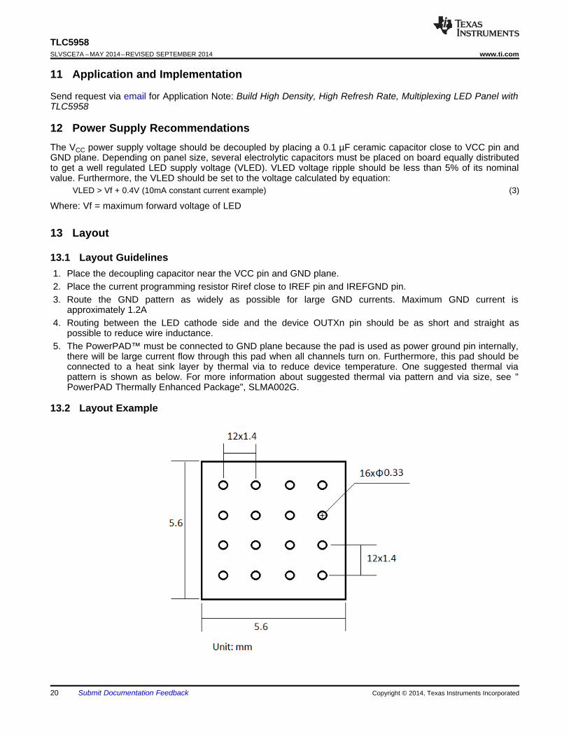
there will be large current flow through this pad when all channels turn on. Furthermore, this pad should beconnected to a heat sink layer by thermal via to reduce device temperature. One suggested thermal viapattern is shown as below. For more information about suggested thermal via pattern and via size, see "PowerPAD Thermally Enhanced Package", SLMA002G.
13.2 Layout Example
20 Submit Documentation Feedback Copyright © 2014, Texas Instruments Incorporated

TLC5958www.ti.com SLVSCE7A –MAY 2014–REVISED SEPTEMBER 2014
14 Device and Documentation Support
14.1 TrademarksLGSE, PowerPAD are trademarks of Texas Instruments.All other trademarks are the property of their respective owners.
14.2 Electrostatic Discharge CautionThese devices have limited built-in ESD protection. The leads should be shorted together or the device placed in conductive foamduring storage or handling to prevent electrostatic damage to the MOS gates.
14.3 GlossarySLYZ022 — TI Glossary.
This glossary lists and explains terms, acronyms, and definitions.
15 Mechanical, Packaging, and Orderable InformationThe following pages include mechanical, packaging, and orderable information. This information is the mostcurrent data available for the designated devices. This data is subject to change without notice and revision ofthis document. For browser-based versions of this data sheet, refer to the left-hand navigation.
Copyright © 2014, Texas Instruments Incorporated Submit Documentation Feedback 21

PACKAGE OPTION ADDENDUM
www.ti.com 10-Dec-2020
Addendum-Page 1
PACKAGING INFORMATION
Orderable Device Status(1)
Package Type PackageDrawing
Pins PackageQty
Eco Plan(2)
Lead finish/Ball material
(6)
MSL Peak Temp(3)
Op Temp (°C) Device Marking(4/5)
Samples
TLC5958RTQR ACTIVE QFN RTQ 56 2000 RoHS & Green NIPDAU Level-3-260C-168 HR -40 to 85 TLC5958
TLC5958RTQT ACTIVE QFN RTQ 56 250 RoHS & Green NIPDAU Level-3-260C-168 HR -40 to 85 TLC5958
(1) The marketing status values are defined as follows:ACTIVE: Product device recommended for new designs.LIFEBUY: TI has announced that the device will be discontinued, and a lifetime-buy period is in effect.NRND: Not recommended for new designs. Device is in production to support existing customers, but TI does not recommend using this part in a new design.PREVIEW: Device has been announced but is not in production. Samples may or may not be available.OBSOLETE: TI has discontinued the production of the device.
(2) RoHS: TI defines "RoHS" to mean semiconductor products that are compliant with the current EU RoHS requirements for all 10 RoHS substances, including the requirement that RoHS substancedo not exceed 0.1% by weight in homogeneous materials. Where designed to be soldered at high temperatures, "RoHS" products are suitable for use in specified lead-free processes. TI mayreference these types of products as "Pb-Free".RoHS Exempt: TI defines "RoHS Exempt" to mean products that contain lead but are compliant with EU RoHS pursuant to a specific EU RoHS exemption.Green: TI defines "Green" to mean the content of Chlorine (Cl) and Bromine (Br) based flame retardants meet JS709B low halogen requirements of <=1000ppm threshold. Antimony trioxide basedflame retardants must also meet the <=1000ppm threshold requirement.
(3) MSL, Peak Temp. - The Moisture Sensitivity Level rating according to the JEDEC industry standard classifications, and peak solder temperature.
(4) There may be additional marking, which relates to the logo, the lot trace code information, or the environmental category on the device.
(5) Multiple Device Markings will be inside parentheses. Only one Device Marking contained in parentheses and separated by a "~" will appear on a device. If a line is indented then it is a continuationof the previous line and the two combined represent the entire Device Marking for that device.
(6) Lead finish/Ball material - Orderable Devices may have multiple material finish options. Finish options are separated by a vertical ruled line. Lead finish/Ball material values may wrap to twolines if the finish value exceeds the maximum column width.
Important Information and Disclaimer:The information provided on this page represents TI's knowledge and belief as of the date that it is provided. TI bases its knowledge and belief on informationprovided by third parties, and makes no representation or warranty as to the accuracy of such information. Efforts are underway to better integrate information from third parties. TI has taken andcontinues to take reasonable steps to provide representative and accurate information but may not have conducted destructive testing or chemical analysis on incoming materials and chemicals.TI and TI suppliers consider certain information to be proprietary, and thus CAS numbers and other limited information may not be available for release.
In no event shall TI's liability arising out of such information exceed the total purchase price of the TI part(s) at issue in this document sold by TI to Customer on an annual basis.

PACKAGE OPTION ADDENDUM
www.ti.com 10-Dec-2020
Addendum-Page 2

TAPE AND REEL INFORMATION
*All dimensions are nominal
Device PackageType
PackageDrawing
Pins SPQ ReelDiameter
(mm)
ReelWidth
W1 (mm)
A0(mm)
B0(mm)
K0(mm)
P1(mm)
W(mm)
Pin1Quadrant
TLC5958RTQR QFN RTQ 56 2000 330.0 16.4 8.3 8.3 1.1 12.0 16.0 Q2
TLC5958RTQT QFN RTQ 56 250 180.0 16.4 8.3 8.3 1.1 12.0 16.0 Q2
PACKAGE MATERIALS INFORMATION
www.ti.com 23-Jun-2015
Pack Materials-Page 1
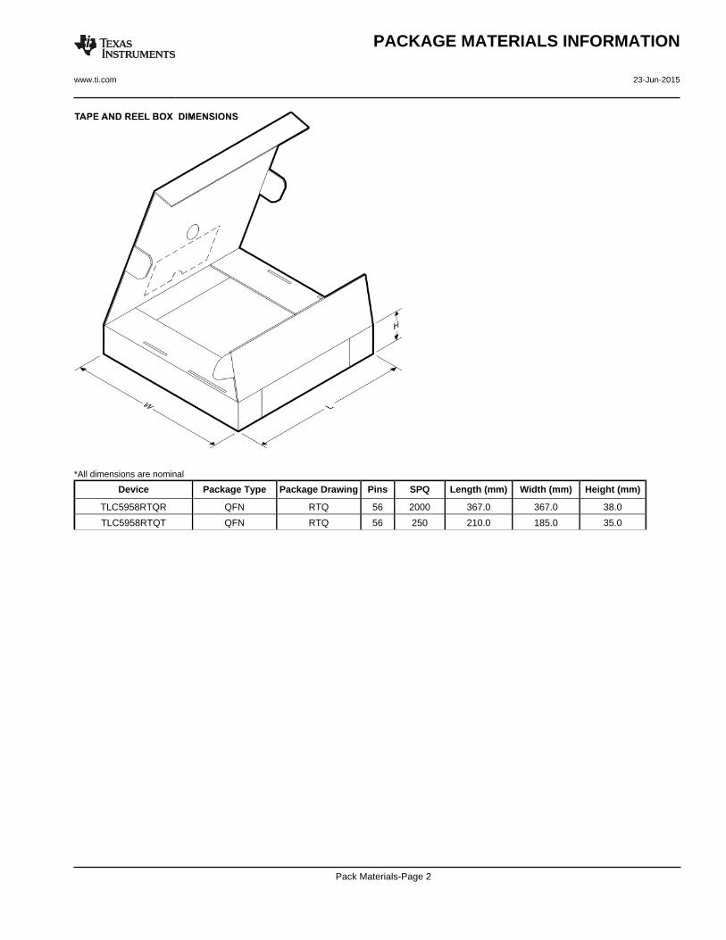
*All dimensions are nominal
Device Package Type Package Drawing Pins SPQ Length (mm) Width (mm) Height (mm)
TLC5958RTQR QFN RTQ 56 2000 367.0 367.0 38.0
TLC5958RTQT QFN RTQ 56 250 210.0 185.0 35.0
PACKAGE MATERIALS INFORMATION
www.ti.com 23-Jun-2015
Pack Materials-Page 2

www.ti.com
GENERIC PACKAGE VIEW
Images above are just a representation of the package family, actual package may vary.Refer to the product data sheet for package details.
VQFN - 1 mm max heightRTQ 56PLASTIC QUAD FLATPACK - NO LEAD8 x 8, 0.5 mm pitch
4224653/A
NOTES:
1. All linear dimensions are in millimeters. Any dimensions in parenthesis are for reference only. Dimensioning and tolerancingper ASME Y14.5M.
2. This drawing is subject to change without notice.3. The package thermal pad must be soldered to the printed circuit board for thermal and mechanical performance.
PACKAGE OUTLINE
www.ti.com
4225369 / A 10/2019
VQFN - 1 mm max height
PLASTIC QUAD FLATPACK-NO LEAD
RTQ0056G
A
0.08 C
0.1 C A B0.05 C
B
SYMM
SYMM
8.157.85
8.157.85
1 MAX
0.050.00
SEATING PLANE
PIN 1 INDEX AREA
C
5.6±0.1
5.6±0.14X6.5
PIN 1 ID(OPTIONAL)
1
14
15 28
29
42
4356
52X 0.5
56X 0.50.3
56X 0.300.18
(0.2) TYP
57
AutoCAD SHX Text
AutoCAD SHX Text

NOTES: (continued)
4. This package is designed to be soldered to a thermal pad on the board. For more information, see Texas Instrumentsliterature number SLUA271 (www.ti.com/lit/slua271).
5. Vias are optional depending on application, refer to device data sheet. If any vias are implemented, refer to theirlocations shown on this view. it is recommended thar vias under paste be filled, plugged or tented.
EXAMPLE BOARD LAYOUT
4225369 / A 10/2019
www.ti.com
VQFN - 1 mm max height
RTQ0056G
PLASTIC QUAD FLATPACK-NO LEAD
SYMM
SYMM
LAND PATTERN EXAMPLESCALE: 10X
(7.8)
1
14
15 28
29
42
4356
(0.78)
56X (0.24)
56X (0.6)
52X (0.5)
(R0.05)TYP
0.07 MAXALL AROUND 0.07 MIN
ALL AROUND
METAL
SOLDER MASKOPENING
SOLDER MASKOPENING
METAL UNDERSOLDER MASK
SOLDER MASK DETAILS
NON SOLDER MASKDEFINED
(PREFERRED)SOLDER MASK
DEFINED
57
(5.6)
(5.6)
(Ø0.2) TYPVIA
8X (1.33) 6X (1.22)
8X (1.33)
6X (1.22)
AutoCAD SHX Text
AutoCAD SHX Text

NOTES: (continued)
6. Laser cutting apertures with trapezoidal walls and rounded corners may offer better paste release. IPC-7525 may have alternatedesign recommendations..
EXAMPLE STENCIL DESIGN
4225369 / A 10/2019
www.ti.com
VQFN - 1 mm max height
RTQ0056G
PLASTIC QUAD FLATPACK-NO LEAD
SYMM
SYMM
SOLDER PASTE EXAMPLEBASED ON 0.125 mm THICK STENCIL
EXPOSED PAD66% PRINTED COVERAGE BY AREA
SCALE: 10X
1
14
15 28
29
42
4356
(7.8)
(7.8)
METALTYP
57
56X (0.24)
56X (0.6)
(R0.05) TYP
8X (0.665)
16X( 1.13)
52X (0.5)
8X (1.33)
8X (0.665)
8X (1.33)
AutoCAD SHX Text
AutoCAD SHX Text

IMPORTANT NOTICE AND DISCLAIMER
TI PROVIDES TECHNICAL AND RELIABILITY DATA (INCLUDING DATASHEETS), DESIGN RESOURCES (INCLUDING REFERENCE DESIGNS), APPLICATION OR OTHER DESIGN ADVICE, WEB TOOLS, SAFETY INFORMATION, AND OTHER RESOURCES “AS IS” AND WITH ALL FAULTS, AND DISCLAIMS ALL WARRANTIES, EXPRESS AND IMPLIED, INCLUDING WITHOUT LIMITATION ANY IMPLIED WARRANTIES OF MERCHANTABILITY, FITNESS FOR A PARTICULAR PURPOSE OR NON-INFRINGEMENT OF THIRD PARTY INTELLECTUAL PROPERTY RIGHTS.These resources are intended for skilled developers designing with TI products. You are solely responsible for (1) selecting the appropriate TI products for your application, (2) designing, validating and testing your application, and (3) ensuring your application meets applicable standards, and any other safety, security, or other requirements. These resources are subject to change without notice. TI grants you permission to use these resources only for development of an application that uses the TI products described in the resource. Other reproduction and display of these resources is prohibited. No license is granted to any other TI intellectual property right or to any third party intellectual property right. TI disclaims responsibility for, and you will fully indemnify TI and its representatives against, any claims, damages, costs, losses, and liabilities arising out of your use of these resources.TI’s products are provided subject to TI’s Terms of Sale (www.ti.com/legal/termsofsale.html) or other applicable terms available either on ti.com or provided in conjunction with such TI products. TI’s provision of these resources does not expand or otherwise alter TI’s applicable warranties or warranty disclaimers for TI products.
Mailing Address: Texas Instruments, Post Office Box 655303, Dallas, Texas 75265Copyright © 2020, Texas Instruments Incorporated