TLC591x 8-Channel Constant-Current LED Sink Drivers · • Automotive LED Lighting the end of the...
40
. . . VLED GND SDO R-EXT VDD LE CLK SDI LE CLK OE OE SDI Controller OUT0 . . . 3.0V to 5.5V OUT1 OUT6 OUT7 TLC5917 To Controller if Error Detection Used Product Folder Sample & Buy Technical Documents Tools & Software Support & Community TLC5916, TLC5917 SLVS695D – JUNE 2007 – REVISED JANUARY 2015 TLC591x 8-Channel Constant-Current LED Sink Drivers 1 Features 3 Description The TLC591x Constant-Current LED Sink Drivers are 1• Eight Constant-Current Output Channels designed to work alone or cascaded. Since each • Output Current Adjusted Through Single External output is independently controlled, they can be Resistor programmed to be on or off by the user. The high • Constant Output Current Range: 3-mA to 120-mA LED voltage (VLED) allows for the use of a single LED per output or multiple LEDs on a single string. per Channel With independently controlled outputs supplied with • Constant Output Current Invariant to Load Voltage constant current, the LEDs can be combined in Change parallel to create higher currents on a single string. • Open Load, Short Load and Overtemperature The constant sink current for all channels is set Detection through a single external resistor. This allows different LED drivers in the same application to sink • 256-Step Programmable Global Current Gain various currents which provides optional • Excellent Output Current Accuracy: implementation of multi-color LEDs. An additional – Between Channels: < ±3% (Maximum) advantage of the independent outputs is the ability to – Between ICs: < ±6% (Maximum) leave unused channels floating. The flexibility of the TLC591x LED drivers is ideal for applications such as • Fast Response of Output Current (but not limited to): 7-segment displays, scrolling • 30-MHz Clock Frequency single color displays, gaming machines, white goods, • Schmitt-Trigger Input video billboards and video panels. • 3.3-V or 5-V Supply Voltage Device Information (1) • Maximum LED Voltage 20-V PART NUMBER PACKAGE BODY SIZE (NOM) • Thermal Shutdown for Overtemperature SOIC (16) 9.90 mm × 3.91 mm Protection TLC5916 PDIP (16) 19.30 mm × 6.35 mm TSSOP (16) 5.00 mm × 4.40 mm 2 Applications SOIC (16) 9.90 mm × 3.91 mm • General LED Lighting Applications TLC5917 PDIP (16) 19.30 mm × 6.35 mm • LED Display Systems TSSOP (16) 5.00 mm × 4.40 mm • LED Signage (1) For all available packages, see the orderable addendum at • Automotive LED Lighting the end of the datasheet. • White Goods • Gaming Machines/Entertainment Single Implementation of TLC5916 / TLC5917 Device 1 An IMPORTANT NOTICE at the end of this data sheet addresses availability, warranty, changes, use in safety-critical applications, intellectual property matters and other important disclaimers. PRODUCTION DATA.
Transcript of TLC591x 8-Channel Constant-Current LED Sink Drivers · • Automotive LED Lighting the end of the...

. . .
VLED
GND
SDO
R-EXT
VDD
LE
CLK
SDI
LE
CLK
OE OE
SDI
Co
ntr
olle
r
OU
T0
. . .
3.0V to 5.5V
OU
T1
OU
T6
OU
T7
TLC5917To Controller if Error
Detection Used
Product
Folder
Sample &Buy
Technical
Documents
Tools &
Software
Support &Community
TLC5916, TLC5917SLVS695D –JUNE 2007–REVISED JANUARY 2015
TLC591x 8-Channel Constant-Current LED Sink Drivers1 Features 3 Description
The TLC591x Constant-Current LED Sink Drivers are1• Eight Constant-Current Output Channels
designed to work alone or cascaded. Since each• Output Current Adjusted Through Single External output is independently controlled, they can beResistor programmed to be on or off by the user. The high
• Constant Output Current Range: 3-mA to 120-mA LED voltage (VLED) allows for the use of a singleLED per output or multiple LEDs on a single string.per ChannelWith independently controlled outputs supplied with• Constant Output Current Invariant to Load Voltageconstant current, the LEDs can be combined inChange parallel to create higher currents on a single string.
• Open Load, Short Load and Overtemperature The constant sink current for all channels is setDetection through a single external resistor. This allows
different LED drivers in the same application to sink• 256-Step Programmable Global Current Gainvarious currents which provides optional• Excellent Output Current Accuracy:implementation of multi-color LEDs. An additional
– Between Channels: < ±3% (Maximum) advantage of the independent outputs is the ability to– Between ICs: < ±6% (Maximum) leave unused channels floating. The flexibility of the
TLC591x LED drivers is ideal for applications such as• Fast Response of Output Current(but not limited to): 7-segment displays, scrolling• 30-MHz Clock Frequency single color displays, gaming machines, white goods,
• Schmitt-Trigger Input video billboards and video panels.• 3.3-V or 5-V Supply Voltage
Device Information(1)• Maximum LED Voltage 20-V
PART NUMBER PACKAGE BODY SIZE (NOM)• Thermal Shutdown for OvertemperatureSOIC (16) 9.90 mm × 3.91 mmProtection
TLC5916 PDIP (16) 19.30 mm × 6.35 mmTSSOP (16) 5.00 mm × 4.40 mm2 ApplicationsSOIC (16) 9.90 mm × 3.91 mm• General LED Lighting Applications
TLC5917 PDIP (16) 19.30 mm × 6.35 mm• LED Display SystemsTSSOP (16) 5.00 mm × 4.40 mm
• LED Signage(1) For all available packages, see the orderable addendum at• Automotive LED Lighting the end of the datasheet.
• White Goods• Gaming Machines/Entertainment
Single Implementation of TLC5916 / TLC5917 Device
1
An IMPORTANT NOTICE at the end of this data sheet addresses availability, warranty, changes, use in safety-critical applications,intellectual property matters and other important disclaimers. PRODUCTION DATA.

TLC5916, TLC5917SLVS695D –JUNE 2007–REVISED JANUARY 2015 www.ti.com
Table of Contents1 Features .................................................................. 1 9 Detailed Description ............................................ 13
9.1 Overview ................................................................. 132 Applications ........................................................... 19.2 Functional Block Diagram ....................................... 143 Description ............................................................. 19.3 Feature Description................................................. 144 Revision History..................................................... 29.4 Device Functional Modes........................................ 165 Device Comparison Table ..................................... 3
10 Application and Implementation........................ 216 Pin Configuration and Functions ......................... 310.1 Application Information.......................................... 217 Specifications......................................................... 410.2 Typical Application ................................................ 247.1 Absolute Maximum Ratings ...................................... 4
11 Power Supply Recommendations ..................... 277.2 ESD Ratings.............................................................. 412 Layout................................................................... 277.3 Recommended Operating Conditions....................... 4
12.1 Layout Guidelines ................................................. 277.4 Thermal Information .................................................. 412.2 Layout Example .................................................... 277.5 Electrical Characteristics: VDD = 3 V......................... 5
13 Device and Documentation Support ................. 297.6 Electrical Characteristics: VDD = 5.5 V...................... 613.1 Related Links ........................................................ 297.7 Switching Characteristics: VDD = 3 V........................ 713.2 Trademarks ........................................................... 297.8 Switching Characteristics: VDD = 5.5 V..................... 813.3 Electrostatic Discharge Caution............................ 297.9 Timing Requirements ................................................ 913.4 Glossary ................................................................ 297.10 Typical Characteristics ............................................ 9
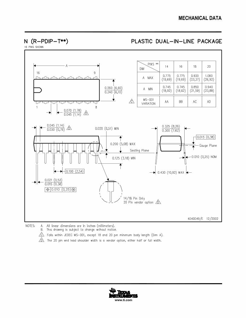
14 Mechanical, Packaging, and Orderable8 Parameter Measurement Information ................ 10Information ........................................................... 29
4 Revision HistoryNOTE: Page numbers for previous revisions may differ from page numbers in the current version.
Changes from Revision C (February 2011) to Revision D Page
• Added Pin Configuration and Functions section, ESD Ratings table, Feature Description section, Device FunctionalModes, Application and Implementation section, Power Supply Recommendations section, Layout section, Deviceand Documentation Support section, and Mechanical, Packaging, and Orderable Information section .............................. 1
Changes from Revision B (February 2011) to Revision C Page
• Replaced the Power Dissipation and Thermal Impedance table with the Thermal Information tables.................................. 4
Changes from Revision A (November 2010) to Revision B Page
• Added Maximum LED Voltage 20-V to Features. .................................................................................................................. 1• Added Abstract section........................................................................................................................................................... 1• Changed resistor value in Single Implementation diagram from 840Ω to 720Ω. ................................................................. 13• Changed Default Relationship Curve to reflect correct data. .............................................................................................. 21• Changed resistor value in Cascading Implementation diagram from 840Ω to 720Ω. .......................................................... 22• Changed resistor value in Single Implementation diagram from 840Ω to 720Ω. ................................................................. 24
2 Submit Documentation Feedback Copyright © 2007–2015, Texas Instruments Incorporated
Product Folder Links: TLC5916 TLC5917

1
2
3
4
5
6
7
8
16
15
14
13
12
11
10
9
GND
SDI
CLK
LE(ED1)
OUT0
OUT1
OUT2
OUT3
VDD
R-EXT
SDO
OE(ED2)
OUT7
OUT6
OUT5
OUT4
D, N, OR PW PACKAGE
(TOP VIEW)
TLC5916, TLC5917www.ti.com SLVS695D –JUNE 2007–REVISED JANUARY 2015
5 Device Comparison Table
OVERTEMPERATURE OPEN-LOAD SHORT TO GND SHORT TO VLEDDEVICE (1)DETECTION DETECTION DETECTION DETECTION
TLC5916 X X X —TLC5917 X X X X
(1) The device has one single error register for all these conditions (one error bit per channel).
6 Pin Configuration and Functions
16-PIN
Pin FunctionsPIN
I/O DESCRIPTIONNAME NO.CLK 3 I Clock input for data shift on rising edgeGND 1 – Ground for control logic and current sink
Data strobe inputSerial data is transferred to the respective latch when LE(ED1) is high. The data is latchedLE(ED1) 4 I when LE(ED1) goes low. Also, a control signal input for an Error Detection Mode and CurrentAdjust Mode (see Timing Diagram). LE(ED1) has an internal pulldown.Output enable. When OE(ED2) is active (low), the output drivers are enabled; whenOE(ED2) is high, all output drivers are turned OFF (blanked). Also, a control signal input forOE(ED2) 13 I an Error Detection Mode and Current Adjust Mode (see Figure 11). OE(ED2) has an internalpullup.
OUT0 to OUT7 5 to 12 O Constant-current outputsR-EXT 15 I External Resistor - Connect an external resistor to ground to set the current for all outputsSDI 2 I Serial-data input to the Shift registerSDO 14 O Serial-data output to the following SDI of next driver IC or to the microcontrollerVDD 16 I Supply voltage
Copyright © 2007–2015, Texas Instruments Incorporated Submit Documentation Feedback 3
Product Folder Links: TLC5916 TLC5917
TLC5916, TLC5917SLVS695D –JUNE 2007–REVISED JANUARY 2015 www.ti.com
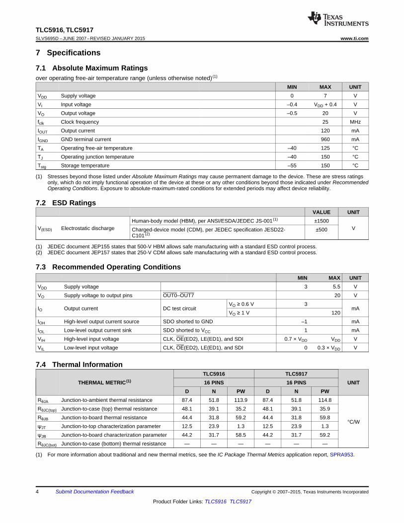
7 Specifications
7.1 Absolute Maximum Ratingsover operating free-air temperature range (unless otherwise noted) (1)
MIN MAX UNITVDD Supply voltage 0 7 VVI Input voltage –0.4 VDD + 0.4 VVO Output voltage –0.5 20 Vfclk Clock frequency 25 MHzIOUT Output current 120 mAIGND GND terminal current 960 mATA Operating free-air temperature –40 125 °CTJ Operating junction temperature –40 150 °CTstg Storage temperature –55 150 °C
(1) Stresses beyond those listed under Absolute Maximum Ratings may cause permanent damage to the device. These are stress ratingsonly, which do not imply functional operation of the device at these or any other conditions beyond those indicated under RecommendedOperating Conditions. Exposure to absolute-maximum-rated conditions for extended periods may affect device reliability.
7.2 ESD RatingsVALUE UNIT
Human-body model (HBM), per ANSI/ESDA/JEDEC JS-001 (1) ±1500V(ESD) Electrostatic discharge VCharged-device model (CDM), per JEDEC specification JESD22- ±500
C101 (2)
(1) JEDEC document JEP155 states that 500-V HBM allows safe manufacturing with a standard ESD control process.(2) JEDEC document JEP157 states that 250-V CDM allows safe manufacturing with a standard ESD control process.
7.3 Recommended Operating ConditionsMIN MAX UNIT
VDD Supply voltage 3 5.5 VVO Supply voltage to output pins OUT0–OUT7 20 V
VO ≥ 0.6 V 3IO Output current DC test circuit mA
VO ≥ 1 V 120IOH High-level output current source SDO shorted to GND –1 mAIOL Low-level output current sink SDO shorted to VCC 1 mAVIH High-level input voltage CLK, OE(ED2), LE(ED1), and SDI 0.7 × VDD VDD VVIL Low-level input voltage CLK, OE(ED2), LE(ED1), and SDI 0 0.3 × VDD V
7.4 Thermal InformationTLC5916 TLC5917
THERMAL METRIC (1) 16 PINS 16 PINS UNITD N PW D N PW
RθJA Junction-to-ambient thermal resistance 87.4 51.8 113.9 87.4 51.8 114.8RθJC(top) Junction-to-case (top) thermal resistance 48.1 39.1 35.2 48.1 39.1 35.9RθJB Junction-to-board thermal resistance 44.4 31.8 59.2 44.4 31.8 59.8
°C/WψJT Junction-to-top characterization parameter 12.5 23.9 1.3 12.5 23.9 1.3ψJB Junction-to-board characterization parameter 44.2 31.7 58.5 44.2 31.7 59.2RθJC(bot) Junction-to-case (bottom) thermal resistance — — — — — —
(1) For more information about traditional and new thermal metrics, see the IC Package Thermal Metrics application report, SPRA953.
4 Submit Documentation Feedback Copyright © 2007–2015, Texas Instruments Incorporated
Product Folder Links: TLC5916 TLC5917

TLC5916, TLC5917www.ti.com SLVS695D –JUNE 2007–REVISED JANUARY 2015
7.5 Electrical Characteristics: VDD = 3 VVDD = 3 V, TJ = –40°C to 125°C (unless otherwise noted)
PARAMETER TEST CONDITIONS MIN TYP (1) MAX UNITVDD Input voltage 3 5.5 VVO Supply voltage to the output pins 20 V
VO ≥ 0.6 V 3IO Output current mA
VO ≥ 1 V 120IOH High-level output current, source –1 mAIOL Low-level output current, sink 1 mAVIH High-level input voltage 0.7 × VDD VDD VVIL Low-level input voltage GND 0.3 × VDD V
TJ = 25°C 0.5Ileak Output leakage current VOH = 17 V μA
TJ = 125°C 2VOH High-level output voltage SDO, IOL = –1 mA VDD – 0.4 VVOL Low-level output voltage SDO, IOH = 1 mA 0.4 V
VOUT = 0.6 V, Rext = 720 Ω,Output current 1 26 mACG = 0.992IOL = 26 mA, VO = 0.6 V, Rext = 720 Ω,IO(1) Output current error, die-die ±3% ±6%TJ = 25°C
Output current skew, channel-to- IOL = 26 mA, VO = 0.6 V, Rext = 720 Ω, ±1.5% ±3%channel TJ = 25°COutput current 2 VO = 0.8 V, Rext = 360 Ω, CG = 0.992 52 mA
IOL = 52 mA, VO = 0.8 V, Rext = 360 Ω,Output current error, die-die ±2% ±6%IO(2) TJ = 25°COutput current skew, channel-to- IOL = 52 mA, VO = 0.8 V, Rext = 360 Ω, ±1.5% ±3%channel TJ = 25°C
VO = 1 V to 3 V, IO = 26 mA ±0.1IOUT vs Output current vs %/VVDD = 3.0 V to 5.5 V,VOUT output voltage regulation ±1IO = 26 mA/120 mA
Pullup resistance OE(ED2) 500 kΩPulldown resistance LE(ED1) 500 kΩ
Tsd Overtemperature shutdown (2) 150 175 200 °CThys Restart temperature hysteresis (2) 15 °C
Threshold current for open error 0.5 ×IOUT,Th IOUT,target = 3 mA to 120 mAdetection Itarget %Trigger threshold voltage for
VOUT,TTh short-error detection IOUT,target = 3 mA to 120 mA 2.5 2.7 3.1 V(TLC5917 only)Return threshold voltage for
VOUT, RTh short-error detection IOUT,target = 3 mA to 120 mA 2.2 V(TLC5917 only)
Rext = Open 5 10Rext = 720 Ω 8 14
IDD Supply current mARext = 360 Ω 11 18Rext = 180 Ω 16 22
(1) Typical values represent the likely parametric nominal values determined at the time of characterization. Typical values depend on theapplication and configuration and may vary over time. Typical values are not ensured on production material.
(2) Specified by design.
Copyright © 2007–2015, Texas Instruments Incorporated Submit Documentation Feedback 5
Product Folder Links: TLC5916 TLC5917
TLC5916, TLC5917SLVS695D –JUNE 2007–REVISED JANUARY 2015 www.ti.com
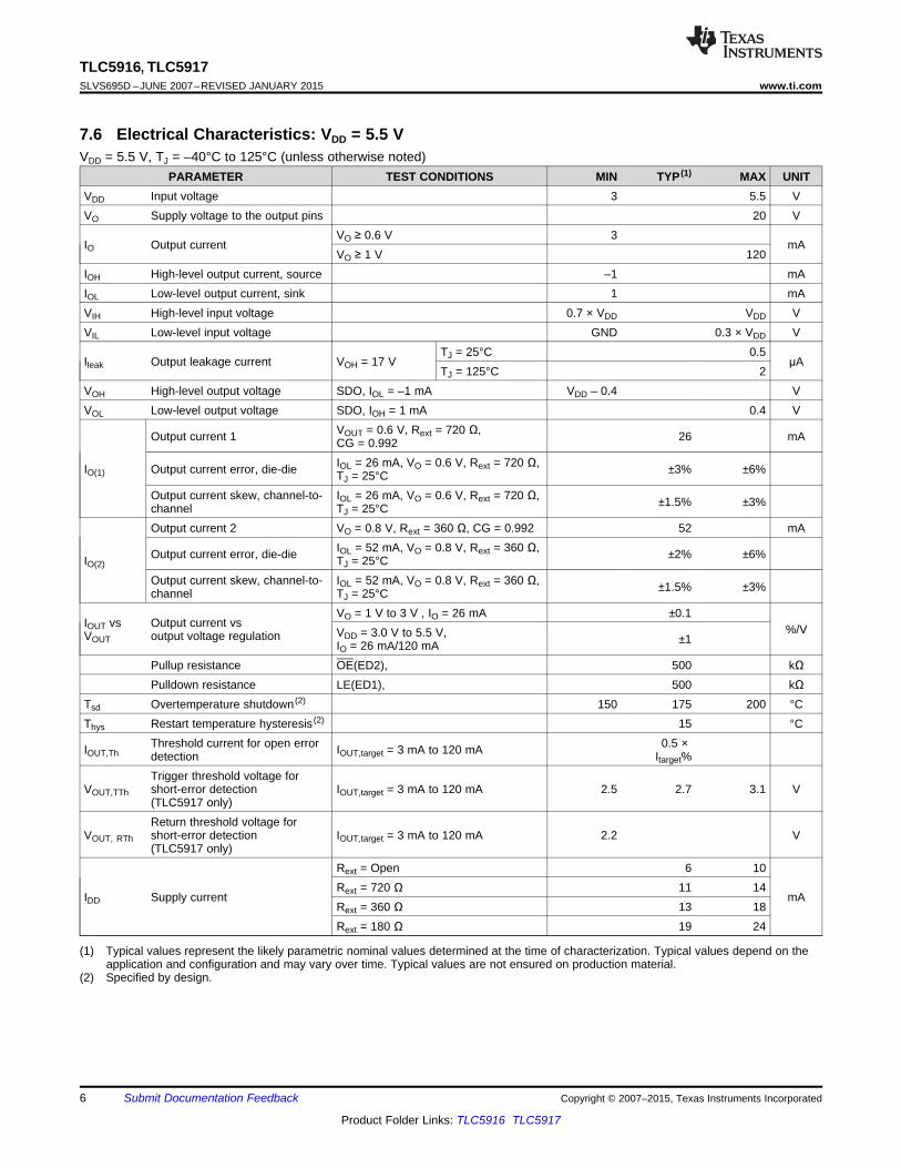
7.6 Electrical Characteristics: VDD = 5.5 VVDD = 5.5 V, TJ = –40°C to 125°C (unless otherwise noted)
PARAMETER TEST CONDITIONS MIN TYP (1) MAX UNITVDD Input voltage 3 5.5 VVO Supply voltage to the output pins 20 V
VO ≥ 0.6 V 3IO Output current mA
VO ≥ 1 V 120IOH High-level output current, source –1 mAIOL Low-level output current, sink 1 mAVIH High-level input voltage 0.7 × VDD VDD VVIL Low-level input voltage GND 0.3 × VDD V
TJ = 25°C 0.5Ileak Output leakage current VOH = 17 V μA
TJ = 125°C 2VOH High-level output voltage SDO, IOL = –1 mA VDD – 0.4 VVOL Low-level output voltage SDO, IOH = 1 mA 0.4 V
VOUT = 0.6 V, Rext = 720 Ω,Output current 1 26 mACG = 0.992IOL = 26 mA, VO = 0.6 V, Rext = 720 Ω,IO(1) Output current error, die-die ±3% ±6%TJ = 25°C
Output current skew, channel-to- IOL = 26 mA, VO = 0.6 V, Rext = 720 Ω, ±1.5% ±3%channel TJ = 25°COutput current 2 VO = 0.8 V, Rext = 360 Ω, CG = 0.992 52 mA
IOL = 52 mA, VO = 0.8 V, Rext = 360 Ω,Output current error, die-die ±2% ±6%IO(2) TJ = 25°COutput current skew, channel-to- IOL = 52 mA, VO = 0.8 V, Rext = 360 Ω, ±1.5% ±3%channel TJ = 25°C
VO = 1 V to 3 V , IO = 26 mA ±0.1IOUT vs Output current vs %/VVDD = 3.0 V to 5.5 V,VOUT output voltage regulation ±1IO = 26 mA/120 mA
Pullup resistance OE(ED2), 500 kΩPulldown resistance LE(ED1), 500 kΩ
Tsd Overtemperature shutdown (2) 150 175 200 °CThys Restart temperature hysteresis (2) 15 °C
Threshold current for open error 0.5 ×IOUT,Th IOUT,target = 3 mA to 120 mAdetection Itarget%Trigger threshold voltage for
VOUT,TTh short-error detection IOUT,target = 3 mA to 120 mA 2.5 2.7 3.1 V(TLC5917 only)Return threshold voltage for
VOUT, RTh short-error detection IOUT,target = 3 mA to 120 mA 2.2 V(TLC5917 only)
Rext = Open 6 10Rext = 720 Ω 11 14
IDD Supply current mARext = 360 Ω 13 18Rext = 180 Ω 19 24
(1) Typical values represent the likely parametric nominal values determined at the time of characterization. Typical values depend on theapplication and configuration and may vary over time. Typical values are not ensured on production material.
(2) Specified by design.
6 Submit Documentation Feedback Copyright © 2007–2015, Texas Instruments Incorporated
Product Folder Links: TLC5916 TLC5917

TLC5916, TLC5917www.ti.com SLVS695D –JUNE 2007–REVISED JANUARY 2015
7.7 Switching Characteristics: VDD = 3 VVDD = 3 V, TJ = –40°C to 125°C (unless otherwise noted)
PARAMETER TEST CONDITIONS MIN TYP (1) MAX UNITtPLH1 Low-to-high propagation delay time, CLK to OUTn 40 65 95 nstPLH2 Low-to-high propagation delay time, LE(ED1) to OUTn 40 65 95 nstPLH3 Low-to-high propagation delay time, OE(ED2) to OUTn 40 65 95 nstPLH4 Low-to-high propagation delay time, CLK to SDO 12 20 30 nstPHL1 High-to-low propagation delay time, CLK to OUTn 300 365 nstPHL2 High-to-low propagation delay time, LE(ED1) to OUTn 300 365 nstPHL3 High-to-low propagation delay time, OE(ED2) to OUTn 300 365 nstPHL4 High-to-low propagation delay time, CLK to SDO 12 20 30 nstw(CLK) Pulse duration, CLK 20 nstw(L) Pulse duration, LE(ED1) 20 nstw(OE) Pulse duration, OE(ED2) 500 ns
VIH = VDD, VIL = GND,tw(ED2) Pulse duration, OE(ED2) in Error Detection Mode 2 μsRext = 360 Ω, VL = 4 V,
RL = 44 Ω, CL = 10 pF,th(ED1,ED2) Hold time, LE(ED1) and OE(ED2) 10 nsCG = 0.992
th(D) Hold time, SDI 2 nstsu(D,ED1) Setup time, SDI, LE(ED1) 3 nstsu(ED2) Setup time, OE(ED2) 8.5 nsth(L) Hold time, LE(ED1), Normal Mode 15 nstsu(L) Setup time, LE(ED1), Normal Mode 15 nstr Rise time, CLK (2) 500 nstf Fall time, CLK (2) 500 nstor Rise time, outputs (off) 40 85 105 nstor Rise time, outputs (off), TJ = 25°C 83 100 nstof Rise time, outputs (on) 100 280 370 nstof Rise time, outputs (on), TJ = 25°C 170 225 nsfCLK Clock frequency Cascade operation 30 MHz
(1) Typical values represent the likely parametric nominal values determined at the time of characterization. Typical values depend on theapplication and configuration and may vary over time. Typical values are not ensured on production material.
(2) If the devices are connected in cascade and tr or tf is large, it may be critical to achieve the timing required for data transfer between twocascaded devices.
Copyright © 2007–2015, Texas Instruments Incorporated Submit Documentation Feedback 7
Product Folder Links: TLC5916 TLC5917

TLC5916, TLC5917SLVS695D –JUNE 2007–REVISED JANUARY 2015 www.ti.com
7.8 Switching Characteristics: VDD = 5.5 VVDD = 5.5 V, TJ = –40°C to 125°C (unless otherwise noted)
PARAMETER TEST CONDITIONS MIN TYP (1) MAX UNITtPLH1 Low-to-high propagation delay time, CLK to OUTn 40 65 95 nstPLH2 Low-to-high propagation delay time, LE(ED1) to OUTn 40 65 95 nstPLH3 Low-to-high propagation delay time, OE(ED2) to OUTn 40 65 95 nstPLH4 Low-to-high propagation delay time, CLK to SDO 8 20 30 nstPHL1 High-to-low propagation delay time, CLK to OUTn 300 365 nstPHL2 High-to-low propagation delay time, LE(ED1) to OUTn 300 365 nstPHL3 High-to-low propagation delay time, OE(ED2) to OUTn 300 365 nstPHL4 High-to-low propagation delay time, CLK to SDO 8 20 30 nstw(CLK) Pulse duration, CLK 20 nstw(L) Pulse duration, LE(ED1) 20 nstw(OE) Pulse duration, OE(ED2) 500 ns
VIH = VDD, VIL = GND,tw(ED2) Pulse duration, OE(ED2) in Error Detection Mode 2 μsRext = 360 Ω, VL = 4 V,
RL = 44 Ω, CL = 10 pF,th(D,ED1,ED2) Hold time, SDI, LE(ED1), and OE(ED2) 10 nsCG = 0.992
th(D) Hold time, SDI 2 nstsu(D,ED1) Setup time, SDI, LE(ED1) 3 nstsu(ED2) Setup time, OE(ED2) 8.5 nsth(L) Hold time, LE(ED1), Normal Mode 15 nstsu(L) Setup time, LE(ED1), Normal Mode 15 nstr Rise time, CLK (2) 500 nstf Fall time, CLK (2) 500 nstor Rise time, outputs (off) 40 85 105 nstor Rise time, outputs (off), TJ = 25°C 83 100 nstof Rise time, outputs (on) 100 280 370 nstof Rise time, outputs (on), TJ = 25°C 170 225 nsfCLK Clock frequency Cascade operation 30 MHz
(1) Typical values represent the likely parametric nominal values determined at the time of characterization. Typical values depend on theapplication and configuration and may vary over time. Typical values are not ensured on production material.
(2) If the devices are connected in cascade and tr or tf is large, it may be critical to achieve the timing required for data transfer between twocascaded devices.
8 Submit Documentation Feedback Copyright © 2007–2015, Texas Instruments Incorporated
Product Folder Links: TLC5916 TLC5917

OE
OUT7
Turn on only one channel
Channel 8
0
25
50
75
100
125
150
0 0.5 1 1.5 2 2.5 3
Output Voltage (V)
Ou
tpu
tC
urr
en
t(m
A)
Temperature = 25°C
IO = 80 mA
IO = 40 mA
IO = 20 mA
IO = 60 mA
IO = 5 mA
IO = 100 mA
IO = 120 mA
OE
OUT1
Turn on only one channel
Channel 1LE = 5 V (active)
= GND (active)OE
CLK
OUTn
TLC5916, TLC5917www.ti.com SLVS695D –JUNE 2007–REVISED JANUARY 2015
7.9 Timing RequirementsVDD = 3 V to 5.5 V (unless otherwise noted)
MIN MAX UNITtw(L) LE(ED1) pulse duration Normal Mode 20 nstw(CLK) CLK pulse duration Normal Mode 20 ns
Normal Mode, IOUT < 60 mA 500tw(OE) OE(ED2) pulse duration ns
Normal Mode, IOUT > 60 mA 700tsu(D) Setup time for SDI Normal Mode 3 nsth(D) Hold time for SDI Normal Mode 2 nstsu(L) Setup time for LE(ED1) Normal Mode 15 nsth(L) Hold time for LE(ED1) Normal Mode 15 nstw(CLK) CLK pulse duration Error Detection Mode 20 nstw(ED2) OE(ED2) pulse duration Error Detection Mode 2000 nstsu(ED1) Setup time for LE(ED1) Error Detection Mode 4 nsth(ED1) Hold time for LE(ED1) Error Detection Mode 10 nstsu(ED2) Setup time for OE(ED2) Error Detection Mode 6 nsth(ED2) Hold time for OE(ED2) Error Detection Mode 10 nsfCLK Clock frequency Cascade operation 30 MHz
7.10 Typical Characteristics
Figure 1. Response Time, CLK to OUTn Figure 2. Response Time, OE to OUT1
Figure 4. Output Current vs Output VoltageFigure 3. Response Time, OE to OUT7
Copyright © 2007–2015, Texas Instruments Incorporated Submit Documentation Feedback 9
Product Folder Links: TLC5916 TLC5917

V , VIH IL
Logic InputWaveform
V = 5 VIH
V = 0VIL
IOUT
RL
CL
Iref
VDD
OE(ED2)
CLK
LE(ED1)
SDI
R-EXT GNDSDO
OUT7
OUT0
IDD
FunctionGenerator
VLCL
IDD
I , IIH IL
V , VIH IL
Iref
IOUT
VDD
OE(ED2)
CLKLE(ED1)
SDI
R-EXT GND SDO
OUT7
OUT0
TLC5916, TLC5917SLVS695D –JUNE 2007–REVISED JANUARY 2015 www.ti.com
8 Parameter Measurement Information
Figure 5. Test Circuit for Electrical Characteristics
Figure 6. Test Circuit for Switching Characteristics
10 Submit Documentation Feedback Copyright © 2007–2015, Texas Instruments Incorporated
Product Folder Links: TLC5916 TLC5917

50%
LOW
Out fput of
Outp t onut , tPLH1 PHL1
t , tLH2 H 2P LP
CLK
SDI
SDO
LE(ED1)
OE(ED2)
OUTn
t , tPLH4 PHL4
tw(CLK)
50%
50% 50%
50% 50%
50%
50%
50%
tsu(L)th(L)
tw(L)
tsu(D) th(D)
50%
tw(OE)
tPHL3
tof tor
Output off
tPLH3
50%
20%
80%
OE(ED2)
OUTn 50%
80%
50%20%
HIGH
TLC5916, TLC5917www.ti.com SLVS695D –JUNE 2007–REVISED JANUARY 2015
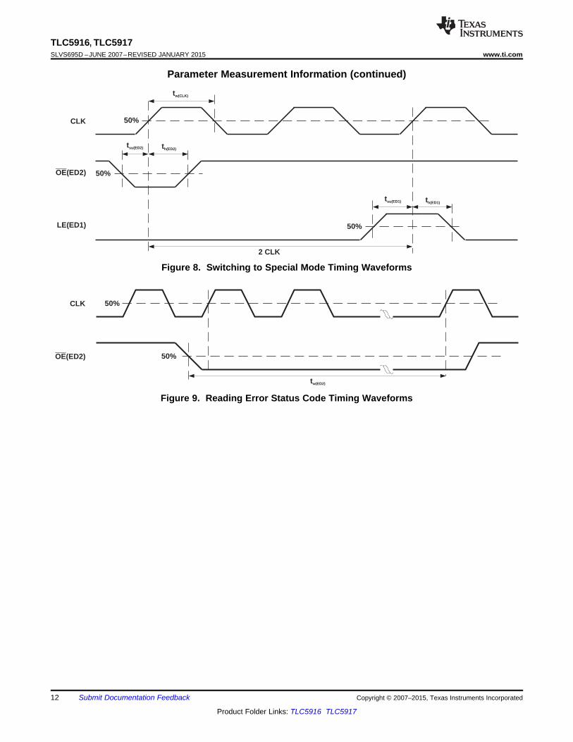
Parameter Measurement Information (continued)
Figure 7. Normal Mode Timing Waveforms
Copyright © 2007–2015, Texas Instruments Incorporated Submit Documentation Feedback 11
Product Folder Links: TLC5916 TLC5917
50%
50%
tw(ED2)
OE(ED2)
CLK
tw(CLK)
tsu(ED2) th(ED2)
OE(ED2)
LE(ED1)
CLK
tsu(ED1) th(ED1)
2 CLK
50%
50%
50%
TLC5916, TLC5917SLVS695D –JUNE 2007–REVISED JANUARY 2015 www.ti.com
Parameter Measurement Information (continued)
Figure 8. Switching to Special Mode Timing Waveforms
Figure 9. Reading Error Status Code Timing Waveforms
12 Submit Documentation Feedback Copyright © 2007–2015, Texas Instruments Incorporated
Product Folder Links: TLC5916 TLC5917

TLC5916, TLC5917www.ti.com SLVS695D –JUNE 2007–REVISED JANUARY 2015
9 Detailed Description
9.1 OverviewThe TLC591x is designed for LED displays and LED lighting applications with constant-current control and open-load, shorted-load, and overtemperature detection. The TLC591x contains an 8-bit shift register and data latches,which convert serial input data into parallel output format. At the output stage, eight regulated current ports aredesigned to provide uniform and constant current for driving LEDs within a wide range of LED Forward Voltage(VF) variations. Used in system design for LED display applications, for example, LED panels, it provides greatflexibility and device performance. Users can adjust the output current from 3 mA to 120 mA per channel throughan external resistor, Rext, which gives flexibility in controlling the light intensity of LEDs. The devices are designedfor up to 20 V at the output port. The high clock frequency, 30 MHz, also satisfies the system requirements ofhigh-volume data transmission.
The TLC591x provides two operation modes: Normal Mode and Special Mode. Normal mode is used for shiftingLED data into and out of the driver. Special Mode includes two functions: Error Detection and Current GainControl. The two operation modes include three phases: Normal Mode phase, Mode Switching transition phase,and Special Mode phase. The signal on the multiple function pin OE(ED2) is monitored to determine the mode.When a one-clock-wide pulse appears on OE(ED2), the device enters the Mode Switching phase. At this time,the voltage level on LE(ED1) determines which mode the TLC591x switches to.
In the Normal Mode phase, the serial data can be transferred into TLC591x through the pin SDI, shifted in theshift register, and transferred out via the pin SDO. LE(ED1) can latch the serial data in the shift register to theoutput latch. OE(ED2) enables the output drivers to sink current.
In the Special Mode phase, the low-voltage-level signal on OE(ED2) can enable output channels and detect thestatus of the output current to determine if the driving current level is sufficient. The detected Error Status isloaded into the 8-bit shift register and shifted out via the pin SDO, synchronous to the CLK signal. The systemcontroller can read the error status and determine if the LEDs are properly lit.
In the Special Mode phase, the TLC591x allows users to adjust the output current level by setting a runtime-programmable Configuration Code. The code is sent into the TLC591x through SDI. The positive pulse ofLE(ED1) latches the code in the shift register into a built-in 8-bit configuration latch, instead of the output latch.The code affects the voltage at the terminal R-EXT and controls the output-current regulator. The output currentcan be finely adjusted by a gain ranging from 1/12 to 127/128 in 256 steps. Therefore, the current skew betweenICs can be compensated within less than 1%. This feature is suitable for white balancing in LED color displaypanels.
Copyright © 2007–2015, Texas Instruments Incorporated Submit Documentation Feedback 13
Product Folder Links: TLC5916 TLC5917

VDD
8
8
8
8
88
I/O Regulator
ControlLogic
OUT0 OUT1 OUT6 OUT7
Output Driver andError Detection
8-Bit OutputLatch
SDOSDI
CLK
LE(ED1)
OE(ED2)
R-EXT
8-Bit ShiftRegister
ConfigurationLatches
TLC5916, TLC5917SLVS695D –JUNE 2007–REVISED JANUARY 2015 www.ti.com
9.2 Functional Block Diagram
9.3 Feature Description
9.3.1 Open-Circuit Detection PrincipleThe LED Open-Circuit Detection compares the effective current level Iout with the open load detection thresholdcurrent IOUT,Th. If IOUT is below the IOUT,Th threshold, the TLC591x detects an open-load condition. This errorstatus can be read as an error status code in the Special Mode. For open-circuit error detection, a channel mustbe on.
Table 1. Open-Circuit DetectionCONDITION OF OUTPUTSTATE OF OUTPUT PORT ERROR STATUS CODE MEANINGCURRENT
Off IOUT = 0 mA 0 Detection not possibleIOUT < IOUT,Th
(1) 0 Open circuitOn
IOUT ≥ IOUT,Th(1) Channel n error status bit 1 Normal
(1) IOUT,Th = 0.5 × IOUT,target (typical)
9.3.2 Short-Circuit Detection Principle (TLC5917 Only)The LED short-circuit detection compares the effective voltage level (VOUT) with the shorted-load detectionthreshold voltages VOUT,TTh and VOUT,RTh. If VOUT is above the VOUT,TTh threshold, the TLC5917 detects anshorted-load condition. If VOUT is below the VOUT,RTh threshold, no error is detected/error bit is reset. This errorstatus can be read as an error status code in the Special Mode. For short-circuit error detection, a channel mustbe on.
14 Submit Documentation Feedback Copyright © 2007–2015, Texas Instruments Incorporated
Product Folder Links: TLC5916 TLC5917

No Fault
Short Fault
MinimumReturn
Threshold
MaximumTrigger
Threshold
3.1 V2.5 V2.2 VVOUT
MinimumTrigger
Threshold
VOUT,TThVOUT,RTh
TLC5916, TLC5917www.ti.com SLVS695D –JUNE 2007–REVISED JANUARY 2015
Table 2. Shorted-Load DetectionCONDITION OF OUTPUTSTATE OF OUTPUT PORT ERROR STATUS CODE MEANINGVOLTAGE
Off IOUT = 0 mA 0 Detection not possibleVOUT ≥ VOUT,TTh 0 Short circuit
OnVOUT < VOUT,RTh 1 Normal
Figure 10. Short-Circuit Detection Principle
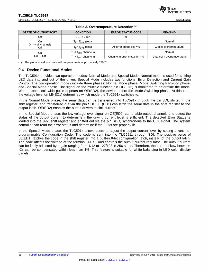
9.3.3 Overtemperature Detection and ShutdownTLC591x is equipped with a global overtemperature sensor and eight individual, channel-specific,overtemperature sensors.• When the global sensor reaches the trip temperature, all output channels are shut down, and the error status
is stored in the internal Error Status register of every channel. After shutdown, the channels automaticallyrestart after cooling down, if the control signal (output latch) remains on. The stored error status is not resetafter cooling down and can be read out as the error status code in the Special Mode.
• When one of the channel-specific sensors reaches trip temperature, only the affected output channel is shutdown, and the error status is stored only in the internal Error Status register of the affected channel. Aftershutdown, the channel automatically restarts after cooling down, if the control signal (output latch) remainson. The stored error status is not reset after cooling down and can be read out as error status code in theSpecial Mode.
For channel-specific overtemperature error detection, a channel must be on.
The error status code is reset when TLC591x returns to Normal Mode.
Copyright © 2007–2015, Texas Instruments Incorporated Submit Documentation Feedback 15
Product Folder Links: TLC5916 TLC5917
TLC5916, TLC5917SLVS695D –JUNE 2007–REVISED JANUARY 2015 www.ti.com
Table 3. Overtemperature Detection (1)
STATE OF OUTPUT PORT CONDITION ERROR STATUS CODE MEANINGOff IOUT = 0 mA 0On Tj < Tj,trip global 1 Normal
On → all channelsTj > Tj,trip global All error status bits = 0 Global overtemperatureOff
Tj < Tj,trip channel n 1 NormalOnOn → Off Tj > Tj,trip channel n Channel n error status bit = 0 Channel n overtemperature
(1) The global shutdown threshold temperature is approximately 170°C.
9.4 Device Functional ModesThe TLC591x provides two operation modes: Normal Mode and Special Mode. Normal mode is used for shiftingLED data into and out of the driver. Special Mode includes two functions: Error Detection and Current GainControl. The two operation modes include three phases: Normal Mode phase, Mode Switching transition phase,and Special Mode phase. The signal on the multiple function pin OE(ED2) is monitored to determine the mode.When a one-clock-wide pulse appears on OE(ED2), the device enters the Mode Switching phase. At this time,the voltage level on LE(ED1) determines which mode the TLC591x switches to.
In the Normal Mode phase, the serial data can be transferred into TLC591x through the pin SDI, shifted in theshift register, and transferred out via the pin SDO. LE(ED1) can latch the serial data in the shift register to theoutput latch. OE(ED2) enables the output drivers to sink current.
In the Special Mode phase, the low-voltage-level signal on OE(ED2) can enable output channels and detect thestatus of the output current to determine if the driving current level is sufficient. The detected Error Status isloaded into the 8-bit shift register and shifted out via the pin SDO, synchronous to the CLK signal. The systemcontroller can read the error status and determine if the LEDs are properly lit.
In the Special Mode phase, the TLC591x allows users to adjust the output current level by setting a runtime-programmable Configuration Code. The code is sent into the TLC591x through SDI. The positive pulse ofLE(ED1) latches the code in the shift register into a built-in 8-bit configuration latch, instead of the output latch.The code affects the voltage at the terminal R-EXT and controls the output-current regulator. The output currentcan be finely adjusted by a gain ranging from 1/12 to 127/128 in 256 steps. Therefore, the current skew betweenICs can be compensated within less than 1%. This feature is suitable for white balancing in LED color displaypanels.
16 Submit Documentation Feedback Copyright © 2007–2015, Texas Instruments Incorporated
Product Folder Links: TLC5916 TLC5917

1 2 3 4 5
1 0 1 1 1
10 0 0 0
CLK
OE(ED2)
LE(ED1)
1 2 30 4 6 75
0
1
off
on
off
on
off
on
off
on
off
on
Don't care
CLK
OE(ED2)
LE(ED1)
SDI
OUT0
OUT1
OUT2
OUT3
OUT7
SDO
TLC5916, TLC5917www.ti.com SLVS695D –JUNE 2007–REVISED JANUARY 2015
Device Functional Modes (continued)
Figure 11. Normal Mode
Table 4. Truth Table in Normal ModeCLK LE(ED1) OE(ED2) SDI OUT0...OUT7 SDO↑ H L Dn Dn...Dn – 7 Dn – 7↑ L L Dn + 1 No change Dn – 6↑ H L Dn + 2 Dn + 2...Dn – 5 Dn – 5↓ X L Dn + 3 Dn + 2...Dn – 5 Dn – 5↓ X H Dn + 3 Off Dn – 5
The signal sequence shown in Figure 12 makes the TLC591x enter Current Adjust and Error Detection Mode.
Figure 12. Switching to Special Mode
In the Current Adjust Mode, sending the positive pulse of LE(ED1), the content of the shift register (a currentadjust code) is written to the 8-bit configuration latch (see Figure 13).
Copyright © 2007–2015, Texas Instruments Incorporated Submit Documentation Feedback 17
Product Folder Links: TLC5916 TLC5917

1 2 3 4 5
1 0 1 1 1
0 0 0 00
CLK
OE(ED2)
LE(ED1)
1 2 3
0
1>2 µs
CLK
OE(ED2)
LE(ED1)
SDO Error Status Code
1 2 30 6 7
1
0
8-bit Configuration Code
CLK
OE(ED2)
LE(ED1)
SDI
TLC5916, TLC5917SLVS695D –JUNE 2007–REVISED JANUARY 2015 www.ti.com
Figure 13. Writing Configuration Code
When the TLC591x is in the Error Detection Mode, the signal sequence shown in Figure 14 enables a systemcontroller to read error status codes through SDO.
Figure 14. Reading Error Status Code
The signal sequence shown in Figure 15 makes TLC591x resume the Normal Mode. Switching to Normal Moderesets all internal Error Status registers. OE(ED2) always enables the output port, whether the TLC591x entersCurrent Adjust Mode or not.
Figure 15. Switching to Normal Mode
9.4.1 Operation Mode SwitchingTo switch between its two modes, TLC591x monitors the signal OE(ED2). When an one-clock-wide pulse ofOE(ED2) appears, TLC591x enters the two-clock-period transition phase, the Mode Switching phase. Afterpower on, the default operation mode is the Normal Mode (see Figure 16).
18 Submit Documentation Feedback Copyright © 2007–2015, Texas Instruments Incorporated
Product Folder Links: TLC5916 TLC5917

1 2 3 4 5
1 0 1 1 1
00 0 0 0
Actual Mode(Normal or Special)
ModeSwitching
NormalMode
CLK
OE(ED2)
LE(ED1)
Phase
1 2 3 4 5
1 0 1 1 1
10 0 0 0
Actual Mode(Normal or Special)
ModeSwitching
SpecialMode
CLK
OE(ED2)
LE(ED1)
Phase
Switching to Special Mode Switching to Normal Mode
TLC5916, TLC5917www.ti.com SLVS695D –JUNE 2007–REVISED JANUARY 2015
Figure 16. Mode Switching
As shown in Figure 16, once a one-clock-wide short pulse (101) of OE(ED2) appears, TLC591x enters the ModeSwitching phase. At the fourth rising edge of CLK, if LE(ED1) is sampled as voltage high, TLC591x switches toSpecial Mode; otherwise, it switches to Normal Mode. The signal LE(ED1) between the third and the fifth risingedges of CLK cannot latch any data. Its level is used only to determine into which mode to switch. However, theshort pulse of OE(ED2) can still enable the output ports. During mode switching, the serial data can still betransferred through SDI and shifted out from SDO.
NOTE1. The signal sequence for the mode switching may be used frequently to ensure that TLC591x is
in the proper mode.2. The 1 and 0 on the LE(ED1) signal are sampled at the rising edge of CLK. The X means its
level does not affect the result of mode switching mechanism.3. After power on, the default operation mode is Normal Mode.
9.4.1.1 Normal Mode PhaseSerial data is transferred into TLC591x through SDI, shifted in the Shift Register, and output via SDO. LE(ED1)can latch the serial data in the Shift Register to the Output Latch. OE(ED2) enables the output drivers to sinkcurrent. These functions differ only as described in Operation Mode Switching, in which case, a short pulsetriggers TLC591x to switch the operation mode. However, as long as LE(ED1) is high in the Mode Switchingphase, TLC591x remains in the Normal Mode, as if no mode switching occurred.
9.4.1.2 Special Mode PhaseIn the Special Mode, as long as OE(ED2) is not low, the serial data is shifted to the Shift Register via SDI andshifted out via SDO, as in the Normal Mode. However, there are two differences between the Special Mode andthe Normal Mode, as shown in the following sections.
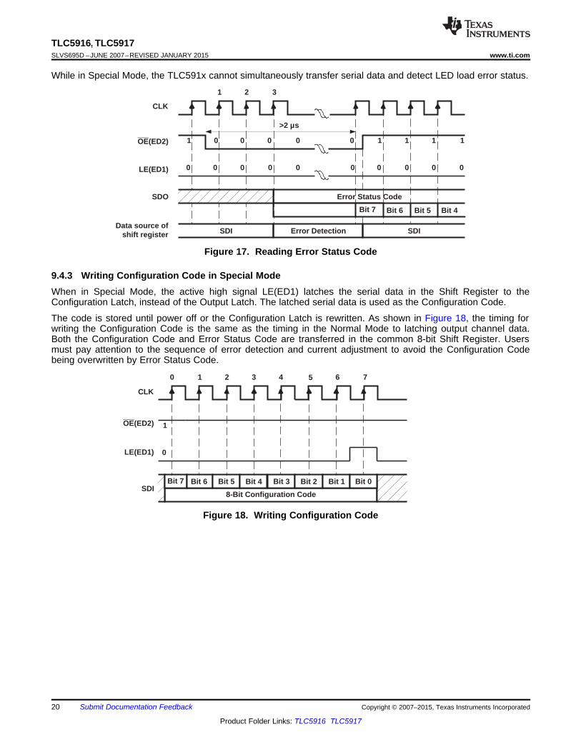
9.4.2 Reading Error Status Code in Special ModeWhen OE(ED2) is pulled low while in Special Mode, error detection and load error status codes are loaded intothe Shift Register, in addition to enabling output ports to sink current. Figure 17 shows the timing sequence forerror detection. The 0 and 1 signal levels are sampled at the rising edge of each CLK. At least three zeros mustbe sampled at the voltage low signal OE(ED2). Immediately after the second zero is sampled, the data inputsource of the Shift Register changes to the 8-bit parallel Error Status Code register, instead of from the serialdata on SDI. Normally, the error status codes are generated at least 2 μs after the falling edge of OE(ED2). Theoccurrence of the third or later zero saves the detected error status codes into the Shift Register. Therefore,when OE(ED2) is low, the serial data cannot be shifted into TLC591x through SDI. When OE(ED2) is pulled high,the data input source of the Shift Register is changed back to SDI. At the same time, the output ports aredisabled and the error detection is completed. Then, the error status codes saved in the Shift Register can beshifted out via SDO bit by bit along with CLK, as well as the new serial data can be shifted into TLC591x throughSDI.
Copyright © 2007–2015, Texas Instruments Incorporated Submit Documentation Feedback 19
Product Folder Links: TLC5916 TLC5917
1 2 30 4 5 6 7
1
0
CLK
OE(ED2)
LE(ED1)
SDI8-Bit Configuration Code
Bit 7 Bit 6 Bit 5 Bit 4 Bit 3 Bit 2 Bit 1 Bit 0
1 2 3
1 0 0 0 1
0 0 0 00
0 0
0 0 0 0
1 1 1
0
CLK
OE(ED2)
LE(ED1)
SDO
Data source ofshift register Error DetectionSDI SDI
Error Status Code
Bit 7 Bit 6 Bit 5 Bit 4
>2 µs
TLC5916, TLC5917SLVS695D –JUNE 2007–REVISED JANUARY 2015 www.ti.com
While in Special Mode, the TLC591x cannot simultaneously transfer serial data and detect LED load error status.
Figure 17. Reading Error Status Code
9.4.3 Writing Configuration Code in Special ModeWhen in Special Mode, the active high signal LE(ED1) latches the serial data in the Shift Register to theConfiguration Latch, instead of the Output Latch. The latched serial data is used as the Configuration Code.
The code is stored until power off or the Configuration Latch is rewritten. As shown in Figure 18, the timing forwriting the Configuration Code is the same as the timing in the Normal Mode to latching output channel data.Both the Configuration Code and Error Status Code are transferred in the common 8-bit Shift Register. Usersmust pay attention to the sequence of error detection and current adjustment to avoid the Configuration Codebeing overwritten by Error Status Code.
Figure 18. Writing Configuration Code
20 Submit Documentation Feedback Copyright © 2007–2015, Texas Instruments Incorporated
Product Folder Links: TLC5916 TLC5917

R ( )ext Ω
I(m
A)
OU
T
0
20
40
60
80
100
120
140
0 1000 2000 3000 4000 5000 6000
TLC5916, TLC5917www.ti.com SLVS695D –JUNE 2007–REVISED JANUARY 2015
10 Application and Implementation
NOTEInformation in the following applications sections is not part of the TI componentspecification, and TI does not warrant its accuracy or completeness. TI’s customers areresponsible for determining suitability of components for their purposes. Customers shouldvalidate and test their design implementation to confirm system functionality.
10.1 Application Information
10.1.1 Constant CurrentIn LED display applications, TLC591x provides nearly no current variations from channel to channel and from ICto IC. While 5 mA ≤ IOUT ≤ 100 mA, the maximum current skew between channels is less than ±3% and betweenICs is less than ±6%.
10.1.2 Adjusting Output CurrentTLC591x scales up the reference current, Iref, set by the external resistor Rext to sink a current, Iout, at eachoutput port. Users can follow the below formulas to calculate the target output current IOUT,target in the saturationregion. In the equations,
Rext is the resistance of the external resistor connected between the R-EXT terminal and ground and VR-EXT is thevoltage of R-EXT, which is controlled by the programmable voltage gain (VG). VG is defined by the ConfigurationCode.
VR-EXT = 1.26 V × VG (1)Iref = VR-EXT/Rext, (2)IOUT,target = Iref × 15 × 3CM – 1 (3)
The Current Multiplier (CM) determines that the ratio IOUT,target/Iref is 15 or 5. After power on, the default value ofVG is 127/128 = 0.992, and the default value of CM is 1, so that the ratio IOUT,target/Iref = 15. Based on the defaultVG and CM:
VR-EXT = 1.26 V × 127/128 = 1.25 V (4)IOUT,target = (1.25 V/Rext) × 15 (5)
Therefore, the default current is approximately 52 mA at 360 Ω and 26 mA at 720 Ω. The default relationshipafter power on between IOUT,target and Rext is shown in Figure 19.
Figure 19. Default Relationship Curve Between IOUT,target and Rext After Power Up
Copyright © 2007–2015, Texas Instruments Incorporated Submit Documentation Feedback 21
Product Folder Links: TLC5916 TLC5917

...
720Ω
VLED
GND
OE
SDO
R-EXT
VDD
LE
CLK
SDI
LE
CLK
OE
SDI
Contr
olle
r
Multiple Cascaded Drivers
26mA Application
VDD: 3.0V to 5.5V
...
OU
T0
OU
T7
TLC
59
17
...
720Ω
GND
OE
SDO
R-EXT
VDD
LE
CLK
SDI
...
OU
T0
OU
T7
TLC
59
17
...
720Ω
GND
OE
SDO
R-EXT
VDD
LE
CLK
SDI
...
OU
T0
OU
T7
TLC
59
17...
Read Back
TLC5916, TLC5917SLVS695D –JUNE 2007–REVISED JANUARY 2015 www.ti.com
Application Information (continued)10.1.3 Cascading Implementation of TLC591x Device
Figure 20. Cascading Implementation of TLC591x Device
22 Submit Documentation Feedback Copyright © 2007–2015, Texas Instruments Incorporated
Product Folder Links: TLC5916 TLC5917
TLC5916, TLC5917www.ti.com SLVS695D –JUNE 2007–REVISED JANUARY 2015
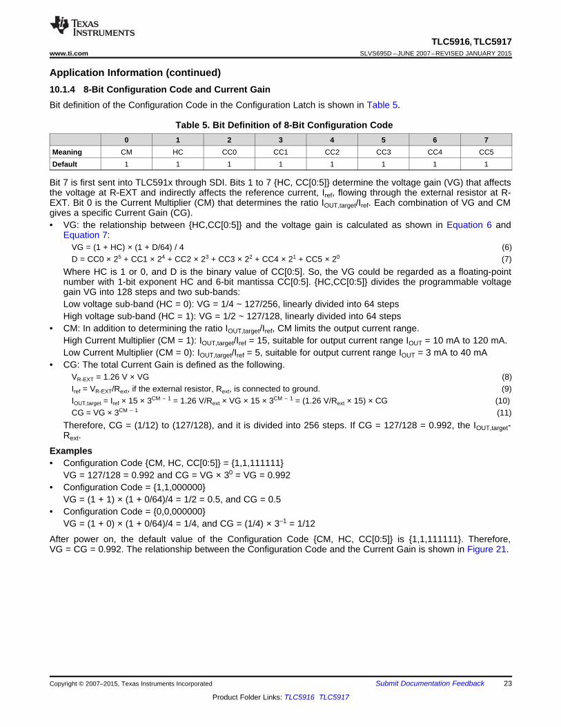
Application Information (continued)10.1.4 8-Bit Configuration Code and Current GainBit definition of the Configuration Code in the Configuration Latch is shown in Table 5.
Table 5. Bit Definition of 8-Bit Configuration Code0 1 2 3 4 5 6 7
Meaning CM HC CC0 CC1 CC2 CC3 CC4 CC5Default 1 1 1 1 1 1 1 1
Bit 7 is first sent into TLC591x through SDI. Bits 1 to 7 HC, CC[0:5] determine the voltage gain (VG) that affectsthe voltage at R-EXT and indirectly affects the reference current, Iref, flowing through the external resistor at R-EXT. Bit 0 is the Current Multiplier (CM) that determines the ratio IOUT,target/Iref. Each combination of VG and CMgives a specific Current Gain (CG).• VG: the relationship between HC,CC[0:5] and the voltage gain is calculated as shown in Equation 6 and
Equation 7:VG = (1 + HC) × (1 + D/64) / 4 (6)D = CC0 × 25 + CC1 × 24 + CC2 × 23 + CC3 × 22 + CC4 × 21 + CC5 × 20 (7)
Where HC is 1 or 0, and D is the binary value of CC[0:5]. So, the VG could be regarded as a floating-pointnumber with 1-bit exponent HC and 6-bit mantissa CC[0:5]. HC,CC[0:5] divides the programmable voltagegain VG into 128 steps and two sub-bands:Low voltage sub-band (HC = 0): VG = 1/4 ~ 127/256, linearly divided into 64 stepsHigh voltage sub-band (HC = 1): VG = 1/2 ~ 127/128, linearly divided into 64 steps
• CM: In addition to determining the ratio IOUT,target/Iref, CM limits the output current range.High Current Multiplier (CM = 1): IOUT,target/Iref = 15, suitable for output current range IOUT = 10 mA to 120 mA.Low Current Multiplier (CM = 0): IOUT,target/Iref = 5, suitable for output current range IOUT = 3 mA to 40 mA
• CG: The total Current Gain is defined as the following.VR-EXT = 1.26 V × VG (8)Iref = VR-EXT/Rext, if the external resistor, Rext, is connected to ground. (9)IOUT,target = Iref × 15 × 3CM – 1 = 1.26 V/Rext × VG × 15 × 3CM – 1 = (1.26 V/Rext × 15) × CG (10)CG = VG × 3CM – 1 (11)
Therefore, CG = (1/12) to (127/128), and it is divided into 256 steps. If CG = 127/128 = 0.992, the IOUT,target-Rext.
Examples• Configuration Code CM, HC, CC[0:5] = 1,1,111111
VG = 127/128 = 0.992 and CG = VG × 30 = VG = 0.992• Configuration Code = 1,1,000000
VG = (1 + 1) × (1 + 0/64)/4 = 1/2 = 0.5, and CG = 0.5• Configuration Code = 0,0,000000
VG = (1 + 0) × (1 + 0/64)/4 = 1/4, and CG = (1/4) × 3–1 = 1/12
After power on, the default value of the Configuration Code CM, HC, CC[0:5] is 1,1,111111. Therefore,VG = CG = 0.992. The relationship between the Configuration Code and the Current Gain is shown in Figure 21.
Copyright © 2007–2015, Texas Instruments Incorporated Submit Documentation Feedback 23
Product Folder Links: TLC5916 TLC5917

. . .
VLED
GND
SDO
R-EXT
VDD
LE
CLK
SDI
LE
CLK
OE OE
SDI
Contr
oller
OU
T0
. . .
3.0V to 5.5V
OU
T1
OU
T6
OU
T7
TLC5917To Controller if Error
Detection Used
1.00
0.00
0.50
0.25
0.75
CM = 0 (Low Current Multiplier)
HC = 1 (HighVoltage SubBand)
HC = 0 (LowVoltage SubBand)
HC = 0 (LowVoltage SubBand)
HC = 1 (HighVoltage SubBand)
CM = 1 (High Current Multiplier)
Configuration Code (CM, HC, CC[0:5]) in Binary Format
Cu
rren
t G
ain
(C
G)
TLC5916, TLC5917SLVS695D –JUNE 2007–REVISED JANUARY 2015 www.ti.com
Figure 21. Current Gain vs Configuration Code
10.2 Typical ApplicationFigure 22 shows implementation of a single TLC591x device. Figure 20 shows a cascaded driverimplementation.
Figure 22. Single Implementation of TLC591x Device
24 Submit Documentation Feedback Copyright © 2007–2015, Texas Instruments Incorporated
Product Folder Links: TLC5916 TLC5917

TLC5916, TLC5917www.ti.com SLVS695D –JUNE 2007–REVISED JANUARY 2015
Typical Application (continued)10.2.1 Design RequirementsFor this design example, use the parameters listed in Table 6. The purpose of this design procedure is tocalculate the power dissipation in the device and the operating junction temperature.
Table 6. Design ParametersDESIGN PARAMETERS EXAMPLE VALUE
Number of LED strings 8Number of LEDs per string 3LED Current (mA) 20Forward voltage of each LED (V) 3.5Junction-to-ambient thermal resistance (°C/W) 87.4Ambient temperature of application (°C) 115VDD (V) 5IDD (mA) 10Max operating junction temperature (°C) 150
10.2.2 Detailed Design ProcedureTJ = TA + RθJA × PD_TOT
where• TJ is the junction temperature.• TA is the ambient temperature.• RθJA is the junction-to-ambient thermal resistance.• PD_TOT is the total power dissipation in the IC. (12)
PD_TOT = PD_CS + IDD × VDD
where• PD_CSis the power dissipation in the LED current sinks.• IDD is the IC supply current.• VDD is the IC supply voltage. (13)
PD_CS = IO × VO × nCH
where• IO is the LED current.• VO is the voltage at the output pin.• nCH is the number of LED strings. (14)
VO = VLED – (nLED × VF)
where• VLED is the voltage applied to the LED string.• nLED is the number of LEDs in the string.• VF is the forward voltage of each LED. (15)
VO must not be too high as this causes excess power dissipation inside the current sink. However, VO also mustnot be too low as this does not allow the full LED current (Figure 4). With VLED = 12 V:
VO = 12 V – (3 × 3.5 V) = 1.5 V (16)PD_CS = 20 mA × 1.5 V × 8 = 0.24 W (17)
Using PD_CS, calculate:PD_TOT = PD_CS + IDD × VDD = 0.24 W + 0.01 A × 5 V = 0.29 W (18)
Using PD_TOT, calculate:TJ = TA + RθJA × PD_TOT = 115°C + 87.4°C/W × 0.29 W = 140°C (19)
Copyright © 2007–2015, Texas Instruments Incorporated Submit Documentation Feedback 25
Product Folder Links: TLC5916 TLC5917

0
25
50
75
100
125
150
0 0.5 1 1.5 2 2.5 3
Output Voltage (V)
Ou
tpu
tC
urr
en
t(m
A)
Temperature = 25°C
IO = 80 mA
IO = 40 mA
IO = 20 mA
IO = 60 mA
IO = 5 mA
IO = 100 mA
IO = 120 mA
TLC5916, TLC5917SLVS695D –JUNE 2007–REVISED JANUARY 2015 www.ti.com
This design example demonstrates how to calculate power dissipation in the IC and ensure that the junctiontemperature is kept below 150°C.
NOTEThis design example assumes that all channels have the same electrical parameters(nLED, IO, VF, VLED). If the parameters are unique for each channel, then the powerdissipation must be calculated for each current sink separately. Then, each result must beadded together to calculate the total power dissipation in the current sinks.
10.2.3 Application Curve
Figure 23. Output Current vs Output Voltage
26 Submit Documentation Feedback Copyright © 2007–2015, Texas Instruments Incorporated
Product Folder Links: TLC5916 TLC5917

GND
SDI
CLK
LE(ED1)
OUT0
OUT1
OUT2
OUT3 OUT4
OUT5
OUT6
OUT7
OE(ED2)
SDO
R-EXT
VDD
VIA to GND
To µC
To µC
To µC
To µC
To µC
VDD
VLED
TLC5916, TLC5917www.ti.com SLVS695D –JUNE 2007–REVISED JANUARY 2015
11 Power Supply RecommendationsThe device is designed to operate from a VDD supply between 3 V and 5.5 V. The LED supply voltage isdetermined by the number of LEDs in each string and the forward voltage of the LEDs.
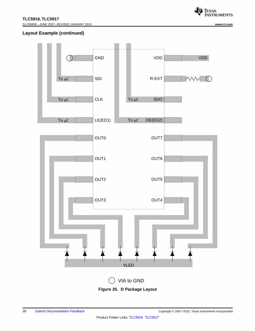
12 Layout
12.1 Layout GuidelinesThe traces that carry current from the LED cathodes to the OUTx pins must be wide enough to support thedefault current (up to 120 mA).
The SDI, CLK, LE (ED1), OE (ED2), and SDO pins are to be connected to the microcontroller. There are severalways to achieve this, including the following methods:• Traces may be routed underneath the package on the top layer.• The signal may travel through a via to another layer.
12.2 Layout Example
Figure 24. PW Package Layout
Copyright © 2007–2015, Texas Instruments Incorporated Submit Documentation Feedback 27
Product Folder Links: TLC5916 TLC5917
GND
SDI
CLK
LE(ED1)
OUT0
OUT1
OUT2
OUT3 OUT4
OUT5
OUT6
OUT7
OE(ED2)
SDO
R-EXT
VDD
VLED
VIA to GND
To µC To µC
VDD
To µCTo µC
To µC
TLC5916, TLC5917SLVS695D –JUNE 2007–REVISED JANUARY 2015 www.ti.com
Layout Example (continued)
Figure 25. D Package Layout
28 Submit Documentation Feedback Copyright © 2007–2015, Texas Instruments Incorporated
Product Folder Links: TLC5916 TLC5917

TLC5916, TLC5917www.ti.com SLVS695D –JUNE 2007–REVISED JANUARY 2015
13 Device and Documentation Support
13.1 Related LinksThe table below lists quick access links. Categories include technical documents, support and communityresources, tools and software, and quick access to sample or buy.
Table 7. Related LinksTECHNICAL TOOLS & SUPPORT &PARTS PRODUCT FOLDER SAMPLE & BUY DOCUMENTS SOFTWARE COMMUNITY
TLC5916 Click here Click here Click here Click here Click hereTLC5917 Click here Click here Click here Click here Click here
13.2 TrademarksAll trademarks are the property of their respective owners.
13.3 Electrostatic Discharge CautionThese devices have limited built-in ESD protection. The leads should be shorted together or the device placed in conductive foamduring storage or handling to prevent electrostatic damage to the MOS gates.
13.4 GlossarySLYZ022 — TI Glossary.
This glossary lists and explains terms, acronyms, and definitions.
14 Mechanical, Packaging, and Orderable InformationThe following pages include mechanical, packaging, and orderable information. This information is the mostcurrent data available for the designated devices. This data is subject to change without notice and revision ofthis document. For browser-based versions of this data sheet, refer to the left-hand navigation.
Copyright © 2007–2015, Texas Instruments Incorporated Submit Documentation Feedback 29
Product Folder Links: TLC5916 TLC5917

PACKAGE OPTION ADDENDUM
www.ti.com 1-Oct-2014
Addendum-Page 1
PACKAGING INFORMATION
Orderable Device Status(1)
Package Type PackageDrawing
Pins PackageQty
Eco Plan(2)
Lead/Ball Finish(6)
MSL Peak Temp(3)
Op Temp (°C) Device Marking(4/5)
Samples
TLC5916ID ACTIVE SOIC D 16 40 Green (RoHS& no Sb/Br)
CU NIPDAU Level-1-260C-UNLIM -40 to 125 TLC5916I
TLC5916IDG4 ACTIVE SOIC D 16 40 Green (RoHS& no Sb/Br)
CU NIPDAU Level-1-260C-UNLIM -40 to 125 TLC5916I
TLC5916IDR ACTIVE SOIC D 16 2500 Green (RoHS& no Sb/Br)
CU NIPDAU Level-1-260C-UNLIM -40 to 125 TLC5916I
TLC5916IDRG4 ACTIVE SOIC D 16 2500 Green (RoHS& no Sb/Br)
CU NIPDAU Level-1-260C-UNLIM -40 to 125 TLC5916I
TLC5916IN ACTIVE PDIP N 16 25 Pb-Free(RoHS)
CU NIPDAU N / A for Pkg Type -40 to 125 TLC5916IN
TLC5916INE4 ACTIVE PDIP N 16 25 Pb-Free(RoHS)
CU NIPDAU N / A for Pkg Type -40 to 125 TLC5916IN
TLC5916IPW ACTIVE TSSOP PW 16 90 Green (RoHS& no Sb/Br)
CU NIPDAU Level-1-260C-UNLIM -40 to 125 Y5916
TLC5916IPWG4 ACTIVE TSSOP PW 16 90 Green (RoHS& no Sb/Br)
CU NIPDAU Level-1-260C-UNLIM -40 to 125 Y5916
TLC5916IPWR ACTIVE TSSOP PW 16 2000 Green (RoHS& no Sb/Br)
CU NIPDAU Level-1-260C-UNLIM -40 to 125 Y5916
TLC5916IPWRG4 ACTIVE TSSOP PW 16 2000 Green (RoHS& no Sb/Br)
CU NIPDAU Level-1-260C-UNLIM -40 to 125 Y5916
TLC5917ID ACTIVE SOIC D 16 40 Green (RoHS& no Sb/Br)
CU NIPDAU Level-1-260C-UNLIM -40 to 125 TLC5917I
TLC5917IDR ACTIVE SOIC D 16 2500 Green (RoHS& no Sb/Br)
CU NIPDAU Level-1-260C-UNLIM -40 to 125 TLC5917I
TLC5917IDRG4 ACTIVE SOIC D 16 2500 Green (RoHS& no Sb/Br)
CU NIPDAU Level-1-260C-UNLIM -40 to 125 TLC5917I
TLC5917IN ACTIVE PDIP N 16 25 Pb-Free(RoHS)
CU NIPDAU N / A for Pkg Type -40 to 125 TLC5917IN
TLC5917INE4 ACTIVE PDIP N 16 25 Pb-Free(RoHS)
CU NIPDAU N / A for Pkg Type -40 to 125 TLC5917IN
TLC5917IPW ACTIVE TSSOP PW 16 90 Green (RoHS& no Sb/Br)
CU NIPDAU Level-1-260C-UNLIM -40 to 125 Y5917
TLC5917IPWR ACTIVE TSSOP PW 16 2000 Green (RoHS& no Sb/Br)
CU NIPDAU Level-1-260C-UNLIM -40 to 125 Y5917

PACKAGE OPTION ADDENDUM
www.ti.com 1-Oct-2014
Addendum-Page 2
Orderable Device Status(1)
Package Type PackageDrawing
Pins PackageQty
Eco Plan(2)
Lead/Ball Finish(6)
MSL Peak Temp(3)
Op Temp (°C) Device Marking(4/5)
Samples
TLC5917IPWRG4 ACTIVE TSSOP PW 16 2000 Green (RoHS& no Sb/Br)
CU NIPDAU Level-1-260C-UNLIM -40 to 125 Y5917
(1) The marketing status values are defined as follows:ACTIVE: Product device recommended for new designs.LIFEBUY: TI has announced that the device will be discontinued, and a lifetime-buy period is in effect.NRND: Not recommended for new designs. Device is in production to support existing customers, but TI does not recommend using this part in a new design.PREVIEW: Device has been announced but is not in production. Samples may or may not be available.OBSOLETE: TI has discontinued the production of the device.
(2) Eco Plan - The planned eco-friendly classification: Pb-Free (RoHS), Pb-Free (RoHS Exempt), or Green (RoHS & no Sb/Br) - please check http://www.ti.com/productcontent for the latest availabilityinformation and additional product content details.TBD: The Pb-Free/Green conversion plan has not been defined.Pb-Free (RoHS): TI's terms "Lead-Free" or "Pb-Free" mean semiconductor products that are compatible with the current RoHS requirements for all 6 substances, including the requirement thatlead not exceed 0.1% by weight in homogeneous materials. Where designed to be soldered at high temperatures, TI Pb-Free products are suitable for use in specified lead-free processes.Pb-Free (RoHS Exempt): This component has a RoHS exemption for either 1) lead-based flip-chip solder bumps used between the die and package, or 2) lead-based die adhesive used betweenthe die and leadframe. The component is otherwise considered Pb-Free (RoHS compatible) as defined above.Green (RoHS & no Sb/Br): TI defines "Green" to mean Pb-Free (RoHS compatible), and free of Bromine (Br) and Antimony (Sb) based flame retardants (Br or Sb do not exceed 0.1% by weightin homogeneous material)
(3) MSL, Peak Temp. - The Moisture Sensitivity Level rating according to the JEDEC industry standard classifications, and peak solder temperature.
(4) There may be additional marking, which relates to the logo, the lot trace code information, or the environmental category on the device.
(5) Multiple Device Markings will be inside parentheses. Only one Device Marking contained in parentheses and separated by a "~" will appear on a device. If a line is indented then it is a continuationof the previous line and the two combined represent the entire Device Marking for that device.
(6) Lead/Ball Finish - Orderable Devices may have multiple material finish options. Finish options are separated by a vertical ruled line. Lead/Ball Finish values may wrap to two lines if the finishvalue exceeds the maximum column width.
Important Information and Disclaimer:The information provided on this page represents TI's knowledge and belief as of the date that it is provided. TI bases its knowledge and belief on informationprovided by third parties, and makes no representation or warranty as to the accuracy of such information. Efforts are underway to better integrate information from third parties. TI has taken andcontinues to take reasonable steps to provide representative and accurate information but may not have conducted destructive testing or chemical analysis on incoming materials and chemicals.TI and TI suppliers consider certain information to be proprietary, and thus CAS numbers and other limited information may not be available for release.
In no event shall TI's liability arising out of such information exceed the total purchase price of the TI part(s) at issue in this document sold by TI to Customer on an annual basis.
OTHER QUALIFIED VERSIONS OF TLC5916, TLC5917 :

PACKAGE OPTION ADDENDUM
www.ti.com 1-Oct-2014
Addendum-Page 3
• Automotive: TLC5916-Q1, TLC5917-Q1
NOTE: Qualified Version Definitions:
• Automotive - Q100 devices qualified for high-reliability automotive applications targeting zero defects

TAPE AND REEL INFORMATION
*All dimensions are nominal
Device PackageType
PackageDrawing
Pins SPQ ReelDiameter
(mm)
ReelWidth
W1 (mm)
A0(mm)
B0(mm)
K0(mm)
P1(mm)
W(mm)
Pin1Quadrant
TLC5916IDR SOIC D 16 2500 330.0 16.4 6.5 10.3 2.1 8.0 16.0 Q1
TLC5916IPWR TSSOP PW 16 2000 330.0 12.4 6.9 5.6 1.6 8.0 12.0 Q1
TLC5917IDR SOIC D 16 2500 330.0 16.4 6.5 10.3 2.1 8.0 16.0 Q1
TLC5917IPWR TSSOP PW 16 2000 330.0 12.4 6.9 5.6 1.6 8.0 12.0 Q1
PACKAGE MATERIALS INFORMATION
www.ti.com 1-Oct-2014
Pack Materials-Page 1

*All dimensions are nominal
Device Package Type Package Drawing Pins SPQ Length (mm) Width (mm) Height (mm)
TLC5916IDR SOIC D 16 2500 333.2 345.9 28.6
TLC5916IPWR TSSOP PW 16 2000 367.0 367.0 35.0
TLC5917IDR SOIC D 16 2500 333.2 345.9 28.6
TLC5917IPWR TSSOP PW 16 2000 367.0 367.0 35.0
PACKAGE MATERIALS INFORMATION
www.ti.com 1-Oct-2014
Pack Materials-Page 2


IMPORTANT NOTICE
Texas Instruments Incorporated and its subsidiaries (TI) reserve the right to make corrections, enhancements, improvements and otherchanges to its semiconductor products and services per JESD46, latest issue, and to discontinue any product or service per JESD48, latestissue. Buyers should obtain the latest relevant information before placing orders and should verify that such information is current andcomplete. All semiconductor products (also referred to herein as “components”) are sold subject to TI’s terms and conditions of salesupplied at the time of order acknowledgment.TI warrants performance of its components to the specifications applicable at the time of sale, in accordance with the warranty in TI’s termsand conditions of sale of semiconductor products. Testing and other quality control techniques are used to the extent TI deems necessaryto support this warranty. Except where mandated by applicable law, testing of all parameters of each component is not necessarilyperformed.TI assumes no liability for applications assistance or the design of Buyers’ products. Buyers are responsible for their products andapplications using TI components. To minimize the risks associated with Buyers’ products and applications, Buyers should provideadequate design and operating safeguards.TI does not warrant or represent that any license, either express or implied, is granted under any patent right, copyright, mask work right, orother intellectual property right relating to any combination, machine, or process in which TI components or services are used. Informationpublished by TI regarding third-party products or services does not constitute a license to use such products or services or a warranty orendorsement thereof. Use of such information may require a license from a third party under the patents or other intellectual property of thethird party, or a license from TI under the patents or other intellectual property of TI.Reproduction of significant portions of TI information in TI data books or data sheets is permissible only if reproduction is without alterationand is accompanied by all associated warranties, conditions, limitations, and notices. TI is not responsible or liable for such altereddocumentation. Information of third parties may be subject to additional restrictions.Resale of TI components or services with statements different from or beyond the parameters stated by TI for that component or servicevoids all express and any implied warranties for the associated TI component or service and is an unfair and deceptive business practice.TI is not responsible or liable for any such statements.Buyer acknowledges and agrees that it is solely responsible for compliance with all legal, regulatory and safety-related requirementsconcerning its products, and any use of TI components in its applications, notwithstanding any applications-related information or supportthat may be provided by TI. Buyer represents and agrees that it has all the necessary expertise to create and implement safeguards whichanticipate dangerous consequences of failures, monitor failures and their consequences, lessen the likelihood of failures that might causeharm and take appropriate remedial actions. Buyer will fully indemnify TI and its representatives against any damages arising out of the useof any TI components in safety-critical applications.In some cases, TI components may be promoted specifically to facilitate safety-related applications. With such components, TI’s goal is tohelp enable customers to design and create their own end-product solutions that meet applicable functional safety standards andrequirements. Nonetheless, such components are subject to these terms.No TI components are authorized for use in FDA Class III (or similar life-critical medical equipment) unless authorized officers of the partieshave executed a special agreement specifically governing such use.Only those TI components which TI has specifically designated as military grade or “enhanced plastic” are designed and intended for use inmilitary/aerospace applications or environments. Buyer acknowledges and agrees that any military or aerospace use of TI componentswhich have not been so designated is solely at the Buyer's risk, and that Buyer is solely responsible for compliance with all legal andregulatory requirements in connection with such use.TI has specifically designated certain components as meeting ISO/TS16949 requirements, mainly for automotive use. In any case of use ofnon-designated products, TI will not be responsible for any failure to meet ISO/TS16949.
Products ApplicationsAudio www.ti.com/audio Automotive and Transportation www.ti.com/automotiveAmplifiers amplifier.ti.com Communications and Telecom www.ti.com/communicationsData Converters dataconverter.ti.com Computers and Peripherals www.ti.com/computersDLP® Products www.dlp.com Consumer Electronics www.ti.com/consumer-appsDSP dsp.ti.com Energy and Lighting www.ti.com/energyClocks and Timers www.ti.com/clocks Industrial www.ti.com/industrialInterface interface.ti.com Medical www.ti.com/medicalLogic logic.ti.com Security www.ti.com/securityPower Mgmt power.ti.com Space, Avionics and Defense www.ti.com/space-avionics-defenseMicrocontrollers microcontroller.ti.com Video and Imaging www.ti.com/videoRFID www.ti-rfid.comOMAP Applications Processors www.ti.com/omap TI E2E Community e2e.ti.comWireless Connectivity www.ti.com/wirelessconnectivity
Mailing Address: Texas Instruments, Post Office Box 655303, Dallas, Texas 75265Copyright © 2015, Texas Instruments Incorporated