TL071 Data Sheet – Texas Instruments - TI. · PDF fileTL071, TL071A, TL071B TL072,...
67
+ - + - IN+ IN- OUT IN+ IN- OUT TL072 (each amplifier) TL074 (each amplifier) TL071 OFFSET N1 OFFSET N2 Copyright © 2017, Texas Instruments Incorporated Product Folder Order Now Technical Documents Tools & Software Support & Community An IMPORTANT NOTICE at the end of this data sheet addresses availability, warranty, changes, use in safety-critical applications, intellectual property matters and other important disclaimers. PRODUCTION DATA. TL071, TL071A, TL071B TL072, TL072A, TL072B, TL074, TL074A, TL074B, TL072M, TL074M SLOS080N – SEPTEMBER 1978 – REVISED JULY 2017 TL07xx Low-Noise JFET-Input Operational Amplifiers 1 1 Features 1• Low Power Consumption • Wide Common-Mode and Differential Voltage Ranges • Low Input Bias and Offset Currents • Output Short-Circuit Protection • Low Total Harmonic Distortion: 0.003% (Typical) • Low Noise V n = 18 nV/√Hz (Typical) at f = 1 kHz • High-Input Impedance: JFET Input Stage • Internal Frequency Compensation • Latch-Up-Free Operation • High Slew Rate: 13 V/μs (Typical) • Common-Mode Input Voltage Range Includes V CC+ 2 Applications • Motor Integrated Systems: UPS • Drives and Control Solutions: AC Inverter and VF Drives • Renewables: Solar Inverters • Pro Audio Mixers • DLP Front Projection System • Oscilloscopes 3 Description The TL07xx JFET-input operational amplifiers incorporate well-matched, high-voltage JFET and bipolar transistors in a monolithic integrated circuit. The devices feature high slew rates, low-input bias and offset currents, and low offset-voltage temperature coefficient. The low harmonic distortion and low noise make the TL07x series ideally suited for high-fidelity and audio pre-amplifier applications. The TL071 device has offset pins to support external input offset correction. Device Information (1) PART NUMBER PACKAGE BODY SIZE (NOM) TL07xxD SOIC (14) 8.65 mm × 3.91 mm SOIC (8) 4.90 mm x 3.90 mm TL07xxJG CDIP (8) 9.59 mm x 6.67 mm TL074xJ CDIP (14) 19.56 mm × 6.92 mm TL07xxP PDIP (8) 9.59 mm x 6.35 mm TL07xxPS SO (8) 6.20 mm x 5.30 mm TL074xN PDIP (14) 19.3 mm × 6.35 mm TL074xNS SO (14) 10.30 mm × 5.30 mm TL07xxPW TSSOP (8) 4.40 mm x 3.00 mm TL074xPW TSSOP (14) 5.00 mm × 4.40 mm (1) For all available packages, see the orderable addendum at the end of the data sheet. Logic Symbols
Transcript of TL071 Data Sheet – Texas Instruments - TI. · PDF fileTL071, TL071A, TL071B TL072,...

+
−
+
−
IN+
IN−
OUT
IN+
IN−
OUT
TL072 (each amplifier)TL074 (each amplifier)
TL071
OFFSET N1
OFFSET N2 Copyright © 2017, Texas Instruments Incorporated
Product
Folder
Order
Now
Technical
Documents
Tools &
Software
Support &Community
An IMPORTANT NOTICE at the end of this data sheet addresses availability, warranty, changes, use in safety-critical applications,intellectual property matters and other important disclaimers. PRODUCTION DATA.
TL071, TL071A, TL071BTL072, TL072A, TL072B, TL074, TL074A, TL074B, TL072M, TL074M
SLOS080N –SEPTEMBER 1978–REVISED JULY 2017
TL07xx Low-Noise JFET-Input Operational Amplifiers
1
1 Features1• Low Power Consumption• Wide Common-Mode and Differential Voltage
Ranges• Low Input Bias and Offset Currents• Output Short-Circuit Protection• Low Total Harmonic Distortion: 0.003% (Typical)• Low Noise
Vn = 18 nV/√Hz (Typical) at f = 1 kHz• High-Input Impedance: JFET Input Stage• Internal Frequency Compensation• Latch-Up-Free Operation• High Slew Rate: 13 V/μs (Typical)• Common-Mode Input Voltage Range
Includes VCC+
2 Applications• Motor Integrated Systems: UPS• Drives and Control Solutions: AC Inverter and VF
Drives• Renewables: Solar Inverters• Pro Audio Mixers• DLP Front Projection System• Oscilloscopes
3 DescriptionThe TL07xx JFET-input operational amplifiersincorporate well-matched, high-voltage JFET andbipolar transistors in a monolithic integrated circuit.The devices feature high slew rates, low-input biasand offset currents, and low offset-voltagetemperature coefficient. The low harmonic distortionand low noise make the TL07x series ideally suitedfor high-fidelity and audio pre-amplifier applications.The TL071 device has offset pins to support externalinput offset correction.
Device Information(1)
PART NUMBER PACKAGE BODY SIZE (NOM)
TL07xxDSOIC (14) 8.65 mm × 3.91 mmSOIC (8) 4.90 mm x 3.90 mm
TL07xxJG CDIP (8) 9.59 mm x 6.67 mmTL074xJ CDIP (14) 19.56 mm × 6.92 mmTL07xxP PDIP (8) 9.59 mm x 6.35 mmTL07xxPS SO (8) 6.20 mm x 5.30 mmTL074xN PDIP (14) 19.3 mm × 6.35 mmTL074xNS SO (14) 10.30 mm × 5.30 mmTL07xxPW TSSOP (8) 4.40 mm x 3.00 mmTL074xPW TSSOP (14) 5.00 mm × 4.40 mm
(1) For all available packages, see the orderable addendum atthe end of the data sheet.
Logic Symbols
2
TL071, TL071A, TL071BTL072, TL072A, TL072B, TL074, TL074A, TL074B, TL072M, TL074MSLOS080N –SEPTEMBER 1978–REVISED JULY 2017 www.ti.com
Product Folder Links: TL071 TL071A TL071B TL072 TL072A TL072B TL074 TL074A TL074B TL072M TL074M
Submit Documentation Feedback Copyright © 1978–2017, Texas Instruments Incorporated
Table of Contents1 Features .................................................................. 12 Applications ........................................................... 13 Description ............................................................. 14 Revision History..................................................... 25 Pin Configuration and Functions ......................... 46 Specifications....................................................... 10
6.1 Absolute Maximum Ratings .................................... 106.2 ESD Ratings............................................................ 106.3 Recommended Operating Conditions..................... 106.4 Thermal Information: TL071x.................................. 116.5 Thermal Information: TL072x.................................. 116.6 Thermal Information: TL072x (cont.)....................... 116.7 Thermal Information: TL074x.................................. 116.8 Thermal Information: TL074x (cont)........................ 126.9 Thermal Information: TL074x (cont)........................ 126.10 Electrical Characteristics: TL071C, TL072C,
TL074C .................................................................... 136.11 Electrical Characteristics: TL071AC, TL072AC,
TL074AC.................................................................. 146.12 Electrical Characteristics: TL071BC, TL072BC,
TL074BC.................................................................. 156.13 Electrical Characteristics: TL071I, TL072I,
TL074I ...................................................................... 166.14 Electrical Characteristics: TL071M, TL072M ........ 176.15 Electrical Characteristics: TL074M ....................... 186.16 Switching Characteristics: TL07xM....................... 196.17 Switching Characteristics: TL07xC, TL07xAC,
TL07xBC, TL07xI ..................................................... 196.18 Typical Characteristics .......................................... 206.1 Parameter Measurement Information ..................... 25
7 Detailed Description ............................................ 267.1 Overview ................................................................. 267.2 Functional Block Diagram ....................................... 267.3 Feature Description................................................. 277.4 Device Functional Modes........................................ 27
8 Application and Implementation ........................ 288.1 Application Information............................................ 288.2 Typical Application .................................................. 288.3 Unity Gain Buffer..................................................... 298.4 System Examples ................................................... 30
9 Power Supply Recommendations ...................... 3210 Layout................................................................... 32
10.1 Layout Guidelines ................................................. 3210.2 Layout Example .................................................... 33
11 Device and Documentation Support ................. 3411.1 Documentation Support ........................................ 3411.2 Related Links ........................................................ 3411.3 Community Resources.......................................... 3411.4 Trademarks ........................................................... 3411.5 Electrostatic Discharge Caution............................ 3411.6 Glossary ................................................................ 34
12 Mechanical, Packaging, and OrderableInformation ........................................................... 35
4 Revision HistoryNOTE: Page numbers for previous revisions may differ from page numbers in the current version.
Changes from Revision M (February 2014) to Revision N Page
• Updated data sheet text to latest documentation and translation standards ......................................................................... 1• Added TL072M and TL074M devices to data sheet ............................................................................................................. 1• Rewrote text in Description section ....................................................................................................................................... 1• Changed TL07x 8-pin PDIP package to 8-pin CDIP package in Device Information table .................................................. 1• Deleted 20-pin LCCC package from Device Information table ............................................................................................. 1• Added 2017 copyright statement to front page schematic ..................................................................................................... 1• Deleted TL071x FK (LCCC) pinout drawing and pinout table in Pin Configurations and Functions section ........................ 4• Updated pinout diagrams and pinout tables in Pin Configurations and Functions section ................................................... 5• Deleted differential input voltage parameter from Absolute Maximum Ratings table ......................................................... 10• Deleted table notes from Absolute Maximum Ratings table ............................................................................................... 10• Added new table note to Absolute Maximum Ratings table ................................................................................................ 10• Changed minimum supply voltage value from –18 V to –0.3 V in Absolute Maximum Ratings table ................................. 10• Changed maximum supply voltage from 18 V to 36 V in Absolute Maximum Ratings table ............................................... 10• Changed minimum input voltage value from –15 V to VCC– – 0.3 V in Absolute Maximum Ratings table........................... 10• Changed maximum input voltage from 15 V to VCC– + 36 V in Absolute Maximum Ratings table....................................... 10• Added input clamp current parameter to Absolute Maximum Ratings table ....................................................................... 10• Changed common-mode voltage maximum value from VCC+ – 4 V to VCC+ in the Recommended Operating
Conditions table .................................................................................................................................................................... 10

3
TL071, TL071A, TL071BTL072, TL072A, TL072B, TL074, TL074A, TL074B, TL072M, TL074M
www.ti.com SLOS080N –SEPTEMBER 1978–REVISED JULY 2017
Product Folder Links: TL071 TL071A TL071B TL072 TL072A TL072B TL074 TL074A TL074B TL072M TL074M
Submit Documentation FeedbackCopyright © 1978–2017, Texas Instruments Incorporated
Revision History (continued)• Changed devices in Recommended Operating Conditions table from TL07xA and TL07xB to TL07xAC and
TL07xBC .............................................................................................................................................................................. 10• Added TL07xI operating free-air temperature minimum value of –40°C to Recommended Operating Conditions table ... 10• Added U (CFP) package thermal values to Thermal Information: TL072x (cont.) table ...................................................... 11• Added W (CFP) package thermal values to Thermal Information: TL074x (cont.) table ..................................................... 12• Added Figure 20 to Table 1 ................................................................................................................................................. 20• Added Figure 20 to Typical Characteristics section ............................................................................................................. 24• Added second Typical Application section application curves ............................................................................................ 29• Reformatted document references in Layout Guidelines section ........................................................................................ 32• Updated formatting of document reference in Related Documentation section .................................................................. 34
Changes from Revision L (February 2014) to Revision M Page
• Added Device Information table, Pin Configuration and Functions section, ESD Ratings table, Feature Descriptionsection, Device Functional Modes, Application and Implementation section, Power Supply Recommendationssection, Layout section ........................................................................................................................................................... 1
• Moved Typical Characteristics into Specifications section. ................................................................................................. 20
Changes from Revision K (January 2014) to Revision L Page
• Moved Tstg to Handling Ratings table .................................................................................................................................. 10• Added Device and Documentation Support section............................................................................................................. 34• Added Mechanical, Packaging, and Orderable Information section..................................................................................... 34
Changes from Revision J (March 2005) to Revision K Page
• Updated document to new TI datasheet format - no specification changes. ......................................................................... 1• Added ESD warning ............................................................................................................................................................. 34

1OFFSET N1 8 NC
2IN± 7 VCC+
3IN+ 6 OUT
4VCC± 5 OFFSET N2
Not to scale
4
TL071, TL071A, TL071BTL072, TL072A, TL072B, TL074, TL074A, TL074B, TL072M, TL074MSLOS080N –SEPTEMBER 1978–REVISED JULY 2017 www.ti.com
Product Folder Links: TL071 TL071A TL071B TL072 TL072A TL072B TL074 TL074A TL074B TL072M TL074M
Submit Documentation Feedback Copyright © 1978–2017, Texas Instruments Incorporated
5 Pin Configuration and Functions
TL071x D, P, and PS Package8-Pin SOIC, PDIP, SO
Top View
NC- no internal connection
Pin Functions: TL071xPIN
I/O DESCRIPTIONNAME NO.IN– 2 I Inverting inputIN+ 3 I Noninverting inputNC 8 — Do not connectOFFSET N1 1 — Input offset adjustmentOFFSET N2 5 — Input offset adjustmentOUT 6 O OutputVCC– 4 — Power supplyVCC+ 7 — Power supply

11OUT 8 VCC+
21IN± 7 2OUT
31IN+ 6 2IN±
4VCC± 5 2IN+
Not to scale
5
TL071, TL071A, TL071BTL072, TL072A, TL072B, TL074, TL074A, TL074B, TL072M, TL074M
www.ti.com SLOS080N –SEPTEMBER 1978–REVISED JULY 2017
Product Folder Links: TL071 TL071A TL071B TL072 TL072A TL072B TL074 TL074A TL074B TL072M TL074M
Submit Documentation FeedbackCopyright © 1978–2017, Texas Instruments Incorporated
TL072x D, JG, P, PS and PW Package8-Pin SOIC, CDIP, PDIP, SO
Top View
Pin Functions: TL072xPIN
I/O DESCRIPTIONNAME NO.1IN– 2 I Inverting input1IN+ 3 I Noninverting input1OUT 1 O Output2IN– 6 I Inverting input2IN+ 5 I Noninverting input2OUT 7 O OutputVCC– 4 — Power supplyVCC+ 8 — Power supply

1NC 10 NC
21OUT 9 VCC+
31IN± 8 2OUT
41IN+ 7 2IN±
5VCC± 6 2IN+
Not to scale
6
TL071, TL071A, TL071BTL072, TL072A, TL072B, TL074, TL074A, TL074B, TL072M, TL074MSLOS080N –SEPTEMBER 1978–REVISED JULY 2017 www.ti.com
Product Folder Links: TL071 TL071A TL071B TL072 TL072A TL072B TL074 TL074A TL074B TL072M TL074M
Submit Documentation Feedback Copyright © 1978–2017, Texas Instruments Incorporated
TL072x U Package10-Pin CFPTop View
NC- no internal connection
Pin Functions: TL072xPIN
I/O DESCRIPTIONNAME NO.1IN– 3 I Inverting input1IN+ 4 I Noninverting input1OUT 2 O Output2IN– 7 I Inverting input2IN+ 6 I Noninverting input2OUT 8 O OutputNC 1, 10 — Do not connectVCC– 5 — Power supplyVCC+ 9 — Power supply

4NC
51IN±
6NC
71IN+
8NC
9N
C
10V
CC±
11N
C
122I
N+
13N
C
14 NC
15 2IN±
16 NC
17 2OUT
18 NC
19N
C
20V
CC
+
1N
C
21O
UT
3N
C
Not to scale
7
TL071, TL071A, TL071BTL072, TL072A, TL072B, TL074, TL074A, TL074B, TL072M, TL074M
www.ti.com SLOS080N –SEPTEMBER 1978–REVISED JULY 2017
Product Folder Links: TL071 TL071A TL071B TL072 TL072A TL072B TL074 TL074A TL074B TL072M TL074M
Submit Documentation FeedbackCopyright © 1978–2017, Texas Instruments Incorporated
TL072 FK Package20-Pin LCCC
Top View
NC- no internal connection
Pin Functions: TL072xPIN
I/O DESCRIPTIONNAME NO.1IN– 5 I Inverting input1IN+ 7 I Noninverting input1OUT 2 O Output2IN– 15 I Inverting input2IN+ 12 I Noninverting input2OUT 17 O Output
NC1, 3, 4, 6, 8,9, 11, 13, 14,
16, 18, 19— Do not connect
VCC– 10 — Power supplyVCC+ 20 — Power supply

11OUT 14 4OUT
21IN± 13 4IN±
31IN+ 12 4IN+
4VCC+ 11 VCC±
52IN+ 10 3IN+
62IN± 9 3IN±
72OUT 8 3OUT
Not to scale
8
TL071, TL071A, TL071BTL072, TL072A, TL072B, TL074, TL074A, TL074B, TL072M, TL074MSLOS080N –SEPTEMBER 1978–REVISED JULY 2017 www.ti.com
Product Folder Links: TL071 TL071A TL071B TL072 TL072A TL072B TL074 TL074A TL074B TL072M TL074M
Submit Documentation Feedback Copyright © 1978–2017, Texas Instruments Incorporated
TL074 D, N, NS, PW, J, and W Packages14-Pin SOIC, PDIP, SO, TSSOP, CDIP and CFP
Top View
Pin Functions: TL074xPIN
I/O DESCRIPTIONNAME NO.1IN– 2 I Inverting input1IN+ 3 I Noninverting input1OUT 1 O Output2IN– 6 I Inverting input2IN+ 5 I Noninverting input2OUT 7 O Output3IN– 9 I Inverting input3IN+ 10 I Noninverting input3OUT 8 O Output4IN– 13 I Inverting input4IN+ 12 I Noninverting input4OUT 14 O OutputVCC– 11 — Power supplyVCC+ 4 — Power supply

41IN+
5NC
6VCC+
7NC
82IN+
92I
N±
102O
UT
11N
C
123O
UT
133I
N±
14 3IN+
15 NC
16 VCC±
17 NC
18 4IN+
194I
N±
204O
UT
1N
C
21O
UT
31I
N±
Not to scale
9
TL071, TL071A, TL071BTL072, TL072A, TL072B, TL074, TL074A, TL074B, TL072M, TL074M
www.ti.com SLOS080N –SEPTEMBER 1978–REVISED JULY 2017
Product Folder Links: TL071 TL071A TL071B TL072 TL072A TL072B TL074 TL074A TL074B TL072M TL074M
Submit Documentation FeedbackCopyright © 1978–2017, Texas Instruments Incorporated
TL074 FK Package20-Pin LCCC
Top View
NC- no internal connection
Pin Functions: TL074xPIN
I/O DESCRIPTIONNAME NO.1IN– 3 I Inverting input1IN+ 4 I Noninverting input1OUT 2 O Output2IN– 9 I Inverting input2IN+ 8 I Noninverting input2OUT 10 O Output3IN– 13 I Inverting input3IN+ 14 I Noninverting input3OUT 12 O Output4IN– 19 I Inverting input4IN+ 18 I Noninverting input4OUT 20 O Output
NC 1, 5, 7, 11,15, 17 — Do not connect
VCC– 16 — Power supplyVCC+ 6 — Power supply
10
TL071, TL071A, TL071BTL072, TL072A, TL072B, TL074, TL074A, TL074B, TL072M, TL074MSLOS080N –SEPTEMBER 1978–REVISED JULY 2017 www.ti.com
Product Folder Links: TL071 TL071A TL071B TL072 TL072A TL072B TL074 TL074A TL074B TL072M TL074M
Submit Documentation Feedback Copyright © 1978–2017, Texas Instruments Incorporated
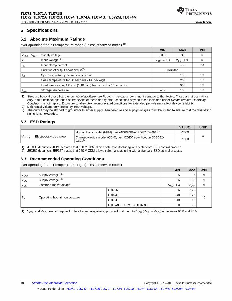
(1) Stresses beyond those listed under Absolute Maximum Ratings may cause permanent damage to the device. These are stress ratingsonly, and functional operation of the device at these or any other conditions beyond those indicated under Recommended OperatingConditions is not implied. Exposure to absolute-maximum-rated conditions for extended periods may affect device reliability.
(2) Differential voltage only limited by input voltage.(3) The output may be shorted to ground or to either supply. Temperature and supply voltages must be limited to ensure that the dissipation
rating is not exceeded.
6 Specifications
6.1 Absolute Maximum Ratingsover operating free-air temperature range (unless otherwise noted) (1)
MIN MAX UNITVCC+ - VCC– Supply voltage –0.3 36 VVI Input voltage (2) VCC– – 0.3 VCC– + 36 VIIK Input clamp current –50 mA
Duration of output short circuit (3) UnlimitedTJ Operating virtual junction temperature 150 °C
Case temperature for 60 seconds - FK package 260 °CLead temperature 1.8 mm (1/16 inch) from case for 10 seconds 300 °C
Tstg Storage temperature –65 150 °C
(1) JEDEC document JEP155 states that 500-V HBM allows safe manufacturing with a standard ESD control process.(2) JEDEC document JEP157 states that 250-V CDM allows safe manufacturing with a standard ESD control process.
6.2 ESD RatingsVALUE UNIT
V(ESD) Electrostatic dischargeHuman body model (HBM), per ANSI/ESDA/JEDEC JS-001 (1) ±2000
VCharged-device model (CDM), per JEDEC specification JESD22-C101 (2) ±1000
(1) VCC+ and VCC– are not required to be of equal magnitude, provided that the total VCC (VCC+ – VCC–) is between 10 V and 30 V.
6.3 Recommended Operating Conditionsover operating free-air temperature range (unless otherwise noted)
MIN MAX UNITVCC+ Supply voltage (1) 5 15 VVCC– Supply voltage (1) –5 –15 VVCM Common-mode voltage VCC– + 4 VCC+ V
TA Operating free-air temperature
TL07xM –55 125
°CTL08xQ –40 125TL07xI –40 85TL07xAC, TL07xBC, TL07xC 0 70

11
TL071, TL071A, TL071BTL072, TL072A, TL072B, TL074, TL074A, TL074B, TL072M, TL074M
www.ti.com SLOS080N –SEPTEMBER 1978–REVISED JULY 2017
Product Folder Links: TL071 TL071A TL071B TL072 TL072A TL072B TL074 TL074A TL074B TL072M TL074M
Submit Documentation FeedbackCopyright © 1978–2017, Texas Instruments Incorporated
(1) For more information about traditional and new thermal metrics, see the Semiconductor and IC Package Thermal Metrics applicationreport.
6.4 Thermal Information: TL071x
THERMAL METRIC (1)TL071x
UNITD (SOIC) P (PDIP) PS (SO)8 PINS 8 PINS 8 PINS
RθJA Junction-to-ambient thermal resistance 97 85 95 °C/WRθJC(top) Junction-to-case (top) thermal resistance — — — °C/W
(1) For more information about traditional and new thermal metrics, see the Semiconductor and IC Package Thermal Metrics applicationreport.
6.5 Thermal Information: TL072x
THERMAL METRIC (1)TL072x
UNITD (SOIC) JG (CDIP) P (PDIP) PS (SO)8 PINS 8 PINS 8 PINS 8 PINS
RθJA Junction-to-ambient thermal resistance 97 — 85 95 °C/WRθJC(top) Junction-to-case (top) thermal resistance — 15.05 — — °C/W
(1) For more information about traditional and new thermal metrics, see the Semiconductor and IC Package Thermal Metrics applicationreport.
6.6 Thermal Information: TL072x (cont.)
THERMAL METRIC (1)TL072x
UNITPW (TSSOP) U (CFP) FK (LCCC)8 PINS 10 PINS 20 PINS
RθJA Junction-to-ambient thermal resistance 150 169.8 — °C/WRθJC(top) Junction-to-case (top) thermal resistance — 62.1 5.61 °C/WRθJB Junction-to-board thermal resistance — 176.2 — °C/WψJT Junction-to-top characterization parameter — 48.4 — °C/WψJB Junction-to-board characterization parameter — 144.1 — °C/WRθJC(bot) Junction-to-case (bottom) thermal resistance — 5.4 — °C/W
(1) For more information about traditional and new thermal metrics, see the Semiconductor and IC Package Thermal Metrics applicationreport.
6.7 Thermal Information: TL074x
THERMAL METRIC (1)TL074x
UNITD (SOIC) N (PDIP) NS (SO)14 PINS 14 PINS 14 PINS
RθJA Junction-to-ambient thermal resistance 86 80 76 °C/WRθJC(top) Junction-to-case (top) thermal resistance — — — °C/W

12
TL071, TL071A, TL071BTL072, TL072A, TL072B, TL074, TL074A, TL074B, TL072M, TL074MSLOS080N –SEPTEMBER 1978–REVISED JULY 2017 www.ti.com
Product Folder Links: TL071 TL071A TL071B TL072 TL072A TL072B TL074 TL074A TL074B TL072M TL074M
Submit Documentation Feedback Copyright © 1978–2017, Texas Instruments Incorporated
(1) For more information about traditional and new thermal metrics, see the Semiconductor and IC Package Thermal Metrics applicationreport.
6.8 Thermal Information: TL074x (cont).
THERMAL METRIC (1)TL074x
UNITJ (CDIP) PW (TSSOP) W (CFP)14 PINS 14 PINS 14 PINS
RθJA Junction-to-ambient thermal resistance — 113 128.8 °C/WRθJC(top) Junction-to-case (top) thermal resistance 14.5 — 56.1 °C/WRθJB Junction-to-board thermal resistance — — 127.6 °C/WψJT Junction-to-top characterization parameter — — 29 °C/WψJB Junction-to-board characterization parameter — — 106.1 °C/WRθJC(bot) Junction-to-case (bottom) thermal resistance — — 0.5 °C/W
(1) For more information about traditional and new thermal metrics, see the Semiconductor and IC Package Thermal Metrics applicationreport.
6.9 Thermal Information: TL074x (cont).
THERMAL METRIC (1)TL074x
UNITFK (LCCC)20 PINS
RθJA Junction-to-ambient thermal resistance — °C/WRθJC(top) Junction-to-case (top) thermal resistance 5.61 °C/W

13
TL071, TL071A, TL071BTL072, TL072A, TL072B, TL074, TL074A, TL074B, TL072M, TL074M
www.ti.com SLOS080N –SEPTEMBER 1978–REVISED JULY 2017
Product Folder Links: TL071 TL071A TL071B TL072 TL072A TL072B TL074 TL074A TL074B TL072M TL074M
Submit Documentation FeedbackCopyright © 1978–2017, Texas Instruments Incorporated
(1) All characteristics are measured under open-loop conditions with zero common-mode voltage, unless otherwise specified.(2) Full range is TA = 0°C to 70°C.(3) Input bias currents of an FET-input operational amplifier are normal junction reverse currents, which are temperature sensitive, as
shown in Figure 1. Pulse techniques must be used that maintain the junction temperature as close to the ambient temperature aspossible.
6.10 Electrical Characteristics: TL071C, TL072C, TL074CVCC± = ±15 V (unless otherwise noted)
PARAMETER TEST CONDITIONS (1) (2) MIN TYP MAX UNIT
VIO Input offset voltage VO = 0RS = 50 Ω
TA = 25°C 3 10mV
TA = Full range 13
α Temperature coefficient ofinput offset voltage
VO = 0RS = 50 Ω TA = Full range 18 µV/°C
IIO Input offset current VO = 0TA = 25°C 5 100 pATA = Full range 10 nA
IIB Input bias current (3) VO = 0TA = 25°C 65 200 pATA = Full range 7 nA
VICRCommon-mode input voltagerange TA = 25°C ±11 –12 to 15 V
VOMMaximum peak outputvoltage swing
RL= 10 kΩ TA = 25°C ±12 ±13.5VRL≥ 10 kΩ
TA = Full range±12
RL≥ 2 kΩ ±10
AVDLarge-signal differentialvoltage amplification
VO = ±10 VRL≥ 2 kΩ
TA = 25°C 25 200V/mV
TA = Full range 15B1 Utility-gain bandwidth TA = 25°C 3 MHzrI Input resistance TA = 25°C 1012 Ω
CMRR Common-mode rejectionratio
VIC = VICR(min)VO = 0RS = 50 Ω
TA = 25°C 70 100 dB
kSVRSupply voltage rejection ratio(ΔVCC±/ΔVIO)
VCC = ±9 V to ±15 VVO = 0RS = 50 Ω
TA = 25°C 70 100 dB
ICCSupply current (eachamplifier) VO = 0; no load TA = 25°C 1.4 2.5 mA
VO1 / VO2 Crosstalk attenuation AVD = 100 TA = 25°C 120 dB

14
TL071, TL071A, TL071BTL072, TL072A, TL072B, TL074, TL074A, TL074B, TL072M, TL074MSLOS080N –SEPTEMBER 1978–REVISED JULY 2017 www.ti.com
Product Folder Links: TL071 TL071A TL071B TL072 TL072A TL072B TL074 TL074A TL074B TL072M TL074M
Submit Documentation Feedback Copyright © 1978–2017, Texas Instruments Incorporated
(1) All characteristics are measured under open-loop conditions with zero common-mode voltage, unless otherwise specified.(2) Full range is TA = 0°C to 70°C.(3) Input bias currents of an FET-input operational amplifier are normal junction reverse currents, which are temperature sensitive, as
shown in Figure 1. Pulse techniques must be used that maintain the junction temperature as close to the ambient temperature aspossible.
6.11 Electrical Characteristics: TL071AC, TL072AC, TL074ACVCC± = ±15 V (unless otherwise noted)
PARAMETER TEST CONDITIONS (1) (2) MIN TYP MAX UNIT
VIO Input offset voltage VO = 0RS = 50 Ω
TA = 25°C 3 6mV
TA = Full range 7.5
α Temperature coefficient ofinput offset voltage
VO = 0RS = 50 Ω TA = Full range 18 µV/°C
IIO Input offset current VO = 0TA = 25°C 5 100 pATA = Full range 2 nA
IIB Input bias current (3) VO = 0TA = 25°C 65 200 pATA = Full range 7 nA
VICRCommon-mode input voltagerange TA = 25°C ±11 –12 to 15 V
VOMMaximum peak outputvoltage swing
RL= 10 kΩ TA = 25°C ±12 ±13.5VRL≥ 10 kΩ
TA = Full range±12
RL≥ 2 kΩ ±10
AVDLarge-signal differentialvoltage amplification
VO = ±10 VRL≥ 2 kΩ
TA = 25°C 50 200V/mV
TA = Full range 25B1 Utility-gain bandwidth TA = 25°C 3 MHzrI Input resistance TA = 25°C 1012 Ω
CMRR Common-mode rejection ratioVIC = VICR(min)VO = 0RS = 50 Ω
TA = 25°C 75 100 dB
kSVRSupply-voltage rejection ratio(ΔVCC± / ΔVIO)
VCC = ±9 V to ±15 VVO = 0RS = 50 Ω
TA = 25°C 80 100 dB
ICCSupply current(each amplifier) VO = 0; no load TA = 25°C 1.4 2.5 mA
VO1 / VO2 Crosstalk attenuation AVD = 100 TA = 25°C 120 dB

15
TL071, TL071A, TL071BTL072, TL072A, TL072B, TL074, TL074A, TL074B, TL072M, TL074M
www.ti.com SLOS080N –SEPTEMBER 1978–REVISED JULY 2017
Product Folder Links: TL071 TL071A TL071B TL072 TL072A TL072B TL074 TL074A TL074B TL072M TL074M
Submit Documentation FeedbackCopyright © 1978–2017, Texas Instruments Incorporated
(1) All characteristics are measured under open-loop conditions with zero common-mode voltage, unless otherwise specified.(2) Full range is TA = 0°C to 70°C.(3) Input bias currents of an FET-input operational amplifier are normal junction reverse currents, which are temperature sensitive, as
shown in Figure 1. Pulse techniques must be used that maintain the junction temperature as close to the ambient temperature aspossible.
6.12 Electrical Characteristics: TL071BC, TL072BC, TL074BCVCC± = ±15 V (unless otherwise noted)
PARAMETER TEST CONDITIONS (1) (2) MIN TYP MAX UNIT
VIO Input offset voltage VO = 0RS = 50 Ω
TA = 25°C 2 3mV
TA = Full range 5
α Temperature coefficient ofinput offset voltage
VO = 0RS = 50 Ω TA = Full range 18 µV/°C
IIO Input offset current VO = 0TA = 25°C 5 100 pATA = Full range 2 nA
IIB Input bias current (3) VO = 0TA = 25°C 65 200 pATA = Full range 7 nA
VICRCommon-mode inputvoltage range TA = 25°C ±11 –12 to 15 V
VOMMaximum peak outputvoltage swing
RL= 10 kΩ TA = 25°C ±12 ±13.5VRL≥ 10 kΩ
TA = Full range±12
RL≥ 2 kΩ ±10
AVDLarge-signal differentialvoltage amplification
VO = ±10 VRL ≥ 2 kΩ
TA = 25°C 50 200V/mV
TA = Full range 25B1 Utility-gain bandwidth TA = 25°C 3 MHzrI Input resistance TA = 25°C 1012 Ω
CMRR Common-mode rejectionratio
VIC = VICR(min)VO = 0RS = 50 Ω
TA = 25°C 75 100 dB
kSVRSupply-voltage rejectionratio (ΔVCC±/ΔVIO)
VCC = ±9 V to ±15 VVO = 0RS = 50 Ω
TA = 25°C 80 100 dB
ICCSupply current (eachamplifier) VO = 0; no load TA = 25°C 1.4 2.5 mA
VO1 / VO2 Crosstalk attenuation AVD = 100 TA = 25°C 120 dB

16
TL071, TL071A, TL071BTL072, TL072A, TL072B, TL074, TL074A, TL074B, TL072M, TL074MSLOS080N –SEPTEMBER 1978–REVISED JULY 2017 www.ti.com
Product Folder Links: TL071 TL071A TL071B TL072 TL072A TL072B TL074 TL074A TL074B TL072M TL074M
Submit Documentation Feedback Copyright © 1978–2017, Texas Instruments Incorporated
(1) All characteristics are measured under open-loop conditions with zero common-mode voltage, unless otherwise specified.(2) TA = –40°C to 85°C.(3) Input bias currents of an FET-input operational amplifier are normal junction reverse currents, which are temperature sensitive, as
shown in Figure 1. Pulse techniques must be used that maintain the junction temperature as close to the ambient temperature aspossible.
6.13 Electrical Characteristics: TL071I, TL072I, TL074IVCC± = ±15 V (unless otherwise noted)
PARAMETER TEST CONDITIONS (1) (2) MIN TYP MAX UNIT
VIO Input offset voltage VO = 0RS = 50 Ω
TA = 25°C 3 6mV
TA = Full range 8
α Temperature coefficient ofinput offset voltage
VO = 0RS = 50 Ω TA = Full range 18 µV/°C
IIO Input offset current VO = 0TA = 25°C 5 100 pATA = Full range 2 nA
IIB Input bias current (3) VO = 0TA = 25°C 65 200 pATA = Full range 7 nA
VICRCommon-mode input voltagerange TA = 25°C ±11 –12 to 15 V
VOMMaximum peak outputvoltage swing
RL= 10 kΩ TA = 25°C ±12 ±13.5VRL ≥ 10 kΩ
TA = Full range±12
RL ≥ 2 kΩ ±10
AVDLarge-signal differentialvoltage amplification
VO = ±10 VRL ≥ 2 kΩ
TA = 25°C 50 200V/mV
TA = Full range 25B1 Utility-gain bandwidth TA = 25°C 3 MHzrI Input resistance TA = 25°C 1012 Ω
CMRR Common-mode rejectionratio
VIC = VICR(min)VO = 0RS = 50 Ω
TA = 25°C 75 100 dB
kSVRSupply-voltage rejection ratio(ΔVCC±/ΔVIO)
VCC = ±9 V to ±15 VVO = 0RS = 50 Ω
TA = 25°C 80 100 dB
ICCSupply current (eachamplifier) VO = 0; no load TA = 25°C 1.4 2.5 mA
VO1 / VO2 Crosstalk attenuation AVD = 100 TA = 25°C 120 dB

17
TL071, TL071A, TL071BTL072, TL072A, TL072B, TL074, TL074A, TL074B, TL072M, TL074M
www.ti.com SLOS080N –SEPTEMBER 1978–REVISED JULY 2017
Product Folder Links: TL071 TL071A TL071B TL072 TL072A TL072B TL074 TL074A TL074B TL072M TL074M
Submit Documentation FeedbackCopyright © 1978–2017, Texas Instruments Incorporated
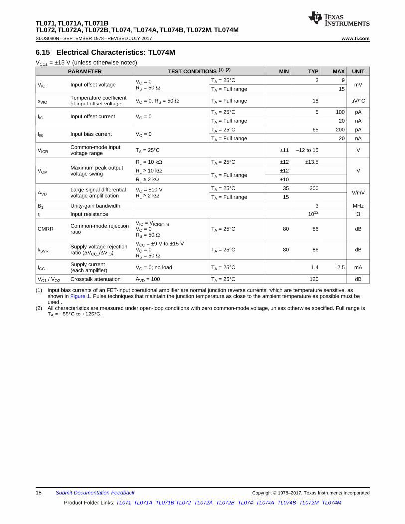
(1) Input bias currents of an FET-input operational amplifier are normal junction reverse currents, which are temperature sensitive, asshown in Figure 1. Pulse techniques that maintain the junction temperature as close to the ambient temperature as possible must beused.
(2) All characteristics are measured under open-loop conditions with zero common-mode voltage, unless otherwise specified. Full range isTA = –55°C to +125°C.
6.14 Electrical Characteristics: TL071M, TL072MVCC± = ±15 V (unless otherwise noted)
PARAMETER TEST CONDITIONS (1) (2) MIN TYP MAX UNIT
VIO Input offset voltage VO = 0RS = 50 Ω
TA = 25°C 3 6mV
TA = Full range 9
αVIOTemperature coefficientof input offset voltage
VO = 0RS = 50 Ω TA = Full range 18 μV/°C
IIO Input offset current VO = 0TA = 25°C 5 100 pATA = Full range 20 nA
IIB Input bias current VO = 0TA = 25°C 65 200 pATA = Full range 50 nA
VICRCommon-mode inputvoltage range TA = 25°C ±11 –12 to 15 V
VOMMaximum peak outputvoltage swing
RL = 10 kΩ TA = 25°C ±12 ±13.5VRL ≥ 10 kΩ
TA = Full range±12
RL ≥ 2 kΩ ±10
AVDLarge-signal differentialvoltage amplification
VO = ±10 VRL ≥ 2 kΩ
TA = 25°C 35 200V/mV
TA = Full range 15B1 Unity-gain bandwidth 3 MHzri Input resistance 1012 Ω
CMRR Common-mode rejectionratio
VIC = VICR(min),VO = 0RS = 50 Ω
TA = 25°C 80 86 dB
kSVRSupply-voltage rejectionratio (ΔVCC±/ΔVIO)
VCC = ±9 V to ±15 VVO = 0RS = 50 Ω
TA = 25°C 80 86 dB
ICCSupply current(each amplifier) VO = 0; no load TA = 25°C 1.4 2.5 mA
VO1 / VO2 Crosstalk attenuation AVD = 100 TA = 25°C 120 dB
18
TL071, TL071A, TL071BTL072, TL072A, TL072B, TL074, TL074A, TL074B, TL072M, TL074MSLOS080N –SEPTEMBER 1978–REVISED JULY 2017 www.ti.com
Product Folder Links: TL071 TL071A TL071B TL072 TL072A TL072B TL074 TL074A TL074B TL072M TL074M
Submit Documentation Feedback Copyright © 1978–2017, Texas Instruments Incorporated
(1) Input bias currents of an FET-input operational amplifier are normal junction reverse currents, which are temperature sensitive, asshown in Figure 1. Pulse techniques that maintain the junction temperature as close to the ambient temperature as possible must beused .
(2) All characteristics are measured under open-loop conditions with zero common-mode voltage, unless otherwise specified. Full range isTA = –55°C to +125°C.
6.15 Electrical Characteristics: TL074MVCC± = ±15 V (unless otherwise noted)
PARAMETER TEST CONDITIONS (1) (2) MIN TYP MAX UNIT
VIO Input offset voltage VO = 0RS = 50 Ω
TA = 25°C 3 9mV
TA = Full range 15
αVIOTemperature coefficientof input offset voltage VO = 0, RS = 50 Ω TA = Full range 18 μV/°C
IIO Input offset current VO = 0TA = 25°C 5 100 pATA = Full range 20 nA
IIB Input bias current VO = 0TA = 25°C 65 200 pATA = Full range 20 nA
VICRCommon-mode inputvoltage range TA = 25°C ±11 –12 to 15 V
VOMMaximum peak outputvoltage swing
RL = 10 kΩ TA = 25°C ±12 ±13.5VRL ≥ 10 kΩ
TA = Full range±12
RL ≥ 2 kΩ ±10
AVDLarge-signal differentialvoltage amplification
VO = ±10 VRL ≥ 2 kΩ
TA = 25°C 35 200V/mV
TA = Full range 15B1 Unity-gain bandwidth 3 MHzri Input resistance 1012 Ω
CMRR Common-mode rejectionratio
VIC = VICR(min)VO = 0RS = 50 Ω
TA = 25°C 80 86 dB
kSVRSupply-voltage rejectionratio (ΔVCC±/ΔVIO)
VCC = ±9 V to ±15 VVO = 0RS = 50 Ω
TA = 25°C 80 86 dB
ICCSupply current(each amplifier) VO = 0; no load TA = 25°C 1.4 2.5 mA
VO1 / VO2 Crosstalk attenuation AVD = 100 TA = 25°C 120 dB

19
TL071, TL071A, TL071BTL072, TL072A, TL072B, TL074, TL074A, TL074B, TL072M, TL074M
www.ti.com SLOS080N –SEPTEMBER 1978–REVISED JULY 2017
Product Folder Links: TL071 TL071A TL071B TL072 TL072A TL072B TL074 TL074A TL074B TL072M TL074M
Submit Documentation FeedbackCopyright © 1978–2017, Texas Instruments Incorporated
6.16 Switching Characteristics: TL07xMVCC± = ±15 V, TA = 25°C
PARAMETER TEST CONDITIONS MIN TYP MAX UNIT
SR Slew rate at unity gain VI = 10 VCL = 100 pF
RL = 2 kΩSee Figure 21 5 13 V/μs
tr Rise-time overshoot factor VI = 20 VCL = 100 pF
RL = 2 kΩSee Figure 21
0.1 μs20%
VnEquivalent input noisevoltage RS = 20 Ω
f = 1 kHz 18 nV/√Hzf = 10 Hz to 10 kHz 4 μV
In Equivalent input noise current RS = 20 Ω f = 1 kHz 0.01 pA/√Hz
THD Total harmonic distortionVIrms = 6 VRL ≥ 2 kΩf = 1 kHz
AVD = 1RS ≤ 1 kΩ 0.003%
6.17 Switching Characteristics: TL07xC, TL07xAC, TL07xBC, TL07xIVCC± = ±15 V, TA = 25°C
PARAMETER TEST CONDITIONS MIN TYP MAX UNIT
SR Slew rate at unity gain VI = 10 VCL = 100 pF
RL = 2 kΩSee Figure 21 8 13 V/μs
tr Rise-time overshoot factor VI = 20 VCL = 100 pF
RL = 2 kΩSee Figure 21
0.1 μs20%
VnEquivalent input noisevoltage RS = 20 Ω
f = 1 kHz 18 nV/√Hzf = 10 Hz to 10 kHz 4 μV
In Equivalent input noise current RS = 20 Ω f = 1 kHz 0.01 pA/√Hz
THD Total harmonic distortionVIrms = 6 VRL ≥ 2 kΩf = 1 kHz
AVD = 1RS ≤ 1 kΩ 0.003%

20
TL071, TL071A, TL071BTL072, TL072A, TL072B, TL074, TL074A, TL074B, TL072M, TL074MSLOS080N –SEPTEMBER 1978–REVISED JULY 2017 www.ti.com
Product Folder Links: TL071 TL071A TL071B TL072 TL072A TL072B TL074 TL074A TL074B TL072M TL074M
Submit Documentation Feedback Copyright © 1978–2017, Texas Instruments Incorporated
6.18 Typical CharacteristicsData at high and low temperatures are applicable only within the rated operating free-air temperature ranges of the variousdevices.
Table 1. Typical Characteristics: Table of GraphsFIGURE
IIB Input bias current versus free-air temperature Figure 1
VOM Maximum peak output voltage
versus frequencyFigure 2Figure 3Figure 4
versus free-air temperature Figure 5versus load resistance Figure 6versus supply voltage Figure 7
AVDLarge signal differential voltageamplification
versus free-air temperature Figure 8versus load resistance Figure 9
Phase shift versus frequency Figure 9Normalized unity-gain bandwidth versus free-air temperature Figure 10Normalized phase shift versus free-air temperature Figure 10
CMRR Common-mode rejection ratio versus free-air temperature Figure 11Input offset voltage change versus common-mode voltage Figure 20
ICC Supply currentversus free-air temperature Figure 13versus supply voltage Figure 12
PD Total power dissipation versus free-air temperature Figure 14Normalized slew rate versus free-air temperature Figure 15
Vn Equivalent input noise voltage versus frequency Figure 16THD Total harmonic distortion versus frequency Figure 17
Large-signal pulse response versus time Figure 18VO Output voltage versus elapsed time Figure 19

−750
VO
M−
Maxim
um
Peak O
utp
ut
Vo
ltag
e−
V
TA − Free-Air Temperature − °C
125
±15
−50 −25 0 25 50 75 100
±2.5
±5
±7.5
±10
±12.5
RL = 10 kΩ
VCC± = ±15 V
See Figure 2
VO
M
RL = 2 kΩ
8
0.10
RL − Load Resistance − kΩ
10
±15
±2.5
±5
±7.5
±10
±12.5
VCC± = ±15 V
TA = 25°C
See Figure 2
0.2 0.4 0.7 1 2 4 7
VO
M−
Maxim
um
Peak
Ou
tpu
t Vo
ltag
e−
VVO
M
8
10 M1 M100 k10 k1 k100
f − Frequency − Hz
VO
M−
Maxim
um
Peak
Ou
tpu
t Vo
ltag
e−
V
0
±2.5
±5
±7.5
±10
±12.5
±15
See Figure 2
TA = 25°C
RL = 2 kΩ
VCC± = ±10 V
VCC± = ±5 V
VO
M
VCC± = ±15 V
8
RL = 10 kΩ
TA = 25°C
See Figure 2
±15
±12.5
±10
±7.5
±5
±2.5
0
VO
M−
Maxim
um
Peak O
utp
ut
Vo
ltag
e−
V
f − Frequency − Hz
100 1 k 10 k 100 k 1 M 10 M
VO
M
VCC± = ±5 V
VCC± = ±10 V
VCC± = ±15 V
IIB
−In
pu
t B
ias C
urr
en
t−
nA
TA − Free-Air Temperature − °C
IBI
10
1
0.1
0.01
100
−75 −50 −25 0 25 50 75 100 125
VCC± = ±15 V
21
TL071, TL071A, TL071BTL072, TL072A, TL072B, TL074, TL074A, TL074B, TL072M, TL074M
www.ti.com SLOS080N –SEPTEMBER 1978–REVISED JULY 2017
Product Folder Links: TL071 TL071A TL071B TL072 TL072A TL072B TL074 TL074A TL074B TL072M TL074M
Submit Documentation FeedbackCopyright © 1978–2017, Texas Instruments Incorporated
6.18.1 Typical Characteristics
Figure 1. Input Bias Current vs Free-Air Temperature Figure 2. Maximum Peak Output Voltage vs Frequency
Figure 3. Maximum Peak Output Voltage vs Frequency Figure 4. Maximum Peak Output Voltage vs Frequency
Figure 5. Maximum Peak Output Voltage vs Free-AirTemperature
Figure 6. Maximum Peak Output Voltage vs LoadResistance

−7583
CM
RR
−C
om
mo
n-M
od
e R
eje
cti
on
Rati
o−
dB
TA − Free-Air Temperature − °C
125
89
−50 −25 0 25 50 75 100
84
85
86
87
88
VCC± = ±15 V
RL = 10 kΩ
00
|VCC±| − Supply Voltage − V
16
2
2 4 6 8 10 12 14
0.2
0.4
0.6
0.8
1
1.2
1.4
1.6
1.8TA = 25°C
No SignalNo Load
ICC
−S
up
ply
Cu
rren
t P
erA
mp
lifi
er
−m
AC
C±
I
1.02
1.01
1
0.99
0.98
1.03
0.97
−750.7
No
rmalized
Un
ity-G
ain
Ban
dw
idth
TA − Free-Air Temperature − °C
125
1.3
−50 −25 0 25 50 75 100
0.8
0.9
1
1.1
1.2 Unity-Gain Bandwidth
VCC± = ±15 V
RL = 2 kΩ
f = B1 for Phase Shift
Phase Shift
No
rmalized
Ph
ase
Sh
ift
00
VO
M−
Maxim
um
Peak O
utp
ut
Vo
ltag
e−
V
|VCC±| − Supply Voltage − V
16
±15
2 4 6 8 10 12 14
±2.5
±5
±7.5
±10
±12.5
RL = 10 kΩ
TA = 25°C
VO
M
−751
Vo
ltag
eA
mp
lifi
cati
on
−V
/mV
TA − Free-Air Temperature − °C
125
1000
−50 −25 0 25 50 75 100
2
4
10
20
40
100
200
400
VCC± = ±15 V
VO = ±10 VRL = 2 kΩ
AV
D−
Larg
e-S
ign
al D
iffe
ren
tial
AV
D
22
TL071, TL071A, TL071BTL072, TL072A, TL072B, TL074, TL074A, TL074B, TL072M, TL074MSLOS080N –SEPTEMBER 1978–REVISED JULY 2017 www.ti.com
Product Folder Links: TL071 TL071A TL071B TL072 TL072A TL072B TL074 TL074A TL074B TL072M TL074M
Submit Documentation Feedback Copyright © 1978–2017, Texas Instruments Incorporated
Typical Characteristics (continued)
Figure 7. Maximum Peak Output Voltage vs SupplyVoltage
Figure 8. Large-Signal Differential Voltage Amplification vsFree-Air Temperature
Figure 9. Large-Signal Differential Voltage Amplificationand Phase Shift vs Frequency
Figure 10. Normalized Unity-Gain Bandwidth and PhaseShift vs Free-Air Temperature
Figure 11. Common-Mode Rejection Ratio vs Free-AirTemperature
Figure 12. Supply Current Per Amplifier vs Supply Voltage
−6
t − Time − µs
3.5
6
0 0.5 1 1.5 2 2.5 3
−4
−2
0
2
4
Output
Input
VCC± = ±15 V
RL = 2 kΩ
TA = 25°C
CL = 100 pF
VO
VI
−In
pu
t an
d O
utp
ut
Vo
ltag
es
−V
an
d
0.001
TH
D−
To
tal
Harm
on
ic D
isto
rtio
n−
%
1
40 k10 k4 k1 k400 100 k
f − Frequency − Hz
100
0.004
0.01
0.04
0.1
0.4
VCC± = ±15 V
AVD = 1
VI(RMS) = 6 V
TA = 25°C
100
−E
qu
ivale
nt
Inp
ut
No
ise
Vo
ltag
e−
nV
/Hz
f − Frequency − Hz
100 k
50
10
20
30
40
VCC± = ±15 V
AVD = 10
RS = 20 Ω
TA = 25°C
40 100 400 1 k 4 k 10 k 40 k
nV
/H
zV
n
−750
TA − Free-Air Temperature − °C
125
2
−50 −25 0 25 50 75 100
0.2
0.4
0.6
0.8
1
1.2
1.4
1.6
1.8
VCC± = ±15 V
No Signal
No Load
ICC
−S
up
ply
Cu
rren
t P
erA
mp
lifi
er
−m
AC
C±
I
−750
TA − Free-Air Temperature −C°
125
250
−50 −25 0 25 50 75 100
25
50
75
100
125
150
175
200
225VCC± = 15 V±
No SignalNo Load
TL074
TL071
TL072
−To
tal
Po
wer
Dis
sip
ati
on
−m
WP
D
23
TL071, TL071A, TL071BTL072, TL072A, TL072B, TL074, TL074A, TL074B, TL072M, TL074M
www.ti.com SLOS080N –SEPTEMBER 1978–REVISED JULY 2017
Product Folder Links: TL071 TL071A TL071B TL072 TL072A TL072B TL074 TL074A TL074B TL072M TL074M
Submit Documentation FeedbackCopyright © 1978–2017, Texas Instruments Incorporated
Typical Characteristics (continued)
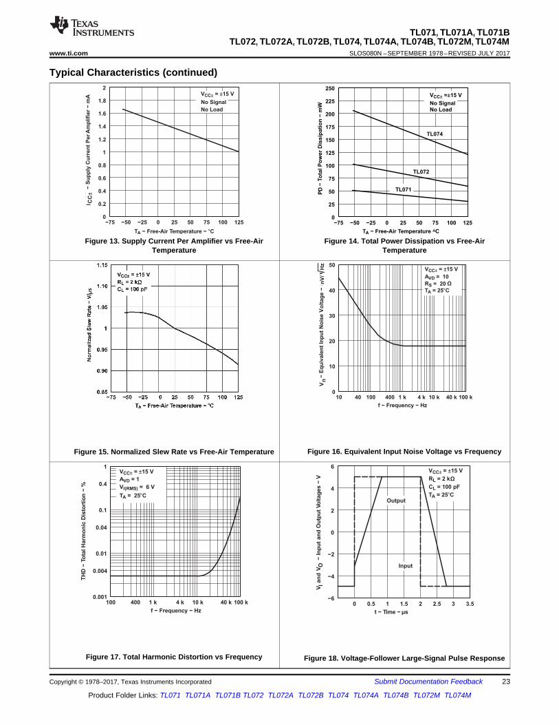
Figure 13. Supply Current Per Amplifier vs Free-AirTemperature
Figure 14. Total Power Dissipation vs Free-AirTemperature
Figure 15. Normalized Slew Rate vs Free-Air Temperature Figure 16. Equivalent Input Noise Voltage vs Frequency
Figure 17. Total Harmonic Distortion vs Frequency Figure 18. Voltage-Follower Large-Signal Pulse Response

VCM (V)
VIO
(m
V)
-13 -11 -9 -7 -5 -3 -1 1 3 5 7 9 11 13 15 17-10
-8
-6
-4
-2
0
2
4
6
8
10
D003
VCCr = r15 V
24
TL071, TL071A, TL071BTL072, TL072A, TL072B, TL074, TL074A, TL074B, TL072M, TL074MSLOS080N –SEPTEMBER 1978–REVISED JULY 2017 www.ti.com
Product Folder Links: TL071 TL071A TL071B TL072 TL072A TL072B TL074 TL074A TL074B TL072M TL074M
Submit Documentation Feedback Copyright © 1978–2017, Texas Instruments Incorporated
Typical Characteristics (continued)
Figure 19. Output Voltage vs Elapsed Time Figure 20. VIO vs VCM

VI
10 kΩ
1 kΩ
RL CL = 100 pF
+
−
OUT
VI
CL = 100 pF RL = 2 kΩ
+
−
OUT
25
TL071, TL071A, TL071BTL072, TL072A, TL072B, TL074, TL074A, TL074B, TL072M, TL074M
www.ti.com SLOS080N –SEPTEMBER 1978–REVISED JULY 2017
Product Folder Links: TL071 TL071A TL071B TL072 TL072A TL072B TL074 TL074A TL074B TL072M TL074M
Submit Documentation FeedbackCopyright © 1978–2017, Texas Instruments Incorporated
6.1 Parameter Measurement Information
Figure 21. Unity-Gain Amplifier
Figure 22. Gain-of-10 Inverting Amplifier
Figure 23. Input Offset-Voltage Null Circuit

C1
VCC+
IN+
VCC−
1080 Ω 1080 Ω
IN−
TL071 Only
64 Ω128 Ω
64 Ω
All component values shown are nominal.
OFFSET
N1
OFFSET
N2
OUT
18 pF
COMPONENT COUNT†
COMPONENT
TYPETL071 TL072 TL074
Resistors 11 22 44Resistors
Transistors
11
14
22
28
44
56Transistors
JFET
14
2
28
4
56
6JFET
Diodes
2
1
4
2
6
4Diodes
Capacitors
1
1
2
2
4
4Capacitors
epi-FET
1
1
2
2
4
4
† Includes bias and trim circuitry
26
TL071, TL071A, TL071BTL072, TL072A, TL072B, TL074, TL074A, TL074B, TL072M, TL074MSLOS080N –SEPTEMBER 1978–REVISED JULY 2017 www.ti.com
Product Folder Links: TL071 TL071A TL071B TL072 TL072A TL072B TL074 TL074A TL074B TL072M TL074M
Submit Documentation Feedback Copyright © 1978–2017, Texas Instruments Incorporated
7 Detailed Description
7.1 OverviewThe JFET-input operational amplifiers in the TL07xx series are similar to the TL08x series, with low input biasand offset currents, and a fast slew rate. The low harmonic distortion and low noise make the TL07xx seriesideally suited for high-fidelity and audio preamplifier applications. Each amplifier features JFET inputs (for highinput impedance) coupled with bipolar output stages integrated on a single monolithic chip.
The C-suffix devices are characterized for operation from 0°C to 70°C. The I-suffix devices are characterized foroperation from −40°C to +85°C. The M-suffix devices are characterized for operation over the full militarytemperature range of −55°C to +125°C.
7.2 Functional Block Diagram

27
TL071, TL071A, TL071BTL072, TL072A, TL072B, TL074, TL074A, TL074B, TL072M, TL074M
www.ti.com SLOS080N –SEPTEMBER 1978–REVISED JULY 2017
Product Folder Links: TL071 TL071A TL071B TL072 TL072A TL072B TL074 TL074A TL074B TL072M TL074M
Submit Documentation FeedbackCopyright © 1978–2017, Texas Instruments Incorporated
7.3 Feature Description
7.3.1 Total Harmonic DistortionHarmonic distortions to an audio signal are created by electronic components in a circuit. Total harmonicdistortion (THD) is a measure of harmonic distortions accumulated by a signal in an audio system. These deviceshave a very low THD of 0.003% meaning that the TL07x device adds little harmonic distortion when used inaudio signal applications.
7.3.2 Slew RateThe slew rate is the rate at which an operational amplifier can change the output when there is a change on theinput. These devices have a 13-V/μs slew rate.
7.4 Device Functional ModesThese devices are powered on when the supply is connected. These devices can be operated as a single-supplyoperational amplifier or dual-supply amplifier depending on the application.

V
RFA =
RI-
V
1.8A = 3.6
0.5= -
-
V
VOUTA =
VIN
Vsup+
+VOUT
RF
VIN
RI
Vsup-
Copyright © 2016, Texas Instruments Incorporated
28
TL071, TL071A, TL071BTL072, TL072A, TL072B, TL074, TL074A, TL074B, TL072M, TL074MSLOS080N –SEPTEMBER 1978–REVISED JULY 2017 www.ti.com
Product Folder Links: TL071 TL071A TL071B TL072 TL072A TL072B TL074 TL074A TL074B TL072M TL074M
Submit Documentation Feedback Copyright © 1978–2017, Texas Instruments Incorporated
8 Application and Implementation
NOTEInformation in the following applications sections is not part of the TI componentspecification, and TI does not warrant its accuracy or completeness. TI’s customers areresponsible for determining suitability of components for their purposes. Customers shouldvalidate and test their design implementation to confirm system functionality.
8.1 Application InformationA typical application for an operational amplifier is an inverting amplifier. This amplifier takes a positive voltage onthe input, and makes the voltage a negative voltage. In the same manner, the amplifier makes negative voltagespositive.
8.2 Typical Application
Figure 24. Inverting Amplifier
8.2.1 Design RequirementsThe supply voltage must be selected so the supply voltage is larger than the input voltage range and outputrange. For instance, this application scales a signal of ±0.5 V to ±1.8 V. Setting the supply at ±12 V is sufficientto accommodate this application.
8.2.2 Detailed Design ProcedureDetermine the gain required by the inverting amplifier:
(1)
(2)
Once the desired gain is determined, select a value for RI or RF. Selecting a value in the kilohm range isdesirable because the amplifier circuit uses currents in the milliamp range. This ensures the part does not drawtoo much current. This example uses 10 kΩ for RI which means 36 kΩ is used for RF. This is determined byEquation 3.
(3)

+
±
+
+12
10 k
U1 TL072
VOUT
Copyright © 2017, Texas Instruments Incorporated
VIN
-2
-1.5
-1
-0.5
0
0.5
1
1.5
2
0 0.5 1 1.5 2
Vo
lts
Time (ms)
VIN
VOUT
29
TL071, TL071A, TL071BTL072, TL072A, TL072B, TL074, TL074A, TL074B, TL072M, TL074M
www.ti.com SLOS080N –SEPTEMBER 1978–REVISED JULY 2017
Product Folder Links: TL071 TL071A TL071B TL072 TL072A TL072B TL074 TL074A TL074B TL072M TL074M
Submit Documentation FeedbackCopyright © 1978–2017, Texas Instruments Incorporated
Typical Application (continued)8.2.3 Application Curve
Figure 25. Input and Output Voltages of the Inverting Amplifier
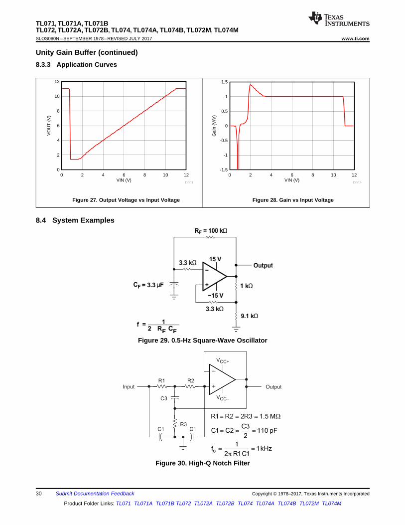
8.3 Unity Gain Buffer
Figure 26. Single-Supply Unity Gain Amplifier
8.3.1 Design Requirements• VCC must be within valid range per Recommended Operating Conditions. This example uses a value of 12 V
for VCC.• Input voltage must be within the recommended common-mode range, as shown in Recommended Operating
Conditions. The valid common-mode range is 4 V to 12 V ( VCC– + 4 V to VCC+.• Output is limited by output range, which is typically 1.5 V to 10.5 V, or VCC– + 1.5 V to VCC+ – 1.5 V.
8.3.2 Detailed Design Procedure• Avoid input voltage values below 1 V to prevent phase reversal where output goes high.• Avoid input values below 4 V to prevent degraded VIO that results in an apparent gain greater than 1. This
may cause instability in some second-order filter designs.
R1Input
R2
C3
C1 C1R3
Output
VCC–
–
+
VCC+
o
R1 R2 2R3 1.5 M
C3C1 C2 110 pF
2
1f 1kHz
2 R1C1
= = = W
= = =
= =p
VIN (V)
VO
UT
(V
)
0 2 4 6 8 10 120
2
4
6
8
10
12
D001VIN (V)
Gai
n (V
/V)
0 2 4 6 8 10 12-1.5
-1
-0.5
0
0.5
1
1.5
D002
30
TL071, TL071A, TL071BTL072, TL072A, TL072B, TL074, TL074A, TL074B, TL072M, TL074MSLOS080N –SEPTEMBER 1978–REVISED JULY 2017 www.ti.com
Product Folder Links: TL071 TL071A TL071B TL072 TL072A TL072B TL074 TL074A TL074B TL072M TL074M
Submit Documentation Feedback Copyright © 1978–2017, Texas Instruments Incorporated
Unity Gain Buffer (continued)8.3.3 Application Curves
Figure 27. Output Voltage vs Input Voltage Figure 28. Gain vs Input Voltage
8.4 System Examples
Figure 29. 0.5-Hz Square-Wave Oscillator
Figure 30. High-Q Notch Filter

31
TL071, TL071A, TL071BTL072, TL072A, TL072B, TL074, TL074A, TL074B, TL072M, TL074M
www.ti.com SLOS080N –SEPTEMBER 1978–REVISED JULY 2017
Product Folder Links: TL071 TL071A TL071B TL072 TL072A TL072B TL074 TL074A TL074B TL072M TL074M
Submit Documentation FeedbackCopyright © 1978–2017, Texas Instruments Incorporated
System Examples (continued)
Figure 31. 100-kHz Quadrature Oscillator
Figure 32. AC Amplifier

32
TL071, TL071A, TL071BTL072, TL072A, TL072B, TL074, TL074A, TL074B, TL072M, TL074MSLOS080N –SEPTEMBER 1978–REVISED JULY 2017 www.ti.com
Product Folder Links: TL071 TL071A TL071B TL072 TL072A TL072B TL074 TL074A TL074B TL072M TL074M
Submit Documentation Feedback Copyright © 1978–2017, Texas Instruments Incorporated
9 Power Supply Recommendations
CAUTIONSupply voltages larger than 36 V for a single-supply or outside the range of ±18 V for adual-supply can permanently damage the device (see the Absolute Maximum Ratings).
Place 0.1-μF bypass capacitors close to the power-supply pins to reduce errors coupling in from noisy or high-impedance power supplies. For more detailed information on bypass capacitor placement, see Layout.
10 Layout
10.1 Layout GuidelinesFor best operational performance of the device, use good PCB layout practices, including:• Noise can propagate into analog circuitry through the power pins of the circuit as a whole, as well as the
operational amplifier. Bypass capacitors are used to reduce the coupled noise by providing low impedancepower sources local to the analog circuitry.– Connect low-ESR, 0.1-μF ceramic bypass capacitors between each supply pin and ground, placed as
close to the device as possible. A single bypass capacitor from V+ to ground is applicable for single-supply applications.
• Separate grounding for analog and digital portions of circuitry is one of the simplest and most-effectivemethods of noise suppression. One or more layers on multilayer PCBs are usually devoted to ground planes.A ground plane helps distribute heat and reduces EMI noise pickup. Take care to physically separate digitaland analog grounds, paying attention to the flow of the ground current. For more detailed information, seeCircuit Board Layout Techniques.
• To reduce parasitic coupling, run the input traces as far away from the supply or output traces as possible. Ifit is not possible to keep them separate, it is much better to cross the sensitive trace perpendicular asopposed to in parallel with the noisy trace.
• Place the external components as close to the device as possible. Keeping RF and RG close to the invertinginput minimizes parasitic capacitance, as shown in Layout Example.
• Keep the length of input traces as short as possible. Always remember that the input traces are the mostsensitive part of the circuit.
• Consider a driven, low-impedance guard ring around the critical traces. A guard ring can significantly reduceleakage currents from nearby traces that are at different potentials.

+RIN
RGRF
VOUTVIN
NC
VCC+IN1í
IN1+
VCCí
NC
OUT
NC
RG
RIN
RF
GND
VIN
VS-GND
VS+
GND
Run the input traces as far away from the supply lines
as possible
Only needed for dual-supply operation
Place components close to device and to each other to
reduce parasitic errors
Use low-ESR, ceramic bypass capacitor
(or GND for single supply) Ground (GND) plane on another layerVOUT
33
TL071, TL071A, TL071BTL072, TL072A, TL072B, TL074, TL074A, TL074B, TL072M, TL074M
www.ti.com SLOS080N –SEPTEMBER 1978–REVISED JULY 2017
Product Folder Links: TL071 TL071A TL071B TL072 TL072A TL072B TL074 TL074A TL074B TL072M TL074M
Submit Documentation FeedbackCopyright © 1978–2017, Texas Instruments Incorporated
10.2 Layout Example
Figure 33. Operational Amplifier Board Layout for Noninverting Configuration
Figure 34. Operational Amplifier Schematic for Noninverting Configuration

34
TL071, TL071A, TL071BTL072, TL072A, TL072B, TL074, TL074A, TL074B, TL072M, TL074MSLOS080N –SEPTEMBER 1978–REVISED JULY 2017 www.ti.com
Product Folder Links: TL071 TL071A TL071B TL072 TL072A TL072B TL074 TL074A TL074B TL072M TL074M
Submit Documentation Feedback Copyright © 1978–2017, Texas Instruments Incorporated
11 Device and Documentation Support
11.1 Documentation Support
11.1.1 Related DocumentationFor related documentation, see the following:
Circuit Board Layout Techniques (SLOA089)
11.2 Related LinksThe table below lists quick access links. Categories include technical documents, support and communityresources, tools and software, and quick access to sample or buy.
Table 2. Related Links
PARTS PRODUCT FOLDER ORDER NOW TECHNICALDOCUMENTS
TOOLS &SOFTWARE
SUPPORT &COMMUNITY
TL071 Click here Click here Click here Click here Click hereTL071A Click here Click here Click here Click here Click hereTL071B Click here Click here Click here Click here Click hereTL072 Click here Click here Click here Click here Click here
TL072A Click here Click here Click here Click here Click hereTL072B Click here Click here Click here Click here Click hereTL072M Click here Click here Click here Click here Click hereTL074 Click here Click here Click here Click here Click here
TL074A Click here Click here Click here Click here Click hereTL074B Click here Click here Click here Click here Click hereTL074M Click here Click here Click here Click here Click here
11.3 Community ResourcesThe following links connect to TI community resources. Linked contents are provided "AS IS" by the respectivecontributors. They do not constitute TI specifications and do not necessarily reflect TI's views; see TI's Terms ofUse.
TI E2E™ Online Community TI's Engineer-to-Engineer (E2E) Community. Created to foster collaborationamong engineers. At e2e.ti.com, you can ask questions, share knowledge, explore ideas and helpsolve problems with fellow engineers.
Design Support TI's Design Support Quickly find helpful E2E forums along with design support tools andcontact information for technical support.
11.4 TrademarksE2E is a trademark of Texas Instruments.All other trademarks are the property of their respective owners.
11.5 Electrostatic Discharge CautionThese devices have limited built-in ESD protection. The leads should be shorted together or the device placed in conductive foamduring storage or handling to prevent electrostatic damage to the MOS gates.
11.6 GlossarySLYZ022 — TI Glossary.
This glossary lists and explains terms, acronyms, and definitions.

35
TL071, TL071A, TL071BTL072, TL072A, TL072B, TL074, TL074A, TL074B, TL072M, TL074M
www.ti.com SLOS080N –SEPTEMBER 1978–REVISED JULY 2017
Product Folder Links: TL071 TL071A TL071B TL072 TL072A TL072B TL074 TL074A TL074B TL072M TL074M
Submit Documentation FeedbackCopyright © 1978–2017, Texas Instruments Incorporated
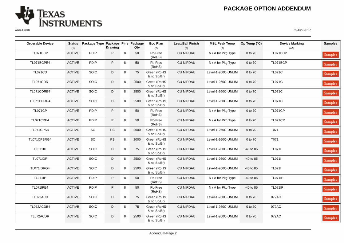
12 Mechanical, Packaging, and Orderable InformationThe following pages include mechanical packaging and orderable information. This information is the mostcurrent data available for the designated devices. This data is subject to change without notice and revision ofthis document. For browser based versions of this data sheet, refer to the left hand navigation.

PACKAGE OPTION ADDENDUM
www.ti.com 2-Jun-2017
Addendum-Page 1
PACKAGING INFORMATION
Orderable Device Status(1)
Package Type PackageDrawing
Pins PackageQty
Eco Plan(2)
Lead/Ball Finish(6)
MSL Peak Temp(3)
Op Temp (°C) Device Marking(4/5)
Samples
81023052A ACTIVE LCCC FK 20 1 TBD POST-PLATE N / A for Pkg Type -55 to 125 81023052ATL072MFKB
8102305HA ACTIVE CFP U 10 1 TBD A42 N / A for Pkg Type -55 to 125 8102305HATL072M
8102305PA ACTIVE CDIP JG 8 1 TBD A42 N / A for Pkg Type -55 to 125 8102305PATL072M
81023062A ACTIVE LCCC FK 20 1 TBD POST-PLATE N / A for Pkg Type -55 to 125 81023062ATL074MFKB
8102306CA ACTIVE CDIP J 14 1 TBD A42 N / A for Pkg Type -55 to 125 8102306CATL074MJB
8102306DA ACTIVE CFP W 14 1 TBD A42 N / A for Pkg Type -55 to 125 8102306DATL074MWB
JM38510/11905BPA ACTIVE CDIP JG 8 1 TBD A42 N / A for Pkg Type -55 to 125 JM38510/11905BPA
M38510/11905BPA ACTIVE CDIP JG 8 1 TBD A42 N / A for Pkg Type -55 to 125 JM38510/11905BPA
TL071ACD ACTIVE SOIC D 8 75 Green (RoHS& no Sb/Br)
CU NIPDAU Level-1-260C-UNLIM 0 to 70 071AC
TL071ACDG4 ACTIVE SOIC D 8 75 Green (RoHS& no Sb/Br)
CU NIPDAU Level-1-260C-UNLIM 0 to 70 071AC
TL071ACDR ACTIVE SOIC D 8 2500 Green (RoHS& no Sb/Br)
CU NIPDAU Level-1-260C-UNLIM 0 to 70 071AC
TL071ACP ACTIVE PDIP P 8 50 Pb-Free(RoHS)
CU NIPDAU N / A for Pkg Type 0 to 70 TL071ACP
TL071ACPE4 ACTIVE PDIP P 8 50 Pb-Free(RoHS)
CU NIPDAU N / A for Pkg Type 0 to 70 TL071ACP
TL071BCD ACTIVE SOIC D 8 75 Green (RoHS& no Sb/Br)
CU NIPDAU Level-1-260C-UNLIM 0 to 70 071BC
TL071BCDE4 ACTIVE SOIC D 8 75 Green (RoHS& no Sb/Br)
CU NIPDAU Level-1-260C-UNLIM 0 to 70 071BC
TL071BCDG4 ACTIVE SOIC D 8 75 Green (RoHS& no Sb/Br)
CU NIPDAU Level-1-260C-UNLIM 0 to 70 071BC
TL071BCDR ACTIVE SOIC D 8 2500 Green (RoHS& no Sb/Br)
CU NIPDAU Level-1-260C-UNLIM 0 to 70 071BC
PACKAGE OPTION ADDENDUM
www.ti.com 2-Jun-2017
Addendum-Page 2
Orderable Device Status(1)
Package Type PackageDrawing
Pins PackageQty
Eco Plan(2)
Lead/Ball Finish(6)
MSL Peak Temp(3)
Op Temp (°C) Device Marking(4/5)
Samples
TL071BCP ACTIVE PDIP P 8 50 Pb-Free(RoHS)
CU NIPDAU N / A for Pkg Type 0 to 70 TL071BCP
TL071BCPE4 ACTIVE PDIP P 8 50 Pb-Free(RoHS)
CU NIPDAU N / A for Pkg Type 0 to 70 TL071BCP
TL071CD ACTIVE SOIC D 8 75 Green (RoHS& no Sb/Br)
CU NIPDAU Level-1-260C-UNLIM 0 to 70 TL071C
TL071CDR ACTIVE SOIC D 8 2500 Green (RoHS& no Sb/Br)
CU NIPDAU Level-1-260C-UNLIM 0 to 70 TL071C
TL071CDRE4 ACTIVE SOIC D 8 2500 Green (RoHS& no Sb/Br)
CU NIPDAU Level-1-260C-UNLIM 0 to 70 TL071C
TL071CDRG4 ACTIVE SOIC D 8 2500 Green (RoHS& no Sb/Br)
CU NIPDAU Level-1-260C-UNLIM 0 to 70 TL071C
TL071CP ACTIVE PDIP P 8 50 Pb-Free(RoHS)
CU NIPDAU N / A for Pkg Type 0 to 70 TL071CP
TL071CPE4 ACTIVE PDIP P 8 50 Pb-Free(RoHS)
CU NIPDAU N / A for Pkg Type 0 to 70 TL071CP
TL071CPSR ACTIVE SO PS 8 2000 Green (RoHS& no Sb/Br)
CU NIPDAU Level-1-260C-UNLIM 0 to 70 T071
TL071CPSRG4 ACTIVE SO PS 8 2000 Green (RoHS& no Sb/Br)
CU NIPDAU Level-1-260C-UNLIM 0 to 70 T071
TL071ID ACTIVE SOIC D 8 75 Green (RoHS& no Sb/Br)
CU NIPDAU Level-1-260C-UNLIM -40 to 85 TL071I
TL071IDR ACTIVE SOIC D 8 2500 Green (RoHS& no Sb/Br)
CU NIPDAU Level-1-260C-UNLIM -40 to 85 TL071I
TL071IDRG4 ACTIVE SOIC D 8 2500 Green (RoHS& no Sb/Br)
CU NIPDAU Level-1-260C-UNLIM -40 to 85 TL071I
TL071IP ACTIVE PDIP P 8 50 Pb-Free(RoHS)
CU NIPDAU N / A for Pkg Type -40 to 85 TL071IP
TL071IPE4 ACTIVE PDIP P 8 50 Pb-Free(RoHS)
CU NIPDAU N / A for Pkg Type -40 to 85 TL071IP
TL072ACD ACTIVE SOIC D 8 75 Green (RoHS& no Sb/Br)
CU NIPDAU Level-1-260C-UNLIM 0 to 70 072AC
TL072ACDE4 ACTIVE SOIC D 8 75 Green (RoHS& no Sb/Br)
CU NIPDAU Level-1-260C-UNLIM 0 to 70 072AC
TL072ACDR ACTIVE SOIC D 8 2500 Green (RoHS& no Sb/Br)
CU NIPDAU Level-1-260C-UNLIM 0 to 70 072AC

PACKAGE OPTION ADDENDUM
www.ti.com 2-Jun-2017
Addendum-Page 3
Orderable Device Status(1)
Package Type PackageDrawing
Pins PackageQty
Eco Plan(2)
Lead/Ball Finish(6)
MSL Peak Temp(3)
Op Temp (°C) Device Marking(4/5)
Samples
TL072ACDRE4 ACTIVE SOIC D 8 2500 Green (RoHS& no Sb/Br)
CU NIPDAU Level-1-260C-UNLIM 0 to 70 072AC
TL072ACDRG4 ACTIVE SOIC D 8 2500 Green (RoHS& no Sb/Br)
CU NIPDAU Level-1-260C-UNLIM 0 to 70 072AC
TL072ACP ACTIVE PDIP P 8 50 Pb-Free(RoHS)
CU NIPDAU N / A for Pkg Type 0 to 70 TL072ACP
TL072ACPE4 ACTIVE PDIP P 8 50 Pb-Free(RoHS)
CU NIPDAU N / A for Pkg Type 0 to 70 TL072ACP
TL072BCD ACTIVE SOIC D 8 75 Green (RoHS& no Sb/Br)
CU NIPDAU Level-1-260C-UNLIM 0 to 70 072BC
TL072BCDE4 ACTIVE SOIC D 8 75 Green (RoHS& no Sb/Br)
CU NIPDAU Level-1-260C-UNLIM 0 to 70 072BC
TL072BCDG4 ACTIVE SOIC D 8 75 Green (RoHS& no Sb/Br)
CU NIPDAU Level-1-260C-UNLIM 0 to 70 072BC
TL072BCDR ACTIVE SOIC D 8 2500 Green (RoHS& no Sb/Br)
CU NIPDAU Level-1-260C-UNLIM 0 to 70 072BC
TL072BCDRE4 ACTIVE SOIC D 8 2500 Green (RoHS& no Sb/Br)
CU NIPDAU Level-1-260C-UNLIM 0 to 70 072BC
TL072BCDRG4 ACTIVE SOIC D 8 2500 Green (RoHS& no Sb/Br)
CU NIPDAU Level-1-260C-UNLIM 0 to 70 072BC
TL072BCP ACTIVE PDIP P 8 50 Pb-Free(RoHS)
CU NIPDAU N / A for Pkg Type 0 to 70 TL072BCP
TL072BCPE4 ACTIVE PDIP P 8 50 Pb-Free(RoHS)
CU NIPDAU N / A for Pkg Type 0 to 70 TL072BCP
TL072CD ACTIVE SOIC D 8 75 Green (RoHS& no Sb/Br)
CU NIPDAU Level-1-260C-UNLIM 0 to 70 TL072C
TL072CDE4 ACTIVE SOIC D 8 75 Green (RoHS& no Sb/Br)
CU NIPDAU Level-1-260C-UNLIM 0 to 70 TL072C
TL072CDG4 ACTIVE SOIC D 8 75 Green (RoHS& no Sb/Br)
CU NIPDAU Level-1-260C-UNLIM 0 to 70 TL072C
TL072CDR ACTIVE SOIC D 8 2500 Green (RoHS& no Sb/Br)
CU NIPDAU Level-1-260C-UNLIM 0 to 70 TL072C
TL072CDRE4 ACTIVE SOIC D 8 2500 Green (RoHS& no Sb/Br)
CU NIPDAU Level-1-260C-UNLIM 0 to 70 TL072C
TL072CDRG4 ACTIVE SOIC D 8 2500 Green (RoHS& no Sb/Br)
CU NIPDAU Level-1-260C-UNLIM 0 to 70 TL072C

PACKAGE OPTION ADDENDUM
www.ti.com 2-Jun-2017
Addendum-Page 4
Orderable Device Status(1)
Package Type PackageDrawing
Pins PackageQty
Eco Plan(2)
Lead/Ball Finish(6)
MSL Peak Temp(3)
Op Temp (°C) Device Marking(4/5)
Samples
TL072CP ACTIVE PDIP P 8 50 Pb-Free(RoHS)
CU NIPDAU N / A for Pkg Type 0 to 70 TL072CP
TL072CPE4 ACTIVE PDIP P 8 50 Pb-Free(RoHS)
CU NIPDAU N / A for Pkg Type 0 to 70 TL072CP
TL072CPSR ACTIVE SO PS 8 2000 Green (RoHS& no Sb/Br)
CU NIPDAU Level-1-260C-UNLIM 0 to 70 T072
TL072CPSRE4 ACTIVE SO PS 8 2000 Green (RoHS& no Sb/Br)
CU NIPDAU Level-1-260C-UNLIM 0 to 70 T072
TL072CPSRG4 ACTIVE SO PS 8 2000 Green (RoHS& no Sb/Br)
CU NIPDAU Level-1-260C-UNLIM 0 to 70 T072
TL072CPWR ACTIVE TSSOP PW 8 2000 Green (RoHS& no Sb/Br)
CU NIPDAU Level-1-260C-UNLIM 0 to 70 T072
TL072CPWRE4 ACTIVE TSSOP PW 8 2000 Green (RoHS& no Sb/Br)
CU NIPDAU Level-1-260C-UNLIM 0 to 70 T072
TL072CPWRG4 ACTIVE TSSOP PW 8 2000 Green (RoHS& no Sb/Br)
CU NIPDAU Level-1-260C-UNLIM 0 to 70 T072
TL072ID ACTIVE SOIC D 8 75 Green (RoHS& no Sb/Br)
CU NIPDAU Level-1-260C-UNLIM -40 to 85 TL072I
TL072IDE4 ACTIVE SOIC D 8 75 Green (RoHS& no Sb/Br)
CU NIPDAU Level-1-260C-UNLIM -40 to 85 TL072I
TL072IDG4 ACTIVE SOIC D 8 75 Green (RoHS& no Sb/Br)
CU NIPDAU Level-1-260C-UNLIM -40 to 85 TL072I
TL072IDR ACTIVE SOIC D 8 2500 Green (RoHS& no Sb/Br)
CU NIPDAU Level-1-260C-UNLIM -40 to 85 TL072I
TL072IDRE4 ACTIVE SOIC D 8 2500 Green (RoHS& no Sb/Br)
CU NIPDAU Level-1-260C-UNLIM -40 to 85 TL072I
TL072IDRG4 ACTIVE SOIC D 8 2500 Green (RoHS& no Sb/Br)
CU NIPDAU Level-1-260C-UNLIM -40 to 85 TL072I
TL072IP ACTIVE PDIP P 8 50 Pb-Free(RoHS)
CU NIPDAU N / A for Pkg Type -40 to 85 TL072IP
TL072IPE4 ACTIVE PDIP P 8 50 Pb-Free(RoHS)
CU NIPDAU N / A for Pkg Type -40 to 85 TL072IP
TL072MFKB ACTIVE LCCC FK 20 1 TBD POST-PLATE N / A for Pkg Type -55 to 125 81023052ATL072MFKB
TL072MJG ACTIVE CDIP JG 8 1 TBD A42 N / A for Pkg Type -55 to 125 TL072MJG

PACKAGE OPTION ADDENDUM
www.ti.com 2-Jun-2017
Addendum-Page 5
Orderable Device Status(1)
Package Type PackageDrawing
Pins PackageQty
Eco Plan(2)
Lead/Ball Finish(6)
MSL Peak Temp(3)
Op Temp (°C) Device Marking(4/5)
Samples
TL072MJGB ACTIVE CDIP JG 8 1 TBD A42 N / A for Pkg Type -55 to 125 8102305PATL072M
TL072MUB ACTIVE CFP U 10 1 TBD A42 N / A for Pkg Type -55 to 125 8102305HATL072M
TL074ACD ACTIVE SOIC D 14 50 Green (RoHS& no Sb/Br)
CU NIPDAU Level-1-260C-UNLIM 0 to 70 TL074AC
TL074ACDE4 ACTIVE SOIC D 14 50 Green (RoHS& no Sb/Br)
CU NIPDAU Level-1-260C-UNLIM 0 to 70 TL074AC
TL074ACDG4 ACTIVE SOIC D 14 50 Green (RoHS& no Sb/Br)
CU NIPDAU Level-1-260C-UNLIM 0 to 70 TL074AC
TL074ACDR ACTIVE SOIC D 14 2500 Green (RoHS& no Sb/Br)
CU NIPDAU Level-1-260C-UNLIM 0 to 70 TL074AC
TL074ACDRE4 ACTIVE SOIC D 14 2500 Green (RoHS& no Sb/Br)
CU NIPDAU Level-1-260C-UNLIM 0 to 70 TL074AC
TL074ACDRG4 ACTIVE SOIC D 14 2500 Green (RoHS& no Sb/Br)
CU NIPDAU Level-1-260C-UNLIM 0 to 70 TL074AC
TL074ACN ACTIVE PDIP N 14 25 Pb-Free(RoHS)
CU NIPDAU N / A for Pkg Type 0 to 70 TL074ACN
TL074ACNE4 ACTIVE PDIP N 14 25 Pb-Free(RoHS)
CU NIPDAU N / A for Pkg Type 0 to 70 TL074ACN
TL074ACNSR ACTIVE SO NS 14 2000 Green (RoHS& no Sb/Br)
CU NIPDAU Level-1-260C-UNLIM 0 to 70 TL074A
TL074BCD ACTIVE SOIC D 14 50 Green (RoHS& no Sb/Br)
CU NIPDAU Level-1-260C-UNLIM 0 to 70 TL074BC
TL074BCDE4 ACTIVE SOIC D 14 50 Green (RoHS& no Sb/Br)
CU NIPDAU Level-1-260C-UNLIM 0 to 70 TL074BC
TL074BCDG4 ACTIVE SOIC D 14 50 Green (RoHS& no Sb/Br)
CU NIPDAU Level-1-260C-UNLIM 0 to 70 TL074BC
TL074BCDR ACTIVE SOIC D 14 2500 Green (RoHS& no Sb/Br)
CU NIPDAU Level-1-260C-UNLIM 0 to 70 TL074BC
TL074BCDRE4 ACTIVE SOIC D 14 2500 Green (RoHS& no Sb/Br)
CU NIPDAU Level-1-260C-UNLIM 0 to 70 TL074BC
TL074BCDRG4 ACTIVE SOIC D 14 2500 Green (RoHS& no Sb/Br)
CU NIPDAU Level-1-260C-UNLIM 0 to 70 TL074BC
TL074BCN ACTIVE PDIP N 14 25 Pb-Free(RoHS)
CU NIPDAU N / A for Pkg Type 0 to 70 TL074BCN

PACKAGE OPTION ADDENDUM
www.ti.com 2-Jun-2017
Addendum-Page 6
Orderable Device Status(1)
Package Type PackageDrawing
Pins PackageQty
Eco Plan(2)
Lead/Ball Finish(6)
MSL Peak Temp(3)
Op Temp (°C) Device Marking(4/5)
Samples
TL074BCNE4 ACTIVE PDIP N 14 25 Pb-Free(RoHS)
CU NIPDAU N / A for Pkg Type 0 to 70 TL074BCN
TL074CD ACTIVE SOIC D 14 50 Green (RoHS& no Sb/Br)
CU NIPDAU Level-1-260C-UNLIM 0 to 70 TL074C
TL074CDE4 ACTIVE SOIC D 14 50 Green (RoHS& no Sb/Br)
CU NIPDAU Level-1-260C-UNLIM 0 to 70 TL074C
TL074CDG4 ACTIVE SOIC D 14 50 Green (RoHS& no Sb/Br)
CU NIPDAU Level-1-260C-UNLIM 0 to 70 TL074C
TL074CDR ACTIVE SOIC D 14 2500 Green (RoHS& no Sb/Br)
CU NIPDAU | CU SN Level-1-260C-UNLIM 0 to 70 TL074C
TL074CDRE4 ACTIVE SOIC D 14 2500 Green (RoHS& no Sb/Br)
CU NIPDAU Level-1-260C-UNLIM 0 to 70 TL074C
TL074CDRG4 ACTIVE SOIC D 14 2500 Green (RoHS& no Sb/Br)
CU NIPDAU Level-1-260C-UNLIM 0 to 70 TL074C
TL074CN ACTIVE PDIP N 14 25 Pb-Free(RoHS)
CU NIPDAU N / A for Pkg Type 0 to 70 TL074CN
TL074CNE4 ACTIVE PDIP N 14 25 Pb-Free(RoHS)
CU NIPDAU N / A for Pkg Type 0 to 70 TL074CN
TL074CNSR ACTIVE SO NS 14 2000 Green (RoHS& no Sb/Br)
CU NIPDAU Level-1-260C-UNLIM 0 to 70 TL074
TL074CNSRG4 ACTIVE SO NS 14 2000 Green (RoHS& no Sb/Br)
CU NIPDAU Level-1-260C-UNLIM 0 to 70 TL074
TL074CPW ACTIVE TSSOP PW 14 90 Green (RoHS& no Sb/Br)
CU NIPDAU Level-1-260C-UNLIM 0 to 70 T074
TL074CPWG4 ACTIVE TSSOP PW 14 90 Green (RoHS& no Sb/Br)
CU NIPDAU Level-1-260C-UNLIM 0 to 70 T074
TL074CPWR ACTIVE TSSOP PW 14 2000 Green (RoHS& no Sb/Br)
CU NIPDAU Level-1-260C-UNLIM 0 to 70 T074
TL074CPWRE4 ACTIVE TSSOP PW 14 2000 Green (RoHS& no Sb/Br)
CU NIPDAU Level-1-260C-UNLIM 0 to 70 T074
TL074CPWRG4 ACTIVE TSSOP PW 14 2000 Green (RoHS& no Sb/Br)
CU NIPDAU Level-1-260C-UNLIM 0 to 70 T074
TL074ID ACTIVE SOIC D 14 50 Green (RoHS& no Sb/Br)
CU NIPDAU Level-1-260C-UNLIM -40 to 85 TL074I
TL074IDE4 ACTIVE SOIC D 14 50 Green (RoHS& no Sb/Br)
CU NIPDAU Level-1-260C-UNLIM -40 to 85 TL074I
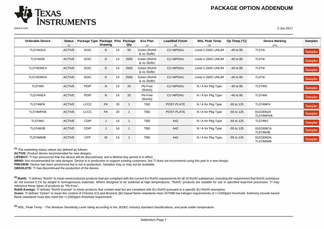
PACKAGE OPTION ADDENDUM
www.ti.com 2-Jun-2017
Addendum-Page 7
Orderable Device Status(1)
Package Type PackageDrawing
Pins PackageQty
Eco Plan(2)
Lead/Ball Finish(6)
MSL Peak Temp(3)
Op Temp (°C) Device Marking(4/5)
Samples
TL074IDG4 ACTIVE SOIC D 14 50 Green (RoHS& no Sb/Br)
CU NIPDAU Level-1-260C-UNLIM -40 to 85 TL074I
TL074IDR ACTIVE SOIC D 14 2500 Green (RoHS& no Sb/Br)
CU NIPDAU Level-1-260C-UNLIM -40 to 85 TL074I
TL074IDRE4 ACTIVE SOIC D 14 2500 Green (RoHS& no Sb/Br)
CU NIPDAU Level-1-260C-UNLIM -40 to 85 TL074I
TL074IDRG4 ACTIVE SOIC D 14 2500 Green (RoHS& no Sb/Br)
CU NIPDAU Level-1-260C-UNLIM -40 to 85 TL074I
TL074IN ACTIVE PDIP N 14 25 Pb-Free(RoHS)
CU NIPDAU N / A for Pkg Type -40 to 85 TL074IN
TL074INE4 ACTIVE PDIP N 14 25 Pb-Free(RoHS)
CU NIPDAU N / A for Pkg Type -40 to 85 TL074IN
TL074MFK ACTIVE LCCC FK 20 1 TBD POST-PLATE N / A for Pkg Type -55 to 125 TL074MFK
TL074MFKB ACTIVE LCCC FK 20 1 TBD POST-PLATE N / A for Pkg Type -55 to 125 81023062ATL074MFKB
TL074MJ ACTIVE CDIP J 14 1 TBD A42 N / A for Pkg Type -55 to 125 TL074MJ
TL074MJB ACTIVE CDIP J 14 1 TBD A42 N / A for Pkg Type -55 to 125 8102306CATL074MJB
TL074MWB ACTIVE CFP W 14 1 TBD A42 N / A for Pkg Type -55 to 125 8102306DATL074MWB
(1) The marketing status values are defined as follows:ACTIVE: Product device recommended for new designs.LIFEBUY: TI has announced that the device will be discontinued, and a lifetime-buy period is in effect.NRND: Not recommended for new designs. Device is in production to support existing customers, but TI does not recommend using this part in a new design.PREVIEW: Device has been announced but is not in production. Samples may or may not be available.OBSOLETE: TI has discontinued the production of the device.
(2) RoHS: TI defines "RoHS" to mean semiconductor products that are compliant with the current EU RoHS requirements for all 10 RoHS substances, including the requirement that RoHS substancedo not exceed 0.1% by weight in homogeneous materials. Where designed to be soldered at high temperatures, "RoHS" products are suitable for use in specified lead-free processes. TI mayreference these types of products as "Pb-Free".RoHS Exempt: TI defines "RoHS Exempt" to mean products that contain lead but are compliant with EU RoHS pursuant to a specific EU RoHS exemption.Green: TI defines "Green" to mean the content of Chlorine (Cl) and Bromine (Br) based flame retardants meet JS709B low halogen requirements of <=1000ppm threshold. Antimony trioxide basedflame retardants must also meet the <=1000ppm threshold requirement.
(3) MSL, Peak Temp. - The Moisture Sensitivity Level rating according to the JEDEC industry standard classifications, and peak solder temperature.

PACKAGE OPTION ADDENDUM
www.ti.com 2-Jun-2017
Addendum-Page 8
(4) There may be additional marking, which relates to the logo, the lot trace code information, or the environmental category on the device.
(5) Multiple Device Markings will be inside parentheses. Only one Device Marking contained in parentheses and separated by a "~" will appear on a device. If a line is indented then it is a continuationof the previous line and the two combined represent the entire Device Marking for that device.
(6) Lead/Ball Finish - Orderable Devices may have multiple material finish options. Finish options are separated by a vertical ruled line. Lead/Ball Finish values may wrap to two lines if the finishvalue exceeds the maximum column width.
Important Information and Disclaimer:The information provided on this page represents TI's knowledge and belief as of the date that it is provided. TI bases its knowledge and belief on informationprovided by third parties, and makes no representation or warranty as to the accuracy of such information. Efforts are underway to better integrate information from third parties. TI has taken andcontinues to take reasonable steps to provide representative and accurate information but may not have conducted destructive testing or chemical analysis on incoming materials and chemicals.TI and TI suppliers consider certain information to be proprietary, and thus CAS numbers and other limited information may not be available for release.
In no event shall TI's liability arising out of such information exceed the total purchase price of the TI part(s) at issue in this document sold by TI to Customer on an annual basis.
OTHER QUALIFIED VERSIONS OF TL072, TL072M, TL074, TL074M :
• Catalog: TL072, TL074
• Enhanced Product: TL072-EP, TL072-EP, TL074-EP, TL074-EP
• Military: TL072M, TL074M
NOTE: Qualified Version Definitions:
• Catalog - TI's standard catalog product
• Enhanced Product - Supports Defense, Aerospace and Medical Applications
• Military - QML certified for Military and Defense Applications

TAPE AND REEL INFORMATION
*All dimensions are nominal
Device PackageType
PackageDrawing
Pins SPQ ReelDiameter
(mm)
ReelWidth
W1 (mm)
A0(mm)
B0(mm)
K0(mm)
P1(mm)
W(mm)
Pin1Quadrant
TL071ACDR SOIC D 8 2500 330.0 12.4 6.4 5.2 2.1 8.0 12.0 Q1
TL071BCDR SOIC D 8 2500 330.0 12.4 6.4 5.2 2.1 8.0 12.0 Q1
TL071CDR SOIC D 8 2500 330.0 12.4 6.4 5.2 2.1 8.0 12.0 Q1
TL071CDR SOIC D 8 2500 330.0 12.4 6.4 5.2 2.1 8.0 12.0 Q1
TL071CPSR SO PS 8 2000 330.0 16.4 8.2 6.6 2.5 12.0 16.0 Q1
TL071IDR SOIC D 8 2500 330.0 12.4 6.4 5.2 2.1 8.0 12.0 Q1
TL072ACDR SOIC D 8 2500 330.0 12.4 6.4 5.2 2.1 8.0 12.0 Q1
TL072BCDR SOIC D 8 2500 330.0 12.4 6.4 5.2 2.1 8.0 12.0 Q1
TL072CDR SOIC D 8 2500 330.0 12.4 6.4 5.2 2.1 8.0 12.0 Q1
TL072CDR SOIC D 8 2500 330.0 12.4 6.4 5.2 2.1 8.0 12.0 Q1
TL072CPSR SO PS 8 2000 330.0 16.4 8.2 6.6 2.5 12.0 16.0 Q1
TL072CPWR TSSOP PW 8 2000 330.0 12.4 7.0 3.6 1.6 8.0 12.0 Q1
TL072IDR SOIC D 8 2500 330.0 12.4 6.4 5.2 2.1 8.0 12.0 Q1
TL072IDR SOIC D 8 2500 330.0 12.4 6.4 5.2 2.1 8.0 12.0 Q1
TL074ACDR SOIC D 14 2500 330.0 16.4 6.5 9.0 2.1 8.0 16.0 Q1
TL074ACNSR SO NS 14 2000 330.0 16.4 8.2 10.5 2.5 12.0 16.0 Q1
TL074BCDR SOIC D 14 2500 330.0 16.4 6.5 9.0 2.1 8.0 16.0 Q1
TL074CDR SOIC D 14 2500 330.0 16.4 6.5 9.0 2.1 8.0 16.0 Q1
PACKAGE MATERIALS INFORMATION
www.ti.com 18-Apr-2017
Pack Materials-Page 1

Device PackageType
PackageDrawing
Pins SPQ ReelDiameter
(mm)
ReelWidth
W1 (mm)
A0(mm)
B0(mm)
K0(mm)
P1(mm)
W(mm)
Pin1Quadrant
TL074CDRG4 SOIC D 14 2500 330.0 16.4 6.5 9.0 2.1 8.0 16.0 Q1
TL074CPWR TSSOP PW 14 2000 330.0 12.4 6.9 5.6 1.6 8.0 12.0 Q1
TL074IDR SOIC D 14 2500 330.0 16.4 6.5 9.0 2.1 8.0 16.0 Q1
*All dimensions are nominal
Device Package Type Package Drawing Pins SPQ Length (mm) Width (mm) Height (mm)
TL071ACDR SOIC D 8 2500 340.5 338.1 20.6
TL071BCDR SOIC D 8 2500 340.5 338.1 20.6
TL071CDR SOIC D 8 2500 367.0 367.0 35.0
TL071CDR SOIC D 8 2500 340.5 338.1 20.6
TL071CPSR SO PS 8 2000 367.0 367.0 38.0
TL071IDR SOIC D 8 2500 340.5 338.1 20.6
TL072ACDR SOIC D 8 2500 340.5 338.1 20.6
TL072BCDR SOIC D 8 2500 340.5 338.1 20.6
TL072CDR SOIC D 8 2500 340.5 338.1 20.6
TL072CDR SOIC D 8 2500 367.0 367.0 35.0
TL072CPSR SO PS 8 2000 367.0 367.0 38.0
TL072CPWR TSSOP PW 8 2000 367.0 367.0 35.0
TL072IDR SOIC D 8 2500 340.5 338.1 20.6
TL072IDR SOIC D 8 2500 367.0 367.0 35.0
PACKAGE MATERIALS INFORMATION
www.ti.com 18-Apr-2017
Pack Materials-Page 2

Device Package Type Package Drawing Pins SPQ Length (mm) Width (mm) Height (mm)
TL074ACDR SOIC D 14 2500 333.2 345.9 28.6
TL074ACNSR SO NS 14 2000 367.0 367.0 38.0
TL074BCDR SOIC D 14 2500 333.2 345.9 28.6
TL074CDR SOIC D 14 2500 333.2 345.9 28.6
TL074CDRG4 SOIC D 14 2500 333.2 345.9 28.6
TL074CPWR TSSOP PW 14 2000 367.0 367.0 35.0
TL074IDR SOIC D 14 2500 333.2 345.9 28.6
PACKAGE MATERIALS INFORMATION
www.ti.com 18-Apr-2017
Pack Materials-Page 3


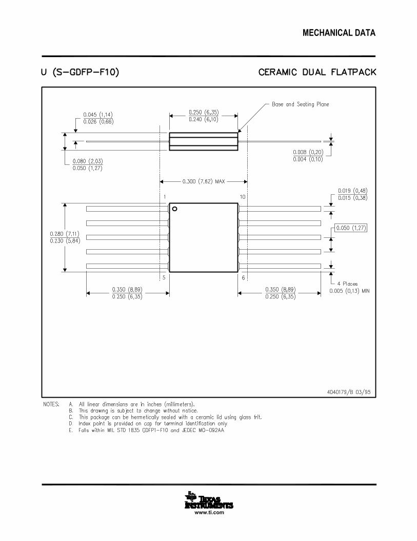


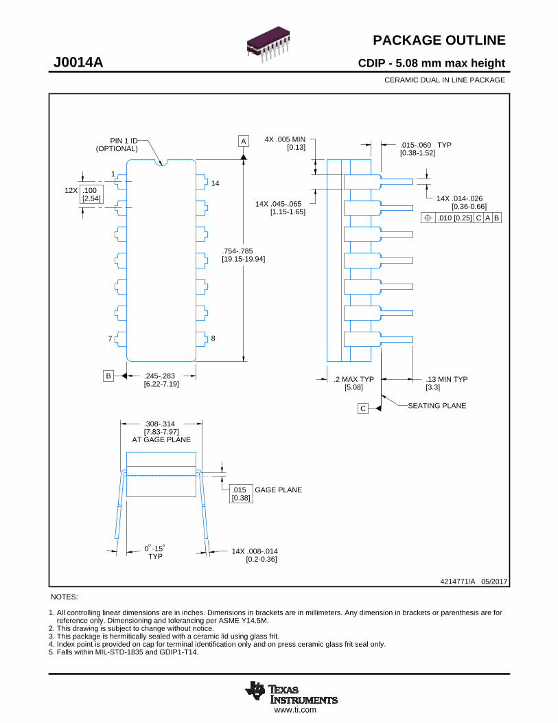
www.ti.com
PACKAGE OUTLINE
C
14X .008-.014 [0.2-0.36]TYP
-150
AT GAGE PLANE
-.314.308-7.977.83[ ]
14X -.026.014-0.660.36[ ]14X -.065.045
-1.651.15[ ]
.2 MAX TYP[5.08]
.13 MIN TYP[3.3]
TYP-.060.015-1.520.38[ ]
4X .005 MIN[0.13]
12X .100[2.54]
.015 GAGE PLANE[0.38]
A
-.785.754-19.9419.15[ ]
B -.283.245-7.196.22[ ]
CDIP - 5.08 mm max heightJ0014ACERAMIC DUAL IN LINE PACKAGE
4214771/A 05/2017
NOTES: 1. All controlling linear dimensions are in inches. Dimensions in brackets are in millimeters. Any dimension in brackets or parenthesis are for reference only. Dimensioning and tolerancing per ASME Y14.5M.2. This drawing is subject to change without notice. 3. This package is hermitically sealed with a ceramic lid using glass frit.4. Index point is provided on cap for terminal identification only and on press ceramic glass frit seal only.5. Falls within MIL-STD-1835 and GDIP1-T14.
7 8
141
PIN 1 ID(OPTIONAL)
SCALE 0.900
SEATING PLANE
.010 [0.25] C A B

www.ti.com
EXAMPLE BOARD LAYOUT
ALL AROUND[0.05]
MAX.002
.002 MAX[0.05]ALL AROUND
SOLDER MASKOPENING
METAL
(.063)[1.6]
(R.002 ) TYP[0.05]
14X ( .039)[1]
( .063)[1.6]
12X (.100 )[2.54]
(.300 ) TYP[7.62]
CDIP - 5.08 mm max heightJ0014ACERAMIC DUAL IN LINE PACKAGE
4214771/A 05/2017
LAND PATTERN EXAMPLENON-SOLDER MASK DEFINED
SCALE: 5X
SEE DETAIL A SEE DETAIL B
SYMM
SYMM
1
7 8
14
DETAIL ASCALE: 15X
SOLDER MASKOPENING
METAL
DETAIL B13X, SCALE: 15X
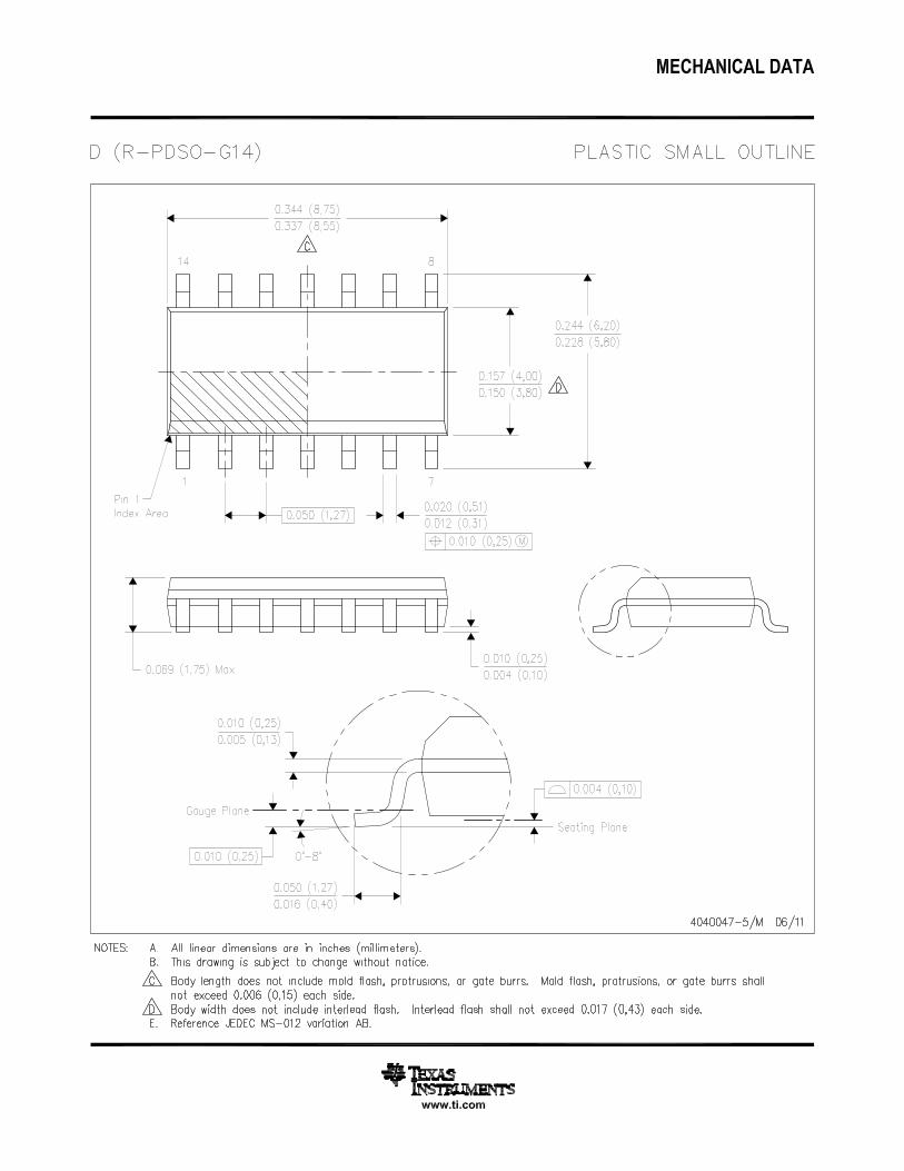
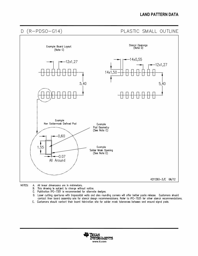
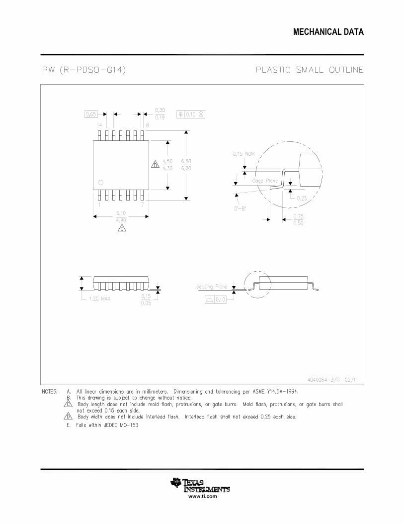

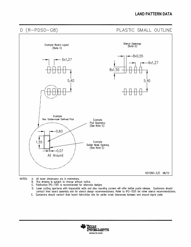


MECHANICAL DATA
MCER001A – JANUARY 1995 – REVISED JANUARY 1997
POST OFFICE BOX 655303 • DALLAS, TEXAS 75265
JG (R-GDIP-T8) CERAMIC DUAL-IN-LINE
0.310 (7,87)0.290 (7,37)
0.014 (0,36)0.008 (0,20)
Seating Plane
4040107/C 08/96
5
40.065 (1,65)0.045 (1,14)
8
1
0.020 (0,51) MIN
0.400 (10,16)0.355 (9,00)
0.015 (0,38)0.023 (0,58)
0.063 (1,60)0.015 (0,38)
0.200 (5,08) MAX
0.130 (3,30) MIN
0.245 (6,22)0.280 (7,11)
0.100 (2,54)
0°–15°
NOTES: A. All linear dimensions are in inches (millimeters).B. This drawing is subject to change without notice.C. This package can be hermetically sealed with a ceramic lid using glass frit.D. Index point is provided on cap for terminal identification.E. Falls within MIL STD 1835 GDIP1-T8


www.ti.com
PACKAGE OUTLINE
C
TYP6.66.2
1.2 MAX
6X 0.65
8X 0.300.19
2X1.95
0.150.05
(0.15) TYP
0 - 8
0.25GAGE PLANE
0.750.50
A
NOTE 3
3.12.9
BNOTE 4
4.54.3
4221848/A 02/2015
TSSOP - 1.2 mm max heightPW0008ASMALL OUTLINE PACKAGE
NOTES: 1. All linear dimensions are in millimeters. Any dimensions in parenthesis are for reference only. Dimensioning and tolerancing per ASME Y14.5M. 2. This drawing is subject to change without notice. 3. This dimension does not include mold flash, protrusions, or gate burrs. Mold flash, protrusions, or gate burrs shall not exceed 0.15 mm per side. 4. This dimension does not include interlead flash. Interlead flash shall not exceed 0.25 mm per side.5. Reference JEDEC registration MO-153, variation AA.
18
0.1 C A B
54
PIN 1 IDAREA
SEATING PLANE
0.1 C
SEE DETAIL A
DETAIL ATYPICAL
SCALE 2.800

www.ti.com
EXAMPLE BOARD LAYOUT
(5.8)
0.05 MAXALL AROUND
0.05 MINALL AROUND
8X (1.5)8X (0.45)
6X (0.65)
(R )TYP
0.05
4221848/A 02/2015
TSSOP - 1.2 mm max heightPW0008ASMALL OUTLINE PACKAGE
SYMM
SYMM
LAND PATTERN EXAMPLESCALE:10X
1
45
8
NOTES: (continued) 6. Publication IPC-7351 may have alternate designs. 7. Solder mask tolerances between and around signal pads can vary based on board fabrication site.
METALSOLDER MASKOPENING
NON SOLDER MASKDEFINED
SOLDER MASK DETAILSNOT TO SCALE
SOLDER MASKOPENING
METAL UNDERSOLDER MASK
SOLDER MASKDEFINED
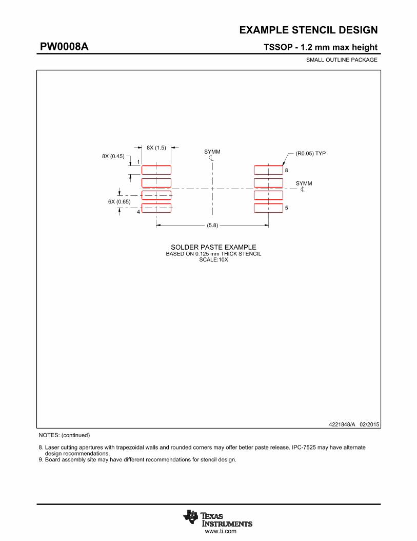
www.ti.com
EXAMPLE STENCIL DESIGN
(5.8)
6X (0.65)
8X (0.45)8X (1.5)
(R ) TYP0.05
4221848/A 02/2015
TSSOP - 1.2 mm max heightPW0008ASMALL OUTLINE PACKAGE
NOTES: (continued) 8. Laser cutting apertures with trapezoidal walls and rounded corners may offer better paste release. IPC-7525 may have alternate design recommendations. 9. Board assembly site may have different recommendations for stencil design.
SYMM
SYMM
1
45
8
SOLDER PASTE EXAMPLEBASED ON 0.125 mm THICK STENCIL
SCALE:10X

IMPORTANT NOTICE
Texas Instruments Incorporated (TI) reserves the right to make corrections, enhancements, improvements and other changes to itssemiconductor products and services per JESD46, latest issue, and to discontinue any product or service per JESD48, latest issue. Buyersshould obtain the latest relevant information before placing orders and should verify that such information is current and complete.TI’s published terms of sale for semiconductor products (http://www.ti.com/sc/docs/stdterms.htm) apply to the sale of packaged integratedcircuit products that TI has qualified and released to market. Additional terms may apply to the use or sale of other types of TI products andservices.Reproduction of significant portions of TI information in TI data sheets is permissible only if reproduction is without alteration and isaccompanied by all associated warranties, conditions, limitations, and notices. TI is not responsible or liable for such reproduceddocumentation. Information of third parties may be subject to additional restrictions. Resale of TI products or services with statementsdifferent from or beyond the parameters stated by TI for that product or service voids all express and any implied warranties for theassociated TI product or service and is an unfair and deceptive business practice. TI is not responsible or liable for any such statements.Buyers and others who are developing systems that incorporate TI products (collectively, “Designers”) understand and agree that Designersremain responsible for using their independent analysis, evaluation and judgment in designing their applications and that Designers havefull and exclusive responsibility to assure the safety of Designers' applications and compliance of their applications (and of all TI productsused in or for Designers’ applications) with all applicable regulations, laws and other applicable requirements. Designer represents that, withrespect to their applications, Designer has all the necessary expertise to create and implement safeguards that (1) anticipate dangerousconsequences of failures, (2) monitor failures and their consequences, and (3) lessen the likelihood of failures that might cause harm andtake appropriate actions. Designer agrees that prior to using or distributing any applications that include TI products, Designer willthoroughly test such applications and the functionality of such TI products as used in such applications.TI’s provision of technical, application or other design advice, quality characterization, reliability data or other services or information,including, but not limited to, reference designs and materials relating to evaluation modules, (collectively, “TI Resources”) are intended toassist designers who are developing applications that incorporate TI products; by downloading, accessing or using TI Resources in anyway, Designer (individually or, if Designer is acting on behalf of a company, Designer’s company) agrees to use any particular TI Resourcesolely for this purpose and subject to the terms of this Notice.TI’s provision of TI Resources does not expand or otherwise alter TI’s applicable published warranties or warranty disclaimers for TIproducts, and no additional obligations or liabilities arise from TI providing such TI Resources. TI reserves the right to make corrections,enhancements, improvements and other changes to its TI Resources. TI has not conducted any testing other than that specificallydescribed in the published documentation for a particular TI Resource.Designer is authorized to use, copy and modify any individual TI Resource only in connection with the development of applications thatinclude the TI product(s) identified in such TI Resource. NO OTHER LICENSE, EXPRESS OR IMPLIED, BY ESTOPPEL OR OTHERWISETO ANY OTHER TI INTELLECTUAL PROPERTY RIGHT, AND NO LICENSE TO ANY TECHNOLOGY OR INTELLECTUAL PROPERTYRIGHT OF TI OR ANY THIRD PARTY IS GRANTED HEREIN, including but not limited to any patent right, copyright, mask work right, orother intellectual property right relating to any combination, machine, or process in which TI products or services are used. Informationregarding or referencing third-party products or services does not constitute a license to use such products or services, or a warranty orendorsement thereof. Use of TI Resources may require a license from a third party under the patents or other intellectual property of thethird party, or a license from TI under the patents or other intellectual property of TI.TI RESOURCES ARE PROVIDED “AS IS” AND WITH ALL FAULTS. TI DISCLAIMS ALL OTHER WARRANTIES ORREPRESENTATIONS, EXPRESS OR IMPLIED, REGARDING RESOURCES OR USE THEREOF, INCLUDING BUT NOT LIMITED TOACCURACY OR COMPLETENESS, TITLE, ANY EPIDEMIC FAILURE WARRANTY AND ANY IMPLIED WARRANTIES OFMERCHANTABILITY, FITNESS FOR A PARTICULAR PURPOSE, AND NON-INFRINGEMENT OF ANY THIRD PARTY INTELLECTUALPROPERTY RIGHTS. TI SHALL NOT BE LIABLE FOR AND SHALL NOT DEFEND OR INDEMNIFY DESIGNER AGAINST ANY CLAIM,INCLUDING BUT NOT LIMITED TO ANY INFRINGEMENT CLAIM THAT RELATES TO OR IS BASED ON ANY COMBINATION OFPRODUCTS EVEN IF DESCRIBED IN TI RESOURCES OR OTHERWISE. IN NO EVENT SHALL TI BE LIABLE FOR ANY ACTUAL,DIRECT, SPECIAL, COLLATERAL, INDIRECT, PUNITIVE, INCIDENTAL, CONSEQUENTIAL OR EXEMPLARY DAMAGES INCONNECTION WITH OR ARISING OUT OF TI RESOURCES OR USE THEREOF, AND REGARDLESS OF WHETHER TI HAS BEENADVISED OF THE POSSIBILITY OF SUCH DAMAGES.Unless TI has explicitly designated an individual product as meeting the requirements of a particular industry standard (e.g., ISO/TS 16949and ISO 26262), TI is not responsible for any failure to meet such industry standard requirements.Where TI specifically promotes products as facilitating functional safety or as compliant with industry functional safety standards, suchproducts are intended to help enable customers to design and create their own applications that meet applicable functional safety standardsand requirements. Using products in an application does not by itself establish any safety features in the application. Designers mustensure compliance with safety-related requirements and standards applicable to their applications. Designer may not use any TI products inlife-critical medical equipment unless authorized officers of the parties have executed a special contract specifically governing such use.Life-critical medical equipment is medical equipment where failure of such equipment would cause serious bodily injury or death (e.g., lifesupport, pacemakers, defibrillators, heart pumps, neurostimulators, and implantables). Such equipment includes, without limitation, allmedical devices identified by the U.S. Food and Drug Administration as Class III devices and equivalent classifications outside the U.S.TI may expressly designate certain products as completing a particular qualification (e.g., Q100, Military Grade, or Enhanced Product).Designers agree that it has the necessary expertise to select the product with the appropriate qualification designation for their applicationsand that proper product selection is at Designers’ own risk. Designers are solely responsible for compliance with all legal and regulatoryrequirements in connection with such selection.Designer will fully indemnify TI and its representatives against any damages, costs, losses, and/or liabilities arising out of Designer’s non-compliance with the terms and provisions of this Notice.
Mailing Address: Texas Instruments, Post Office Box 655303, Dallas, Texas 75265Copyright © 2017, Texas Instruments Incorporated