TI’s Next Great Leap: Introducing the NexFET™ 100V Power MOSFETs!
40
TI’s Next Great Leap: Introducing the NexFET™ 100V Power MOSFETs!
-
Upload
design-world -
Category
Engineering
-
view
777 -
download
5
Transcript of TI’s Next Great Leap: Introducing the NexFET™ 100V Power MOSFETs!

TI’s Next Great Leap:
Introducing the NexFET™
100V Power MOSFETs!

This webinar will be available afterwards at
www.designworldonline.com & email
Q&A at the end of the presentation
Hashtag for this webinar: #DWwebinar
Before We Start

Moderator Presenter
Miles BudimirDesign World
Rich NowakowskiTexas Instruments

TI’s Next Great Leap: Introducing the
NexFET™ 100V Power MOSFETs!
April 2014
Rich NowakowskiTexas Instruments

Agenda• NexFET Technology and Advantages
• Mid Voltage NexFETs for Power Supplies
• Synchronous-Buck Design Example
• Flyback Design Example
• Forward Converter with Active Clamp Design Example
• NexFET for Motor Control
• Stepper Motors
• Brush & Brushless DC Motors
• Tools and Resources

TI expands NexFET™ portfolio with mid-voltage MOSFETs
• Excellent thermal performance
• Supports high-current motor control
and power conversion applications
• Lowest on-resistance 80V & 100V
MOSFETs in TO-220
CSD19506 at 2.0 milliohm Rds(on) at 80V
CSD19536 at 2.3 milliohm Rds(on) at 100V
WEBENCH® design tool support
Evaluation modules: DC brushless motor
control, digital power, POL
New MOSFETs in TO-220 & SON packages support 40V, 60V, 80V and 100V!

MV NexFET Gate Switching Speed
TI Best Cdv/dt Immunity & ~ Twice Switching Speed
-2.0
-1.0
0.0
1.0
2.0
3.0
4.0
5.0
6.0
0 250 500 750 1,000 1,250 1,500 1,750 2,000 2,250 2,500
Gate
Vol
tage
(V)
Time (ns)
Gate Switching Waveform
CSD18531Q5A
BSC031N06Competition

MV NEXFETTM Robustness / Avalanche Capability
0
20
40
60
80
100
120
140
UIS C
urre
nt (A
), 0.
1mH
Devices Tested
Avalanche Capability
CSD18501Q5A 25ºC
CSD18502Q5B 25ºC
BSC016N04 25ºC
125ºC25ºC
Leadership Ruggedness and Avalanche Capability
20% Higher Capability vs Leading Competitor
Devices tested
to failure
Competition

NexFET SON 5x6mm Devices
NexFET Dual SO-8 Devices
Part Number PackageBVDSS
(V)
VGS
(V)
RDS(ON)
Typ (10V)
(mΩ)
RDS(ON)
Max (10V)
(mΩ)
ID @
25ºC (silicon)
Qg(10)
Typ
(nC)
Qgd
Typ
(nC)
Qgs
Typ
(nC)
Qrr -
300A/µs
Typ
(nC)
Coss
Typ
(pF)
Alpha
SamplesRTM
CSD18509Q5B SON5x6 40 20 1.0 1.25 264 160 21.0 34.0 40 1100 30-Jan 14Q2
CSD18502Q5B SON5x6 40 20 1.8 2.3 204 52 8.4 10.3 88 900 Now Now
CSD18501Q5A SON5x6 40 20 2.5 3.2 155 42 5.9 8.1 70 725 Now Now
CSD18503Q5A SON5x6 40 20 3.4 4.3 145 27 4.3 4.5 52 510 Now Now
CSD18504Q5A SON5x6 40 20 5.3 6.6 75 16 2.4 3.2 39 310 Now Now
CSD18540Q5B SON5x6 60 20 1.6 2.0 188 58 11.0 12.8 120 498 15-Feb 14Q2
CSD18532Q5B SON5x6 60 20 2.5 3.2 169 44 6.9 10.0 111 470 Now Now
CSD18532NQ5B SON5x6 60 20 2.7 3.4 165 49 7.9 16.0 139 495 Now Now
CSD18531Q5A SON5x6 60 20 3.5 4.6 134 36 5.9 6.9 100 380 Now Now
CSD18533Q5A SON5x6 60 20 4.7 5.9 103 29 5.4 6.6 68 292 Now Now
CSD18563Q5A SON5x6 60 20 6.0 7.5 98 29 5.4 6.6 57 292 Now Now
CSD18534Q5A SON5x6 60 20 7.8 9.8 69 17 3.5 3.2 54 167 Now Now
CSD18537NQ5A SON5x6 60 20 11 14 55 14 2.3 4.7 54 136 Now Now
CSD19502Q5B SON5x6 80 20 3.4 4.1 138 48 8.6 14 275 925 Now Now
CSD19532Q5B SON5x6 100 20 4.0 4.9 130 48 8.7 13 249 706 Now Now
CSD19531Q5A SON5x6 100 20 5.3 6.4 110 37 7.0 11 226 540 Now Now
CSD19533Q5A SON5x6 100 20 7.8 9.4 75 27 4.9 7.9 163 395 Now Now
CSD19534Q5A SON5x6 100 20 12.4 15.5 53 15 2.7 4.5 97 228 Now 10-Feb
Part Number PackageBVDSS
(V)
VGS
(V)
RDS(ON)
Typ (10V)
(mΩ)
RDS(ON)
Max (10V)
(mΩ)
ID @
25ºC (silicon)
Qg(10)
Typ
(nC)
Qgd
Typ
(nC)
Qgs
Typ
(nC)
Qrr -
300A/µs
Typ
(nC)
Coss
Typ
(pF)
Alpha
SamplesRTM
CSD88537ND Dual SO-8 60 20 13 16 13 14 2.3 4.7 40 136 Now 5-Feb
CSD88539ND Dual SO-8 60 20 22 28 9.7 9 2.1 3.2 20 77 Now 5-Feb

TO-220 Devices
10
Part Number PackageBVDSS
(V)
VGS
(V)
RDS(ON)
Typ (10V)
(mΩ)
RDS(ON)
Max (10V)
(mΩ)
ID @
25ºC (silicon)
Qg(10)
Typ
(nC)
Qgd
Typ
(nC)
Qgs
Typ
(nC)
Qrr -
300A/µs
Typ
(nC)
Coss
Typ
(pF)
Alpha
SamplesRTM
CSD18502KCS TO-220 40 20 2.4 2.9 200 52 8.4 10.3 105 900 Now Now
CSD18503KCS TO-220 40 20 3.6 4.5 130 30 4.6 7.7 60 480 Now Now
CSD18504KCS TO-220 40 20 5.5 7.0 85 19 3.5 4.4 46 320 Now Now
CSD18532KCS TO-220 60 20 3.3 4.2 169 44 6.9 10.0 127 470 Now Now
CSD18533KCS TO-220 60 20 5.0 6.3 114 28 3.9 9.4 97 300 Now Now
CSD18534KCS TO-220 60 20 7.6 9.5 71 19 3.1 4.8 68 164 Now Now
CSD18537NKCS TO-220 60 20 11 14 54 14 2.3 5.2 77 136 Now Now
CSD19506KCS TO-220 80 20 2.0 2.5 250 125 23 37 800 1700 Now Now
CSD19505KCS TO-220 80 20 2.7 3.3 193 77 14 23 495 1050 Now 23-Jan
CSD19501KCS TO-220 80 20 5.6 7.0 113 36 6.6 11 233 497 Now 30-Jan
CSD19503KCS TO-220 80 20 7.6 9.2 94 28 5.4 9.8 161 555 Now Now
CSD19536KCS TO-220 100 20 2.2 2.8 238 125 23 37 800 1890 Now 27-Jan
CSD19535KCS TO-220 100 20 3.1 3.9 180 77 14 23 495 1170 Now 30-Jan
CSD19531KCS TO-220 100 20 6.3 7.9 102 37 7.0 12 270 560 Now Now
CSD19533KCS TO-220 100 20 8.7 10.5 86 27 5.4 9.0 151 395 Now Now

AC-DC
RectificationPFC
Load Sw
ORingDCAC
HV MOSFETS
500-800V
MV MOSFETS
40-100V
LV MOSFETS
25-30VSMPS TOPOLOGIES
• Non- Isolated Synchronous Buck
• Off-line Flyback <100W
• Forward with Active Clamp <250W
• Two-Transistor Forward TTF <500W
• Half Bridge with Synchronous Rectification <500W
• Resonant LLC/ Series Resonant SRC <500W
• Full-Bridge Phase-Shifted ZVS <1000W
Power Supply Architecture

MV NexFETs for Synchronous Rectification
FOM for Synchronous Rectification
• FOM = RDS(on) * (Qrr+1/2 Qoss)
- Qrr measured at transformer secondary side di/dt
- Qoss measured at transformer voltage on secondary side
MV MOSFETS Selection Criteria
• FET BV depends on Vout and Transformer Turns Ratio N ( N=Np/Ns)
• FET RDS(on) selection depends on SMPS topology, Iout and Pout

Non-Isolated Synchronous-Buck Example• VIN – 24V, 36V
• VOUT – 5V
• IOUT – 5A
• LOUT – 10µH (14mΩ DCR)
• Frequency – 100kHz
• Controller – TPS40170
• EVM Used
o TPS40170-578 EVM
• High Side FET
o CSD18537NQ5A
• Low Side FET
o CSD18563Q5A
• Ringing Reduction
o RBoot_Strap = 5.6Ωo CSnubber = 820pF
o RSnubber = 3 Ω
13
CSD18537NQ5A
CSD18537NQ5A

10A CSD18537NQ5A/CSD18563Q5A 60V, Industrial NexFET™ for Synchronous Buck Controllers
• Up to 10A low side buck converters
• >92% Peak Efficiency with 36VIN/5VOUT
• >93% Peak Efficiency with 24VIN/5VOUT
• Space saving SON5x6mm
package
• Low thermal resistance
• Ultra Low Qg and Qgd
• Low-side improved softness factor
• Small size and good thermal
performance
• Excellent light-load efficiency
• Minimized switch node ringing
• 63% de-rating with 36VIN

10A / 36Vin Switch-Node Waveforms36VIN , 5VOUT, 100kHz, 10A,
No Ringing Reductions
Peak Ring – 46.4V Peak Ring – 38.2V
36VIN , 5VOUT, 100kHz, 10A, w/
Ringing Reductions
Implementing Snubber and Bootstrap Resistor achieves 63% De-Rating

TI’s Most Popular Wide-Vin Buck Controllers
Visit www.ti.com/widevin for more information...

Recommended NexFETs for Buck Controllers
DC Solution HS FET LS FET Comments
60V Low-Current CSD19534Q5A CSD19534Q5A VIN 10 to 60V
IOUT up to 5A
Up to 600kHz
60V High-Current CSD19534Q5A CSD19533Q5A VIN 10 to 60V
IOUT up to 10A
Up to 600kHz
40V Low-Current CSD18537NQ5A CSD18537NQ5A VIN 10 to 40V
IOUT up to 5A
Up to 600kHz
40V High-Current CSD18537NQ5A CSD18563Q5A VIN 10 to 40V
IOUT up to 10A
Up to 600kHz
For higher currents, parallel the high-current high-side and low-side MOSFETs

Q2 Q1 Sync Rectifier
Q2 Primary Side FET
CrCM/ QR Flyback for AC-DC Applications
Choosing the FET Q1
• Low Rds(on) from 2-10mΩ
• Low Rds(on) affects Diode Emulation
• Use 60V FET for 5Vout
• Use 100V FET for 19.5Vout
• <40W, QFN package
• <125W, 1 to 2 FETs in a TO-220
Operating on Critical Conduction Mode
.

MOSFET VDS On-Resistance
Primary
FET Q2
650V – 800V ≤ 1Ω for 20W
≤ 300mΩ for 95W
Synchronous Rectifier FET Q160V for 5Vout
100V for ≤ 20Vout
2 - 10mΩ
60V CSD18531Q5A
60V CSD18533Q5A
100V CSD19531Q5A
100V CSD19531KCS
100V CSD19532Q5B
100V CSD19535KCS
AC Adaptors: Universal Input 85 - 265Vac , F = 50/60Hz
Fsw = 50 - 150kHz
Vout = 1.5V - 19.5V, Pout ≤ 150w
Suggested Mid-Voltage NEXFETs - Flyback
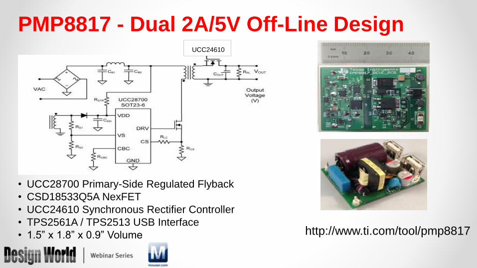
PMP8817 - Dual 2A/5V Off-Line Design
• UCC28700 Primary-Side Regulated Flyback
• CSD18533Q5A NexFET
• UCC24610 Synchronous Rectifier Controller
• TPS2561A / TPS2513 USB Interface
• 1.5” x 1.8” x 0.9” Volume
UCC24610
http://www.ti.com/tool/pmp8817

PMP8817 Efficiency Plot

Forward Converter with Active Clamp Example
Q3
Q4
Q1 Forward FET
Q2 Freewheeling FET
Q3 Active Clamp FET
Q4 Primary FET
Choosing the FETs Q1 & Q2
• Forward FET Q1 optimized for fast switching, low Qg &
low turn-off loss
• Freewheeling FET Q2 optimized for low conduction loss
and best SRs FOM (RDS(on) * Qrr)
• The number of paralleled FETs depends on the power
level and the efficiency target.
Features
• Gate drivers not needed
for Q1 & Q2. Easy to
control
• Higher efficiency operation
as reset energy is
conserved, not dissipated!
• Zero-Voltage Switching
achievable
• Transformer smaller than
regular Forward as it
utilizes more of the flux of
transformer core

Suggested NexFETs -Forward Converter with Active Clamp
SolutionPrimary
FET Q4
Active
Clamp
FET Q3
Forward
FET Q2
Freewheeling
FET Q3
DC-DC
36 – 75Vin
150V 150V
60V CSD18531Q5A
100V CSD19531Q5A
100V CSD19533Q5A
40V CSD18502Q5B
40V CSD18509Q5B
60V CSD18532Q5B
60V CSD18540Q5B
AC-DC Offline
85 – 265Vac
800V 650V
80V CSD19501KCS
100V CSD19531Q5A
100V CSD19531KCS
60V CSD18532Q5B
60V CSD18540Q5B
60V CSD18532KCS
Off-line AC-DC Isolated
• VIN = 85 – 265VAC, VOUT = 5 – 12V, POUT ≤250W
DC - DC Isolated Converter - Telecom, POE and Computing
• VIN = 36 – 75V, VOUT ≤ 12V, IOUT = 0 – 25A, FSW = 250kHz

PMP7499 12V/5A Active Clamp Forward
TI Devices
• UCC2897A Active Clamp PWM Controller
• CSD18533Q5A NexFET
• TPS2379 PD Controller http://www.ti.com/tool/pmp7499

PMP7499 Efficiency Plot

Resonant LLC DC-DC Converter
Resonant LLC
• Variable frequency converter
• Eliminates switching losses in
primary FETs
• No output inductor
Choosing the FETs S1 & S2
• Controls voltage stress on output
synchronous rectifiers. Use lower rated FETs
S1 & S2
• Turned on at Zero Current Switching –
reduces gate drive losses
• Driven by secondary-side controller

Resonant LLC DC/DC Converter
MOSFET MOSFET BV RDS(ON) Recommended FET
Primary FET Q1/Q2 500-650V 100-300 mΩ N/A
Sync Rectifier FET
S1/S2
40V for VOUT = 12V
60V for VOUT = 15V1 – 3mΩ
40V CSD18502Q5B
40V CSD18509Q5B
60V CSD18532Q5B
60V CSD18540Q5B
Vin = 350-400VDC, Vout = 12V, Iout = 0-50A, Fsw = 100 – 500kHz

PMP5967: 400VDC 12V @ 460W Design
TI Devices
• UCC25600 Resonant LLC PWM Controller
• CSD18501Q5A NexFET
• UCC24610 Secondary Side Controller www.ti.com/tool/pmp5967

PMP5967 Efficiency Plot

Motor Control
Solutions

• Current ratings and SOA are the selection criteria, not MOSFET On-
resistance
• Ruggedness and UIS (Unclamped Inductive Switching) avalanche
capability are important
• Survive rotor-stalled condition for extended intervals of time
MOSFET Selection for Motor Control

CSD88537ND & CSD88539ND60-20V, Dual N-channel NexFET™ Power MOSFETs
• Brushless DC Motor Control
3 Phase Topology
Up to 9A stall current
• Stepper Motor Control
Full Bridge Topology
(2 Phase)
• Space Saving Dual SO-8
Package
• 3V Standard Threshold
• Low Thermal Resistance
• Ultra Low Qg and Qgd
• 50% Footprint Reduction over Discrete
SON5x6 or SO-8
~4A per FET for CSD88539ND
~8A per FET for CSD88537ND
• Cost competitive solution

NexFETs for Stepper Motor Control
• TI Motor Controller DRV8711EVM Uses
CSD18531Q5A
• Textile Machines
• ATM Machines
• Vending Machines
• Industrial Automation
CSD18537NQ5A 60V BVDSS
SON5x6
11 mΩ Rds(on)
50A Capability
CSD88537ND 60V BVDSS
Dual in SO-8
~12.5 mΩ Rds(on)
8A Capability
CSD88539ND 60V BVDSS
Dual in SO-8
23 mΩ Rds(on)
4A Capability

NexFETs for DC Stepper Motor Operation
Recommendation for Dual Full-Bridge DC Stepper MotorPre-Driver Imotor NexFET ™ # FETs BVDSS Package
DRV8711 ≤3A CSD88539ND 4x 60V Dual SO-8
DRV8711 ≤6A CSD88537ND 4x 60V Dual SO-8
DRV8711 ≤15A CSD18531Q5A 8x 60V SON5x6

Power Tool Internal Circuit
NexFETs for Brush DC Motor Drive: Choppers
• Li-Ion batteries: 3.6V / 7.2V ... 22V
• Trigger speed ≥ 70%, FSW= 4 – 10kHz
MOSFET performance required in Power Tools:
Survive extended Stalled-Rotor condition
• Ton = 1s/ Toff = 10S Ipeak = 165A
VBATT MOSFET BV Silicon IDM Recommended FET
≤12V 30V 80-150A 30V CSD17556Q5B
18V 40-60V 100-180A40V CSD18502KCS
60V CSD18532KCS
24V 60-80V 100-240A60V CSD18532KCS
80V CSD19506KCS
42 – 48V 100V ≤100A 100V CSD19536KCS

NexFETs for 3-Phase BLDC Motor Control
• DRV8301
• DRV8302
• DRV3201-Q1
• DRV3202-Q1
• DRV3211-Q1
CSD18502Q5B 40V BVDSS
SON5x6 Package
1.8 mΩ RDS(on)
100A Capability
CSD18502KCS 40V BVDSS
TO-220 Package
2.4 mΩ RDS(on)
100A Capability
CSD18508Q5B 40V BVDSS
SON5x6 Package
1.3 mΩ RDS(on)
100A Capability

Key Mid Voltage Evaluation Modules
• Stepper motor pre-driver: DRV8711EVM evaluation module is based on the DRV8711 stepper motor controller paired with a NexFET device to drive a bipolar stepper motor or two brushed DC motors.
• Motor Drive BoosterPack: The BOOSTXL-DRV8301 kit is a 10-A, 3-phase brushless DC drive stage based on the DRV8301 pre-driver -- designed for those learning about sensor-less brushless control techniques and drive stage design.
• Digital power: UCD3138PSFBEVM-027 allows power developers to design a digitally controlled, phase-shifted off-line, 12-V, 360-W power converter application.
• Point-of-load control: TPS40170EVM-597 evaluation board features TI’s TPS40170 synchronous step-down controllers with two NexFET devices.

Thank You!
• TI Now Offers up to 100V NexFET™ Power MOSFETs for Switching Applications and Motor Control
• Opening up new range of 40-100V FETs thru 1Q and 2Q2014
• Visit our NexFET™ landing page: www.ti/com/nexfet

Questions?
Miles BudimirDesign [email protected]
Phone: 440.234.4531
Twitter: @DW_Motion
Rich NowakowskiTexas [email protected]
Phone: 214-480-1667

Thank You
This webinar will be available at
designworldonline.com & email
Tweet with hashtag #DWwebinar
Connect with Design World
Discuss this on EngineeringExchange.com