TIMERS IN PIC MICROCONTROLLER OBJECTIVE...
13
EEE394 Microprocessor and Microcontroller Laboratory Lab #5 Department of Electrical & Electronics Engineering, Amrita Vishwa Vidyapeetham, Coimbatore Page 44 Exp. No #5 Date: TIMERS IN PIC MICROCONTROLLER OBJECTIVE The purpose of the experiment is to configure the timer0 & timer1 peripheral registers for applications. (i) To turn-on the LED connected to port with software delay (ii) To turn-on the LED connected to port with Timer0 module. (iii) To turn-on the LED connected to port with Timer1 module. PRE-LAB Complete the following study before starting the lab • PIC16F877A Timer0 & Timer1 Module • MPLAB IDE • PROTEUS THEORY PIC16F877A consist of three Timer Modules i.e Timer-0, Timer-1 and Timer-2. Every Timer needs a clock pulse to tick. The Clock Source can be internal or external. If the internal clock source is used, then 1/4th of the frequency of the Crystal Oscillator on the OSC1 and OSC2 pins (FOSC/4) is fed into the Timer. TIMER0 Module The main timing/counting features of Timer-0 module are given below. Timer-0 module has built in 8 bit timer/counter It can be easily readable/writable Built in 8 bit software programmable pre-scalar functions Easily select internal/external clock pulses Interrupt with overflow from the value FFh to 00h Edge selection for external clock pulse The timer mode is normally selected by clearing the T0CS bit in the register. Counter mode is selected by setting bit T0CS in Counter mode. Timer 0 will increment either on every rising or falling edge of pin RA4/T0CKI. The incrementing edge is determined by the Timer 0 Source Edge Select bit, T0SE. Clearing bit T0SE selects the rising edge. The pre-scaler is mutually exclusively shared between the Timer0 module and the Watchdog Timer.
Transcript of TIMERS IN PIC MICROCONTROLLER OBJECTIVE...
EEE394 Microprocessor and Microcontroller Laboratory Lab #5
Department of Electrical & Electronics Engineering, Amrita Vishwa Vidyapeetham, Coimbatore
Page 44
Exp. No #5 Date:
TIMERS IN PIC MICROCONTROLLER
OBJECTIVE
The purpose of the experiment is to configure the timer0 & timer1 peripheral registers for applications. (i) To turn-on the LED connected to port with software delay (ii) To turn-on the LED connected to port with Timer0 module. (iii) To turn-on the LED connected to port with Timer1 module.
PRE-LAB
Complete the following study before starting the lab
• PIC16F877A Timer0 & Timer1 Module
• MPLAB IDE
• PROTEUS
THEORY
PIC16F877A consist of three Timer Modules i.e Timer-0, Timer-1 and Timer-2. Every Timer needs a clock pulse to
tick. The Clock Source can be internal or external. If the internal clock source is used, then 1/4th of the frequency
of the Crystal Oscillator on the OSC1 and OSC2 pins (FOSC/4) is fed into the Timer.
TIMER0 Module
The main timing/counting features of Timer-0 module are given below.
Timer-0 module has built in 8 bit timer/counter
It can be easily readable/writable
Built in 8 bit software programmable pre-scalar functions
Easily select internal/external clock pulses
Interrupt with overflow from the value FFh to 00h
Edge selection for external clock pulse
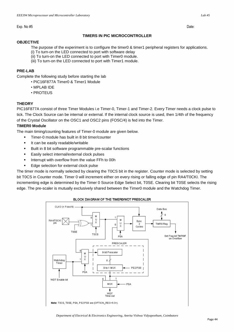
The timer mode is normally selected by clearing the T0CS bit in the register. Counter mode is selected by setting
bit T0CS in Counter mode. Timer 0 will increment either on every rising or falling edge of pin RA4/T0CKI. The
incrementing edge is determined by the Timer 0 Source Edge Select bit, T0SE. Clearing bit T0SE selects the rising
edge. The pre-scaler is mutually exclusively shared between the Timer0 module and the Watchdog Timer.
EEE394 Microprocessor and Microcontroller Laboratory Lab #5
Department of Electrical & Electronics Engineering, Amrita Vishwa Vidyapeetham, Coimbatore
Page 45
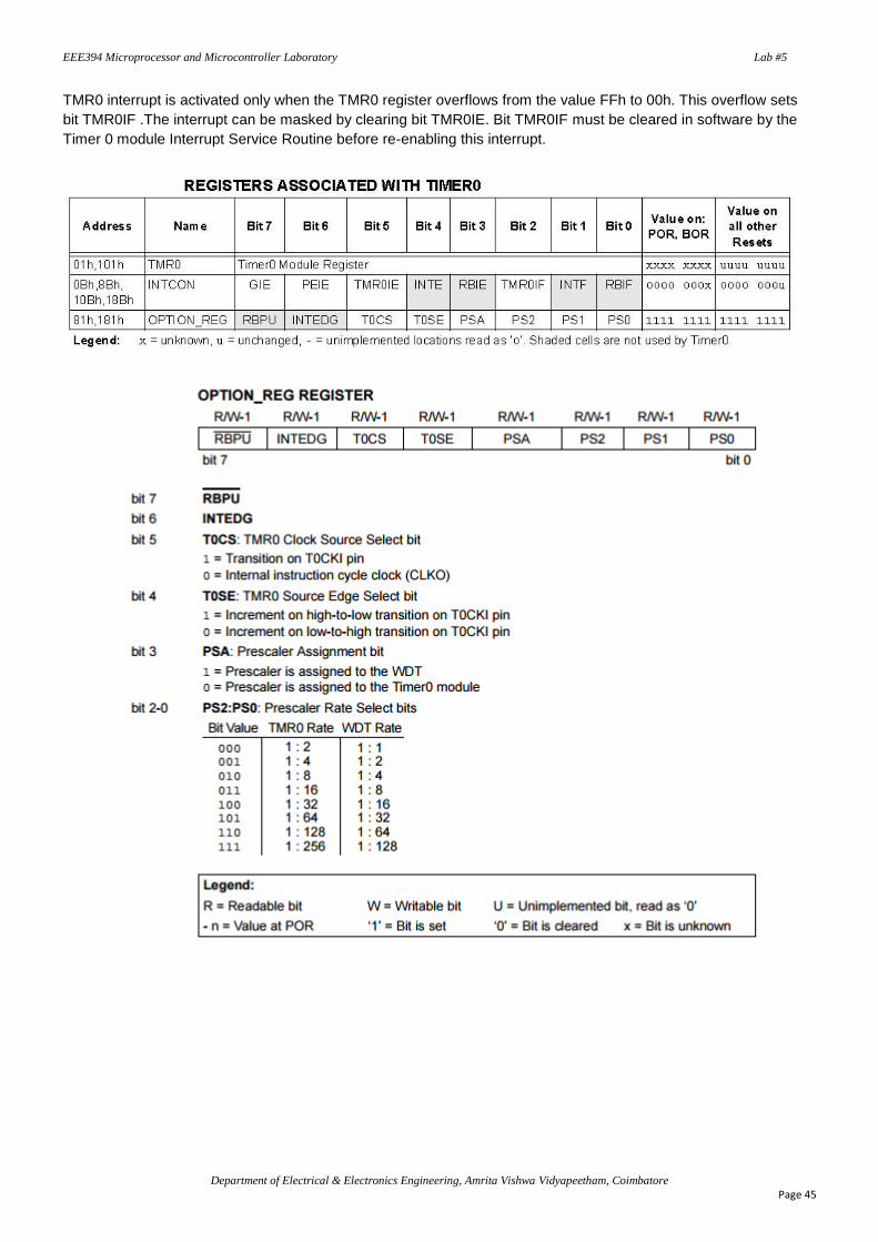
TMR0 interrupt is activated only when the TMR0 register overflows from the value FFh to 00h. This overflow sets
bit TMR0IF .The interrupt can be masked by clearing bit TMR0IE. Bit TMR0IF must be cleared in software by the
Timer 0 module Interrupt Service Routine before re-enabling this interrupt.
EEE394 Microprocessor and Microcontroller Laboratory Lab #5
Department of Electrical & Electronics Engineering, Amrita Vishwa Vidyapeetham, Coimbatore
Page 46
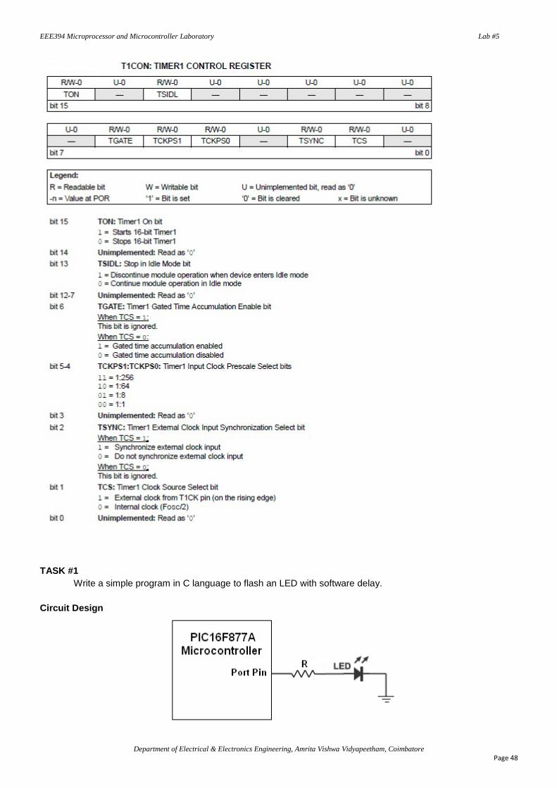
TIMER 1 MODULE
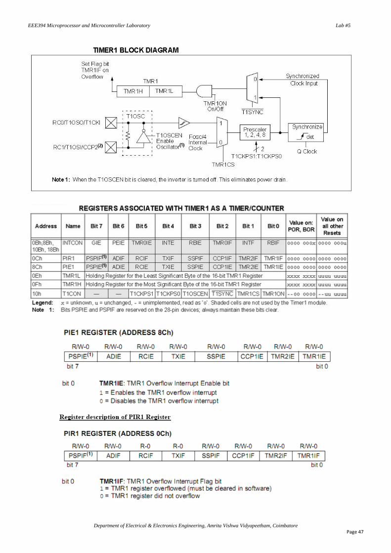
Timer 1 module is a 16 bit timer/counter unit. That is, it consists of two 8 bit (8+8) registers (TMR1H, TMR1L) which
read and write easily. TMR1 register is a pair of TMR1H and TMR1L and also its value increment its value from
0000h to FFFFh and rolls over to 0000h.
Timer 1 module basically operates in two different modes. They are
1) Timer mode
2) Counter mode
The operating mode of timer 1 module is selected by using the clock select bit (TMR1CS), in timer mode. The
Timer mode can be easily selected by clearing the TMR1CS bit. In this mode, the input clock to the timer is
FOSC/4. The synchronize control bit, T1SYNC, has no effect since the internal clock is always in sync. Timer1
Operation in Synchronized
Counter Mode
The synchronized Counter mode is selected by setting timer 1 synchronized counter select bit (TMR1CS). In this
mode, the timer increments on every rising edge of clock input on pin RC1/T1OSI/CCP2 when bit T1OSCEN is set,
or on pin RC0/T1OSO/T1CKI when bit T1OSCEN is cleared.
EEE394 Microprocessor and Microcontroller Laboratory Lab #5
Department of Electrical & Electronics Engineering, Amrita Vishwa Vidyapeetham, Coimbatore
Page 47
EEE394 Microprocessor and Microcontroller Laboratory Lab #5
Department of Electrical & Electronics Engineering, Amrita Vishwa Vidyapeetham, Coimbatore
Page 48
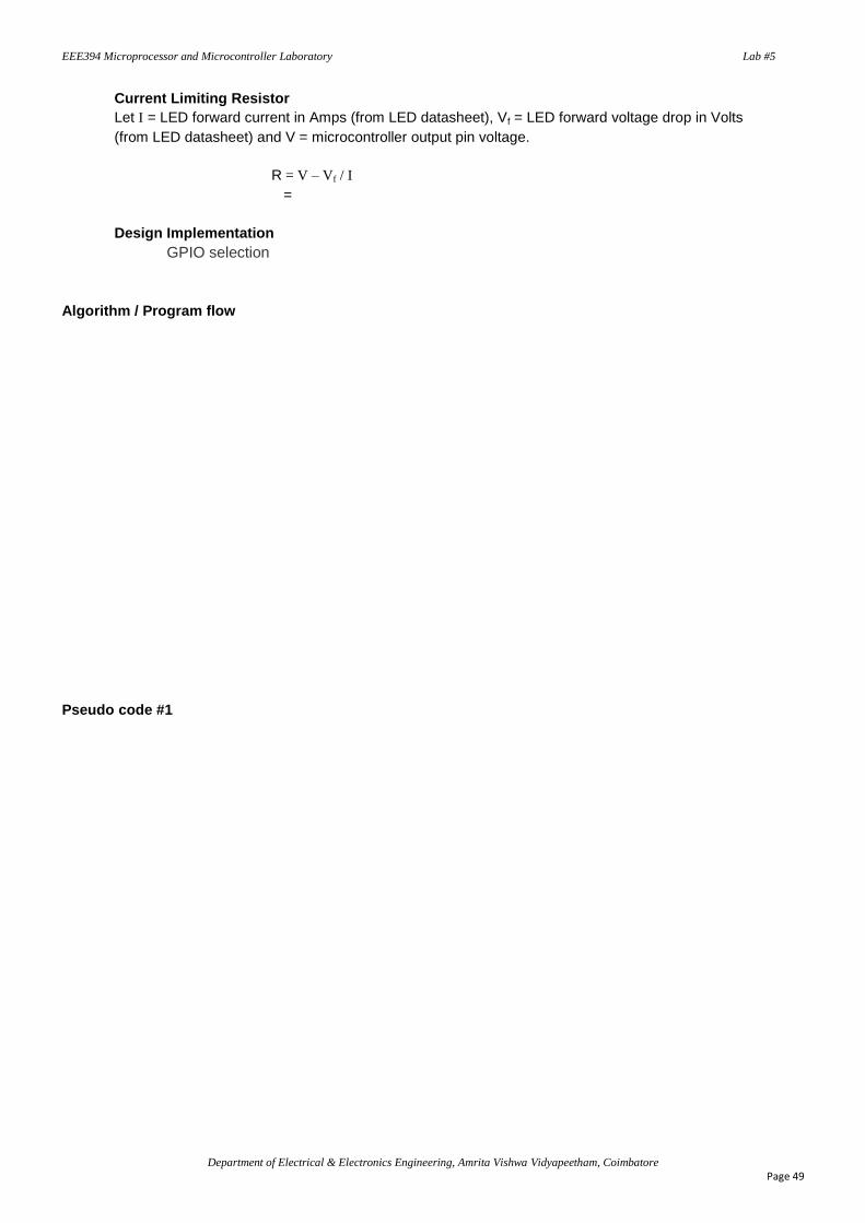
TASK #1
Write a simple program in C language to flash an LED with software delay.
Circuit Design
EEE394 Microprocessor and Microcontroller Laboratory Lab #5
Department of Electrical & Electronics Engineering, Amrita Vishwa Vidyapeetham, Coimbatore
Page 49
Current Limiting Resistor
Let I = LED forward current in Amps (from LED datasheet), Vf = LED forward voltage drop in Volts
(from LED datasheet) and V = microcontroller output pin voltage.
R = V – Vf / I
=
Design Implementation
GPIO selection
Algorithm / Program flow
Pseudo code #1
EEE394 Microprocessor and Microcontroller Laboratory Lab #5
Department of Electrical & Electronics Engineering, Amrita Vishwa Vidyapeetham, Coimbatore
Page 50
Source code #1
Testing and Verification
(i) Check the output using Logic Analyzer in MPLAB IDE
(ii) Implement the circuit in PROTEUS and verify the task.
Discussion & Inference
_____________________________________________________________________________________
_____________________________________________________________________________________
_____________________________________________________________________________________
_____________________________________________________________________________________
_____________________________________________________________________________________
_____________________________________________________________________________________
_____________________________________________________________________________________
EEE394 Microprocessor and Microcontroller Laboratory Lab #5
Department of Electrical & Electronics Engineering, Amrita Vishwa Vidyapeetham, Coimbatore
Page 51
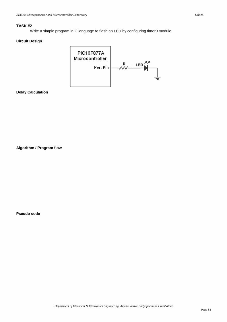
TASK #2
Write a simple program in C language to flash an LED by configuring timer0 module.
Circuit Design
Delay Calculation
Algorithm / Program flow
Pseudo code
EEE394 Microprocessor and Microcontroller Laboratory Lab #5
Department of Electrical & Electronics Engineering, Amrita Vishwa Vidyapeetham, Coimbatore
Page 52
Source code
Testing and Verification
Discussion & Inference
_____________________________________________________________________________________
_____________________________________________________________________________________
_____________________________________________________________________________________
_____________________________________________________________________________________
_____________________________________________________________________________________
_____________________________________________________________________________________
_____________________________________________________________________________________

EEE394 Microprocessor and Microcontroller Laboratory Lab #5
Department of Electrical & Electronics Engineering, Amrita Vishwa Vidyapeetham, Coimbatore
Page 53
TASK #3
Write a simple program in C language to flash an LED by configuring timer1 module.
Circuit Design
Delay Calculation
Pseudo code
EEE394 Microprocessor and Microcontroller Laboratory Lab #5
Department of Electrical & Electronics Engineering, Amrita Vishwa Vidyapeetham, Coimbatore
Page 54
Source code
Testing and Verification

EEE394 Microprocessor and Microcontroller Laboratory Lab #5
Department of Electrical & Electronics Engineering, Amrita Vishwa Vidyapeetham, Coimbatore
Page 55
Discussion & Inference
_____________________________________________________________________________________
_____________________________________________________________________________________
_____________________________________________________________________________________
_____________________________________________________________________________________
_____________________________________________________________________________________
_____________________________________________________________________________________
_____________________________________________________________________________________
EEE394 Microprocessor and Microcontroller Laboratory Lab #5
Department of Electrical & Electronics Engineering, Amrita Vishwa Vidyapeetham, Coimbatore
Page 56
UNDERSTANDING & LEARNING
_____________________________________________________________________________________
_____________________________________________________________________________________
_____________________________________________________________________________________
_____________________________________________________________________________________
_____________________________________________________________________________________
_____________________________________________________________________________________
_____________________________________________________________________________________
_____________________________________________________________________________________
_____________________________________________________________________________________
_____________________________________________________________________________________
_____________________________________________________________________________________
Prepared by:
Name: __________________________________________ Reg. No.: _________________________
Experiment Date: ……………
Report Submission Date: ……………
Submission Delay: …........
Signature
ASSESSMENT
Student Task Max.Marks Graded Marks
Pre-lab Preparation 10
Program flow / logic 10
Design / Implementation 10
Post-lab / Viva-voce 10
Total 40