Time-Saving and Cost-Effective Innovations for EMI Reduction
18
Yogesh Ramadass Distinguished Member Technical Staff Design Manager – Kilby Power, Isolation and Motors Texas Instruments Ambreesh Tripathi Member Group Technical Staff Systems Manager – Wide Input Buck Switching Regulators Texas Instruments Paul Curtis Analog Design Engineer Boost & Multi Channel/Phase DCDC Texas Instruments Time-Saving and Cost-Effective Innovations for EMI Reduction in Power Supplies
Transcript of Time-Saving and Cost-Effective Innovations for EMI Reduction

Yogesh RamadassDistinguished Member Technical Staff Design Manager – Kilby Power, Isolation and MotorsTexas Instruments
Ambreesh TripathiMember Group Technical StaffSystems Manager – Wide Input Buck Switching RegulatorsTexas Instruments
Paul CurtisAnalog Design Engineer Boost & Multi Channel/Phase DCDCTexas Instruments
Time-Saving and Cost-Effective Innovations for EMI Reduction in Power Supplies

2 April 2021Time-Saving and Cost-Effective Innovations for EMI Reduction in Power Supplies
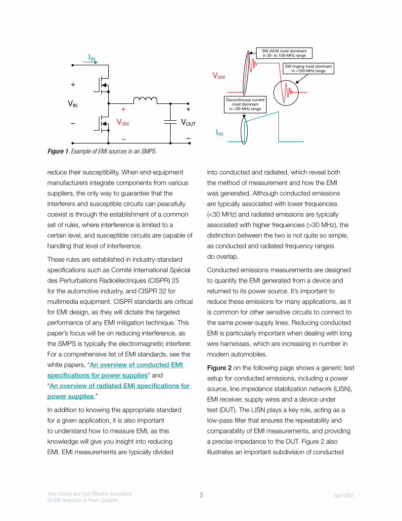
As electronic systems become increasingly dense and interconnected, reducing the effects of electromagnetic interference (EMI) becomes an increasingly critical system design consideration.
EMI can no longer be an afterthought, given its
potential to cause significant setbacks late in the
design phase that cost both time and money.
One of the most ubiquitous circuits in modern
technology is the switch-mode power supply
(SMPS), which provides drastic improvements in
efficiency over linear regulators in most applications.
But this efficiency comes at a price, as the switching
of power metal-oxide semiconductor field-effect
transistors (MOSFETs) in the SMPS causes it to
be a major source of EMI, which in turn can affect
reliability. EMI primarily comes from discontinuous
input currents, fast slew rates on switching nodes,
and additional ringing along switching edges caused
by parasitic inductances in the power loop.
Figure 1 on the following page illustrates how
each of these elements manifests itself in different
frequency bands, using a buck converter topology
as an example. As pressures mount to increase
switching frequencies for reduced size and cost,
as well as to increase slew rates for improved
efficiency, EMI problems are exacerbated. Thus, it’s
becoming necessary to incorporate cost-effective
and easily integrated EMI mitigation techniques that
do not compromise the power-supply design.
What is EMI?
In a system that requires electromagnetic
compatibility (EMC), components acting as
electromagnetic sources are designed to reduce
their interference, and components that are
susceptible to interference are designed to
What is EMI?
EMI is electromagnetic energy —
produced as an undesirable byproduct
of switching currents and voltages —
that comes from a variety of physical
phenomena and manifests during
stringent EMI tests.
Conventional methods to reduce EMI
Reducing EMI is an endeavor plagued
with trade-offs. Conventional methods
to reduce EMI include using large,
expensive filters or reducing switching
slew rates, a technique that directly
impacts efficiency.
Innovations in EMI reduction
To realize all of the benefits of a switch-
mode power supply, it is paramount
for EMI reduction techniques to resolve
the traditional trade-offs. This requires
creative solutions for both low- and
high-frequency EMI, as well as accurate
modeling techniques.
This paper examines EMI in switch-mode
power supplies, and provides technology
examples to help designers quickly and easily
pass industry-standard EMI tests.
At a glance
1
2
3
3 April 2021Time-Saving and Cost-Effective Innovations for EMI Reduction in Power Supplies
reduce their susceptibility. When end-equipment
manufacturers integrate components from various
suppliers, the only way to guarantee that the
interferers and susceptible circuits can peacefully
coexist is through the establishment of a common
set of rules, where interference is limited to a
certain level, and susceptible circuits are capable of
handling that level of interference.
These rules are established in industry-standard
specifications such as Comité International Spécial
des Perturbations Radioélectriques (CISPR) 25
for the automotive industry, and CISPR 32 for
multimedia equipment. CISPR standards are critical
for EMI design, as they will dictate the targeted
performance of any EMI mitigation technique. This
paper’s focus will be on reducing interference, as
the SMPS is typically the electromagnetic interferer.
For a comprehensive list of EMI standards, see the
white papers, “An overview of conducted EMI
specifications for power supplies” and
“An overview of radiated EMI specifications for
power supplies.”
In addition to knowing the appropriate standard
for a given application, it is also important
to understand how to measure EMI, as this
knowledge will give you insight into reducing
EMI. EMI measurements are typically divided
into conducted and radiated, which reveal both
the method of measurement and how the EMI
was generated. Although conducted emissions
are typically associated with lower frequencies
(<30 MHz) and radiated emissions are typically
associated with higher frequencies (>30 MHz), the
distinction between the two is not quite so simple,
as conducted and radiated frequency ranges
do overlap.
Conducted emissions measurements are designed
to quantify the EMI generated from a device and
returned to its power source. It’s important to
reduce these emissions for many applications, as it
is common for other sensitive circuits to connect to
the same power-supply lines. Reducing conducted
EMI is particularly important when dealing with long
wire harnesses, which are increasing in number in
modern automobiles.
Figure 2 on the following page shows a generic test
setup for conducted emissions, including a power
source, line impedance stabilization network (LISN),
EMI receiver, supply wires and a device under
test (DUT). The LISN plays a key role, acting as a
low-pass filter that ensures the repeatability and
comparability of EMI measurements, and providing
a precise impedance to the DUT. Figure 2 also
illustrates an important subdivision of conducted
Figure 1. Example of EMI sources in an SMPS.
VIN
+
– VOUT
Discontinuous currentmost dominant
in <30-MHz range
SW ringing most dominantin >100-MHz range
SW dV/dt most dominantin 30- to 100-MHz range
+
–
V
V
SW
SW
+
–
I
I
IN
IN

4 April 2021Time-Saving and Cost-Effective Innovations for EMI Reduction in Power Supplies
emissions into common-mode (CM) and differ-
ential-mode (DM) currents. DM currents flow
between the power-supply line and its return path,
and are the dominant factor at lower frequencies.
CM currents flow between each of the power
lines and ground, and are the dominant factor at
higher frequencies.
Radiated measurements have a setup similar to
conducted measurements; the main difference is
that the EMI receiver is not connected directly to
the LISN but to a nearby antenna. Radiated energy
in an SMPS comes from fast transient current
loops generating magnetic fields, and fast transient
voltage surfaces generating electric fields. Because
the same current loops that generate radiated
magnetic fields also generate DM conducted
emissions, and the same surfaces that generate
radiated electric fields also generate CM conducted
emissions, many EMI mitigation techniques reduce
both conducted and radiated emissions, but may
be targeted specifically for one or the other.
In general, lower-frequency emissions are mitigated
by using large passive filters, which add board
area and cost to the solution. High-frequency
emissions present different challenges in terms of
measurement, modeling and mitigation, primarily
as a result of their parasitic nature. Common
mitigation techniques for high-frequency emissions
include controlling slew rates and reducing
parasitics. Figure 3 summarizes the mitigation
techniques contained in this paper, the frequency
bands in which they are most beneficial and an
example of the frequency ranges covered by the
CISPR 25 standard.
Conventional methods to reduce EMI in the low- and high-frequency ranges
Input voltage ripple generated by discontinuous
currents in an SMPS can conduct to other systems
when the systems share common physical
Figure 3. A summary of the EMI mitigation techniques presented in this paper.
Figure 2. Generic test setup for conducted emissions
measurements, with DM and CM loops highlighted in teal and
red, respectively.
LoadDM loop area
CM loop area
VCM
+
—
iDM
+– VDM
Reference GND plane
VIN
iDM
iCM
iCM /2
iCM /2
DC/DC
regulator
( DUT)
VIN+
VIN–
V
V
OUT+
OUT–
LISN
EMI
receiver
LISN
V1
V2
V1 + V2=
2
++
–
1kHz
30MHz
108MHz MHz
200 1GHz
Conducted
Very low frequency
Conducted
CISPR 25 low frequency
Conducted
CISPR 25 high frequency
Radiated
CISPR 25 rod antenna
Radiated
CISPR 25 log antenna
Radiated
CISPR 25 bicon antenna
Spread spectrum
Slew rate control
Active EMI filtering
Package optimization
EMI modeling flows
Cancellation windings
Integrated capacitors
150kHz
5 April 2021Time-Saving and Cost-Effective Innovations for EMI Reduction in Power Supplies
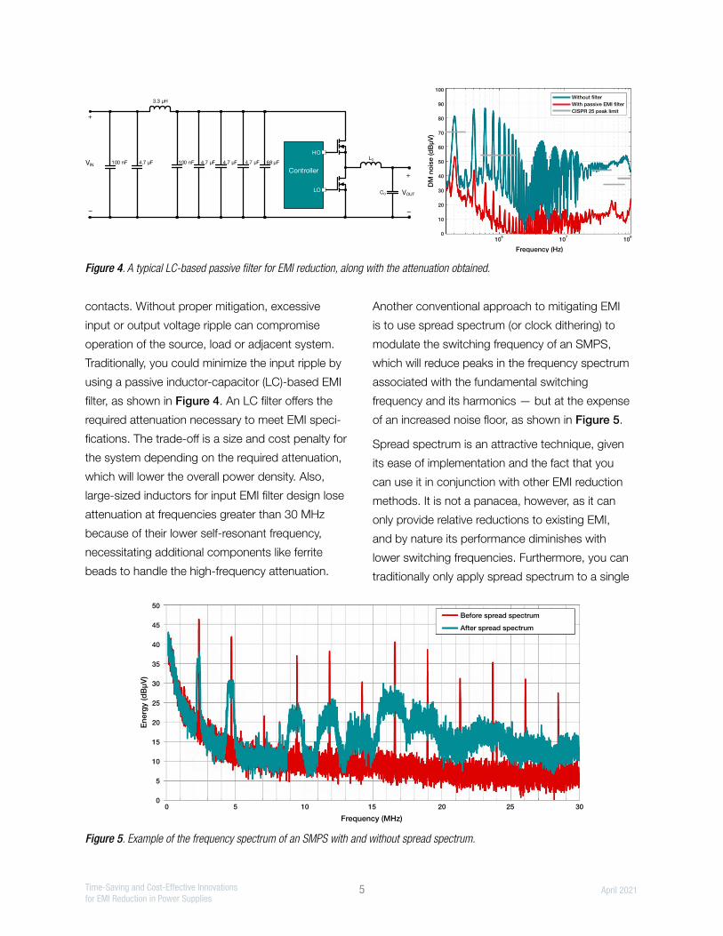
contacts. Without proper mitigation, excessive
input or output voltage ripple can compromise
operation of the source, load or adjacent system.
Traditionally, you could minimize the input ripple by
using a passive inductor-capacitor (LC)-based EMI
filter, as shown in Figure 4. An LC filter offers the
required attenuation necessary to meet EMI speci-
fications. The trade-off is a size and cost penalty for
the system depending on the required attenuation,
which will lower the overall power density. Also,
large-sized inductors for input EMI filter design lose
attenuation at frequencies greater than 30 MHz
because of their lower self-resonant frequency,
necessitating additional components like ferrite
beads to handle the high-frequency attenuation.
Another conventional approach to mitigating EMI
is to use spread spectrum (or clock dithering) to
modulate the switching frequency of an SMPS,
which will reduce peaks in the frequency spectrum
associated with the fundamental switching
frequency and its harmonics — but at the expense
of an increased noise floor, as shown in Figure 5.
Spread spectrum is an attractive technique, given
its ease of implementation and the fact that you
can use it in conjunction with other EMI reduction
methods. It is not a panacea, however, as it can
only provide relative reductions to existing EMI,
and by nature its performance diminishes with
lower switching frequencies. Furthermore, you can
traditionally only apply spread spectrum to a single
VOUT
+
–
Controller
HO
LO
LO
CO
68 µF4.7 µF4.7 µF4.7 µF100 nFVIN
+
–
3.3 µH
4.7 µF100 nF
DM
no
ise (d
Bµ
V)
Frequency (Hz)
100
90
80
70
60
50
40
30
20
10
010
610
710
8
Without filter
With passive EMI filter
CISPR 25 peak limit
Figure 4. A typical LC-based passive filter for EMI reduction, along with the attenuation obtained.
50
45
40
35
30
25
20
15
10
5
00 5 10 15 20 25
En
erg
y (d
Bµ
V)
Frequency (MHz)
Before spread spectrum
After spread spectrum
30
Figure 5. Example of the frequency spectrum of an SMPS with and without spread spectrum.

6 April 2021Time-Saving and Cost-Effective Innovations for EMI Reduction in Power Supplies
frequency band, for reasons that we will explore in
the next section.
To minimize the size of the filter inductors, you
can choose higher switching frequencies for your
SMPS design. It is important to avoid sensitive
frequency bands for switcher operation, however.
For example, the preferred switching frequency for
automotive power solutions has traditionally been
in the sub-AM bands (approximately 400 kHz).
Choosing a higher switching frequency to minimize
inductor size means that you must avoid the entire
AM band (525 to 1,705 kHz) so as to not have
fundamental switching spurs in the more stringent
automotive EMI frequency bands.
Switching converters from Texas Instruments (TI)
have a switching frequency above 1.8 MHz to
satisfy the EMI band requirements. The push to
higher switching frequencies imposes a severe
restriction on the switching transition rise and fall
times to reduce switching losses. However, a switch
node with very short rise and fall times maintains
high energy content even at high frequencies close
to its 100th harmonic, as shown in Figure 6, again
highlighting the trade-off between high efficiency
and low EMI.
High slew rates will additionally result in
high-frequency switch-node ringing, due to the
presence of parasitic inductances in the power
path of DC/DC converters, which further increases
emissions at the ringing frequency and above.
Figure 7 on the following page shows how the
slew rate and the associated ringing on the switch
node affect emissions. The traditional way to limit
EMI emissions caused by the switching transition
is to slow them down by adding intentional
resistance in the gate-drive path of the switching
device. This causes the transitions to happen more
slowly, leading to faster roll-off of the emissions
and an 8- to 10-dB reduction in emissions at
the ringing frequency. This slowdown of the
switching edges comes with a penalty of 2% to
3% in the peak current efficiency of the switching
converter, however.
Innovations in reducing low-frequency emissions
Let’s look at a few techniques that TI uses when
building its converters and controllers to address the
fundamental trade-offs involving efficiency, EMI, size
and cost.
Sp
ec
tru
m /
dB
Frequency / Hz
500k 800k 1M 2M2M1.5M 2.5M650k
Light red: 1-ns rise time
Dark red: 40-ns rise time
�
>20 dB
100 MHz / div
–20
–40
–60
–80
–100
–120
3M 4M 5M 6M 7M 8M 10M 15M 25M20M 30M 40M 50M 60M 80M 100M 200M 400M 600M 1G800M250M150M
Figure 6. EMI plots of square waveforms with different rise times.

7 April 2021Time-Saving and Cost-Effective Innovations for EMI Reduction in Power Supplies
Spread spectrum
Spread spectrum uses the principle of conservation
of energy to reduce EMI peaks by spreading energy
across multiple frequencies. However, the peak
energy that a susceptible circuit “sees” may not
reduce; it depends on the relationship between the
susceptible circuit’s bandwidth and the method
of frequency modulation. When measuring EMI,
the spectrum analyzer is acting as the susceptible
circuit, and industry standards set the resolution
bandwidth (RBW). Thus, it is important to modulate
the frequency in the most effective way for the
standard you are targeting. A general rule of
thumb is to have the modulation frequency, fm,
approximately equal to your targeted RBW, with the
spreading bandwidth, ΔfC, around ±5% to ±10%.
Figure 8 illustrates these parameters in both the
time and frequency domains.
It is common to set fm around 9 kHz to optimize for
the low-frequency band in standards such as CISPR
25, but this happens to also be in the audible
range. To combat this, you can further modulate
the triangular modulation in a pseudorandom
fashion to spread the audible energy without
having a significant impact on the conducted
and radiated EMI performance. Figure 9 on the
following page illustrates this modulation profile both
in the time and the frequency domains, a feature
present on the TPS55165-Q1, a synchronous
buck-boost converter.
The fact that EMI is not limited to a single band (and
thus a single RBW) but multiple bands presents
a predicament, as spread spectrum can typically
only target improvements in a single band. A new
solution to this problem is a digital spread-spectrum
technique called dual random spread spectrum
(DRSS). The basic principle behind DRSS is
to superimpose two modulation profiles, each
V (V
)
dB
Time (µs)
13.0
12.0
11.0
10.0
9.0
8.0
7.0
6.0
5.0
4.0
3.0
2.0
1.0
0.0
20.0
10.0
0.0
–10.0
–20.0
–30.0
–40.0
–50.0
–60.0
–70.0
–80.0
1.005 1.015 1.0251.01 1.02
SW (RB = 0 )
SW (RB = 500 )
�
�
Slew rate
3.8 V/ns Slew rate
1.6 V/ns
106
107
108
109
Hz
FFT of SW node
~10 dB @
160 MHz
�
~8 dB @
400 MHz
�
Figure 7. The effect of different switch-node slew rates and associated ringing on high-frequency emissions. Reduced slew rates
impact EMI roll-off in the 30- to 200-MHz band while the reduced ringing impacts EMI at the ringing frequency around 400 MHz.
fm
Time
Clock frequency
fc
fc
�fc
2 f� c
Tm =1fm
Frequency
Energy
Unmodulated
Modulated
Figure 8. Spread-spectrum parameters fm and ΔfC in both the time and
frequency domains.
8 April 2021Time-Saving and Cost-Effective Innovations for EMI Reduction in Power Supplies
targeting a different RBW. For more information,
see the application report, “EMI Reduction
Technique, Dual Random Spread Spectrum.”
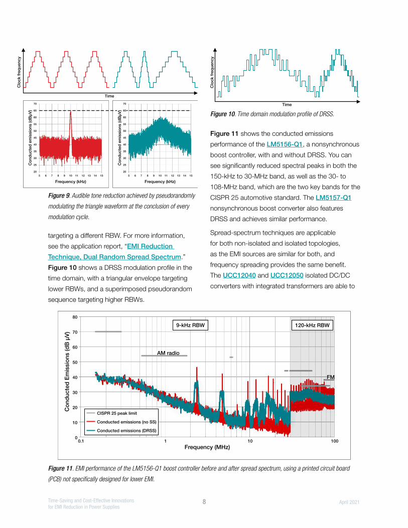
Figure 10 shows a DRSS modulation profile in the
time domain, with a triangular envelope targeting
lower RBWs, and a superimposed pseudorandom
sequence targeting higher RBWs.
Figure 11 shows the conducted emissions
performance of the LM5156-Q1, a nonsynchronous
boost controller, with and without DRSS. You can
see significantly reduced spectral peaks in both the
150-kHz to 30-MHz band, as well as the 30- to
108-MHz band, which are the two key bands for the
CISPR 25 automotive standard. The LM5157-Q1
nonsynchronous boost converter also features
DRSS and achieves similar performance.
Spread-spectrum techniques are applicable
for both non-isolated and isolated topologies,
as the EMI sources are similar for both, and
frequency spreading provides the same benefit.
The UCC12040 and UCC12050 isolated DC/DC
converters with integrated transformers are able to
Co
nd
ucte
d e
mis
sio
ns (d
Bµ
V)
70
65
60
55
50
45
40
35
30
25
20
Co
nd
ucte
d e
mis
sio
ns (d
Bµ
V)
70
65
60
55
50
45
40
35
30
25
20
Frequency (kHz)
5 6 7 8 9 10 11 12 13 14 15
Frequency (kHz)
Time
5 6 7 8 9 10 11 12 13 14 15
Clo
ck f
req
uen
cy
Figure 9. Audible tone reduction achieved by pseudorandomly
modulating the triangle waveform at the conclusion of every
modulation cycle.C
lock f
req
uen
cy
Time
Figure 10. Time domain modulation profile of DRSS.
Co
nd
uc
ted
Em
issio
ns (
dB
µV
)
80
70
60
50
40
30
20
10
0
CISPR 25 peak limit
Conducted emissions (no SS)
Conducted emissions (DRSS)
9-kHz RBW 120-kHz RBW
FM
AM radio
Frequency (MHz)0.1 1 10 100
Figure 11. EMI performance of the LM5156-Q1 boost controller before and after spread spectrum, using a printed circuit board
(PCB) not specifically designed for lower EMI.

9 April 2021Time-Saving and Cost-Effective Innovations for EMI Reduction in Power Supplies
pass CISPR 32 Class B EMI testing limits in part
due to internal spread-spectrum techniques.
Active EMI filtering
To substantially improve emissions in the
low-frequency spectrum, the LM25149-Q1 buck
controller incorporates an active EMI filtering
approach. The integrated active EMI filter reduces
DM conducted emissions at the input by acting as
an effective low-impedance shunt. Figure 12 shows
how the active EMI filter of the buck controller
connects to the input line. The sense and inject
pins hook up to the input through their respective
capacitors. The active element within the active
EMI filter block amplifies the sensed signal and
injects an appropriate anti-polarity signal through
the inject capacitor in order to minimize the overall
disturbance on the input line. This reduces the
filtering burden on the passive elements needed,
thereby reducing their size, volume and cost.
Figure 13 shows the EMI measurement results of
a buck converter operating at a 400-kHz switching
frequency, comparing the active and passive EMI
filtering approaches. To effectively meet the CISPR
25 Class 5 spectral mask, the passive EMI filter
needs a 3.3-µH DM inductor with a 10-µF DM
capacitor. The active filtering approach can achieve
the same effective attenuation with a DM inductor
of only 1 µH along with 100-nF sense and inject
capacitors. This helps reduce the size and volume
of the passive filter to about 43% and 27% of the
original values, respectively. For higher-current
converters, it is possible to obtain further benefits
in cost and efficiency from a reduction in inductor
DC resistance.
Cancellation windings
Unlike non-isolated converters, an additional
emissions path across the isolation boundary is a
key cause of common-mode (CM) EMI in isolated
converters. Figure 14 on the following page shows
the presence of the parasitic capacitances across
the isolation transformer in a standard flyback
converter. CM currents can flow directly from
primary to earth through the parasitic capacitance
associated with each switched node. The CM
currents also flow from primary to secondary
because of parasitic capacitance between the
windings, causing an increase in the measured
VIN
+
–
VOUT
+
–
INJ
SEN
AGND
Controller
+
AEF
HO
LORcomp1
Ccomp1
Csen Cinj
L
LO
CO
Cin
Ccomp Rcomp
RDC_fb
Figure 12. Active EMI filter showing the sense, inject capacitors
and components for compensation.
DM
no
ise
(d
Bµ
V)
100
90
80
70
60
50
40
30
20
10
010
610
710
8
Frequency (Hz)
3.3-µH DM inductor
with traditional
passive EMI filter
1-µH DM inductor
with AEF
Bare noise
With passive EMI filter
With AEF
CISPR 25 peak limit
Figure 13. EMI attenuation obtained using passive and active
filtering and comparison of the passive inductor needed for
filtering in both approaches for a 12-V input, 5-V/5-A output
buck converter.

10 April 2021Time-Saving and Cost-Effective Innovations for EMI Reduction in Power Supplies
CM EMI. Conventionally, you could attenuate this
additional disturbance by using a large CM choke in
the input power path.
To help minimize the size of the passive filtering,
the 65-W active clamp flyback with silicon FETs
reference design for a high-power-density
5- to 20-V AC/DC adapter employs cancellation
winding- and shielding-based approaches specific
to isolated converters. As shown in Figure 15, an
improved internal transformer structure has an extra
auxiliary winding layer (shown in black) inserted in
between the inner primary and secondary layers
for CM balance. The auxiliary CM balance layer
shields the inner half-primary to secondary interface
and helps generate a canceling CM voltage to
null the CM injection from the outer half-primary
layer. Equalizing the parasitic capacitances to the
secondary layer from the auxiliary winding and
primary outer layers helps null the CM current
injected into the secondary layer from the outer
half-primary layer, by pushing an opposite-phase
CM current from the cancellation layer. The net
effect — close to zero CM current flowing into
the secondary layer — reduces CM emissions,
significantly helping the design meet EMI spectral
standards with minimal CM filtering.
Innovations in reducing high-frequency emissions
The EMI mitigation techniques we’ve described
so far generally reduce low-frequency emissions
(<30 MHz), with a corresponding reduction in the
amount of passive filtering required and associated
size, volume and cost benefits. Now, let’s look at
techniques designed to mitigate high-frequency
emissions (>30 MHz).
Earth
V
CM EMIvoltage
AC
+
–
Z
Figure 14. CM EMI generating parasitics in a flyback converter.
Primary(outer layer)
Auxiliary bias
CM balanceauxiliary
Secondary
Primary(inner layer)
NP NS NAUX
CP–SP–S CS-AUX
ICM1 ICM2
100
90
80
70
60
50
40
30
20
10
0
EN55032 QP 8
EN55032 AV-8
QP result
AVG result
-
115 V – Conducted EMI QP and AVG with earthed loaddBµV
MHz1010.1
Figure 15. Using shielding and cancellation windings to reduce EMI in a flyback converter.
11 April 2021Time-Saving and Cost-Effective Innovations for EMI Reduction in Power Supplies
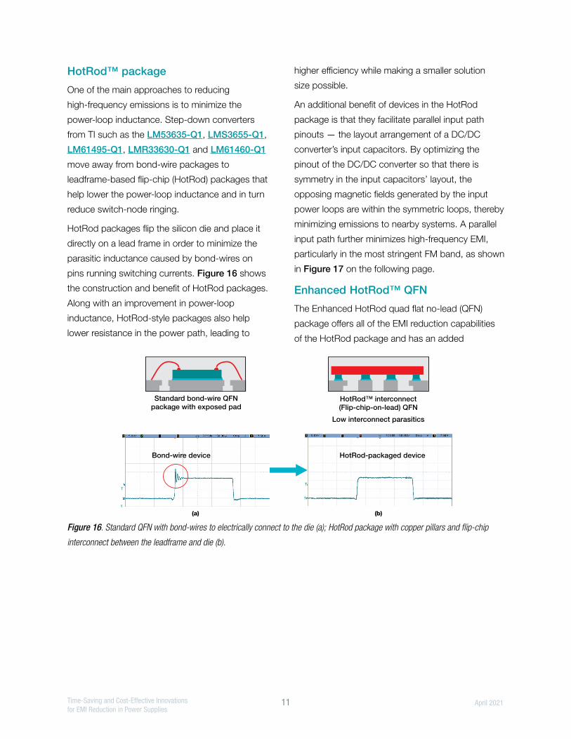
HotRod™ package
One of the main approaches to reducing
high-frequency emissions is to minimize the
power-loop inductance. Step-down converters
from TI such as the LM53635-Q1, LMS3655-Q1,
LM61495-Q1, LMR33630-Q1 and LM61460-Q1
move away from bond-wire packages to
leadframe-based flip-chip (HotRod) packages that
help lower the power-loop inductance and in turn
reduce switch-node ringing.
HotRod packages flip the silicon die and place it
directly on a lead frame in order to minimize the
parasitic inductance caused by bond-wires on
pins running switching currents. Figure 16 shows
the construction and benefit of HotRod packages.
Along with an improvement in power-loop
inductance, HotRod-style packages also help
lower resistance in the power path, leading to
higher efficiency while making a smaller solution
size possible.
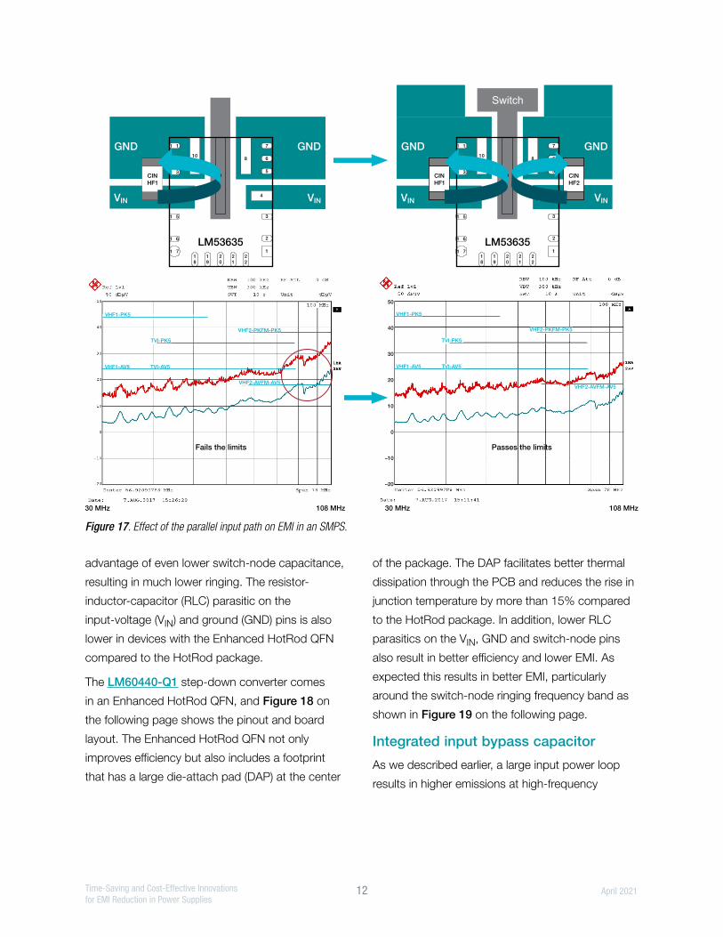
An additional benefit of devices in the HotRod
package is that they facilitate parallel input path
pinouts — the layout arrangement of a DC/DC
converter’s input capacitors. By optimizing the
pinout of the DC/DC converter so that there is
symmetry in the input capacitors’ layout, the
opposing magnetic fields generated by the input
power loops are within the symmetric loops, thereby
minimizing emissions to nearby systems. A parallel
input path further minimizes high-frequency EMI,
particularly in the most stringent FM band, as shown
in Figure 17 on the following page.
Enhanced HotRod™ QFN
The Enhanced HotRod quad flat no-lead (QFN)
package offers all of the EMI reduction capabilities
of the HotRod package and has an added
Bond-wire device HotRod-packaged device
Standard bond-wire QFN
package with exposed padHotRod™ interconnect
(Flip-chip-on-lead) QFN
Low interconnect parasitics
T
1
T
1
(a) (b)
Figure 16. Standard QFN with bond-wires to electrically connect to the die (a); HotRod package with copper pillars and flip-chip
interconnect between the leadframe and die (b).
12 April 2021Time-Saving and Cost-Effective Innovations for EMI Reduction in Power Supplies
advantage of even lower switch-node capacitance,
resulting in much lower ringing. The resistor-
inductor-capacitor (RLC) parasitic on the
input-voltage (VIN) and ground (GND) pins is also
lower in devices with the Enhanced HotRod QFN
compared to the HotRod package.
The LM60440-Q1 step-down converter comes
in an Enhanced HotRod QFN, and Figure 18 on
the following page shows the pinout and board
layout. The Enhanced HotRod QFN not only
improves efficiency but also includes a footprint
that has a large die-attach pad (DAP) at the center
of the package. The DAP facilitates better thermal
dissipation through the PCB and reduces the rise in
junction temperature by more than 15% compared
to the HotRod package. In addition, lower RLC
parasitics on the VIN, GND and switch-node pins
also result in better efficiency and lower EMI. As
expected this results in better EMI, particularly
around the switch-node ringing frequency band as
shown in Figure 19 on the following page.
Integrated input bypass capacitor
As we described earlier, a large input power loop
results in higher emissions at high-frequency
30 MHz 108 MHz
VHF1-AV5 TVI-AV5
50
40
30
20
10
0
–10
–20
TVI-PK5
VHF2-AVFM-AV5
VHF2-PKFM-PK5
VHF1-PK5
1 2
3
21 6
1 5
1
8
1
9
2
0
2
1
2
2
810
414
11 7
VIN VIN
CIN
HF1
CIN
HF2
GNDGND
LM53635
6
5
71 1
1 39
Switch
30 MHz 108 MHz
Fails the limits Passes the limits
VHF2-PKFM-PK5
VHF1-AV5
VHF1-PK5
TVI-AV5
TVI-PK5
VHF2-AVFM-AV5
1 2
3
21 6
1 5
1
8
1
9
2
0
2
1
2
2
810
414
11 7
VIN VIN
CIN
HF1
GNDGND
LM53635
6
5
71 1
1 39
Figure 17. Effect of the parallel input path on EMI in an SMPS.

13 April 2021Time-Saving and Cost-Effective Innovations for EMI Reduction in Power Supplies
bands because of increased switch-node ringing.
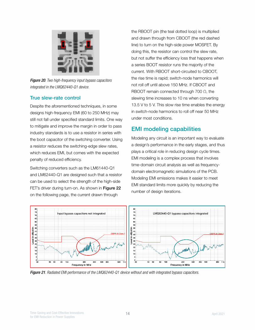
Integrating high-frequency input decoupling
capacitors inside the device package helps minimize
the input loop parasitic and thus reduces EMI.
This technique is used in the LMQ62440-Q1, a
step-down converter, as shown in Figure 20 on
the following page. Beyond reducing the input
power-loop inductance, the package integration of
the input high-frequency capacitors also helps make
the solution more immune to changes in the board
layout of the end system.
Figure 21 on the following page compares the
radiated EMI — identical conditions on identical
boards — of the LMQ62440-Q1, with and without
the bypass capacitors integrated. The results show
a 9-dB reduction in emission in the most stringent
TV band (200 to 230 MHz), which helps the system
remain under EMI limits set by industry standards
without the need for additional components on
the board.
12
2
3
4
76
10
9
8
13
SW
VIN
EN
PG
FB
AGND
VCC
BOOT
SW
VIN
DAP
12
5
SW
PGND
VINVIN 102
11
LIND
VOUT
The boot and VCC capslocate as close as possibleto the IC pins, resulting inlow parasitic inductancefor the MOSFET gate loops.
Input caps located closeto IC pins and in butterflyarrangement for H-fieldcancellation.
Butterfly arrangement ofoutput caps minimizeseffective loop inductancethrough H-fieldcancellation.
L1L2
121
2
3
4
5 76
11
10
9
8
13
SW
PGND
VIN
EN
PG
FB
AGND
VCC
BOOT
SW
VIN
DAP
PGND
LM604x0 pin-out
LM604x0 layout with parallel input loops
Shielded inductor withterminations underneaththe package.
PGND1
Figure 18. The pinout and PCB layout on an Enhanced HotRod™ QFN package device.
–10.0
–20.0
–30.0
–40.0
–50.0
–60.0
spectrum_SW
spectrum_SW
MHz
dB
Red: HotRod™ package
Teal: Enhanced HotRod™ package
100 400 1,000500
Figure 19. SW node FFT comparison of HotRod- vs. Enhanced HotRod-packaged device.
14 April 2021Time-Saving and Cost-Effective Innovations for EMI Reduction in Power Supplies
True slew-rate control
Despite the aforementioned techniques, in some
designs high-frequency EMI (60 to 250 MHz) may
still not fall under specified standard limits. One way
to mitigate and improve the margin in order to pass
industry standards is to use a resistor in series with
the boot capacitor of the switching converter. Using
a resistor reduces the switching-edge slew rates,
which reduces EMI, but comes with the expected
penalty of reduced efficiency.
Switching converters such as the LM61440-Q1
and LM62440-Q1 are designed such that a resistor
can be used to select the strength of the high-side
FET’s driver during turn-on. As shown in Figure 22
on the following page, the current drawn through
the RBOOT pin (the teal dotted loop) is multiplied
and drawn through from CBOOT (the red dashed
line) to turn on the high-side power MOSFET. By
doing this, the resistor can control the slew rate,
but not suffer the efficiency loss that happens when
a series BOOT resistor runs the majority of the
current. With RBOOT short-circuited to CBOOT,
the rise time is rapid; switch-node harmonics will
not roll off until above 150 MHz. If CBOOT and
RBOOT remain connected through 700 Ω, the
slewing time increases to 10 ns when converting
13.5 V to 5 V. This slow rise time enables the energy
in switch-node harmonics to roll off near 50 MHz
under most conditions.
EMI modeling capabilities
Modeling any circuit is an important way to evaluate
a design’s performance in the early stages, and thus
plays a critical role in reducing design cycle times.
EMI modeling is a complex process that involves
time-domain circuit analysis as well as frequency-
domain electromagnetic simulations of the PCB.
Modeling EMI emissions makes it easier to meet
EMI standard limits more quickly by reducing the
number of design iterations.
Figure 20. Two high-frequency input bypass capacitors
integrated in the LMQ62440-Q1 device.
Figure 21. Radiated EMI performance of the LMQ62440-Q1 device without and with integrated bypass capacitors.

15 April 2021Time-Saving and Cost-Effective Innovations for EMI Reduction in Power Supplies
Let’s review some of the options available to you for
modeling EMI.
Low-frequency EMI designs using WEBENCH® design tool
The WEBENCH input filter design tool helps you
automatically design a proper input filter to mitigate
lower-frequency (<30 MHz) conducted EMI noise for
compliance standards like CISPR 32 and CISPR 25.
The tool optimizes filter size while ensuring that the
design complies with a particular standard. It also
ensures filter stability and converter-loop stability
while designing the filter. This online tool supports
over 100 TI power devices.
It’s a common mistake to leave an input EMI filter
inductor undamped, which negatively affects
overall design stability. The WEBENCH design tool
performs impedance analysis on the input filter
and SMPS (as shown in Figure 23 on the following
page) and suggests the appropriate damping
component to ensure stability.
(a)
(b)
CBOOT
SW
RBOOT
VCC
VIN
LM62440-Q1
HS FET
LS FET
HS
driver
Figure 22. True slew-rate control implementation in the LM62440 (a); reduction in switch-node ringing using true slew-rate control (b).

16 April 2021Time-Saving and Cost-Effective Innovations for EMI Reduction in Power Supplies
Conducted and radiated EMI results published in data sheets
SMPS device evaluation modules are tested
against most stringent industrial and automotive
EMI standards, and results are published in
the data sheet to help you understand the EMI
performance of the devices in advance. You can
access a detailed EMI report by clicking “Optimized
for Ultra-Low EMI Requirements” on the first
page of the device data sheet. The EMI report in
the LM62440-Q1 data sheet includes complete
data for a CISPR 25 Class 5 conducted and
radiated setup.
In addition, TI can perform system-level EMI
modeling and measurements in-house to help
you validate EMI performance and accelerate
cycle times.
Ripple frequency spectrum (before filter)
Filter
V
Rz Lz Lf_inpflt
Cf_inpflt
Cb_inpflt
Rd_inpflt
Powersupply
Filter components
Lf 1 µ H
Cf 7.8 µ F
Cb 4 µ F
Rd 100 m �
1 µH511.4 m� 1 µH190 m�
1 µF5
Qty = 4�
100 m�
10 µF1 m
Qty = 2�
IN
Line impedance
+
–
120
100
80
60
40
20
Frequency (kHz)
Rip
ple
mag
nit
ud
e (d
Bµ
V)
Ripple magnitude (before filter)
CISPR 25 Class 5 noise limit
5 10 15 20 250
1
60
40
20
0
–20100
Filter output impedance
Converter input impedance open loop
Converter input impedance ideal loop
10 k 1 M
Frequency (Hz)
Gain
(d
B)
Filter vs. converter impedance comparison
Ripple frequency spectrum (after filter)
80
60
40
20
0
Ripple magnitude (after filter)
CISPR 25 Class 5 noise limit
Frequency (kHz)
5 10 15 20 250
Rip
ple
mag
nit
ud
e (d
Bµ
V)
Figure 23. Input EMI suggestion with impedance analysis in the WEBENCH® design tool.

Conclusion
The rapid growth of electronics has put tremendous
strain on the design of power converters, where
complex systems are crammed into ever-smaller
spaces. The close proximity of sensitive systems
makes it challenging to suppress EMI. You must
take extreme care when designing power converters
to comply with the limits set forth by standards
bodies to ensure that critical systems can operate
safely in a noisy environment.
Designing for low EMI can save you significant
development cycle time while also reducing
board area and solution cost. TI offers multiple
features and technologies to mitigate EMI such as
spread spectrum, active EMI filtering, cancellation
windings, package innovations, integrated
input bypass capacitors, and true slew-rate
control methodologies.
Employing a combination of techniques with TI’s
EMI-optimized power-management devices ensures
that designs using TI components will pass industry
standards without much rework. TI products enable
you to remain under end-equipment EMI limits
without sacrificing power density or efficiency.
See ti.com/lowemi to learn more about TI products
that use these technologies, including buck-boost
and inverting regulators, isolated bias supplies,
multichannel integrated circuits (PMIC), step-down
(buck) regulators and step-up (boost) regulators.
Key product categories for low EMI
Buck-boost & inverting regulators
Isolated bias supplies
Multi-channel ICs (PMIC)
Step-down (buck) regulators
Step-up (boost) regulators
Important Notice: The products and services of Texas Instruments Incorporated and its subsidiaries described herein are sold subject to TI’s standard terms and conditions of sale. Customers are advised to obtain the most current and complete information about TI products and services before placing orders. TI assumes no liability for applications assistance, customer’s applications or product designs, software performance, or infringement of patents. The publication of information regarding any other company’s products or services does not constitute TI’s approval, warranty or endorsement thereof.
© 2021 Texas Instruments Incorporated SLYY200
HotRod and Enhanced HotRod are trademarks and WEBENCH is a registered trademark of Texas Instruments. All other trademarks are the property of their respective owners.

IMPORTANT NOTICE AND DISCLAIMERTI PROVIDES TECHNICAL AND RELIABILITY DATA (INCLUDING DATASHEETS), DESIGN RESOURCES (INCLUDING REFERENCEDESIGNS), APPLICATION OR OTHER DESIGN ADVICE, WEB TOOLS, SAFETY INFORMATION, AND OTHER RESOURCES “AS IS”AND WITH ALL FAULTS, AND DISCLAIMS ALL WARRANTIES, EXPRESS AND IMPLIED, INCLUDING WITHOUT LIMITATION ANYIMPLIED WARRANTIES OF MERCHANTABILITY, FITNESS FOR A PARTICULAR PURPOSE OR NON-INFRINGEMENT OF THIRDPARTY INTELLECTUAL PROPERTY RIGHTS.These resources are intended for skilled developers designing with TI products. You are solely responsible for (1) selecting the appropriateTI products for your application, (2) designing, validating and testing your application, and (3) ensuring your application meets applicablestandards, and any other safety, security, or other requirements. These resources are subject to change without notice. TI grants youpermission to use these resources only for development of an application that uses the TI products described in the resource. Otherreproduction and display of these resources is prohibited. No license is granted to any other TI intellectual property right or to any third partyintellectual property right. TI disclaims responsibility for, and you will fully indemnify TI and its representatives against, any claims, damages,costs, losses, and liabilities arising out of your use of these resources.TI’s products are provided subject to TI’s Terms of Sale (https:www.ti.com/legal/termsofsale.html) or other applicable terms available eitheron ti.com or provided in conjunction with such TI products. TI’s provision of these resources does not expand or otherwise alter TI’sapplicable warranties or warranty disclaimers for TI products.IMPORTANT NOTICE
Mailing Address: Texas Instruments, Post Office Box 655303, Dallas, Texas 75265Copyright © 2021, Texas Instruments Incorporated


![Embedded Wireless Modules Innovations · Following the golden rules of EMI, one must start EMI abatement as far back in the system as possible [2]. This means reducing emissions from](https://static.fdocuments.us/doc/165x107/5e21de8a5899fb613c0f0b00/embedded-wireless-modules-innovations-following-the-golden-rules-of-emi-one-must.jpg)