Time-Of-Flight Sensing For LIDAR Applications Using...
7
Time-Of-Flight Sensing For LIDAR Applications Using Negative Feedback Geiger Mode APDs Xudong Jiang, Igor Kudryashov Princeton Lightwave Inc., 2555 US Route 130, Cranbury, NJ, USA 08512 Light detection and ranging (LIDAR) enables sensing of target distances by measuring the time of flight of laser pulses reflected or backscattered from the target. LIDAR has broad military and civilian applications, such as submunition target acquisition, armor protection systems, collision avoidance, mapping, smart traffic sensing, robotic navigation and 3D imaging. High-performance pulsed lasers and detectors play a key role in LIDAR systems. Traditionally, LIDAR has employed 905 nm wavelengths for a variety of reasons, chief among them being the relative maturity of GaAs-based laser sources and Si Avalanche Photodiodes (APDs). This leads to low-cost components. In recent years however, more and more applications are transitioning to the longer SWIR wavelengths (typically 1550 nm) for multiple reasons. First, the component costs have reduced for the lasers and detectors at these wavelengths, primarily driven by telecommunication volumes and experience. Second, the InP-InGaAs material system used for fabrication of optical chips at these wavelengths is able to provide superior single mode lasers with excellent beam quality, power and fast pulse characteristics. Third, the use of these wavelengths offers operational advantages like improved eye-safety (which allows use of higher power lasers and longer ranging distances) and more efficient penetration through fog and rain. Finally, these wavelengths provide covertness to adversary monitoring and imaging systems as opposed to the shorter wavelengths at which high-quality imaging technology has significantly proliferated. Some key applications for SWIR wavelengths include 1550 nm systems for laser range-finding, as well as 1064 nm and 1550 nm systems for 3D LIDAR imaging. In the former applications, linear mode APDs are typically in conjunction with high-power pulsed laser sources (typically passively Q-switched lasers). The 3D imaging applications use arrays of linear or Geiger-mode APDs, in conjunction with high-power fiber or solid state lasers. Linear mode APDs typically operate at optical gain levels of 10-30, and require very high power lasers in order to overcome atmospheric and beam divergence effects. Geiger-mode APDs operate at biases greater than breakdown, where the effective gain levels are much greater than 100,000. As a result, these APDs are sensitive even to single photons, enabling use of much lower power lasers, greater ranging distances and higher imaging rates. In this paper, we discuss how a modified version of the Geiger-mode APD - also referred to as a single photon avalanche photodiode (SPAD) - can be utilized in conjunction with simple laser sources to provide accurate ranging estimates over modest distances in photon-starved environments. A simplified model depicting a LIDAR application is shown in Figure 1: D Figure 1: Simplified LIDAR model.
Transcript of Time-Of-Flight Sensing For LIDAR Applications Using...

Time-Of-Flight Sensing For LIDAR Applications Using Negative Feedback Geiger Mode APDs Xudong Jiang, Igor Kudryashov
Princeton Lightwave Inc., 2555 US Route 130, Cranbury, NJ, USA 08512
Light detection and ranging (LIDAR) enables sensing of target distances by measuring the time of flight of laser
pulses reflected or backscattered from the target. LIDAR has broad military and civilian applications, such as
submunition target acquisition, armor protection systems, collision avoidance, mapping, smart traffic sensing,
robotic navigation and 3D imaging. High-performance pulsed lasers and detectors play a key role in LIDAR
systems.
Traditionally, LIDAR has employed 905 nm wavelengths for a variety of reasons, chief among them being the
relative maturity of GaAs-based laser sources and Si Avalanche Photodiodes (APDs). This leads to low-cost
components. In recent years however, more and more applications are transitioning to the longer SWIR wavelengths
(typically 1550 nm) for multiple reasons. First, the component costs have reduced for the lasers and detectors at
these wavelengths, primarily driven by telecommunication volumes and experience. Second, the InP-InGaAs
material system used for fabrication of optical chips at these wavelengths is able to provide superior single mode
lasers with excellent beam quality, power and fast pulse characteristics. Third, the use of these wavelengths offers
operational advantages like improved eye-safety (which allows use of higher power lasers and longer ranging
distances) and more efficient penetration through fog and rain. Finally, these wavelengths provide covertness to
adversary monitoring and imaging systems as opposed to the shorter wavelengths at which high-quality imaging
technology has significantly proliferated.
Some key applications for SWIR wavelengths include 1550 nm systems for laser range-finding, as well as 1064 nm
and 1550 nm systems for 3D LIDAR imaging. In the former applications, linear mode APDs are typically in
conjunction with high-power pulsed laser sources (typically passively Q-switched lasers). The 3D imaging
applications use arrays of linear or Geiger-mode APDs, in conjunction with high-power fiber or solid state lasers.
Linear mode APDs typically operate at optical gain levels of 10-30, and require very high power lasers in order to
overcome atmospheric and beam divergence effects. Geiger-mode APDs operate at biases greater than breakdown,
where the effective gain levels are much greater than 100,000. As a result, these APDs are sensitive even to single
photons, enabling use of much lower power lasers, greater ranging distances and higher imaging rates.
In this paper, we discuss how a modified version of the Geiger-mode APD - also referred to as a single photon
avalanche photodiode (SPAD) - can be utilized in conjunction with simple laser sources to provide accurate ranging
estimates over modest distances in photon-starved environments.
A simplified model depicting a LIDAR application is shown in Figure 1:
D
Figure 1: Simplified LIDAR model.

Using the above model, it is possible to plot the distance at which a particular photon flux can be received at the
receiver end as a function of launched laser power. The receiver aperture size assumed for the calculations below is
30 mm.
Required # received photons at APD = 1000 Required # received photons at APD = 100
Figure 2: Ranging distance vs. launched pulse energy for different atmospheric conditions. Laser labels indicate ranges of pulse
energies accessible using single-mode (SM) and multi-mode (MM) diode lasers.
Based on Figure 2:
1) As the required # of photons at the APD reduces (to meet a certain performance metric, for example, the
False Alarm Rate and Probability of Detection), larger ranging distances are possible with the same amount
of laser power, or lower laser powers are required for the same distance.
2) At modest ranging distances (100-200 m), with low number of photons required at the APD (100 or less),
the required pulse energy is low (~ 100 nJ), enabling use of simpler, lower power lasers, either single mode
or multi-mode.
3) Beyond 400 m ranging distances, it becomes necessary to use more complex, higher power lasers, such as
fiber lasers or solid state lasers.
For the case where the number of required photons at the APD is 1000 or greater (Figure 2a), deployment of diode
lasers would dictate the need for broad area, multi-mode, high-power pulsed lasers. Typically, the need for a larger
number of photons is related to use of a linear mode APD, where the APD sensitivity is such that a large number of
photons are required in order to achieve a signal-to-noise ratio of 10 or more, which is required for most ranging
application in order to operate at a reasonable probability of detection.
For the case where the number of required photons is ~ 100, a good beam quality, single mode pulsed laser can be
used. This makes sense for cases where small objects must be detected at larger distances, and laser power needs to
be low in order to reduce eye-safety risks. The APD used in this case needs to be a single photon sensitive
avalanche diode (SPAD). SPADs are operated above breakdown voltage in the so-called Geiger mode during which
a single incident photon can initiate a runaway avalanche process and produce macroscopic current pulses. The
rising edge of these pulses can be sensed by thresholding circuits in order to sense the target distance. The circuitry
for driving the SPAD must ensure that the bias is controlled to operate above breakdown when reflected laser pulses
arrive at the detector, and is quenched rapidly once an avalanche is detected.
The key performance parameters for a SPAD are as follows:
1) Dark count rate (DCR): this is the average rate in Hz at which an avalanche is randomly triggered in the
absence of an incident photon. The DCR primarily depends on operating temperature and bias. The False
Alarm Rate (FAR) is related to the DCR as follows:
FAR (in %) = (2d/c)*DCR*100
where d is the maximum ranging distance and c is the speed of light. 2d/c is the maximum range gate
period in seconds.
2) Photon detection efficiency (PDE): this is the probability that an input photon is in fact detected by the
SPAD. The PDE is the product of the probability that an input photon is absorbed (i.e., the absorption
region quantum efficiency) and the probability that a resulting photo-excited carrier leads to a detectable
avalanche (i.e., the avalanche detection probability). The absorption region quantum efficiency depends on
the absorption region thickness and the incident photon wavelength, and the avalanche probability depends
on the excess bias voltage applied across the multiplication region. The PDE is equivalent to typical
LIDAR parameters like Probability of Detection.
The single photon sensitivity of SPADs greatly relaxes the power requirement on pulsed lasers, and significantly
alleviates eye safety concerns. However, SPADs require fairly complex circuitry to bias and operate the device, and
require low temperature operation in the range of 210 K to 260 K (typically achieved using a multi-stage, solid state
thermo-electric cooler). This operational complexity is not a significant concern for very high end ISR systems
which can afford higher power and costs in order to achieve very high levels of performance and functionality over
large ranging distances (as, for example, in the case of aerial 3D LIDAR imaging, [i,ii]).
For simpler LIDAR tasks over shorter ranging distances (for example, driverless cars or industrial and military
robots), we believe a simpler operational paradigm for SPADs is necessary. This has motivated the development of
single-photon sensitive negative feedback avalanche diodes (NFADs). These devices offer single photon sensitivity
in the SWIR spectral region, simple operating and detection circuitry, and operation at or near room temperature
operation.
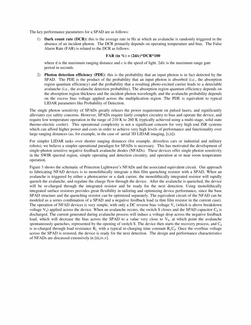
Figure 3 shows the schematic of Princeton Lightwave’s NFADs and the associated equivalent circuit. Our approach
to fabricating NFAD devices is to monolithically integrate a thin film quenching resistor with a SPAD. When an
avalanche is triggered by either a photocarrier or a dark carrier, the monolithically integrated resistor will rapidly
quench the avalanche, and regulate the charge flow through the device. After the avalanche is quenched, the device
will be re-charged through the integrated resistor and be ready for the next detection. Using monolithically
integrated surface resistors provides great flexibility in tailoring and optimizing device performance, since the base
SPAD structure and the quenching resistor can be optimized separately. The equivalent circuit of the NFAD can be
modeled as a series combination of a SPAD and a negative feedback load (a thin film resistor in the current case).
The operation of NFAD devices is very simple, with only a DC reverse bias voltage Va (which is above breakdown
voltage Vb) applied across the device. When an avalanche occurs, the switch S closes and the SPAD capacitor Cd is
discharged. The current generated during avalanche process will induce a voltage drop across the negative feedback
load, which will decrease the bias across the SPAD to a value very close to Vb, at which point the avalanche
spontaneously quenches, represented by the opening of switch S. The device then starts the recovery process, and Cd
is re-charged through load resistance RL with a typical re-charging time constant RLCd. Once the overbias voltage
across the SPAD is restored, the device is ready for the next detection. The design and performance characteristics
of NFADs are discussed extensively in [iii,iv,v].
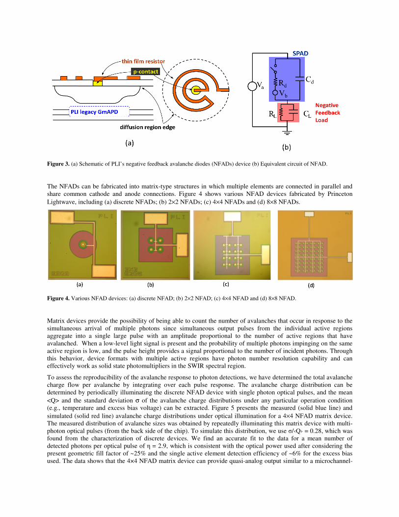
Figure 3. (a) Schematic of PLI’s negative feedback avalanche diodes (NFADs) device (b) Equivalent circuit of NFAD.
The NFADs can be fabricated into matrix-type structures in which multiple elements are connected in parallel and
share common cathode and anode connections. Figure 4 shows various NFAD devices fabricated by Princeton
Lightwave, including (a) discrete NFADs; (b) 2×2 NFADs; (c) 4×4 NFADs and (d) 8×8 NFADs.
Figure 4. Various NFAD devices: (a) discrete NFAD; (b) 2×2 NFAD; (c) 4×4 NFAD and (d) 8×8 NFAD.
Matrix devices provide the possibility of being able to count the number of avalanches that occur in response to the
simultaneous arrival of multiple photons since simultaneous output pulses from the individual active regions
aggregate into a single large pulse with an amplitude proportional to the number of active regions that have
avalanched. When a low-level light signal is present and the probability of multiple photons impinging on the same
active region is low, and the pulse height provides a signal proportional to the number of incident photons. Through
this behavior, device formats with multiple active regions have photon number resolution capability and can
effectively work as solid state photomultipliers in the SWIR spectral region.
To assess the reproducibility of the avalanche response to photon detections, we have determined the total avalanche
charge flow per avalanche by integrating over each pulse response. The avalanche charge distribution can be
determined by periodically illuminating the discrete NFAD device with single photon optical pulses, and the mean
<Q> and the standard deviation σ of the avalanche charge distributions under any particular operation condition
(e.g., temperature and excess bias voltage) can be extracted. Figure 5 presents the measured (solid blue line) and
simulated (solid red line) avalanche charge distributions under optical illumination for a 4×4 NFAD matrix device.
The measured distribution of avalanche sizes was obtained by repeatedly illuminating this matrix device with multi-
photon optical pulses (from the back side of the chip). To simulate this distribution, we use σ/‹Q› = 0.28, which was
found from the characterization of discrete devices. We find an accurate fit to the data for a mean number of
detected photons per optical pulse of η = 2.9, which is consistent with the optical power used after considering the
present geometric fill factor of ~25% and the single active element detection efficiency of ~6% for the excess bias
used. The data shows that the 4×4 NFAD matrix device can provide quasi-analog output similar to a microchannel-
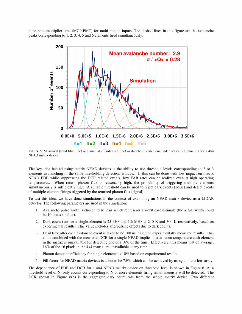
plate photomultiplier tube (MCP-PMT) for multi-photon inputs. The dashed lines in this figure are the avalanche
peaks corresponding to 1, 2, 3, 4, 5 and 6 elements fired simultaneously.
Figure 5. Measured (solid blue line) and simulated (solid red line) avalanche distributions under optical illumination for a 4×4
NFAD matrix device.
The key idea behind using matrix NFAD devices is the ability to use threshold levels corresponding to 2 or 3
elements avalanching in the same thresholding detection window. If this can be done with low impact on matrix
NFAD PDE while suppressing the DCR related events, low FAR rates can be realized even at high operating
temperatures. When return photon flux is reasonably high, the probability of triggering multiple elements
simultaneously is sufficiently high. A suitable threshold can be used to reject dark events (noise) and detect events
of multiple element firings triggered by the returned photon flux (signal).
To test this idea, we have done simulations in the context of examining an NFAD matrix device as a LIDAR
detector. The following parameters are used in the simulation:
1. Avalanche pulse width is chosen to be 2 ns which represents a worst case estimate (the actual width could
be 10 times smaller).
2. Dark count rate for a single element is 25 kHz and 1.6 MHz at 240 K and 300 K respectively, based on
experimental results. This value includes afterpulsing effects due to dark counts.
3. Dead time after each avalanche event is taken to be 100 ns, based on experimentally measured results. This
value combined with the measured DCR for a single NFAD implies that at room temperature each element
in the matrix is unavailable for detecting photons 16% of the time. Effectively, this means that on average,
16% of the 16 pixels in the 4x4 matrix are unavailable at any time.
4. Photon detection efficiency for single elements is 10% based on experimental results.
5. Fill factor for NFAD matrix devices is taken to be 75%, which can be achieved by using a micro-lens array.
The dependence of PDE and DCR for a 4×4 NFAD matrix device on threshold level is shown in Figure 6. At a
threshold level of N, only counts corresponding to N or more elements firing simultaneously will be detected. The
DCR shown in Figure 6(b) is the aggregate dark count rate from the whole matrix device. Two different
0
50
100
150
200
0.0E+0 5.0E+5 1.0E+6 1.5E+6 2.0E+6 2.5E+6 3.0E+6 3.5E+6
Nu
mb
er
of
ev
en
tsMean avalanche number: 2.9
σ / <Q> = 0.28
Simulation
n=1 n=2 n=3 n=4 n=5 n=6

temperatures (240K and 300K) and different photon flux ranging from 10 to 100 photons/pulse have been
considered. The following conclusions can be made from Figure 6:
1. Higher threshold levels reduce the pulse detection probability (PDP) and DCR, with the DCR reducing
more dramatically than PDP. This means that higher SNR can be achieved by increasing the threshold.
2. At higher photon flux levels, increasing threshold has a smaller impact on pulse detection probability.
3. For a given photon flux and threshold level, the pulse detection probability is lower at higher temperatures.
This is because the dead time caused by dark counts results in a loss of single-element detection efficiency.
Higher temperature implies higher dark count rates and increased dead time, with a consequent loss of
detection efficiency.
Essentially, Figure 6 can be used in order to assess the minimum photon flux, maximum operating temperature and
threshold level for a given PDP and DCR. The maximum DCR for the matrix is arrived at by specification on the
maximum required FAR.
Figure 6. Dependence of (a) pulse detection probability and (b) dark count rate on threshold level. When threshold level is set at
N, only counts corresponding to N or more elements fired simultaneously can be detected.
In summary, we have presented in this article a new type of device called negative feedback avalanche diodes
(NFADs), which have single photon sensitivity in the SWIR spectral region. These devices are achieved through
monolithic integration of thin film resistors on top of InP-based single photon avalanche diodes (SPADs). This
design approach minimizes parasitic capacitance and greatly improves device performance. This approach leverages
Princeton Lightwave’s industry-leading performance SPAD design platform, and provides a high degree of
flexibility and control. The operation of the NFAD is very simple, since only a DC bias is required. Further, such
devices can be used at room temperature in conjunction with Princeton Lightwave’s single or multi-mode 1550 nm
lasers for short distance, photon-starved LIDAR applications. For longer distances, these devices can be used with
Princeton Lightwave’s higher power, 1550 nm multi-mode lasers.
About the Author
Dr. Xudong Jiang is a Senior Staff Engineer at Princeton Lightwave Inc. He received B.S., M.S.
and Ph.D. degrees in Physics from Beijing University in 1989, 1992, and 1995, respectively. Dr.
Jiang did postdoctoral work at Harvard University (1995-1996) and Princeton University (1996-
1997) on the electrical and optical properties of superlattices and thin film transistors. Dr. Jiang
joined the University of Florida as co-principal investigator on a project funded by the US Army
Research Office and focused on MWIR and LWIR quantum well infrared photodetector (QWIP)
design, processing and characterization from 1997 to 2000. Dr. Jiang joined Multiplex, Inc. in
2000, where he engaged in the development and manufacturing of 980 nm pump laser and electroabsorption
modulated laser devices and modules. While at Multiplex, he was promoted to distinguished member of technical
staff in April 2002 and manager of laser engineering and operation in November 2003. In 2006, Dr. Jiang joined
1E-8
1E-7
1E-6
1E-5
1E-4
1E-3
1E-2
1E-1
1E+0
1E+1
1E+2
1E+3
1E+4
1E+5
0 1 2 3 4 5
Da
rk c
ou
nt
rate
(k
Hz)
Threshold level
240 K
300 K
1E-3
1E-2
1E-1
1E+0
0 1 2 3 4 5
Pu
lse
de
tect
ion
pro
ba
bil
ity
Threshold level
Ph#/pulse 10 240KPh#/pulse 20 240KPh#/pulse 50 240KPh#/pulse 100 240KPh#/pulse 10 300KPh#/pulse 20 300KPh#/pulse 50 300KPh#/pulse 100 300K
(a) (b)

Princeton Lightwave Inc., where he currently leads programs focused on the design and characterization of high-
performance photodetectors and detector-based products. Dr. Jiang is the author/co-author of more than 40 technical
publications on solid state physics and optoelectronic devices.
i Mark Itzler and Mark Entwistle, “FOCAL-PLANE ARRAYS: Geiger-mode focal plane arrays enable SWIR 3D imaging”,
Laser Focus World 47, March 2011. ii M. Entwistle, M.A. Itzler, J. Chen, M. Owens, K. Patel, X. Jiang K. Slomkowski and S. Rangwala, “Geiger-mode APD camera
system for single-photon 3D LADAR imaging”, Proceedings of the SPIE 8375, 83750D (2012). iii M.A. Itzler, X. Jiang, B. Nyman and K. Slomkowski, “InP-based Negative Feedback Avalanche Diodes”, Proceedings of the
SPIE 7222, 72221K (2009). iv X.Jiang, M.A. Itzler, K. O’Donnell, M. Entwistle and K. Slomkowski, “InGaAs/InP Negative Feedback Avalanche Diodes
(NFADs)”, Proceedings of the SPIE 8033, 80330K (2011). v X.Jiang, M.A. Itzler, K. O’Donnell, M. Entwistle and K. Slomkowski, “InGaAs/InP Negative Feedback Avalanche Diodes
(NFADs) and Solid State Photomultipliers (SSPMs)”, Proceedings of the SPIE 8375, 83750U (2012).