Three-Phase to Single-Phase Matrix Converters: New...
12
ﻧﺸﺮﻳﻪ ﻣﻬﻨﺪﺳﻲ ﺑﺮق و اﻟﻜﺘﺮوﻧﻴﻚ اﻳﺮان- دﻫﻢ ﺳﺎل- ﺷ ﻤﺎره دوم- ﭘﺎﺋﻴﺰ و زﻣﺴﺘﺎن1392 Journal of Iranian Association of Electrical and Electronics Engineers - Vol.10- No.2- Fall & Winter 2013 Three-Phase to Single-Phase Matrix Converters: New Topology Based on New Control Method E. Babaei 1 S. H. Hosseini 2 G. B. Gharehpetian 3 1 Associate Professor, Faculty of Electrical and Computer Engineering, University of Tabriz, Tabriz, Iran [email protected] 2 Professor, Faculty of Electrical and Computer Engineering, University of Tabriz, Tabriz, Iran [email protected] 3 Professor, Electrical Engineering Department, Amirkabir University of Technology, Tehran, Iran [email protected] Abstract: In this paper, a new topology is proposed for three-phase to single-phase matrix converters, where more voltage levels are produced in the output in comparison with the conventional topologies. In addition, a new control method based on minimum error between the generated and the desired output voltages is proposed for three-phase to single-phase matrix converters. In the proposed control method, the output voltage is generated by the mixture of different pieces of the input voltages. In other words, by applying this method, the matrix converter operates like a multilevel converter without requiring to any extra elements. Due to the proposed control method, the desired output voltage can be generated with an acceptable accuracy even with unbalanced and significantly distorted input voltage waveforms. The other advantage of the proposed control method is reduction of number of switching which allows low speed semiconductors application in the structure of bidirectional switches required by matrix converters and also reduction in switching losses. Using this strategy, the dt dv / stresses on load are significantly reduced. As a result, the electromagnetic interference (EMI) is considerably decreased in comparison with the other conventional control methods. Simulation results in PSCAD/EMTDC software and experimental results show that the proposed control method operates correctly and confirm the perfect performance of the proposed topology. Keywords: Matrix converter, Three-phase to single-phase converter, Minimum error, Bidirectional switch. Submission date: 11 May 2009 Conditional acceptance date: 9 Oct. 2010 Acceptance date: 10 Oct. 2011 Corresponding author: Ebrahim Babaei Corresponding author’s address: Faculty of Electrical and Computer Engineering, University of Tabriz, Tabriz, Iran. 37
Transcript of Three-Phase to Single-Phase Matrix Converters: New...

1392پائيز و زمستان - ماره دوم ش - سال دهم - برق و الكترونيك ايران نشريه مهندسي
Journal of Iranian Association of E
lectrical and Electronics E
ngineers - Vol.10- N
o.2- Fall &
Winter 2013
Three-Phase to Single-Phase Matrix Converters: New Topology Based on New Control Method
E. Babaei1 S. H. Hosseini2 G. B. Gharehpetian3
1 Associate Professor, Faculty of Electrical and Computer Engineering, University of Tabriz, Tabriz, Iran [email protected]
2 Professor, Faculty of Electrical and Computer Engineering, University of Tabriz, Tabriz, Iran [email protected]
3 Professor, Electrical Engineering Department, Amirkabir University of Technology, Tehran, Iran [email protected]
Abstract: In this paper, a new topology is proposed for three-phase to single-phase matrix converters, where more voltage levels are produced in the output in comparison with the conventional topologies. In addition, a new control method based on minimum error between the generated and the desired output voltages is proposed for three-phase to single-phase matrix converters. In the proposed control method, the output voltage is generated by the mixture of different pieces of the input voltages. In other words, by applying this method, the matrix converter operates like a multilevel converter without requiring to any extra elements. Due to the proposed control method, the desired output voltage can be generated with an acceptable accuracy even with unbalanced and significantly distorted input voltage waveforms. The other advantage of the proposed control method is reduction of number of switching which allows low speed semiconductors application in the structure of bidirectional switches required by matrix converters and also reduction in switching losses. Using this strategy, the dtdv / stresses on load are significantly reduced. As a result, the electromagnetic interference (EMI) is considerably decreased in comparison with the other conventional control methods. Simulation results in PSCAD/EMTDC software and experimental results show that the proposed control method operates correctly and confirm the perfect performance of the proposed topology.
Keywords: Matrix converter, Three-phase to single-phase converter, Minimum error, Bidirectional switch.
Submission date: 11 May 2009
Conditional acceptance date: 9 Oct. 2010
Acceptance date: 10 Oct. 2011
Corresponding author: Ebrahim Babaei
Corresponding author’s address: Faculty of Electrical and Computer Engineering, University of Tabriz, Tabriz, Iran.
37

Jour
nal o
f Ira
nian
Ass
ocia
tion
of E
lect
rical
and
Ele
ctro
nics
Eng
inee
rs -
Vol
.10-
No.
2- F
all &
Win
ter
2013
1392پائيز و زمستان - ماره دوم ش - سال دهم - برق و الكترونيك ايران نشريه مهندسي 1392پائيز و زمستان - ماره دوم ش - سال دهم - برق و الكترونيك ايران نشريه مهندسي
1. Introduction Matrix converters are direct ac/ac converters which convert input line voltages into variable voltage with unrestricted frequency without using any intermediate dc link circuit [1]. In recent years, the matrix converters have received considerable attention because they may become a good alternative to voltage source inverter pulse width modulation (PWM) topology. This is because of the fact that the matrix converter provides bidirectional power flow and nearly sinusoidal input/output waveforms. Furthermore, the matrix converter allows a compact design due to the elimination of dc link capacitors. On the other hand, the complexity of the matrix converter topology makes the study and the determination of suitable modulation strategies a difficult task [2].
Several solutions based on different mathematical approaches have been presented in the past. Each of them shows different features in terms of the number of switches commutations in a cycle period and full utilization of the input voltages. Alesina and Venturini proposed the principles of matrix converter control in 1981 (AV method) [3]. In the original theory, the output/input voltage transfer ratio was limited to 0.5, but it was shown later that, by means of third harmonic injection techniques (optimum AV method), the maximum output/input voltage transfer ratio could be increased up to 0.866, a value which represents an intrinsic limitation of the three-phase matrix converters with balanced supply voltages [4].
The scalar control modulation algorithm presented in [5], although based on a different approach, leads to performance similar to that obtained using the optimum AV method. A sensible increase of the maximum voltage transfer ratio up to 1.053 is a feature of the fictitious dc link algorithm, presented in [6]. This strategy considers the modulation as a two-step process, namely, rectification and inversion. The higher voltage transfer ratio is achieved in spite of low frequency distortion in the input and output variables [2].
The space-vector modulation approach was initially presented in [7] to control only the output voltages. This method has been successively developed in [2] and [8] in order to exploit the possibility of matrix converters in controlling input power factor regardless of the output power factor, to fully utilize the input voltages and to reduce the number of switch commutations in each cycle period.
The above modulation methods are the basic modulation techniques and the other presented methods mostly try to eliminate weak points of the previous methods [9-12].
The previous methods are generally based on PWM technique and contain some limitations. One of them is low voltage transfer ratio. In addition, if the input voltages are significantly distorted then these methods can not produce the desired output voltage. It is important to note that the matrix converters are direct
converters and any distributions and unbalances in the input sides are immediately reflected to the output side.
The above-mentioned control methods are generally related to three-phase to three-phase matrix converters. In some applications, it is necessary to feed the single-phase loads from the three-phase network with a different frequency and amplitude. For such conversions, three-phase to single-phase converters are necessary. The generally used method in industry for such conversion is dc link based converters. The ac/ac converters with dc links are the most common type of converters for ac/ac conversion. These converters are two-stage converters whose instantaneous operation is decoupled by an energy storage element (a capacitor or an inductoror). In this type of converters, firstly, the ac input voltage is rectified to dc voltage and then its inverted into an ac voltage with changeable frequency and amplitude. They need bulky capacitor banks which results in a slow dynamic response. Due to the consideraby high price and size of the energy storing elements, these coverters are bulky and expensive and difficult to control the stored energy in case of faults.
Cycloconevrters are another common method for three-phase to single-phase conversion. Cycloconverters are direct frequency converters that convert the ac input with a frequency to the ac output with another frequency without using an intermidite stage converter. They are used in high power motor drives and slip energy regeneration. In oredr to have a high effeciency, the output frequency is limited to a third of the input frequency. More complex cycloconvertors to increase the frequency range which use forced commutation and load commutation techniques have been presented. Due to need for a load with specific characteristics, intrinsic complexity and the economical considerations, this type of cycloconverters have not been widely used in industry.
The three-phase to single-phase matrix converters are another possible method for three-phase to single-phase conversion. Matrix converters do not need energy storing elements. According to the authors’ studies, limited number of control procedures for three-phase to single-phase matrix converters have been presented in the literature. These control methods are based on PWM techniques. When the switching frequency is high, due to intrinsic characteristic of these techniques, low order harmonics will be absent on the output side but input and output total harmonic distortion (THD) will be considerably high. In addition, because of the high switching frequency, the efficiency of the converter is low. High /dv dt will result in high EMI and high stress on switches [13-21].
In this paper, a new topology for three-phase to single-phase matrix converters is proposed which considerably reduces the before-mentioned pitfalls. In addition, a new control method based on minimum error between the measured and desired output voltages is proposed. The performance of both topology and the control method is verified by simulation (using PSCAD/EMTDC software) and experimental results.
38

1392پائيز و زمستان - ماره دوم ش - سال دهم - برق و الكترونيك ايران نشريه مهندسي
Journal of Iranian Association of E
lectrical and Electronics E
ngineers - Vol.10- N
o.2- Fall &
Winter 2013
2. Conventional Three-Phase to Single-Phase Matrix Converters A matrix converter consists of n power switches and
can create n2 numbers of on and off states (modes). The following two basic rules should be considered for the correct operation of the converter:
• Short-circuit occurrence among power supplies must be avoided (over current constraint),
• Open circuit in the loads with inductive properties must be avoided (over voltage constraint).
2.1. Three-Phase to Single-Phase Matrix Converter with Three Bidirectional Power Switches The structure of a three-phase to single-phase matrix converter with 3 bidirectional switches is illustrated in Fig. 1. The input voltages of the converter are 1iv , 2iv
and 3iv and the currents through them are 1ii , 2ii and
3ii , respectively. The output voltage and current of the
converter are ov and oi , respectively. The input
voltages of the converter under balanced condition are considered as follows:
)120sin()(
)120sin()(
)sin()(
3
2
1
o
o
+=
−=
=
tVtv
tVtv
tVtv
iimi
iimi
iimi
ωωω
(1)
where imV and iω are the amplitude and angular
frequency of the input voltage, respectively. The fundamental component of the desired output
voltage )( ,Desiredov is considered as follows:
)sin()(, tVtv oomDesiredo ω= (2)
where omV and oω are is the amplitude and angular
frequency of the desired output voltage, respectively. Generally, any arbitrary phase can be considered
for output voltage. The relationship between imV and
omV can be expressed in terms of voltage transfer ratio
)(q as follows:
im
om
V
Vq = (3)
As mentioned, the matrix converters require bidirectional switches for power transmission. Several methods exist to make bidirectional switches [22-23]. In this paper, the common emitter configuration has been used. This configuration consists of two insulated gate bipolar transistors (IGBT) and two reverse parallel diodes as shown in Fig. 1.
The matrix converter with three power switches can produce eight modes while just three modes of them are acceptable considering two mentioned rules in section 2. In Table 1, the permitted modes are presented. As indicated, the maximum instantaneous output voltage amplitude is limited to maximum input voltage amplitude. According to Table 1, three different voltages 21,( ii vv and )3iv can be generated at
the output of this converter.
Fig. 1: Three-phase to single-phase matrix converter with three
switches
Table 1: Permitted modes for a three-phase to single-
phase matrix converter with three switches
Modeoi , Modeov , On Switch Mode
1ii 1iv 1S 1
2ii 2iv 2S 2
3ii 3iv 3S 3
2.2. Three-Phase to Single-Phase Matrix Converter with Six Bidirectional Power Switches The power circuit of three-phase to single-phase matrix converter with six power switches is shown in Fig. 2. This circuit has six power switches that are 11S , 12S ,
21S , 22S , 31S and 32S which totally produce 6426 =
modes but considering two explained rules, the numbers of usable modes are restricted to seven modes that are summarized in Table 2. As shown in this table, at the output of this converter, seven different voltage levels can be produced (considering positive, negative and zero values). In the case of strongly capacitive load connection to the matrix converter, the seventh mode should be ignored. As this table illustrates, the maximum instantaneous output voltage amplitude is
limited to 3 times of the maximum input voltage amplitude. Considering the increased the number of modes, the capability of this circuit overcomes the previous circuit and can produce the output waveform with fewer additive steps in comparison with the previous circuit. As a result, it can produce the output voltage with higher quality.
1iv
2iv
3iv
ov
1S
2S
3S
1ii
2ii
3ii
oi
+
−
39

Jour
nal o
f Ira
nian
Ass
ocia
tion
of E
lect
rical
and
Ele
ctro
nics
Eng
inee
rs -
Vol
.10-
No.
2- F
all &
Win
ter
2013
1392پائيز و زمستان - ماره دوم ش - سال دهم - برق و الكترونيك ايران نشريه مهندسي 1392پائيز و زمستان - ماره دوم ش - سال دهم - برق و الكترونيك ايران نشريه مهندسي
Fig. 2: Three-phase to single-phase matrix converter with six
switches Table 2: Permitted modes for three-phase to single-phase
matrix converter with six switches
Modeoi , Modeov , On Switches Mode
21 ii ii −= 21 ii vv − 2211 & SS 1
31 ii ii −= 31 ii vv − 3211 & SS 2
12 ii ii −= 12 ii vv − 2112 & SS 3
32 ii ii −= 32 ii vv − 2132 & SS 4
13 ii ii −= 13 ii vv − 3112 & SS 5
23 ii ii −= 23 ii vv − 2231 & SS 6
oi 0
)&( 1211 SS or
)&( 2221 SS or
)&( 3231 SS
7
3. Proposed Topology for Three-Phase to Single-Phase Matrix Converter In order to increase the number of modes of three-phase to single-phase matrix converters in comparison with the previously discussed two converters, a three-phase to single-phase matrix converter with eight bidirectional power switches is proposed as shown in Fig. 3. This converter has two more switches of PS
and NS in comparison with the matrix converters with
six switches. The converter with eight switches
generates 25628 = modes but taking the two mentioned rules into account, thirteen permitted modes can be created according to Table 3. In the case of strongly capacitive load connection to the matrix converter, the thirteenth mode should be ignored. As this table illustrates, the maximum instantaneous output
voltage amplitude is limited to 3 times of the maximum input voltage amplitude. Considering the increased number of modes, the capability of this circuit overcomes the previous topologies and can produce the output voltage with less additive steps than
previous circuits. As a result, it can produce the output voltage waveform with higher quality.
Fig. 3: Proposed topology for three-phase to single-phase
matrix converter
Table 3: Permitted modes for the proposed topology
Modeoi , Modeov , On Switches Mode
21 ii ii −= 21 ii vv − 2211 & SS 1
31 ii ii −= 31 ii vv − 3211 & SS 2
12 ii ii −= 12 ii vv − 2112 & SS 3
32 ii ii −= 32 ii vv − 2132 & SS 4
13 ii ii −= 13 ii vv − 3112 & SS 5
23 ii ii −= 23 ii vv − 2231 & SS 6
1ii 1iv 11& SSP 7
2ii 2iv 21& SSP 8
3ii 3iv 31& SSP 9
1ii− 1iv− 12& SSN 10
2ii− 2iv− 22& SSN 11
3ii− 3iv− 32& SSN 12
oi 0
)&( 1211 SS or
)&( 2221 SS or
)&( 3231 SS or
)&( NP SS
13
4. Relation between Output Voltage and Current The relationship between the output voltage and current in three-phase to single-phase converters for
LR − load can be expressed as follows:
dt
tdiLtRitv o
oo)(
)()( += (4)
1iv
2iv
3iv
11S1ii
2ii
3ii
ov
oi
+ −
12S
21S 22S
31S 32S
1iv
3iv
11S1ii
2ii
3ii
ov
oi
+ −
12S
21S 22S
31S 32S
NS
PS
2iv
40
1392پائيز و زمستان - ماره دوم ش - سال دهم - برق و الكترونيك ايران نشريه مهندسي
Journal of Iranian Association of E
lectrical and Electronics E
ngineers - Vol.10- N
o.2- Fall &
Winter 2013
Considering (2), the fundamental component of the output current can be calculated as:
−+
= −
R
Lt
RL
Vti o
o
o
omo
ωωω
1
22tansin
)()( (5)
5. Proposed Control Method The majority of the presented control methods for controlling the matrix converters need balanced input voltages and if an unbalance whether in amplitude or in phase angle occurs in the input voltages, these control methods usually fail to operate properly. In addition, the conventional control methods are generally based on PWM techniques. In these techniques, the switching frequency is chosen so high that does not affect the load. There are several methods to generate PWM pulses. With these techniques, the THD of the output voltages increases but in return the resulting harmonics are generated around the switching frequency. Although the PWM technique has particular advantages, but it has some disadvantages as follows: • The control techniques based on PWM, need
high switching frequencies up to several kHz to maintain their advantages. This factor causes an increase in commutation frequency. It should be mentioned that the commutation problem is one of the factors that prevents matrix converters from finding their specific place in industry.
• Due to high switching frequency of PWM based techniques, the application of semiconductor based instruments with high connection and disconnection frequency are required. It is clear that high power and the high connect/disconnect frequency semiconductor instruments are too expensive. As a result, the total cost of converter is increased.
• Because of applying high frequency switching method, the PWM techniques have high switching losses which cause decline in efficiency of the converter.
• Due to intrinsic pitfalls of these techniques, the output voltage usually would be like a train of square pulses. Because of great difference between low level voltage and high level voltage, these techniques generate high dtdv / stress on the load. As a result, the EMI effect is increased.
• The application of PWM techniques generates harmonics too far from the fundamental frequency around the switching frequency. Therefore the size of passive components is reduced to remove harmonics. However, these techniques generally have a very high THD.
• Generally, applying PWM techniques, the voltage transfer ratio of matrix converters become lower than unity that is considered as
one of the main disadvantages of these methods and limits their application.
In this paper, a new control method is proposed for three-phase to single-phase matrix converters which is based on different technique from PWM techniques. In the world of intelligent systems, there are several methods to explain a scientific subject. Maybe one of these methods is applying natural language that is usually called IF-THEN rule:
IF promise THEN conclusion
In the proposed control method, the generated output voltage is compared with the desired output voltage in various operation modes of converter. In other words, in different operation modes of matrix converter, the error between the desired and generated output voltages is explained as follows:
L,2,1)()()( ,,, =−= jtvtvtE jModeoDesiredoj (6)
In this equation, jE is the error of voltage and
jModeov ,, is the generated output voltage during j th
mode. This control method is based on the minimum error between the desired and generated output voltages. In other words:
ONbewillkModeinswitchesTheTHEN
EEEEIF
ONbewillModeinswitchesTheTHEN
EEEEIF
ONbewillModeinswitchesTheTHEN
EEEEIF
Kk
k
k
)),,,(min(
2
)),,,(min(
1
)),,,(min(
21
221
121
==
==
==
L
M
L
L
(7)
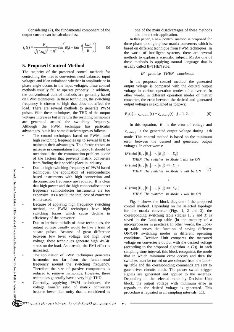
Fig. 4 shows the block diagram of the proposed control method. Depending on the selected topology for the matrix converter (Figs. 1, 2 and 3), the corresponding switching table (tables 1, 2 and 3) is saved in the Look-up table (in the memory of a microprocessor in practice). In other words, the Look-up table serves the function of saving different ON/OFF switching modes in different operating conditions. Decision Unit compares the measured voltage on converter’s output with the desired voltage (according to the proposed algorithm in (7)). In each sampling time interval, this block recognizes the mode that in which minimum error occurs and then the switches must be turned on are selected from the Look-up table and the corresponding commands are sent to gate driver circuits block. The power switch trigger signals are generated and applied to the switches. Depending on the selected mode by Decision Unit block, the output voltage with minimum error in regards to the desired voltage is generated. This procedure is repeated in all sampling intervals [11].
41
Jour
nal o
f Ira
nian
Ass
ocia
tion
of E
lect
rical
and
Ele
ctro
nics
Eng
inee
rs -
Vol
.10-
No.
2- F
all &
Win
ter
2013
1392پائيز و زمستان - ماره دوم ش - سال دهم - برق و الكترونيك ايران نشريه مهندسي 1392پائيز و زمستان - ماره دوم ش - سال دهم - برق و الكترونيك ايران نشريه مهندسي
Fig. 4: Block diagram of the proposed control method
In the proposed control method, the matrix converters operate as a multilevel converter. As the simulation and experimental results will show, one of the most important advantages of this control method is that even for unbalanced and significantly distorted input voltages, the desired output voltage can be acceptably produced with minimum error.
The main disadvantage of this method is that, for little changes in voltage transfer ratio, there might not be noticeable changes in the waveform of the output voltage of the converter. In addition, it does not guarantee that the amplitude of fundamental component of the measured output voltage exactly equals to the desired output voltage. Therefore, with this control method, there is an error in the amplitude of fundamental component. To investigate this subject, a concept named as percentage of voltage error is considered for matrix converters, which presents the percentage of error between generated voltage and the expected output voltage. The percentage of voltage error for matrix converters is defined as follows [11]:
100% , ×−
=om
Funomom
V
VVError (8)
where FunomV , is the amplitude of fundamental
component of the generated output voltage. The positive voltage error shows that the amplitude
of the generated output voltage should be increased in order to achieve the desired output voltage. Also, the negative voltage error shows that the amplitude of the output voltage should be decreased to achieve the expected output voltage.
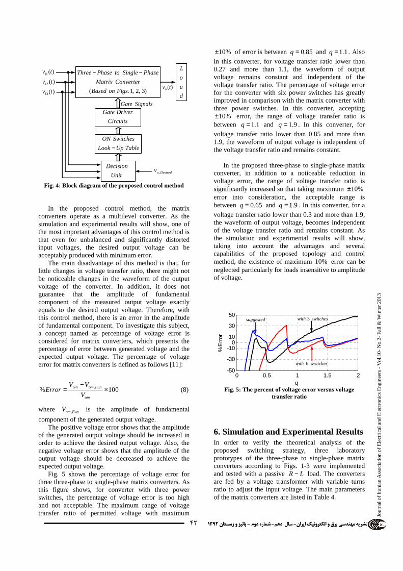
Fig. 5 shows the percentage of voltage error for three three-phase to single-phase matrix converters. As this figure shows, for converter with three power switches, the percentage of voltage error is too high and not acceptable. The maximum range of voltage transfer ratio of permitted voltage with maximum
%10± of error is between 85.0=q and 1.1=q . Also
in this converter, for voltage transfer ratio lower than 0.27 and more than 1.1, the waveform of output voltage remains constant and independent of the voltage transfer ratio. The percentage of voltage error for the converter with six power switches has greatly improved in comparison with the matrix converter with three power switches. In this converter, accepting
%10± error, the range of voltage transfer ratio is between 1.1=q and 9.1=q . In this converter, for
voltage transfer ratio lower than 0.85 and more than 1.9, the waveform of output voltage is independent of the voltage transfer ratio and remains constant.
In the proposed three-phase to single-phase matrix
converter, in addition to a noticeable reduction in voltage error, the range of voltage transfer ratio is significantly increased so that taking maximum %10± error into consideration, the acceptable range is between 65.0=q and 9.1=q . In this converter, for a
voltage transfer ratio lower than 0.3 and more than 1.9, the waveform of output voltage, becomes independent of the voltage transfer ratio and remains constant. As the simulation and experimental results will show, taking into account the advantages and several capabilities of the proposed topology and control method, the existence of maximum %10 error can be neglected particularly for loads insensitive to amplitude of voltage.
Fig. 5: The percent of voltage error versus voltage
transfer ratio
6. Simulation and Experimental Results In order to verify the theoretical analysis of the proposed switching strategy, three laboratory prototypes of the three-phase to single-phase matrix converters according to Figs. 1-3 were implemented and tested with a passive LR − load. The converters are fed by a voltage transformer with variable turns ratio to adjust the input voltage. The main parameters of the matrix converters are listed in Table 4.
0 0.5 1 1.5 2-50
-30
-100
10
30
50
q
%E
rror
switcheswith 3
switcheswith 6
suggested
)(tvo
)(1 tvi
Desiredov ,
SignalsGate
)3,2,1.( FigsonBased
ConverterMatrix
PhaseSingletoPhaseThree −−
TableUpLook
SwitchesON
−
Unit
Decision
d
a
o
L
Circuits
DriverGate
)(2 tvi
)(3 tvi
42

1392پائيز و زمستان - ماره دوم ش - سال دهم - برق و الكترونيك ايران نشريه مهندسي
Journal of Iranian Association of E
lectrical and Electronics E
ngineers - Vol.10- N
o.2- Fall &
Winter 2013
Table 4. Main parameters of the matrix converters Parameter Value
imV 120V
omV 140V
if 50Hz
of 100Hz
L 55mH R 40Ω
sf 1000Hz
Each bidirectional switch can be driven with respect to the common point, i.e. the common emitter can be considered as a local ground for a bidirectional switch. On the other hand, in order to ensure a correct operation, each bidirectional switch requires an isolated power supply.
Fig. 6 shows the isolator and driver circuit of each bidirectional switch. This circuit consists of an opto-isolator, a schmit trigger and a buffer. As mentioned, each bidirectional switch in the matrix converters requires an isolated driver circuit. The isolation can be provided using either pulse transformers or opto-isolators. Opto-isolators can operate in a wide range of input signal pulse width but a separate isolated power supply is required for each switching device. The opto-isolator based on the gate driver circuit is used in the prototypes.
The square safe operating area of the IGBT for switch mode operation minimizes the need for snubber circuits in most applications such as the voltage source inverter. However, it is necessary to use a snubber circuit in the matrix converters due to the absence of freewheeling paths. In the matrix converters, the load current is always commutated from one controlled switch to another. In these converters, a time delay can be easily introduced between drive signals for complementary devices in order to avoid simultaneous conduction. During this delay time, the inductive load current is taken over by a snubber circuit [11]. In these converters, a small CR − turn-off snubber circuit as depicted in Fig. 6 is connected across each bidirectional switch to limit the device voltage to an appropriate level. It is important to mention that the main focus of this paper is to develop the switching strategies and therefore the problem of optimized snubber circuit design is not pursued further. The values of R and C in the snubber circuit are Ω10 and
Fµ022.0 , respectively. The 89C52 microcontroller by
ATMEL Company has been used to generate the switching patterns according to the proposed switching strategies. The IGBTs are the type BUP306D with internal anti-parallel diodes.
To examine the performance of the proposed converter and control method in the generation of a desired output voltage waveform, the matrix converters shown in Figs. 1-3 are simulated by PSCAD software.
In addition, to confirm the simulation results, three prototypes are implemented based on the topologies shown in Figs. 1-3. The simulation and experimental results for each topology of three-phase to single-phase matrix converters will be presented in the next parts.
Fig. 6: Gate driver circuit of bidirectional switch
6.1. Simulation and Experimental Results for Balanced Inputs
In the first experiment, the input and output voltages are considered as (1) and (2), respectively. Fig. 7 shows the simulation and experimental results for output voltage. As shown in this figure, the output voltage consists of some pieces of input voltages. The waveform of the output voltage in the proposed converter is very close to the expected output waveform. In addition, dtdv / variations in the output voltage are lower and decreasing the EMI. It should be noticed that dtdv / variations in the proposed topology are fewer than the conventional topologies. It is necessary to mention that the experimental results are exactly similar to the simulation results. Fig. 8 shows the simulation and experimental results for the output current. As this figure shows, the current waveform in the proposed converter is very similar to sinusoidal waveform because the output voltage is similar to sinusoidal waveform.
Fig. 9 shows the spectrums of voltages and currents for the three converters. Since the load of the converters )( LR − is almost a low pass filter, the
output current contains less high-order harmonics than the output voltage. This figure shows that the amplitude of the fundamental component of the output voltage in the proposed converter has less error than the conventional converters. In addition, in the proposed topology the generated harmonics are much fewer than other topologies. The percentage of error for three-phase to single-phase converters with three, six and eight power switches are equal to %15.4, %7− and %3.5, respectively, and exactly complies with the results of Fig. 5.
As the waveforms of the output voltages show, the
converters can generate the desired output voltages with minimum number of switching. The maximum
isolator
Opto −Trigger
SchmitBuffer
DriverGate
Signal
InputR
C
43

Jour
nal o
f Ira
nian
Ass
ocia
tion
of E
lect
rical
and
Ele
ctro
nics
Eng
inee
rs -
Vol
.10-
No.
2- F
all &
Win
ter
2013
1392پائيز و زمستان - ماره دوم ش - سال دهم - برق و الكترونيك ايران نشريه مهندسي 1392پائيز و زمستان - ماره دوم ش - سال دهم - برق و الكترونيك ايران نشريه مهندسي
number of switching among the converters belongs to the proposed converter (the topology shown in Fig. 3). However, even in the proposed converter, applying the proposed control method, the number of switching is considerably reduce in comparison with that of the PWM based methods. In order to indicate this, the on/off commands of the switches of the proposed converter are shown in Fig. 11. As this figure shows, the desired output voltage is generated with lower number of switching that leads to reduction in switching losses. In addition, it is possible to apply low speed semiconductor in the structure of matrix converters. As a result, the cost of converter is significantly reduced.
Table 5 shows the THDs of the output voltage and
output current based on simulations for three converters with amplitude of up to the 63th harmonic. Reduction of THD is achieved by the proposed topology. As this table shows, the THD in the proposed method is much less than PWM method. Moreover the amount of THD in the proposed topology is lower than other topologies that shows the good quality of the proposed converter.
3-Phase to Single-Phase with 3-Switch (BIBO)
0.0000 0.0100 0.0200 0.0300 0.0400
-200 -150 -100 -50
0 50
100 150 200
Vo,Desired Vo,Measured
(a) With three power switches
3-Phase to Single-Phase with 6-Switch (BIBO)
0.0000 0.0100 0.0200 0.0300 0.0400
-200 -150 -100 -50
0 50
100 150 200
Vo_Desired Vo_Measured
(b) With six power switches
3-Phase to Single-Phase with 8-Switch (BIBO)
0.0000 0.0100 0.0200 0.0300 0.0400
-200 -150 -100 -50
0 50
100 150 200
Vo,Desired Vo,Measured
(c) Proposed topology
Fig. 7: Output voltage under balanced operation (Left column: Simulation; Right column: Experimental)
3-Phase to Single-Phase with 3-Switch (BIBO)
0.0000 0.0100 0.0200 0.0300 0.0400
-3.0 -2.0 -1.0 0.0 1.0 2.0 3.0
Io
(a) With three power switches
3-Phase to Single-Phase with 6-Switch (BIBO)
0.0000 0.0100 0.0200 0.0300 0.0400
-4.0 -3.0 -2.0 -1.0 0.0 1.0 2.0 3.0 4.0
Io
3-Phase to Single-Phase with 8-Switch (BIBO)
0.0000 0.0100 0.0200 0.0300 0.0400
-3.0 -2.0 -1.0 0.0 1.0 2.0 3.0
Io
(b) With six switches c) proposed topology
Fig. 8: Output current under balanced operation
(a) With three power switches
(b) With six power switches
(c) Proposed topology
Fig. 9: FFTs of output voltage and current under balanced operation (Left column: Output voltage; Right
column: Output current)
Table 5: THDs of output voltage and current
With three switches
With six switches
Proposed topology
THD of output voltage
%40.7 %33.44 %12.1
THD of output current
%20.02 %12.03 %2.903
44

1392پائيز و زمستان - ماره دوم ش - سال دهم - برق و الكترونيك ايران نشريه مهندسي
Journal of Iranian Association of E
lectrical and Electronics E
ngineers - Vol.10- N
o.2- Fall &
Winter 2013
Fig. 10: Commands of switches for the proposed topology
6.2. Simulation and Experimental Results for Unsinusoidal Output
In the proposed control method, the expected distorted output voltage can be generated from balanced inputs. To show this capability, the desired output voltage is considered as follows:
)5cos(2.03sin4.0sin1.1)( tVtVtVtv iomiomiomo ωωω ++= (9)
Fig. 11 shows the simulation and experimental results of output voltage for each three converters. As these results show, the proposed control method is able to generate the desired output voltage regardless of the
kind of the figure of wave shape. The quality of output waveform in the proposed converter is better than the conventional converters.
3-Phase to Single-Phase with 3-Switch (BIUO)
0.0000 0.0100 0.0200 0.0300 0.0400
-200 -150 -100 -50
0 50
100 150 200
Vo,Desired Vo,Measured
(a) With three power switches
3-Phase to Single-Phase with 6-Switch (BIUO)
0.0000 0.0100 0.0200 0.0300 0.0400
-200 -150 -100 -50
0 50
100 150 200
Vo,Desired Vo,Measured
(b) With six power switches
3-Phase to Single-Phase with 8-Switch (BIUO)
0.0000 0.0100 0.0200 0.0300 0.0400
-200 -150 -100 -50
0 50
100 150 200
Vo,Desired Vo,Measured
(c) Proposed topology
Fig. 11: Output voltage under distorted operation (Left column: Simulation; Right column: Experimental)
6.3. Simulation Results for Unbalanced and Distorted Inputs
In order to show more capabilities of the proposed control method, assume that the input voltages are unbalanced and significantly distorted as follows:
)5cos(2.0)270sin(8.0)(
)3cos(3.0)270sin(15.1)(
)2cos(25.0)45sin(2.1)(
tVtVtv
tVtVtv
tVtVtv
iimiimC
iimiimB
iimiimA
ωωωω
ωω
+−=
++=
+−=
o
o
o
(10)
The waveform of output voltage is considered as
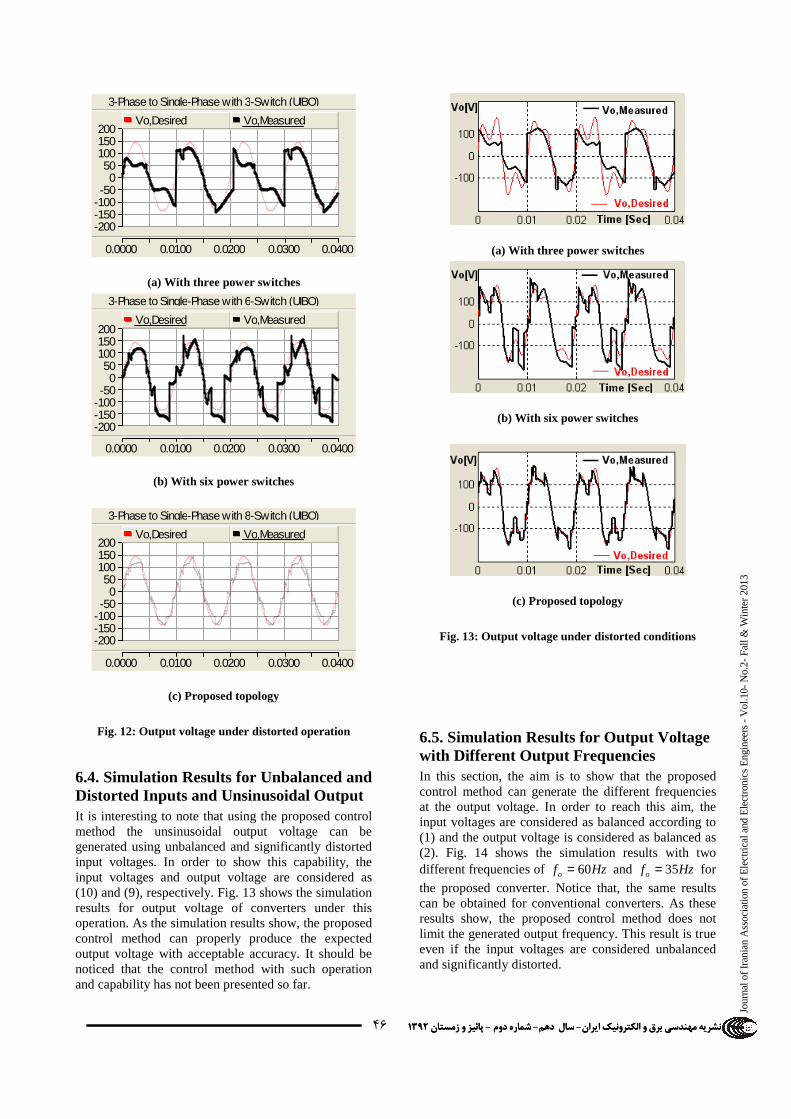
(2). Fig. 12 shows the simulation results for the output voltage of converter under the unbalanced and distorted condition. It is very interesting to note that the proposed control method is one of the particular control methods that can generate the desired output voltage with minimum error from unbalanced and significantly distorted input voltages. As Fig. 12 shows, the quality of the output waveform in the proposed converter is better than the conventional converters.
0.0000 0.0050 0.0100
0.0
1.0
S11
0.0
1.0
S12
0.0
1.0
S21
0.0
1.0
S22
0.0
1.0
S31
0.0
1.0
S32
0.0
1.0
SN
0.0
1.0
SP
[sec]Time
45
Jour
nal o
f Ira
nian
Ass
ocia
tion
of E
lect
rical
and
Ele
ctro
nics
Eng
inee
rs -
Vol
.10-
No.
2- F
all &
Win
ter
2013
1392پائيز و زمستان - ماره دوم ش - سال دهم - برق و الكترونيك ايران نشريه مهندسي 1392پائيز و زمستان - ماره دوم ش - سال دهم - برق و الكترونيك ايران نشريه مهندسي
3-Phase to Single-Phase with 3-Switch (UIBO)
0.0000 0.0100 0.0200 0.0300 0.0400
-200 -150 -100 -50
0 50
100 150 200
Vo,Desired Vo,Measured
(a) With three power switches
3-Phase to Single-Phase with 6-Switch (UIBO)
0.0000 0.0100 0.0200 0.0300 0.0400
-200 -150 -100 -50
0 50
100 150 200
Vo,Desired Vo,Measured
(b) With six power switches
3-Phase to Single-Phase with 8-Switch (UIBO)
0.0000 0.0100 0.0200 0.0300 0.0400
-200 -150 -100 -50
0 50
100 150 200
Vo,Desired Vo,Measured
(c) Proposed topology
Fig. 12: Output voltage under distorted operation
6.4. Simulation Results for Unbalanced and Distorted Inputs and Unsinusoidal Output It is interesting to note that using the proposed control method the unsinusoidal output voltage can be generated using unbalanced and significantly distorted input voltages. In order to show this capability, the input voltages and output voltage are considered as (10) and (9), respectively. Fig. 13 shows the simulation results for output voltage of converters under this operation. As the simulation results show, the proposed control method can properly produce the expected output voltage with acceptable accuracy. It should be noticed that the control method with such operation and capability has not been presented so far.
(a) With three power switches
(b) With six power switches
(c) Proposed topology
Fig. 13: Output voltage under distorted conditions
6.5. Simulation Results for Output Voltage with Different Output Frequencies In this section, the aim is to show that the proposed control method can generate the different frequencies at the output voltage. In order to reach this aim, the input voltages are considered as balanced according to (1) and the output voltage is considered as balanced as (2). Fig. 14 shows the simulation results with two different frequencies of Hzfo 60= and Hzfo 35= for
the proposed converter. Notice that, the same results can be obtained for conventional converters. As these results show, the proposed control method does not limit the generated output frequency. This result is true even if the input voltages are considered unbalanced and significantly distorted.
46
1392پائيز و زمستان - ماره دوم ش - سال دهم - برق و الكترونيك ايران نشريه مهندسي
Journal of Iranian Association of E
lectrical and Electronics E
ngineers - Vol.10- N
o.2- Fall &
Winter 2013
0.000 0.010 0.020 0.030 0.040 0.050 0.060
-200 -150 -100 -50
0 50
100 150 200
Vo,Desired Vo,Measured
(a) Hzfo 35=
0.000 0.010 0.020 0.030 0.040 0.050 0.060
-200 -150 -100 -50
0 50
100 150 200
Vo,Desired Vo,Measured
(b) Hzfo 60=
Fig. 14: Output voltage of proposed topology for different output frequencies
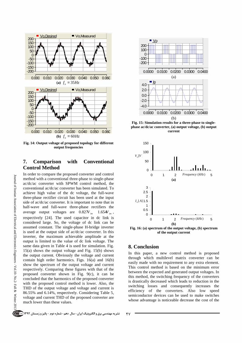
7. Comparison with Conventional Control Method In order to compare the proposed converter and control method with a conventional three-phase to single-phase ac/dc/ac converter with SPWM control method, the conventional ac/dc/ac converter has been simulated. To achieve high value of the dc voltage, the full-wave three-phase rectifier circuit has been used at the input side of ac/dc/ac converter. It is important to note that in half-wave and full-wave three-phase rectifiers the average output voltages are 0.827 imV 1.654 imV ,
respectively [24]. The used capacitor in dc link is considered large. So, the voltage of dc link can be assumed constant. The single-phase H-bridge inverter is used at the output side of ac/dc/ac converter. In this inverter, the maximum achievable amplitude at the output is limited to the value of dc link voltage. The same data given in Table 4 is used for simulation. Fig. 15(a) shows the output voltage and Fig. 15(b) shows the output current. Obviously the voltage and current contain high order harmonics. Figs. 16(a) and 16(b) show the spectrum of the output voltage and current respectively. Comparing these figures with that of the proposed converter shown in Fig. 9(c), it can be concluded that the harmonics of the proposed converter with the proposed control method is lower. Also, the THD of the output voltage and voltage and current is 86.55% and 6.14%, respectively. Considering Table 5, voltage and current THD of the proposed converter are much lower than these values.
0.0000 0.0100 0.0200 0.0300 0.0400
-200 -100
0 100 200
Vo
(a)
0.0000 0.0100 0.0200 0.0300 0.0400
-4.0 -2.0 0.0 2.0 4.0
Io
(b)
Fig. 15: Simulation results for a three-phase to single-phase ac/dc/ac converter, (a) output voltage, (b) output
current
(a)
(b)
Fig. 16: (a) spectrum of the output voltage, (b) spectrum of the output current
8. Conclusion In this paper, a new control method is proposed through which multilevel matrix converter can be easily made with no requirement to any extra element. This control method is based on the minimum error between the expected and generated output voltages. In this method, the switching frequency of the converters is drastically decreased which leads to reduction in the switching losses and consequently increases the efficiency of the converters. Also low speed semiconductor devices can be used to make switches whose advantage is noticeable decrease the cost of the
][ AI o
00.5
11.5
22.5
3
0 1 2 3 4 5)(kHzFrequency
][VVo
0
50
100
150
0 1 2 3 4 5)(kHzFrequency
47
Jour
nal o
f Ira
nian
Ass
ocia
tion
of E
lect
rical
and
Ele
ctro
nics
Eng
inee
rs -
Vol
.10-
No.
2- F
all &
Win
ter
2013
1392پائيز و زمستان - ماره دوم ش - سال دهم - برق و الكترونيك ايران نشريه مهندسي 1392پائيز و زمستان - ماره دوم ش - سال دهم - برق و الكترونيك ايران نشريه مهندسي
converters. In addition, for higher capability of multilevel matrix converters, a new topology by adding two switches to the converter is proposed which permits increasing the modes of matrix converters drastically. The proposed control method and topology has the ability to generate the desired output voltage from any kind of three-phase system regardless of the degree of unbalance and amount of distortion. It should be reminded that although a little error exists in produced amplitude of voltage, in a lot of applications where the consumer is not sensitive to amplitude of voltage, this error does not make any problem. In return, the proposed method has particular capabilities and advantages that are very valuable in the engineering world. In the proposed method, because of remarkable decrease of dtdv / in output voltage, their stresses on the load is extremely decreased. As a result, EMI decreases considerably.
References [1] S. Sunter, “Slip energy recovery of a rotor-side field
oriented controlled wound rotor induction motor fed by matrix converter,” Elsevier Journal of the Franklin Institute, vol. 345, no. 4, pp. 419-435, July 2008.
[2] D. Casadei, G. Serra, A. Tani, and L. Zarri, “Matrix converter modulation strategies: A new general approach based on space-vector representation of the switch state,” IEEE Trans. Ind. Electron., vol. 49, no. 2, pp. 370-381, April 2002.
[3] A. Alesina and M. Venturini, “Solid-state power conversion: A Fourier analysis approach to generalized transformer synthesis,” IEEE Trans. Circuits Syst., vol. CAS-28, pp. 319-330, April 1981.
[4] M.J. Maytum and D. Colman, “The implementation and future potential of the Venturini converter,” in Proc. Drives, Motors Controls, 1983, pp. 108-117.
[5] G. Roy and G.E. April, “Cycloconverter operation under a new scalar control algorithm,” in Proc. PESC, Milwaukee, WI, 1989, pp. 368-375.
[6] P.D. Ziogas, S.I. Khan, and M.H. Rashid, “Analysis and design of forced commutated cycloconverter structures with improved transfer characteristics,” IEEE Trans. Ind. Electron., vol. 1E-33, pp. 271-280, August 1986.
[7] L. Huber and D. Borojevic, “Space vector modulator for forced commutated cycloconverters,” in Proc. Conf. Rec. IEEE-IAS Annu. Meeting, vol. 1, 1989, pp. 871-876.
[8] D. Casadei, G. Serra, and A. Tani, “Reduction of the input current harmonic content in matrix converters under input/output unbalance,” IEEE Trans. Ind. Electron., vol. 45, pp. 401-411, June 1998.
[9] R.T. Sheiner, V.K. Krivovyaz, and A.I. Kalygin, “Coordinate PWM control strategy of the two-stage direct frequency converter,” IEEE 2003, pp. 67-73.
[10] M. Imayavaramban, K. Latha, and G. Uma, “Analysis of different schemes of matrix converter with maximum voltage conversion ratio,” in Proc. MELECON, 2004, Croatia, vol. 3, pp. 1137-1140.
[11] E. Babaei, “Modeling and design of novel control methods of matrix converters,” Ph.D. Thesis, Faculty of Electrical and Computer Engineering, University of Tabriz, Iran, April 2007.
[12] S. Kawak, “Indirect matrix converter drives for unity displacement factor and minimum switching losses,” Elsevier Journal of Electric Power Systems Research, vol. 77, no. 5-6, pp. 447-454, April 2007.
[13] S. Sunter, “A vector controlled matrix converter induction motor drive,” Ph.D. Thesis, University of Nottingham, July 1995.
[14] E. Babaei and A. Aghabeigi, “A new control method for three-phase to single-phase matrix converters,” in Proc. PSC, 2008, Tehran, Iran (in Persian).
[15] E. Babaei and A. Aghabeigi Heris, “PWM-based control strategy for forced commutated cycloconverters,” in Proc. ISIEA, 2009, Kuala Lumpur, Malaysia, vol. 2, pp. 669-674.
[16] E. Babaei, “Control of direct three-phase to single-phase converters under balanced and unbalanced operations,” Elsevier Journal of Energy Conversion and Management, vol. 52, no. 1, pp. 66-74, Jan. 2011.
[17] S.I. Khan, M.H. Rashid, P.D. Ziogas, “Analysis and design of improved three to single phase cycloconverter,” in Proc. IECON, 1988, vol. 3, pp. 603-610.
[18] T.F. Podlesak, J.E.B. Tuttle, P. W. Wheeler; and L. Empringham, “Matrix converter using MOS turn-off thyristors,” in Proc. Twenty-Fourth International Power Modulator Symposium, 2000, pp. 107-110.
[19] E. Babaei, A. Aghagolzadeh, S.H. Hosseini, and S. Khanmohammadi, “A new structure for three-phase to single-phase ac/ac matrix converters,” in Proc. ICECS, 2003, Sharjah, United Arab Emirates (U.A.E.), vol. I, pp. 36-39.
[20] S. Khanmohammadi, A. Aghagolzadeh, S.H. Hosseini, and E. Babaei, “A new algorithm for three-phase to single-phase ac/ac matrix converters,” in Proc. ICECS, 2003, Sharjah, United Arab Emirates (U.A.E.) , vol. III, pp. 1121-1124.
كنترل مستقيم گشتاور و "غالمرضا عرب ماركده، محمد صدوق [21]
خروجي خبا -ايي با خطي سازي وروديضريب توان يك موتور الق
سال هشتم، شماره اول، بهار و تابستان " استفاده از مبدل ماتريسي
1390
[22] E. Babaei, S. H. Hosseini, G. B. Gharehpetian, M. Tarafdar Haque, and M. Sabahi, “Reduction of dc voltage sources and switches in asymmetrical multilevel converters using a novel topology,” Elsevier Journal of Electric Power Systems Research, vol. 77, no. 8, pp. 1073-1085, Jun. 2007.
[23] C. Klumpner and F. Blaabjerg, “Using reverse blocking IGBTs in power converters for adjustable speed drives,” IEEE Trans. Ind. Appl., vol. 42, no. 3, pp. 807-816, May/Jun. 2006.
[24] M.H. Rashid, “Power Electronics Handbook,” Academic Press, 2001.
48