Three-Phase Three-Level Nine Switches Inverter...
7
Abstract— This paper studies the space vector pulse width modulation technique (SVPWM) for the three-phase three- level nine switches voltage source inverter. The proposed inverter is based on the two level inverter topology where it consists of a main inverter switches Q 1 , Q 2 , Q 3 , Q 4 , Q 5 , and Q 6 , an auxiliary three bidirectional switches S 1 , S 2 , and S 3 and two capacitor banks C 1 , and C 2 . Ideal switches and diodes will be assumed and the dc bus capacitor bank voltages fluctuations will be absent. The effectiveness of the SVPWM control scheme will be verified by the simulations results in the worst case where two very low switching frequencies values of 1 kHz and 5 kHz will be considered. Open loop controller experimental measurements at 1 kHz switching frequency will be provided. Index Terms— two level inverter, three-phase three- level inverter, space vector pulse width modulation I. INTRODUCTION Figure 1 shows a three-phase three-level inverter topology based on the two-level inverter topology which has been proposed in [1]. Switches Q 1 , Q 2 , Q 3 , Q 4 , Q 5 , and Q 6 represent the two-level inverter topology besides bidirectional switches S 1, S 2 , and S 3 represent an auxiliary circuit. It employs a simple control scheme at low switching frequency due to that the selected harmonic elimination technique (SHE) has been chosen to generate switches pulses required for optimum operation or lowest voltage output total harmonic distortion (THD). It has been found that switches Q 1 , Q 2 , Q 3 , Q 4 , Q 5 , and Q 6 operate at main line power frequency, while bidirectional switches S 1, S 2 , and S 3 operate at twice main line power frequency. The main line power frequency is chosen at 50 Hz. Such a way of creating output waveforms has some advantages: simple control circuitry besides operation at low switching frequency make the problem of both electromagnetic interference (EMI) and devices voltage stress to be nearly absent. The main disadvantage of such a control method is a high harmonic content of the output voltage-THD amounts to 15.5% which needs extra filter which increases the complexity of the layout circuit and the component used. With the introduction of multi-level voltage-source converters [2], various modulation techniques have been developed for pulse width modulation (PWM). PWM has been studied extensively during the past decades. Many different PWM methods have been developed to achieve less THD, easy implementation and less computation time. With the development of microprocessors, space- vector modulation (SVM) has become one of the most important PWM methods for three-phase converters [3]– [6]. It uses the space-vector concept to compute the duty cycle of the switches and it is simply the digital implementation of PWM modulators. The paper will start in section II with explaining the block diagram of the proposed inverter, and the analysis of the SVM for the three-level inverter. Section III subsequently presents the SVM algorithm for the three-level nine switches inverter. Serving as a reference for inverter validity, section IV gives Matlab simulated results which are used for verifying the performance of the proposed design procedure whose analysis is presented in Section II for the three-level nine switches inverter. Last, Section V summarizes the conclusion presented in the paper. II. SPACE VECTOR MODULATION FOR THREE-LEVEL INVERTERS: The schematic diagram of the three-phase three- level nine switches voltage source inverter is shown in Figure 1. It consists of three-phase three-level nine switches voltage source inverter and its control circuit. For simplicity, inverter switches and diodes are assumed to be ideal; in addition, inverter dc bus capacitor bank voltages fluctuations will be absent. Turning on one of the upper switches Q 1 or Q 3 or Q 5 will produce output voltage level equals (2 V dc ) for v an or v bn or v cn respectively, while turning on one of the bottom switches Q 2 or Q 4 or Q 6 will produce voltage level equals zero for v an or v bn or v cn respectively, and turning on one of the bidirectional switches S 1 or S 2 or S 3 will produce voltage level equals (V dc ) for v an or v bn or v cn respectively. Generally every Three-Phase Three-Level Nine Switches Inverter Employing Space Vector Modulation Mahrous E. Ahmed Saad Mekhilef Aswan Faculty of engineering Faculty of Engineering, University of Malaya, South Valley University 50603 Kuala Lumpur Egypt Malaysia [email protected] , [email protected] 978-1-4244-1933-3/08/$25.00 ©2008 IEEE 341
-
Upload
truongkhanh -
Category
Documents
-
view
228 -
download
0
Transcript of Three-Phase Three-Level Nine Switches Inverter...
Abstract— This paper studies the space vector pulse width
modulation technique (SVPWM) for the three-phase three-level nine switches voltage source inverter. The proposed inverter is based on the two level inverter topology where it consists of a main inverter switches Q1, Q2, Q3, Q4, Q5, and Q6, an auxiliary three bidirectional switches S1, S2, and S3 and two capacitor banks C1, and C2. Ideal switches and diodes will be assumed and the dc bus capacitor bank voltages fluctuations will be absent. The effectiveness of the SVPWM control scheme will be verified by the simulations results in the worst case where two very low switching frequencies values of 1 kHz and 5 kHz will be considered. Open loop controller experimental measurements at 1 kHz switching frequency will be provided.
Index Terms— two level inverter, three-phase three-level inverter, space vector pulse width modulation
I. INTRODUCTION Figure 1 shows a three-phase three-level inverter
topology based on the two-level inverter topology which has been proposed in [1]. Switches Q1, Q2, Q3, Q4, Q5, and Q6 represent the two-level inverter topology besides bidirectional switches S1, S2, and S3 represent an auxiliary circuit. It employs a simple control scheme at low switching frequency due to that the selected harmonic elimination technique (SHE) has been chosen to generate switches pulses required for optimum operation or lowest voltage output total harmonic distortion (THD). It has been found that switches Q1, Q2, Q3, Q4, Q5, and Q6 operate at main line power frequency, while bidirectional switches S1, S2, and S3 operate at twice main line power frequency. The main line power frequency is chosen at 50 Hz. Such a way of creating output waveforms has some advantages: simple control circuitry besides operation at low switching frequency make the problem of both electromagnetic interference (EMI) and devices voltage stress to be nearly absent. The main disadvantage of such a control method is a high harmonic content of the output voltage-THD amounts to 15.5% which needs extra filter which increases the complexity of the layout circuit and the component used.
With the introduction of multi-level voltage-source converters [2], various modulation techniques have been developed for pulse width modulation (PWM). PWM has been studied extensively during the past decades. Many different PWM methods have been developed to achieve less THD, easy implementation and less computation time. With the development of microprocessors, space-vector modulation (SVM) has become one of the most important PWM methods for three-phase converters [3]–[6]. It uses the space-vector concept to compute the duty cycle of the switches and it is simply the digital implementation of PWM modulators. The paper will start in section II with explaining the block diagram of the proposed inverter, and the analysis of the SVM for the three-level inverter. Section III subsequently presents the SVM algorithm for the three-level nine switches inverter. Serving as a reference for inverter validity, section IV gives Matlab simulated results which are used for verifying the performance of the proposed design procedure whose analysis is presented in Section II for the three-level nine switches inverter. Last, Section V summarizes the conclusion presented in the paper.
II. SPACE VECTOR MODULATION FOR THREE-LEVEL INVERTERS:
The schematic diagram of the three-phase three-
level nine switches voltage source inverter is shown in Figure 1. It consists of three-phase three-level nine switches voltage source inverter and its control circuit. For simplicity, inverter switches and diodes are assumed to be ideal; in addition, inverter dc bus capacitor bank voltages fluctuations will be absent. Turning on one of the upper switches Q1 or Q3 or Q5 will produce output voltage level equals (2 Vdc) for van or vbn or vcn respectively, while turning on one of the bottom switches Q2 or Q4 or Q6 will produce voltage level equals zero for van or vbn or vcn respectively, and turning on one of the bidirectional switches S1 or S2 or S3 will produce voltage level equals (Vdc) for van or vbn or vcn respectively. Generally every
Three-Phase Three-Level Nine Switches Inverter Employing Space Vector Modulation
Mahrous E. Ahmed Saad Mekhilef
Aswan Faculty of engineering Faculty of Engineering, University of Malaya, South Valley University 50603 Kuala Lumpur
Egypt Malaysia [email protected] , [email protected]
978-1-4244-1933-3/08/$25.00 ©2008 IEEE 341

switching state produces specific three-phase voltages van, vbn, and vcn referred to the neutral of the dc bus voltage which can be defined as follows:
van = ka Vdc vbn = kb Vdc vcn = kc Vdc
(1)
Where ka, kb, and kc ∈ [0, 1, 2], and switching states of line-to-line voltages are governed by the following equation.
vab = van - vbn = (ka-kb) Vdc vbc = vbn – vcn= (kb-kc) Vdc vca = vcn – van= (kc-ka) Vdc
(2)
Equation (2) can be put in matrix form as follows
Vl-l(ka,b,c) = Vdc . [ ka-kb kb-kc kc-ka]T (3)
Similarly, a reference line-to-line voltage vector in steady state can also be represented in vector form VREF=Vl-l .[cos(ω t) cos(ω t – 2π/2) cos(ω t + 2π/2)]T
(4)
Representing both of V(ka,b,c) and VREF defined by equation (3) and (4) in d-q stationary plane by using the following transformation:
),,(3
43
2*
),,( ].1[ cbka
jj
cbkall VeeVππ
=−
REF
jj
REF VeeV ].1[ 34
32
*ππ
=
(5)
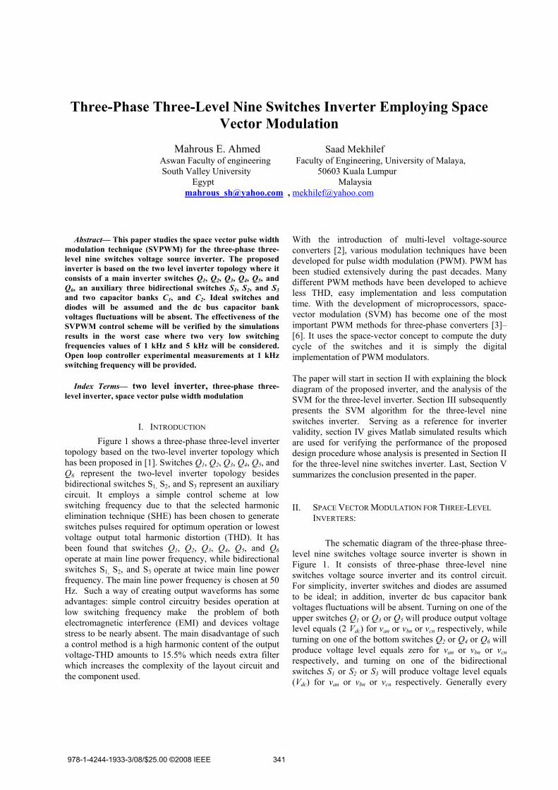
Figure 2 shows all the switching vectors of a
three-level (n = 3) multilevel inverter labeled with the position of the equivalent phase switches defined by the first part of equation (5). Note that the reference voltage vector *
REFV is represented by a circle; the radius of this
circ le is defined by *REFV .
Figure 1: The proposed three-phase three-level nine switches inverter
n
Q1 Q3 Q5
Q2 Q4 Q6
a
b
c S3
S2
S1
N
-
-
+
+
Vdc
Vdc
342
III. THE SPACE VECTOR MODULATION ALGORITHM FOR 3-LEVELS INVERTER
Based on algorthims explained in [7-8], switches ON/OFF states can be evaluated, the following steps summarizes this procedure. - First step is the normalization of the reference line-to-line space vector voltage as follows [7]:
dc
REFREF V
VnV )1()( nor −=
This normalization depends on the number of levels of the multilevel inverter n and the voltage level value of the dc bus capacitors Vdc. - Locating the region of the reference line-to-line refernce space vector, calculating the three nearest line-to-line switching voltages van vbn, and vcn, and their switching times are the second step [8]. Having evaluated van vbn, and vcn,, therefore ka, kb, and kc, and hence switches on/off state can be derived as follows for phase a:
⎪⎩
⎪⎨
⎧=
OFF isit otherwise ON0OFF isit otherwise ON1OFF isit otherwise ON2
2
1
1
QSQ
k a
Figure 3 illustrates the MALAB SIMULINK propgram to execute the aformentioned analysis that can generate switches states for inverter switches.
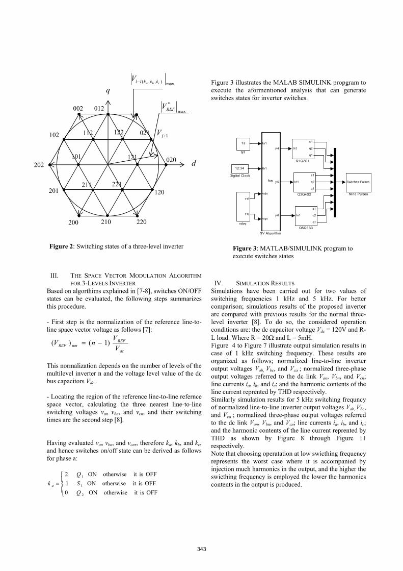
IV. SIMULATION RESULTS Simulations have been carried out for two values of switching frequencies 1 kHz and 5 kHz. For better comparison; simulations results of the proposed inverter are compared with previous results for the normal three-level inverter [8]. To do so, the considered operation conditions are: the dc capacitor voltage Vdc = 120V and R-L load. Where R = 20Ω and L = 5mH. Figure 4 to Figure 7 illustrate output simulation results in case of 1 kHz switching frequency. These results are organized as follows; normalized line-to-line inverter output voltages Vab, Vbc, and Vca ; normalized three-phase output voltages referred to the dc link Van, Vbn, and Vcn; line currents ia, ib, and ic; and the harmonic contents of the line current reprented by THD respectively. Similarly simulation results for 5 kHz switching frequncy of normalized line-to-line inverter output voltages Vab, Vbc, and Vca ; normalized three-phase output voltages referred to the dc link Van, Vbn, and Vcn; line currents ia, ib, and ic; and the harmonic contents of the line current reprented by THD as shown by Figure 8 through Figure 11 respectively. Note that choosing operatation at low swicthing frequency represents the worst case where it is accompanied by injection much harmonics in the output, and the higher the swicthing frequency is employed the lower the harmonics contents in the output is produced.
Figure 2: Switching states of a three-level inverter
q
d
1+jV
012 002
102
202
201
200 210 220
120
020
211 221
101 121
112 122 021
max
*REFV
max),,( cba kkkllV −
Figure 3: MATLAB/SIMULINK program to execute switches states
v d
v q
vdvq
Ts
ts1
ts1
th1
v dn
v qn
y 4
y 5
y 6
fcn
SV Algorithm
In1
s1
q2
q1
Q5Q6S3
In1
s1
q2
q1
Q3Q4S2
In1
s1
q2
q1
Q1Q2S1
Switches Pulses
Nine Pulses
12:34
Digital Clock
343
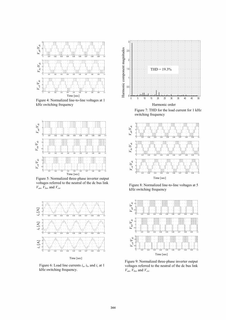
Figure 4: Normalized line-to-line voltages at 1 kHz switching frequency
0 0.01 0.02 0.03 0.04 0.05 0.06 0.07 0.08 0.09 0.1-2
0
2
0 0.01 0.02 0.03 0.04 0.05 0.06 0.07 0.08 0.09 0.1-2
-1
0
1
2
0 0.01 0.02 0.03 0.04 0.05 0.06 0.07 0.08 0.09 0.1-2
-1
0
1
2
V ab/V
dc
V bc/V
dc
V ca/V
dc
Time [sec]
Figure 5: Normalized three-phase inverter output voltages referred to the neutral of the dc bus link Van, Vbn, and Vcn.
0 0.01 0.02 0.03 0.04 0.05 0.06 0.07 0.08 0.09 0.10
1
2
0 0.01 0.02 0.03 0.04 0.05 0.06 0.07 0.08 0.09 0.10
0.5
1
1.5
2
0 0.01 0.02 0.03 0.04 0.05 0.06 0.07 0.08 0.09 0.10
0.5
1
1.5
2
V an/V
dc
V bn/V
dc
V cn/V
dc
Time [sec]
0 0.01 0.02 0.03 0.04 0.05 0.06 0.07 0.08 0.09 0.1-2
-1
0
1
2
0 0.01 0.02 0.03 0.04 0.05 0.06 0.07 0.08 0.09 0.1-2
-1
0
1
2
0 0.01 0.02 0.03 0.04 0.05 0.06 0.07 0.08 0.09 0.1-2
-1
0
1
2
Figure 8: Normalized line-to-line voltages at 5 kHz switching frequency
V ab/V
dc
V bc/V
dc
V ca/V
dc
Time [sec]
Figure 6: Load line currents ia, ib, and ic at 1 kHz switching frequency.
i a [A
] i b
[A]
i c [A
]
Time [sec]
0 0.01 0.02 0.03 0.04 0.05 0.06 0.07 0.08 0.09 0.1-4
-2
0
2
4
0 0.01 0.02 0.03 0.04 0.05 0.06 0.07 0.08 0.09 0.1-4
-2
0
2
4
0 0.01 0.02 0.03 0.04 0.05 0.06 0.07 0.08 0.09 0.1-4
-2
0
2
4
0 0.01 0.02 0.03 0.04 0.05 0.06 0.07 0.08 0.09 0.10
0.5
1
1.5
2
0 0.01 0.02 0.03 0.04 0.05 0.06 0.07 0.08 0.09 0.10
0.5
1
1.5
2
0 0.01 0.02 0.03 0.04 0.05 0.06 0.07 0.08 0.09 0.10
0.5
1
1.5
2
Figure 9: Normalized three-phase inverter output voltages referred to the neutral of the dc bus link Van, Vbn, and Vcn.
V an/V
dc
V bn/V
dc
V cn/V
dc
Time [sec]
0 5 10 15 20 25 30 35 40 45 500
0.5
1
1.5
2
2.5
3
Figure 7: THD for the load current for 1 kHz switching frequency
Har
mon
ic c
ompo
nent
mag
nitu
des
Harmonic order
THD = 19.3%
344

V. LABORATORIES MEASUREMENTS
The experiments were conducted using open-loop controller and the input DC inverter bus voltages are assumed to be fixed without fluctuations. A DSP TMS320F2812 board has been as a controller. Switches pulses generation program shown in Figure 3 runs in MATLAB and its results are downloaded and stored in the DSP board. Due to the speed limitations of the controller, results have been carried out only for the lowest switching frequency which is 1 kHz. the considered operation conditions are: each dc capacitor voltage Vdc = 60V , thus 120V on the inverter dc bus, static R-L load with R = 20Ω and L = 5mH, and fs = 1 kHz.
Figure 12 illustrates controlling pulses of inverter switches, for phase a, generated by DSP TMS320F2812 controller using the aforementioned procedure at 1 kHz switching frequency. Figure 13 illustrates the line-to-line voltage of Vab and Vca respectively, with 240V peak-to-peak and about 75V RMS. Figure 14 shows load phase voltages van, vbn, and vcn referred to the neutral of the DC bus voltage. Figure 15 shows the line currents ia, and ib, while Figure 16 shows the line currents ib, and ic. The output current harmonic contents at switching frequency 1 kHz is shown in figure 17. The simulation results and the laboratory measurements verify the effectiveness of the SVPWM control scheme for the proposed inverter
Figure 12: controlling pulses of Q1, S1, and Q2 switches respectively at 1 kHz switching frequency.
Figure 13 Line-to-line voltages Vab and Vbc at 1 kHz switching frequency (10msec/div, 100V/div).
V ab
V ca
Time [sec]
0 5 10 15 20 25 30 35 40 45 500
0.5
1
1.5
2
2.5
3
Figure 11: THD for the load current for 5 kHz switching frequency
Har
mon
ic c
ompo
nent
mag
nitu
des
Harmonic order
THD = 5.7%
Figure 10: Load line currents ia, ib, and ic at 5 kHz switching frequency.
i c [A
] i b
[A]
i a [A
]
Time [sec]
0 0.01 0.02 0.03 0.04 0.05 0.06 0.07 0.08 0.09 0.1-4
-2
0
2
4
0 0.01 0.02 0.03 0.04 0.05 0.06 0.07 0.08 0.09 0.1-4
-2
0
2
4
0 0.01 0.02 0.03 0.04 0.05 0.06 0.07 0.08 0.09 0.1-4
-2
0
2
4
345
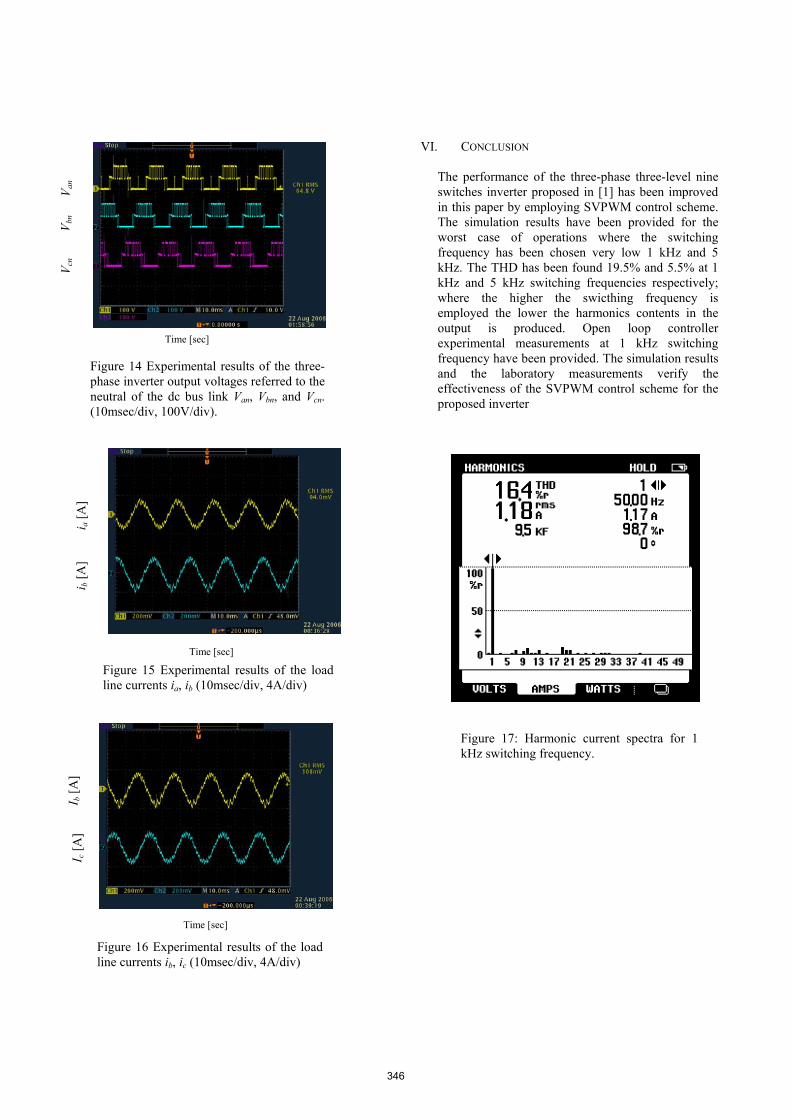
VI. CONCLUSION The performance of the three-phase three-level nine switches inverter proposed in [1] has been improved in this paper by employing SVPWM control scheme. The simulation results have been provided for the worst case of operations where the switching frequency has been chosen very low 1 kHz and 5 kHz. The THD has been found 19.5% and 5.5% at 1 kHz and 5 kHz switching frequencies respectively; where the higher the swicthing frequency is employed the lower the harmonics contents in the output is produced. Open loop controller experimental measurements at 1 kHz switching frequency have been provided. The simulation results and the laboratory measurements verify the effectiveness of the SVPWM control scheme for the proposed inverter
Figure 14 Experimental results of the three-phase inverter output voltages referred to the neutral of the dc bus link Van, Vbn, and Vcn. (10msec/div, 100V/div).
V an
V bn
V cn
Time [sec]
Figure 15 Experimental results of the load line currents ia, ib (10msec/div, 4A/div)
i b [A
] i a
[A]
Time [sec]
Figure 16 Experimental results of the load line currents ib, ic (10msec/div, 4A/div)
I c [A
] I b
[A]
Time [sec]
Figure 17: Harmonic current spectra for 1 kHz switching frequency.
346

REFERENCES:
[2] Mahrous, E.A.; Rahim, N.A.; Hew, W.P., “Three-
Phase Three-Level Voltage Source Inverter With Low Switching Frequency Based On The Two-Level Inverter Topology”, IET Proceedings-Electric Power Applications, Vol. 1, Issue 4, pp. 637-641, July 2007 .
[2] A. Nabae, I. Takahashi, and H. Akagi, “A new neutral-point clamped PWM inverter”, IEEE Transactions Industrial Applications, vol. 17, pp. 518–523, Sept./Oct. 1981.
[3] O. Ogasawara, H. Akagi, and A. Nabel, “A novel PWM scheme of voltage source inverters based on space vector theory,” in Proc. EPE European Conference on Power Electronics and Applications, pp. 1197–1202, 1989.
[4] J. Holtz, “Pulsewidth Modulation for Electronic Power Conversion”, Proceedings of the IEEE, Vol.82, Issue 8, August 1994, pp. 1194–1214.
[5] J. Holtz, W. Lotzkat, and A. Khambadkone, “On
continuous control of PWM inverters in the overmodulation range including the six-step mode,” in Proceedings of the IEEE IECON’92, pp. 307–312, 1992.
[6] B. K. Bose and H. A. Sutherland, “A high performance pulsewidth modulator for an inverter-fed drive system using a microcomputer,” IEEE Transaction Industrial Application, vol. 19, pp. 235–243, March/April 1983.
[7] Nikola Celanovic, and Dushan Boroyevich, “A Fast Space-Vector Modulation Algorithm for Multilevel Three-Phase Converters”, IEEE Transactions on Industry Applications, Vol. 37, Issue 2, pp. 637-641. March/April 2001.
[8] M. M. Prats, R. Portillo, J.M, Carrasco, L.G. Franquelo, “New Fast Space-Vector Modulation for Multilevel Converters Based on Geometrical Consideration”, Industrial Electronics Society, 28th Annual Conference of the IEEE, Vol. 4, pp. 3134-3139, 5-8 November 2002.
347