Three-DimensionalTopologicalInsulators … · Three-DimensionalTopologicalInsulators 3 physics that...
53
arXiv:1011.5462v1 [cond-mat.str-el] 24 Nov 2010 Three-Dimensional Topological Insulators 1 Three-Dimensional Topological Insulators M. Zahid Hasan Joseph Henry Laboratory, Department of Physics, Princeton University, Princeton, NJ 08544, and Princeton Center for Complex Materials, PRISM, Princeton University, Princeton, NJ 08544 Joel E. Moore Department of Physics, University of California, Berkeley, California 94720, and Materials Sciences Division, Lawrence Berkeley National Laboratory, Berkeley, California 94720 Key Words Topological insulators. Spin-orbit coupling. Surface states. Quan- tum Hall effect and topological phases. Abstract Topological insulators in three dimensions are nonmagnetic insulators that possess metallic surface states as a consequence of the nontrivial topology of electronic wavefunctions in the bulk of the material. They are the first known examples of topological order in bulk solids. We review the basic phenomena and experimental history, starting with the observation of topo- logical insulator behavior in BixSb1-x by spin- and angle-resolved photoemission spectroscopy and continuing through measurements on other materials and by other probes. A self-contained introduction to the single-particle theory is then given, followed by the many-particle definition of a topological insulator as a material with quantized magnetoelectric polarizability. The last
Transcript of Three-DimensionalTopologicalInsulators … · Three-DimensionalTopologicalInsulators 3 physics that...
arX
iv:1
011.
5462
v1 [
cond
-mat
.str
-el]
24
Nov
201
0
Three-Dimensional Topological Insulators 1
Three-Dimensional Topological Insulators
M. Zahid Hasan
Joseph Henry Laboratory, Department of Physics, Princeton University,
Princeton, NJ 08544, and Princeton Center for Complex Materials, PRISM,
Princeton University, Princeton, NJ 08544
Joel E. Moore
Department of Physics, University of California, Berkeley, California 94720, and
Materials Sciences Division, Lawrence Berkeley National Laboratory, Berkeley,
California 94720
Key Words Topological insulators. Spin-orbit coupling. Surface states. Quan-
tum Hall effect and topological phases.
Abstract Topological insulators in three dimensions are nonmagnetic insulators that possess
metallic surface states as a consequence of the nontrivial topology of electronic wavefunctions in
the bulk of the material. They are the first known examples of topological order in bulk solids.
We review the basic phenomena and experimental history, starting with the observation of topo-
logical insulator behavior in BixSb1−x by spin- and angle-resolved photoemission spectroscopy
and continuing through measurements on other materials and by other probes. A self-contained
introduction to the single-particle theory is then given, followed by the many-particle definition
of a topological insulator as a material with quantized magnetoelectric polarizability. The last
Annu. Rev. Condensed Matter 2010 1 00
section reviews recent work on strongly correlated topological insulators and new effects that
arise from the proximity effect between a topological insulator and a superconductor. While
this article is not intended to be a comprehensive review of what is already a rather large field,
we hope that it will serve as a useful introduction, summary of recent progress, and guideline
to future directions.
CONTENTS
INTRODUCTION . . . . . . . . . . . . . . . . . . . . . . . . . . . . . . . . . . . . 2
BASIC PHENOMENA AND EXPERIMENTS . . . . . . . . . . . . . . . . . . . . 5
INDEPENDENT-ELECTRON THEORY OF 3D TOPOLOGICAL INSULATORS 16
Time-reversal invariance in Fermi systems . . . . . . . . . . . . . . . . . . . . . . . . . 20
3D topological insulators . . . . . . . . . . . . . . . . . . . . . . . . . . . . . . . . . . . 24
TOPOLOGICAL INSULATORS AND ORBITAL MAGNETOELECTRIC POLAR-
IZABILITY . . . . . . . . . . . . . . . . . . . . . . . . . . . . . . . . . . . . . . . . 28
RECENTDEVELOPMENTS: STRONG CORRELATIONS ANDMAJORANA FERMIONS 32
1 INTRODUCTION
Condensed matter physics starts at microscopic scales with a clear notion of
spacetime distance defined by the Minkowski metric of special relativity. It has
been understood since the discovery of the integer quantum Hall effect (IQHE)
that some phases of matter, known as topological phases, reflect the “emergence”
of a different type of spacetime. The notion of a metric disappears entirely, and
macroscopic physics is controlled by properties that are insensitive to spacetime
distance and described by the branch of mathematics known as topology. The
emergence of a topological description reflects a type of order in condensed matter
2

Three-Dimensional Topological Insulators 3
physics that is quite different from conventional orders described in terms of
symmetry breaking. This review discusses recent experimental and theoretical
progress on three-dimensional topological insulators, the first topological phase
of bulk solids.
One distinguishing feature of topological phases is that they are typically insu-
lating or “gapped” in bulk but possess gapless edge or surface states as a result
of the topology. A related property is that the topological order can lead to
measurable physical properties with extremely precise quantization as a result of
the insensitivity of topology to local perturbations such as defects and thermal
fluctuations; the first example was the Hall (i.e., transverse) conductance in the
IQHE, which can be quantized to an integer multiple of e2/h with an accuracy of
one part per billion. However, topological order until recently was only observed
in two-dimensional electron gases under extreme conditions of low temperature
and high magnetic field.
The current excitement in this field results from the experimental discovery
that there are topological phases in fairly ordinary materials that occur in three
dimensions and zero magnetic field (1, 2, 3). The existence of three-dimensional
(3D)“ topological insulators” (4) was predicted by deriving topological invari-
ants for a general time-reversal-invariant band insulator that built on previous
work (5) on a new topological invariant of time-reversal-invariant band insulators
in 2D. Topological invariants are mathematical quantities, in this case essentially
integrals over a band structure, that are stable to continuous changes of param-
eters. Simpler forms of these invariants in inversion-symmetric materials were
found independently (6) and used to predict the first topological insulator to be
discovered, BixSb1−x (7). The 2D topological invariant underlies the “quantum

4 Hasan & Moore
spin Hall effect” observed in quantum wells derived from HgTe (8,9). The general
term “topological insulators” was coined to indicate that both the 2D and 3D
phases are topological in the same sense as the IQHE, with topologically pro-
tected edge or surface states that result from spin-orbit coupling rather than a
magnetic field.
The method used to discover all 3D topological insulators known so far is angle-
resolved photoemission spectroscopy (ARPES), which probes directly the unique
metallic surface state and consequently the topological invariants. The accessi-
bility of 3D topological insulators to a variety of experimental probes means that
many other types of data are now available. Topological insulators in several ma-
terials families have been discovered to date, and theoretical work has connected
topological insulators to many other areas of condensed matter physics. As both
technical (2) and non-technical (10,3) reviews are available that introduce three-
dimensional topological insulators following the historical development from the
2D case, and there is a published review specifically on the 2D case (9, 11), we
seek here to give a reasonably self-contained treatment of the 3D case, which is
the focus of most current interest for both practical and fundamental reasons.
Given length limitations and the existing review of the literature as of early
2010 (2), we will seek here to give an overview of basic facts and the essential theo-
retical background, then concentrate on recent developments. We first review the
basic facts and experimental discoveries in Section II. This section includes a dis-
cussion of which materials are currently believed to be topological insulators and
how these materials are characterized by various techniques. Our discussion of
the theory of topological insulators and how they connect to several long-standing
projects of theoretical physics, makes up Section III. Discussing even a few as-
Three-Dimensional Topological Insulators 5
pects in depth means that there are omissions in other areas; in particular, we will
have little to say in Section III about other topological single-particle problems
such as the quasiparticle Hamiltonians of topological superconductors (12,13).
Recent developments show that some important features of the 3D topological
insulator can be understood in terms of the orbital contribution to magnetoelec-
tric polarizability (Section IV), and more directly derived directly in 3D, or even
by working down from 4D, than by working up from 2D; in this respect our dis-
cussion reflects later improvements in theoretical understanding. Some rapidly
developing areas are reviewed in Section V, such as proposed proximity effects
between superconductors and topological insulators.
2 BASIC PHENOMENA AND EXPERIMENTS
This section summarizes the current body of experimental knowledge on 3D topo-
logical insulators. Readers seeking to understand the theoretical background of
the experimental observations may wish to consult Section III in parallel. The
first 3D topological insulator to be experimentally discovered was the semicon-
ducting alloy Bi1−xSbx, whose unusual surface bands were mapped in an angle-
resolved photoemission (ARPES) experiment. ARPES uses a photon to eject an
electron from a crystal, then determines the surface or bulk electronic structure
from an analysis of the momentum of the emitted electron. The 3D topological
state in Bi1−xSbx is a new state in the sense that it cannot be reduced to a
quantum spin Hall state (4, 6, 14). Its surface is a new form of 2D metal where
electron’s spin and linear momentum are locked one to one and the two dimen-
sional Fermi surface carries a nontrivial Berry’s phase of π (6). Its uniqueness
can be understood in the following way : a layered three dimensional version
6 Hasan & Moore
of the quantum spin Hall insulator Hg(Cd)Te would be a ”weak 3D topological
insulator (WTI)” with invariant structure of (νo=0,111). A WTI would exhibit
surface states that contain even number of Dirac cones thus a net Berry’s phase
of 0 or 2π. The surface states of a WTI are not robust against disorder.
Unlike in a transport experiment, ARPES carried out in a spin resolution
mode can, in addition, measures the distribution of spin orientations on the
Fermi surface which can be used to estimate the Berry’s phase on the surface.
Spin sensitivity is critically important for probing the existence spin-momentum
locking on the surface expected as a consequence of bulk topological order. The
3D topological insulator Bi1−xSbx on the other hand have odd number of surface
states whose spin-texture supports a non-trivial Berry’s phase providing protec-
tion against non-magnetic disorder. Such a topological insulator is described by
(νo=1, ~M).
Bismuth antimony alloys have long been studied for their thermoelectric prop-
erties (16). Bismuth is a semimetal with strong spin-orbit interactions. Its band
structure features an indirect negative gap between the valence band maximum
at the T point of the bulk Brillouin zone (BZ) and the conduction band min-
ima at three equivalent L points (17). The valence and conduction bands at
L are derived from antisymmetric (La) and symmetric (Ls) p-type orbitals, re-
spectively, and the effective low-energy Hamiltonian at this point is described by
the (3+1)-dimensional relativistic Dirac equation (18). The resulting dispersion
relation, E(~k) = ±√
(~v · ~k)2 +∆2 ≈ ~v · ~k, is highly linear owing to the com-
bination of an unusually large band velocity ~v and a small gap ∆ (such that
|∆/|~v|| ≈ 5× 10⁻³A−1) and has been used to explain various peculiar properties
of bismuth. Substituting bismuth with antimony changes the critical energies of
Three-Dimensional Topological Insulators 7
the band structure. At an Sb concentration of x ≈ 4%, the gap ∆ between La and
Ls closes and a massless three-dimensional (3D) Dirac point is realized. As x is
further increased this gap re-opens with inverted symmetry ordering, which leads
to a change in sign of ∆ at each of the three equivalent L points in the BZ. For
concentrations greater than x > 7% there is no overlap between the valence band
at T and the conduction band at L, and the material becomes an inverted-band
insulator. Once the band at T drops below the valence band at L, at x ≈ 7%, the
system evolves into a direct-gap insulator with a massive Dirac-like bulk bands.
Although the presence of bulk and surface states in Bi-based materials were
known, experiments by Hsieh et.al. (1) establish the existence of a direct energy
gap in the bulk Dirac-like band-structure of Bi0.9Sb0.1. The linearly dispersive
bulk bands are uniquely consistent with strong spin-orbit coupling nature of the
inverted insulator. The same experiments observed several non-degenerate sur-
face states that span the bulk gap. In general, the states at the surface of spin-
orbit coupled compounds are allowed to be spin split owing to the loss of space
inversion symmetry [E(k, ↑) = E(−k, ↑)]. However, as required by Kramers’ the-
orem, this splitting must go to zero at the four time reversal invariant momenta
(TRIM) in the 2D surface BZ as required by Kramers theorem. Along a path
connecting two TRIM in the same BZ, the Fermi energy inside the bulk gap will
intersect these singly degenerate surface states either an even or odd number of
times. When there are an even number of surface state crossings, the surface
states are topologically trivial because weak disorder (as may arise through al-
loying) or correlations can remove pairs of such crossings by pushing the surface
bands entirely above or below EF . When there are an odd number of crossings,
however, at least one surface state must remain gapless, which makes it non-
8 Hasan & Moore
trivial. Such “topological metal” surface states cannot be realized in a purely 2D
electron gas system such as the one realized at the interface of GaAs/GaAlAs or
on the surface of Si.
On the (111) surface of Bi0.9Sb0.1, the four TRIM are located at Γ and three
M points that are rotated by 60 relative to one another. Owing to the three-fold
crystal symmetry (A7 bulk structure) and the mirror symmetry of the surface
Fermi surface across kx = 0, these three M points are equivalent. In pure bismuth
(Bi), two surface bands emerge from the bulk band continuum near Γ to form a
central electron pocket and an adjacent hole lobe. These two bands result from
the spin-splitting of a surface state and are thus singly degenerate. In Bi-Sb
alloy, in addition, a narrow electron pocket which is doubly degenerate around
M is also observed (Fig.1). This is indicated by its splitting below EF between
−kx ≈ 0.55A−1 and M , as well as the fact that this splitting goes to zero at
M in accordance with Kramers theorem. In Bi0.9Sb0.1, the states near M fall
completely inside the bulk energy gap preserving their purely surface character
at M unlike in Bi. The surface Kramers point is located approximately 15 ± 5
meV below EF at ~k = M . The observation of five surface state crossings (an odd
rather than an even number) between Γ and M , confirmed by the observation
of the Kramers degenerate point confirms the topologically non-trivial nature of
the material. While these results are consistent with a Z2 topological insulator
scenario for Bi-Sb, more decisive evidence comes from the study of spin-texture
of the surface Fermi surface.
The bulk topological Z2 order is expected to give rise to unusual spin physics
at the edges or surfaces of topological insulators. However, unlike quantum Hall
systems, the topological insulator surfaces do not necessarily exhibit a quantized
Three-Dimensional Topological Insulators 9
charge or spin response. In fact, the spin polarization is not a conserved quantity
in a spin-orbit material. Thus, their topological quantum numbers, the analogs
of the Chern number, cannot be measured via the classic magneto-transport
methods. ARPES with spin sensitivity can perform analogous measurements for
topological insulators by mapping out all 4 topological quantum numbers that
uniquely identify the topological class. Hsieh et.al. (19) measured the topological
numbers for Bi1−xSbx and provided an identification of its spin texture, which
heretofore was unmeasured despite its surface states (SSs) having been observed.
The measured spin texture (Fig.2) reveals the existence of a nonzero geometrical
quantum phase, a Berry’s phase of π and the handedness or chiral properties.
Spin-ARPES technique enables to investigate aspects of the metallic regime of
the Bi1−xSbx series, such as spin properties in pure Sb, which are necessary to de-
termine the microscopic origin of topological order. Spin-ARPES measurements
on Sb showed that its surface carries a geometrical (Berry’s) phase and chirality
property unlike the conventional spin-orbit metals such as gold, which has zero
net Berry’s phase and no net chirality.
The odd number of Fermi crossings protects the topological surface from be-
coming insulating, regardless of the position of the chemical potential or the influ-
ence of non-magnetic perturbations. Spin-ARPES experiments have established
that these surface states have a chiral spin structure and carries a non-trivial
Berry’s phase, which makes them distinct from ordinary surface states. All these
characteristics suggest that backscattering, or scattering between states of equal
and opposite momentum, which results in Anderson localization in typical low-
dimensional systems (24), will not occur for these two-dimensional carriers. Ran-
dom alloying in Bi1−xSbx, which is not present in other material families of topo-
10 Hasan & Moore
logical insulators found to date, makes this material system an ideal candidate
in which to examine the impact of disorder or random potential on topological
surface states. The fact that the chiral two-dimensional states are indeed pro-
tected from spin-independent scattering was established by Roushan et.al. (20)
by combining results from scanning tunneling spectroscopy (STM/STS) and spin-
ARPES on Bi0.92Sb0.08. The results show that despite strong atomic scale disor-
der and random potential, elastic-backscattering between states of opposite mo-
mentum and opposite spin is absent. These observations demonstrate that the
chiral nature of these states protects the spin of the carriers which is ultimately a
consequence of time-reversal symmetry. The same conclusion has emerged from
studies of the electronic interference patterns near defects or steps on the surface
that electrons never turn completely around when scattered in other topological
insulators (25,26)).
While the surface structure of Bi1−xSbx alloy material was found to be rather
complicated and bandgap to be rather small, this work launched a search for
topological insulators with larger bandgap and simpler surface spectrum for ob-
serving topological phenomena at high temperatures. Topological phenomena
in materials are usually very fragile and impossible to create without liquid he-
lium temperatures and high magnetic fields. New three-dimensional ”topological
insulator” materials, especially Bi2Se3, offer the potential for protected surface
states and other topological behavior at room temperature. In 2008, work led
by a Princeton group used angle-resolved photoemission spectroscopy (ARPES)
and first-principles calculations to study the surface band structure of Bi2Se3
and observe the characteristic signature of a topological insulator in the form of
a single-Dirac-cone (21,22). Concurrent theoretical work by H.Zhang et al. (27)
Three-Dimensional Topological Insulators 11
used electronic structure methods to show that Bi2Se3 is just one of several new
large-bandgap topological insulators. Zhang et.al., also provided a simple tight-
binding model to capture the single-Dirac-cone observed in Bi2Te3 (28) and made
new predictions about Bi2Se3 and Sb2Te3. Subsequently, detailed and systematic
surface investigations of Bi2Se3 (23,29,30); Bi2Te3 (31,23,32,33) and Sb2Te3 (32)
confirmed the topological band-structure of all 3 of these materials.
The unusual planar metal that forms at the surface of topological insulators
inherits topological properties from the bulk bandstructure. The manifestation of
this bulk-surface connection occurs at a smooth surface where momentum along
the surface remains well-defined: in its simplest possible form, each momentum
along the surface has only a single spin state at the Fermi level, and the spin
direction rotates as the momentum moves around the Fermi surface ensuring a
non-trivial Berry’s phase. These two defining properties of topological insulators
namely spin-momentum locking of surface states and π Berry’s phase along with
the consequences such as the robustness to non-magnetic disorder could be most
clearly demonstrated with the discovery of the second generation of topological
insulators.
While the phase observed in Bi1−xSbx alloys is theoretically the same as that
observed in the Bi2Se3 class, there are three crucial differences that suggest that
this series may become the reference material for future experiments on this
phase. The Bi2Se3 surface state is found from ARPES and theory to be nearly
the idealized single Dirac cone as seen from the experimental data in Fig.4&5.
Second, Bi2Se3 is stoichiometric (i.e., a pure compound rather than an alloy like
Bi1−xSbx) and hence can be prepared in principle at higher purity. While the
topological insulator phase is predicted to be quite robust to disorder, many
12 Hasan & Moore
experimental probes of the phase, including ARPES of the surface band struc-
ture, are clearer in high-purity samples. Finally, and perhaps most important
for applications, Bi2Se3 has a large band gap of approximately 0.3 eV (equiv-
alent to 3600 Kelvin). In its high purity form, the large band gap of Bi2Se3
indicates that topological behavior can be seen at room temperature and greatly
increases the potential for applications (Fig.7). To understand the likely impact
of these new topological insulators, an analogy can be drawn with the early days
of high-temperature cuprate superconductivity: the original cuprate supercon-
ductor LBCO was quickly superseded by ”second-generation” materials such as
YBCO and BSCCO for most applied and scientific purposes (34).
All the key properties of topological states have been demonstrated for Bi2Se3
which has the most simple Dirac cone surface spectrum and the largest band-
gap (0.3 eV). In Bi2Te3 the surface states exhibit large deviations from a simple
Dirac cone due to a combination of smaller band-gap (0.15 eV) and a strong
trigonal potential (31) which can be utilized to explore some aspects of its surface
properties (36, 37). Hexagonal deformation of the surface states is confirmed by
STM measurements (26). Speaking of applications within this class of materials,
Bi2Te3, is already well known to materials scientists working on thermoelectricity:
it is a commonly used thermoelectric material in the crucial engineering regime
near room temperature.
Two defining properties of topological insulators namely spin-momentum lock-
ing of surface states and π Berry’s phase could be clearly demonstrated in Bi2X3
series. The protected nature of the surface states are also most straightforwardly
demonstrated. Topological surface states are protected by time reversal symme-
try which implies that the surface state Dirac node would be robust in the pres-
Three-Dimensional Topological Insulators 13
ence of non-magnetic disorder but open a gap in the presence of time-reversal
breaking perturbation of the system such as the effect of magnetic impurities and
the associated disorder. Magnetic impurity such as Fe on the surface of Bi2Se3
opens a gap at the Dirac point (Fig.5) (22,23,38). The magnitude of the gap is
likely set by the interaction of Fe ions with the Se surface and the time-reversal
breaking disorder potential introduced on the surface. Non-magnetic disorder
created via molecular absorbent NO2 or alkali atom adsorption (K or Na) on the
surface leaves the Dirac node intact (Fig.5) in both Bi2Se3 and Bi2Te3 (33, 23).
These results are consistent with the fact that the topological surface states are
protected to be metallic by time-reversal symmetry.
Most of the interesting theoretical proposals that utilize topological insulator
surfaces require the chemical potential to lie at the degenerate Dirac node similar
to the case in graphene. In graphene, the chemistry of carbon atoms naturally
locates the Fermi level at the Dirac point — the point at which the two cones in-
tersect — where the density of states vanishes. This makes its density of carriers
highly tunable by an applied electrical field and enables applications of graphene
to both basic science and microelectronics. The surface Fermi level of a topolog-
ical insulator does not have any particular reason to sit at the Dirac point, but
by a combination of surface and bulk chemical modification, tuning to the Dirac
point in Bi2Se3 was demonstrated by Hsieh et.al. (23). This was achieved by
passivating the Se vacancies with Ca in the bulk to place the Fermi level within
the bulk bandgap and then hole doping the surface with NO2 to keep the chem-
ical potential at the Dirac point. While this is an important advancement for
furthering the spectroscopic measurements, it needs to be seen how such a degree
of surface engineering can be achieved in a transport measurement geometry.
14 Hasan & Moore
Recent observations of superconductivity in CuxBi2Se3 (Tc = 3.8K) by Hor
et.al., (39) have raised interest in understanding the role of spontaneously bro-
ken symmetry within a topological band-structure. Measurements of electronic
band structure in CuxBi2Se3 (x=0 to 12%) by Wray et.al., (40) suggest that su-
perconductivity occurs with electrons in a bulk relativistic kinematic regime and
we identify that an unconventional doping mechanism causes the nontrivial topo-
logical surface character of the undoped compound to be preserved at the Fermi
level of the superconducting compound, where Cooper pairing occurs. Moreover,
they report key band parameters that constrain the form of the superconducting
state. These experimental observations provide important clues for developing
a theory of superconductivity in doped Bi-based topological insulators. Two
possible theoretical scenarios are shown in Fig.6.
While the 3D topological insulators, whose variants can host magnetism and su-
perconductivity, has generated widespread research activity in condensed-matter
and materials-physics communities, there has also been intense efforts to discover
new materials class. This is largely because some of the most interesting topolog-
ical phenomena, however, require topological insulators to be placed in multiply
connected, highly constrained geometries with magnets and superconductors all
of which thus require a large number of functional variants with materials design
flexibility as well as electronic, magnetic and superconducting tunability. Given
the optimum materials, topological properties open up new vistas in spintron-
ics, quantum computing and fundamental physics. We have extended the search
for topological insulators from the binary Bi-based series to the ternary thermo-
electric Heusler compounds. It has been recently found that although a large
majority of the well-known Heuslers such as TiNiSn and LuNiBi are rather topo-
Three-Dimensional Topological Insulators 15
logically trivial, the distorted LnPtSb-type (such as LnPtBi or LnPdBi, Ln=fn
lanthanides) compounds belonging to the half-Heusler subclass harbour Z2=-1
topological insulator parent states, where Z2 is the band parity product index.
Half-Heuslers provide a new platform for deriving a host of topologically exotic
compounds and their nanoscale or thin-film device versions through the inherent
flexibility of their lattice parameter, spinorbit strength and magnetic moment
tunability paving the way for the realization of multifunctional topological de-
vices (35,41). Heuslers are not insulating in their native state but growing them
on substrates making thinfilms or quantum-well structures provide a way to open
a band-gap turning them into real insulators.
While in the above we have focused on crystals for basic characterization,
films and nanostructures of topological insulators will eventually be important for
applications and have already enabled important tests of theoretical predictions.
Two examples are the observation of a thickness-dependent gap in MBE-grown
films (42) using in-situ ARPES and the transport measurement of Aharonov-
Bohm oscillations in topological insulator nanoribbons (43) (for the latter, see also
the theoretical works (44,45)). In addition to applications to thermoelectrics and
spintronics (46), such thin films might enable observation of an unusual exciton
condensate (47). The main remaining limitation of current materials, especially
for experimental techniques that (unlike ARPES) do not distinguish directly
between bulk and surface states, is that they have some residual conduction
in the bulk from impurity states even if the band-structure features an energy
gap.
16 Hasan & Moore
3 INDEPENDENT-ELECTRON THEORY OF 3D TOPOLOG-
ICAL INSULATORS
One view of topological insulators is that they represent a continuation, and
possibly the culmination, of a long-term program, initiated by David Thouless
and collaborators (48), to understand the consequences of the Berry phase for
electrons in solids. Their first result, even before the work by Berry that explained
the general concept of the Berry phase (49), related the topology of electron
wavefunctions in the to the integer quantum Hall effect. Topological phases
in which a response function is expressed in terms of a topological invariant are
often referred to as “Thouless-type topological phases”; the IQHE and topological
insulators in 2D and 3D are examples.
The integer quantum Hall effect has the remarkable property that, even at
finite temperature in a disordered material, a transport quantity is quantized to
remarkable precision: the transverse (a.k.a. Hall) conductivity is σxy = ne2/h,
where n is integral to 1 part in 109. This quantization results because σxy is deter-
mined by a topological invariant, and understand this intrinsically 2D topological
invariant also leads to the modern theory of polarization, which is mathemati-
cally a 1D quantity (i.e., it exists in dimensions 1 and above). We review these
developments in order to understand the single-particle picture of 3D topological
insulators and the connection to orbital magnetoelectric polarizability. Our dis-
cussion starts with noninteracting electrons in a perfect crystal and then explain
the generalizations to disorder and interactions.
In the IQHE and topological insulators, the topological invariant can be ob-
tained from integration over the Brillouin zone of a quantity derived from the
Berry phase of electron wavefunctions. The idea of the Berry phase (49) is that,
Three-Dimensional Topological Insulators 17
as an eigenstate evolves under a Hamiltonian whose parameters change adiabat-
ically, there is a physically significant phase that accumulates. The Berry phase
can be rather important even when it is not part of a topological invariant. In
crystalline solids, the electrical polarization, the anomalous Hall effect, and one
part of the magnetoelectric polarizability all derive from “non-topological” Berry
phases of the Bloch electron states.
The space of parameters for these Berry phases is just the crystal momentum
k: Bloch’s theorem for electrons in a periodic potential states that, given a po-
tential invariant under a set of lattice vectors R, V (r+R) = V (r), the electronic
eigenstates can be labeled by a “crystal momentum” k and written in the form
ψk(r) = eik·ruk(r), (1)
where the function u has the periodicity of the lattice. Note that the crystal
momentum k is only defined up to addition of reciprocal lattice vectors, i.e.,
vectors whose dot product with any of the original lattice vectors is a multiple of
2π.
While the energetics of Bloch wavefunctions (“band structure”) underlies many
properties of solids, and matrix elements of the wavefunctions are important for
optical and other properties, it has been appreciated only recently that many
phenomena are governed by Berry-phase physics arising from the smooth depen-
dence of the wavefunction uk on k. Even in a one-dimensional system, there is
a nontrivial “closed loop” in the parameter k that can be defined because of the
periodicity of the “Brillouin zone”’ k ∈ [−π/a, π/a):
γ =
∮ π/a
−π/a〈uk|i∂k|uk〉dk. (2)
Like other Berry phases, the phase γ is obtained as an integral of a “connection”

18 Hasan & Moore
A = 〈uk|i∂k|uk〉. In this 1D example, A is just a scalar; in higher dimensions it
is a vector potential that lives in momentum space. How are we to interpret this
Berry phase physically? An intuitive clue is provided if we make the replacement
i∂k by x, as would be appropriate if we consider the action on a plane wave.
This suggests, correctly, that the Berry phase may have something to do with
the spatial location of the electrons: in fact the electronic polarization is just
eγ/2π (50).
Another clue to what the phase γ might mean physically is provided by asking
if it is gauge-invariant. In the usual situation, gauge-invariance of the Berry phase
results from assuming that the wavefunction could be continuously defined on the
interior of the closed path. But here we have a closed path on a noncontractible
manifold; the path in the integral winds around the Brillouin zone, which has
the topology of the circle. (Here we are implicitly introducing another kind of
topological invariant. One kind comes from integrating differential forms derived
from the Berry phase, which is a “cohomology” invariant; another kind are “ho-
motopy” invariants, the generalizations of the notion of winding number. The
homotopy groups πn(M), which describe equivalence classes of mappings from
the sphere Sn to the manifold M , will occasionally be mentioned in technical
remarks below. The book of Nakahara (51) is a physics-oriented reference that
covers both cohomology and homotopy.)
What happens to the Berry phase if we introduce a phase change φ(k) in the
wavefunctions, |uk〉 → e−iφ(k)|uk〉, with φ(π/a) = φ(−π/a) + 2πn, n ∈ Z? Under
this transformation, the integral shifts as
γ → γ +
∮ π/a
−π/a(∂kφ) dk = γ + 2πn. (3)
So redefinition of the wavefunctions shifts the Berry phase, and this corresponds
Three-Dimensional Topological Insulators 19
to changing the polarization by a multiple of the “polarization quantum”, which
in one dimension is just the electron charge. (In higher dimensions, the po-
larization quantum of a crystal is one electron charge per transverse unit cell.)
Physically the ambiguity of polarization corresponds to how adding an integer
number of charges to one allowed termination gives another allowed termina-
tion (52). The Berry phase is not gauge-invariant, but any fractional part it had
in units of a is gauge-invariant. We discussed this one-dimensional example in
some detail because topological insulators will be very similar. The above calcula-
tion suggests that, to obtain a fully gauge-invariant quantity, we need to consider
a two-dimensional crystal rather than a one-dimensional one. Then integrating
the Berry curvature, rather than the Berry connection, has to give a well-defined
gauge-invariant quantity.
Indeed, the one-dimensional polarization example is related to the two-dimensional
integer quantum Hall effect, which historically came first. When a lattice is put in
a commensurate magnetic field (one with rational flux per unit cell, in units of the
flux quantum so that Bloch’s theorem applies), each occupied band j contributes
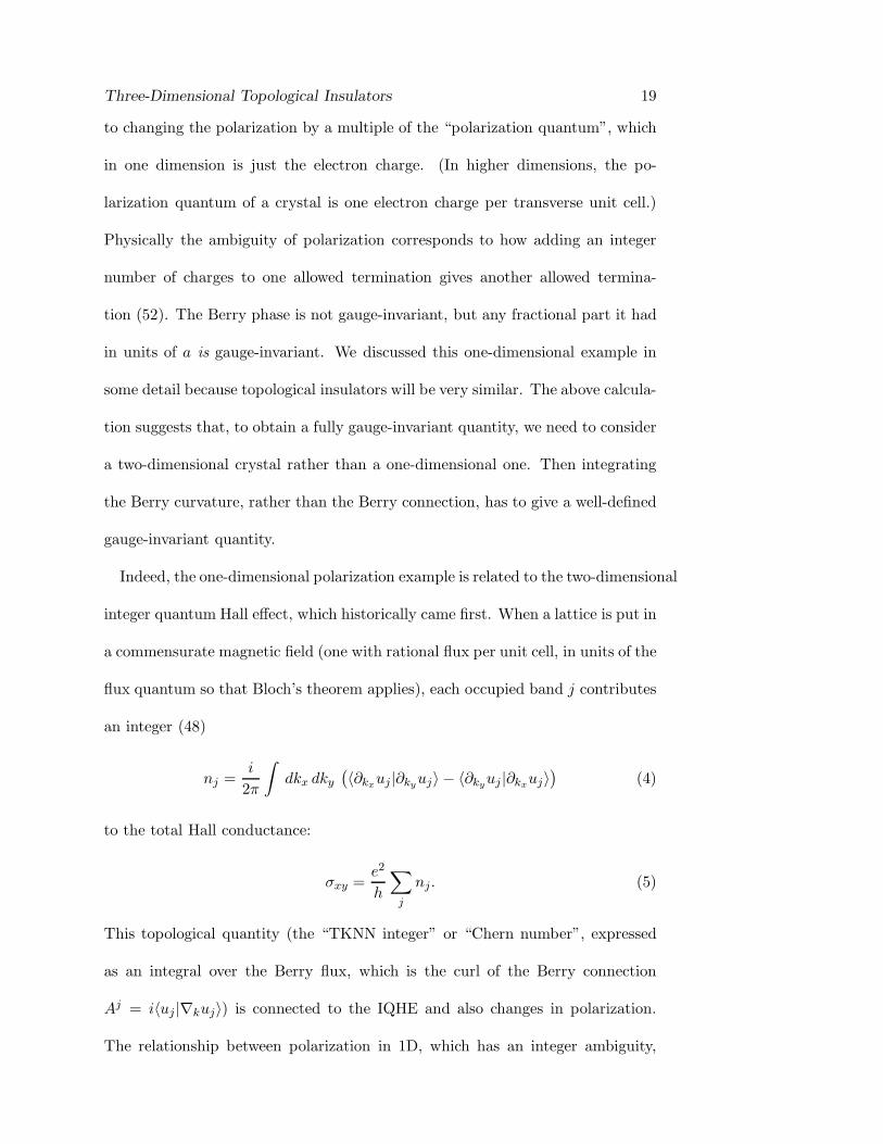
an integer (48)
nj =i
2π
∫
dkx dky(
〈∂kxuj|∂kyuj〉 − 〈∂kyuj |∂kxuj〉)
(4)
to the total Hall conductance:
σxy =e2
h
∑
j
nj. (5)
This topological quantity (the “TKNN integer” or “Chern number”, expressed
as an integral over the Berry flux, which is the curl of the Berry connection
Aj = i〈uj |∇kuj〉) is connected to the IQHE and also changes in polarization.
The relationship between polarization in 1D, which has an integer ambiguity,

20 Hasan & Moore
and the IQHE in 2D, which has an integer quantization, is the simplest example
of the relationship between Chern-Simons forms in odd dimension and Chern
forms in even dimension. Looking ahead, the topological insulator in 3D can be
similarly related to the topological invariants in 4 dimensions (53) that underlie
the “four-dimensional quantum Hall effect” (54).
One might worry whether the TKNN integer defined in equation (4) is specific
to noninteracting electrons in perfect crystals. An elegant way to generalize
the definition physically, while keeping the same mathematical structure, was
developed by Niu, Thouless, and Wu (55). One can imagine a disordered system
on a torus and rewrite the topological invariant above in terms of how much
charge is “pumped” around one circle by adiabatic insertion of flux through
the other circle. The same trick can be used to generalize the 3D topological
insulator invariants described below to disordered systems. While for the IQHE
the “flux trick” is sufficient to handle interacting systems as well as disordered
ones, a different approach is necesary for topological insulators. One final note
before moving on to time-reversal-invariant Fermi systems is that, while we have
concentrated above on giving explicit expressions for the invariants in terms of
wavefunctions, which is useful to get their physical meaning, it is often more
direct for topological classification to consider homotopy groups of the Bloch
Hamiltonians (56,53).
3.1 Time-reversal invariance in Fermi systems
Kane and Mele showed in 2005 that imposing time-reversal symmetry in 2D
electronic systems leads to new topological invariants. (57) While nonzero Chern
numbers cannot be realized with time-reversal invariance, the zero-Chern-number
Three-Dimensional Topological Insulators 21
class of systems gets subdivided into two pieces: “ordinary” insulators that do not
in general have an edge state, and a “quantum spin Hall effect” or “topological
insulator” where a bulk topological invariant forces an edge state. The topological
invariant is not an integer but rather a two-valued or Z2 invariant.
One idea that triggered this development was to consider two copies of the
quantum Hall effect, one for spin-up electrons and one for spin-down, with op-
posite effective magnetic fields for the two spins. This combination (58) is time-
reversal invariant because acting with the time-reversal operator T changes both
the magnetic field direction and the spin. Note that in a model such as this, Sz
is a conserved quantum number even though SU(2) (spin-rotation invariance) is
clearly broken, as up and down spins behave differently. Heuristically, think of
the spin-orbit coupling as arising from intra-atomic terms like L ·S, and consider
specifically LzSz. For an electron of fixed spin, this coupling to the orbital mo-
tion described by Lz is just like the coupling in a constant magnetic field. In the
simplest case of a Chern number +1 state of up electrons and a Chern number
−1 state of down electrons, the edge will have counterpropagating modes: e.g.,
up-spin moves clockwise along the edge and down-spin moves counterclockwise.
This turns out not to be a bad caricature of the quantum spin Hall phase in a
more realistic system: one can tell by symmetry arguments that it will have no
quantum Hall effect (i.e., αc = 0 in Ji = αcǫijkEjBk), but it will generically have
a “spin Hall effect”
J ij = αsǫijkEk, (6)
where αc and αs are numbers and J ij is a spin current (a current of angular
momentum i in spatial direction j).
As an example of this “two copies of the IQHE” generated by spin-orbit cou-
22 Hasan & Moore
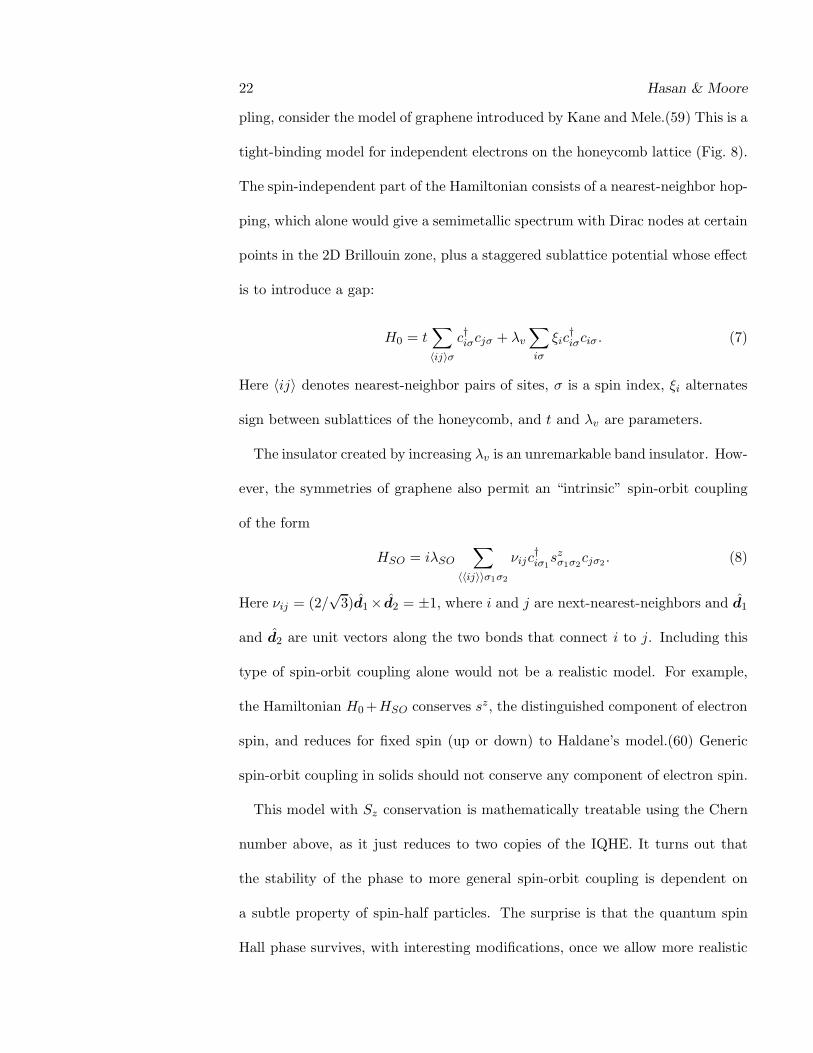
pling, consider the model of graphene introduced by Kane and Mele.(59) This is a
tight-binding model for independent electrons on the honeycomb lattice (Fig. 8).
The spin-independent part of the Hamiltonian consists of a nearest-neighbor hop-
ping, which alone would give a semimetallic spectrum with Dirac nodes at certain
points in the 2D Brillouin zone, plus a staggered sublattice potential whose effect
is to introduce a gap:
H0 = t∑
〈ij〉σ
c†iσcjσ + λv∑
iσ
ξic†iσciσ . (7)
Here 〈ij〉 denotes nearest-neighbor pairs of sites, σ is a spin index, ξi alternates
sign between sublattices of the honeycomb, and t and λv are parameters.
The insulator created by increasing λv is an unremarkable band insulator. How-
ever, the symmetries of graphene also permit an “intrinsic” spin-orbit coupling
of the form
HSO = iλSO∑
〈〈ij〉〉σ1σ2
νijc†iσ1szσ1σ2
cjσ2. (8)
Here νij = (2/√3)d1× d2 = ±1, where i and j are next-nearest-neighbors and d1
and d2 are unit vectors along the two bonds that connect i to j. Including this
type of spin-orbit coupling alone would not be a realistic model. For example,
the Hamiltonian H0+HSO conserves sz, the distinguished component of electron
spin, and reduces for fixed spin (up or down) to Haldane’s model.(60) Generic
spin-orbit coupling in solids should not conserve any component of electron spin.
This model with Sz conservation is mathematically treatable using the Chern
number above, as it just reduces to two copies of the IQHE. It turns out that
the stability of the phase to more general spin-orbit coupling is dependent on
a subtle property of spin-half particles. The surprise is that the quantum spin
Hall phase survives, with interesting modifications, once we allow more realistic
Three-Dimensional Topological Insulators 23
spin-orbit coupling, as long as time-reversal symmetry remains unbroken. The
time-reversal operator T acts differently in Fermi and Bose systems, or more
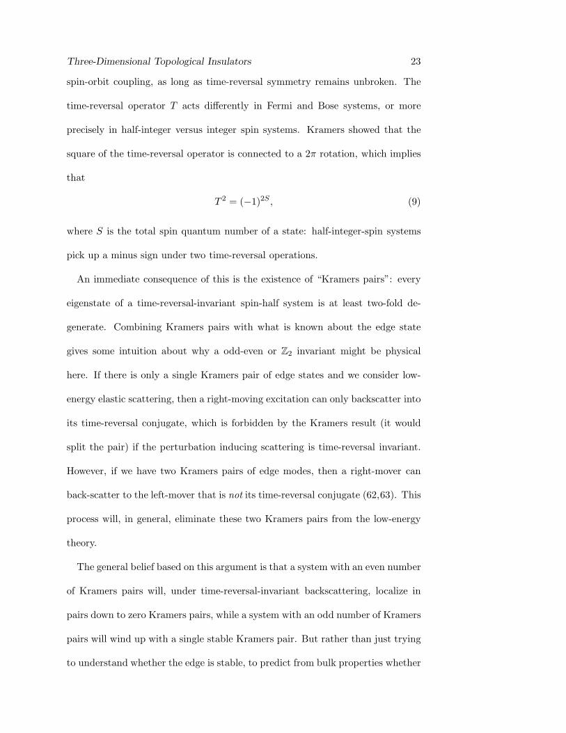
precisely in half-integer versus integer spin systems. Kramers showed that the
square of the time-reversal operator is connected to a 2π rotation, which implies
that
T 2 = (−1)2S , (9)
where S is the total spin quantum number of a state: half-integer-spin systems
pick up a minus sign under two time-reversal operations.
An immediate consequence of this is the existence of “Kramers pairs”: every
eigenstate of a time-reversal-invariant spin-half system is at least two-fold de-
generate. Combining Kramers pairs with what is known about the edge state
gives some intuition about why a odd-even or Z2 invariant might be physical
here. If there is only a single Kramers pair of edge states and we consider low-
energy elastic scattering, then a right-moving excitation can only backscatter into
its time-reversal conjugate, which is forbidden by the Kramers result (it would
split the pair) if the perturbation inducing scattering is time-reversal invariant.
However, if we have two Kramers pairs of edge modes, then a right-mover can
back-scatter to the left-mover that is not its time-reversal conjugate (62,63). This
process will, in general, eliminate these two Kramers pairs from the low-energy
theory.
The general belief based on this argument is that a system with an even number
of Kramers pairs will, under time-reversal-invariant backscattering, localize in
pairs down to zero Kramers pairs, while a system with an odd number of Kramers
pairs will wind up with a single stable Kramers pair. But rather than just trying
to understand whether the edge is stable, to predict from bulk properties whether
24 Hasan & Moore
the edge will have an even or odd number of Kramers pairs. Kane and Mele
showed that starting from the 2D T -invariant crystal, there are two topological
classes; instead of an integer-valued topological invariant, there is a “Z2 invariant
with two values, “even” and “odd”. Several formulations of this invariant are now
available (57, 64, 65, 66, 4). The even and odd classes correspond in the example
above (of separated up- and down-spins) to paired IQHE states with even or odd
Chern number for one spin.
We expect that, as for the IQHE, it should be possible to reinterpret the Z2
invariant as an invariant that describes the response of a finite toroidal system
to some perturbation. In the IQHE, the response is the amount of charge that is
pumped around one circle of the torus as a 2π flux (i.e., a flux hc/e) is pumped
adiabatically through the other circle. The pumping definition for the 2D topo-
logical insulator involves a π-flux; one can consider pumping of “Z2” (or Kramers
degeneracy) from one boundary to another of a large cylinder (66) (local insertion
of a π flux similarly induces a degeneracy (67)). Alternately, a precise restate-
ment of the Z2 invariant closes the process after π flux insertion so that what
is pumped is ordinary charge. (61, 68) These approaches directly generalize the
Z2 invariant to disordered single-electron systems; this and other 3D effects have
recently been studied (69). For the 3D topological insulator, we will later intro-
duce an alternative to pumping, the magnetoelectric polarizability, that defines
the phase in the presence of interactions.
3.2 3D topological insulators
We review quickly the band structure invariants that were used in the first def-
initions of the 3D topological insulator (4, 6, 14). Since the key emergent prop-

Three-Dimensional Topological Insulators 25
erties are somewhat difficult to perceive directly from the bulk band structure
invariants, we then use a different picture to explain the surface state (6) and
magnetoelectric polarizability (70,71,72).
We start by asking to what extent the two-dimensional integer quantum Hall
effect can be generalized to three dimensions. A generalization of the previously
mentioned homotopy argument of Avron, Seiler, and Simon (56) can be used to
show that there are three Chern numbers per band in three dimensions, associated
with the xy, yz, and xz planes of the Brillouin zone. A more physical way to
view this is that a three-dimensional integer quantum Hall system consists of a
single Chern number and a reciprocal lattice vector that describes the “stacking”
of integer quantum Hall layers (73). The edge of this three-dimensional IQHE is
quite interesting: it can form a two-dimensional chiral metal, as the chiral modes
from each IQHE (74) combine and point in the same direction. (75,76)
Now consider the Brillouin zone of a three-dimensional time-reversal-invariant
material. Our approach, following the derivation of the 3D topological invariants
in (4), builds on the two-dimensional case. In the case of inversion symmetry, a
useful trick (7, 2) allows the integrals in the following approach to be expressed
simply in terms of the parity eigenvalues at the time-reversal-invariant points.
This led to the understanding of the detailed surface state structure (6) that was
important the experimental observation of the phase (1).
Concentrating on a single band pair, there is a Z2 topological invariant de-
fined in the two-dimensional problem with time-reversal invariance. Taking the
Brillouin zone to be a torus, there are two inequivalent xy planes that are dis-
tinguished from others by the way time-reversal acts: the kz = 0 and kz = ±π/a
planes are taken to themselves by time-reversal (note that ±π/a are equivalent
26 Hasan & Moore
because of the periodic boundary conditions). These special planes are essentially
copies of the two-dimensional problem, and we can label them by Z2 invariants
z0 = ±1, z±1 = ±1, where +1 denotes “even Chern parity” or ordinary 2D insu-
lator and −1 denotes “odd Chern parity” or topological 2D insulator. Other xy
planes are not constrained by time-reversal and hence do not have to have a Z2
invariant.
The most interesting 3D topological insulator phase (the “strong topological
insulator”, in the language of (6)) results when the z0 and z±1 planes are in
different 2D classes. This can occur if, moving in the z direction between these
two planes, one has a series of 2D problems that interpolate between ordinary and
topological insulators by breaking time-reversal. We will concentrate on this type
of 3D topological insulator here. Another way to make a 3D topological insulator
is to stack 2D topological insulators, but considering the edge of such a system
shows that it will not be very stable: since two “odd” edges combine to make an
“even” edge, which is unstable in the presence of T -invariant backscattering, we
call such a stacked system a “weak topological insulator” (6). This edge state
can appear at crystalline dislocations (77).
Above we found two xy planes with two-dimensional Z2 invariants. By the same
logic, we could identify four other such invariants x0, x±1, y0, y±1. However, not
all six of these invariants are independent: some geometry shows that there are
two relations, reducing the number of independent invariants to four:
x0x±1 = y0y±1 = z0z±1. (10)
(Sketch of geometry: to establish the first equality above, consider evaluating
the Fu-Kane 2D formula on the four EBZs described by the four invariants
x0, x+1, y0, y+1. These define a torus, on whose interior the Chern two-form
Three-Dimensional Topological Insulators 27
F is well-defined. Arranging the four invariants so that all have the same orien-
tation, the A terms drop out, and the F integral vanishes as the torus can be
shrunk to a loop. In other words, for some gauge choice the difference x0 − x+1
is equal to y0 − y+1. ) We can take these four invariants in three dimensions
as (x0, y0, z0, x0x±1), where the first three describe layered “weak” topological
insulators, and the last describes the strong topological insulator (STI), which
is the one typically meant by ”3D topological insulator”. The “axion electrody-
namics” field theory in the next subsection is consistent with there being only
one genuinely three-dimensional Z2 invariant.
This derivation shows that the strong topological insulator cannot be realized
in any model with Sz conservation, while, as explained earlier, a useful example of
the 2D topological insulator (a.k.a. “quantum spin Hall effect”) can be obtained
from combining IQHE phases of up and down electrons. The impossibility of
making an STI with Sz conservation follows from noting that all planes normal
to z have the same Chern number, as Chern number is a topological invariant
whether or not the plane is preserved by time-reversal. In particular, the kz =
0 and kz = ±π/a phases have the same Chern number for up electrons, say,
which means that these two planes are either both 2D ordinary or 2D topological
insulators.
While the above argument is rather general, it does not give much insight into
what sort of gapless surface states we should expect at the surface of a strong
topological insulator. The spin-resolved surface Fermi surface encloses an odd
number of Dirac points (6). In the simplest case of a single Dirac point, believed
to be realized in Bi2Se3, the surface state can be pictured as “one-quarter of
graphene.” Graphene, a single layer of carbon atoms that form a honeycomb
28 Hasan & Moore
lattice, has two Dirac points and two spin states at each k; spin-orbit coupling
is quite weak since carbon is a relatively light element. The surface state of
a three-dimensional topological insulator can have a single Dirac point and a
single spin state at each k. As in the edge of the 2D topological insulator, time-
reversal invariance implies that the spin state at k must be the T conjugate of
the spin state at −k. This picture of the surface state can be obtained by work-
ing backward; in the following section we will effectively redefine a topological
insulator as a material whose surfaces, when gapped by a weak magnetic field,
have half-integer quantum hall effect, and since each Dirac fermion at the surface
contributes a half-integer when gapped, there must have been an odd number
prior to the magnetic perturbation.
4 TOPOLOGICAL INSULATORS AND ORBITAL MAGNE-
TOELECTRIC POLARIZABILITY
The three-dimensional topological insulator turns out to be connected to a basic
electromagnetic property of solids: the orbital contribution to the magnetoelectric
polarizability dP/dB (70,71,72). We know that in an insulating solid, Maxwell’s
equations can be modified because the dielectric constant ǫ and magnetic per-
meability µ need not take their vacuum values. Another effect is that solids can
generate the electromagnetic term
∆LEM =θe2
2πhE ·B =
θe2
16πhǫαβγδFαβFγδ . (11)
This term describes a magnetoelectric polarizability: an applied electrical field
generates a magnetic dipole, and vice versa. An essential feature of the above
“axion electrodynamics” (cf. Wilczek, 1987 (78) and references therein) is that,
Three-Dimensional Topological Insulators 29
when the axion field θ(x, t) is constant, it plays no role in electrodynamics; this
follows because θ couples to a total derivative, ǫαβγδFαβFγδ = 2ǫαβγδ∂α(AβFγδ)
(here we used that F is closed, i.e., dF = 0), and so does not modify the equa-
tions of motion. However, the presence of the axion field can have profound
consequences at surfaces and interfaces, where gradients in θ(x) appear.
A bit of work shows that, at a surface where θ changes, there is a surface
quantum Hall layer of magnitude
σxy =e2(∆θ)
2πh. (12)
(This can be obtained by moving the derivative from one of the A fields to act on
θ, leading to a Chern-Simons term for the EM field at the surface, which gives an
integer quantum Hall effect.) The magnetoelectric polarizability described above
can be obtained from these layers: for example, an applied electric field generates
circulating surface currents, which in turn generate a magnetic dipole moment.
In a sense, σxy is what accumulates at surfaces because of the magnetoelectric
polarizability, in the same way as charge is what accumulates at surfaces because
of ordinary polarization.
We write θ as an angle because, like polarization, θ is only well defined as a bulk
property modulo 2π. The integer multiple of 2π is only specified once we specify
a particular way to make the boundary. The connection to the 3D topological
insulator? (70) At first glance, θ = 0 in any time-reversal-invariant system, since
θ → −θ under time-reversal. However, since θ is periodic, θ = π also works, as
−θ and θ are equivalent because of the periodicity, and is inequivalent to θ = 0.
In a band structure of noninteracting electrons, θ receives a contribution from
30 Hasan & Moore
the integral of the Chern-Simons form:
θ = − 1
4π
∫
BZd3k ǫijk Tr[Ai∂jAk − i
2
3AiAjAk]. (13)
Qi, Hughes, and Zhang obtained this term by working down from the 4D quan-
tum Hall effect, as explained below. It can also be obtained (71) from semi-
classical results on polarization in inhomogeneous systems (79) or more direct
approaches (72, 80). The improvement is that these make clear that, for a gen-
eral solid (not necessarily a topological insulator), the Chern-Simons integral is
just one contribution to the electromagnetic θ. Here we sketch on understanding
the physical and mathematical meaning of the Chern-Simons form that consti-
tutes the integrand, chiefly by discussing analogies with our previous treatment of
polarization in one dimension and the IQHE in two dimensions. These analogies
and some important differences are summarized in Table I.
In this section,
Fij = ∂iAj − ∂jAi − i[Ai,Aj ] (14)
is the (generally non-Abelian) Berry curvature tensor (Aλ = i〈u|∂λ|u〉), and the
trace and commutator refer to band indices. We can understand the Chern-
Simons form K = Tr[Ai∂jAk − i23AiAjAk] that appears in the integral above
starting from the second Chern form Tr[F ∧F ]; the relationship between the two
is that
dK = Tr[F ∧ F ], (15)
just as A is related to the first Chern form: d(TrA) = TrF . These relationships
hold locally (this is known as Poincare’s lemma, that any closed form is locally an
exact form) but not globally, unless the first or second Chern form is trivial (i.e.,
generates the trivial cohomology class. For example, the existence of a nonzero

Three-Dimensional Topological Insulators 31
first Chern number on the sphere prevents us from finding globally defined wave-
functions that would give an A with dA = F . We are assuming in even writing
the Chern-Simons formula for θ that the ordinary Chern numbers are zero, so
that an A can be defined in the 3D Brillouin zone. We would run into trouble
if we assumed that an A could be defined in the 4D Brillouin zone if the first or
second Chern number were nonzero. The second Chern number invariant of a 4D
band structure (53) underlies the four-dimensional quantum Hall effect (54).
Although this 4D QHE is not directly measurable, it is mathematically con-
nected to the 3D magnetoelectric polarizability in the same way as 1D polariza-
tion and the 2D IQHE are connected. But a difference is that the Berry phase
entirely determines 1D polarization, while in general the orbital magnetoelectric
polarizability of a 3D crystal, even its diagonal part, contains further terms be-
yond the Berry phase (the correct expression is in (72,80)). But these “ordinary”
terms disappear in either the “topological” limit of (70) where all occupied bands
have the same energy -1 and all unoccupied bands have the same energy +1, or in
topological insulators, where the only surviving term is (Eq. 13). Hence in many
simple models in the literature the extra terms actually vanish; an exception is a
pyrochlore lattice model (81).
We can give a many-body understanding of θ that clarifies the geometric rea-
son for its periodicity even in a many-particle system (71). Consider evaluating
dP/dB by applying the 3D formula
Pi = e
∫
BZ
d3k
(2π)3TrAi . (16)
which generalizes to interacting systems (82) via the flux trick, to a rectangular-
prism unit cell. The minimum magnetic field normal to one of the faces that can
be applied to the cell without destroying the periodicity is one flux quantum per
32 Hasan & Moore
unit cell (83), or a field strength h/(eΩ), where Ω is the area of that face. The
ambiguity of polarization (16) in this direction is one charge per transverse unit
cell area, i.e., e/Ω. Then the ambiguity in dP/dB is, choosing the x direction,
∆Px
Bx=
e/Ω
h/(eΩ)=e2
h= 2π
e2
2πh. (17)
So the periodicity of 2π in θ is a consequence of the geometry of polarization, and
is independent of the single-electron assumption that leads to the microscopic
Chern-Simons formula. The surface interpretation of the periodicity is that it
results from the freedom to add a surface integer quantum Hall layer without
any change in the bulk properties. (Adding a fractional quantum Hall layer
involves additional subtleties related to the topological ground state degeneracy.)
5 RECENT DEVELOPMENTS: STRONG CORRELATIONS
AND MAJORANA FERMIONS
Many of the topics of greatest recent interest, both theoretically and experimen-
tally, involve connections between strongly correlated electrons and topological
insulators. There could be materials in which the topological insulator behavior
emerges as a result of electron correlations (a 2D theoretical model is introduced
in (84)). Similar behavior to that in simple topological insulators can occur
in Kondo lattice systems (85)) and in antiferromagnets (86). In Mott insula-
tors, emergent fermionic excitations (spinons) could form a topological phase
with surfaces that are electrically insulating but thermally conducting (87). In-
teractions could lead to spontaneous instabilities at the surfaces of topological
insulators (88).
It seems fitting to end our review by explaining how topological insulators
Three-Dimensional Topological Insulators 33
might enable creation and observation of one of the most long-sought particles of
nature. A Majorana fermion is a fermion that is its own antiparticle, unlike an
ordinary (Dirac) fermion such as the electron, which has a distinct antiparticle
(positron or hole). The search for Majorana fermions as fundamental particles
continues, but it is now believed that several condensed matter systems may
support emergent Majorana fermion excitations, and possible observation of a
Majorana fermion was reported in 2009 by Willett et al. (89) by interferometric
transport on the ν = 5/2 fractional quantum Hall state.
Majorana fermions can be created in several ways using topological insulators.
The most direct proposal using a 3D topological insulator is to consider the prox-
imity effect from an ordinary s-wave superconductor. The result (90) (Figure 9)
is an interface layer of 2D “topological superconductor” that is distinct but sim-
ilar to the 2D p+ ip superconductor that has been understood for some time to
support Majorana fermions. A magnetic vortex core in such a system will carry
a zero-energy Majorana fermion state localized near the vortex in the interface
layer, as well as possibly ordinary electronic modes.
There have been many recent works discussing either how the Majorana mode
could be detected (using, e.g., noise (91), interferometry (92,93)) and on collective
behavior of Majoranas, e.g., in a random system of vortices (94) or an array (95)).
There are analogous ways to create a Majorana fermion using strong spin-orbit
quantum wells rather than topological insulators (96, 97, 98). These ideas for
probes may also be helpful in understanding whether CuxBi2Se3 (39, 99) is a
topological superconductor.
We have tried to convey that, only two years after the first experimental paper
on topological insulators, work in this field is proceeding on many fronts. Our

34 Hasan & Moore
basic ideas of such established concepts as spin-orbit coupling and band struc-
ture have already had to be rethought, and there are good reasons to anticipate
further advances in our understanding. The authors have enjoyed too many col-
laborations and discussions in this field to acknowledge all by name; they are
especially grateful to their colleagues for creating stimulating academic environ-
ments at Princeton (MZH) and Berkeley (JEM). Funding was provided by DOE
and NSF (MZH) and by NSF DMR-0804413 and WIN (JEM).
Literature Cited
1. Hsieh D, Qian D, Wray L, Xia Y, Hor YS, et al., Nature 452:970 (2008).
2. Hasan MZ, Kane CL, Rev. Mod. Phys. 82:3045 (2010).
3. Moore JE, Nature 464:194 (2010).
4. Moore JE, Balents L, Phys. Rev. B 75:121306(R) (2007).
5. Kane CL, Mele EJ, Phys. Rev. Lett. 95:146802 (2005).
6. Fu L, Kane CL, Mele EJ, Phys. Rev. Lett. 98:106803 (2007).
7. Fu L, Kane CL, Phys. Rev. B 76:045302 (2007).
8. Bernevig BA, Hughes TL, Zhang SC, Science 314:1757 (2006).
9. Koenig M, Wiedmann S, Bruene C, Roth A, Buhmann H, et al., Science
318:766 (2007).
10. Qi XL, Zhang SC, Physics Today 63:33 (2010).
11. Konig M, Buhmann H, Molenkamp LW, Hughes T, Liu C, et al., Journal of
the Physical Society of Japan 77:031007 (2008), 0801.0901.
12. Schnyder A, Ryu S, Furusaki A, Ludwig AWW, Phys. Rev. B 78:195125
(2008).
13. Kitaev A, Periodic table for topological insulators and superconductors,
Three-Dimensional Topological Insulators 35
arXiv:0901.0686, 2009.
14. Roy R, Phys. Rev. B 79:195322 (2009).
15. Teo JCY, Fu L, Kane C, Phys. Rev. B 78:045426 (2008).
16. Lenoir B, et al., in Fifteenth International Conference on Thermoelectrics
(Pasadena, California) 113 (IEEE, New York), 1996.
17. Liu Y, Allen E, Phys. Rev. B 52:1566 (1995).
18. Wolff PAJ, Phys. Chem. Solids 25:1057 (1964).
19. Hsieh D, et al., Science 323:919 (2009).
20. Roushan P, et al., Nature 460:1106 (2009).
21. Xia Y, et al., Nature Phys. 5:398 (2009).
22. Xia Y, et al., arXiv:0812.2078v1, 2008.
23. Hsieh D, et al., Nature 460:1101 (2009).
24. Anderson PW, Phys. Rev. 109:1492 (1958).
25. Zhang T, et al., Phys. Rev. Lett. 103:266803 (2009).
26. Alpichshev Z, et al., Physical Review Letters 104:016401 (2010).
27. Zhang H, et al., Nature Physics 5:438 (2009).
28. Noh HJ, et al., Europhys. Lett. 81:57006 (2008).
29. Hor YS, et al., Phys. Rev. B 79:195208 (2009).
30. Park SR, et al., Phys. Rev. B 81:041405 (2010).
31. Chen YL, et al., Science 325:178 (2009).
32. Hsieh D, et al., Phys. Rev. Lett. 103:146401 (2009).
33. Xia Y, et al., arXiv:0907.3089, 2009.
34. Moore J, Nature Physics 5:378 (2009).
35. Lin, et al., Nature Materials 9:546 (2010).
36. Fu L, Phys. Rev. Lett. 103:266801 (2009).
36 Hasan & Moore
37. Hasan MZ, Lin H, Bansil A, Physics 2:108 (2009).
38. Wray L, et al., unpublished, 2010.
39. Hor YS, et al., Phys. Rev. Lett. 104:057001 (2010).
40. Wray L, et al., arXiv:0912.3341v1, 2009.
41. Chadov, et al., Nature Materials 9:541 (2010).
42. Li YY, et al., Growth dynamics and thickness-dependent electronic structure
of topological insulator Bi2Te3 thin film on Si, arXiv:0912.5054, 2009.
43. Peng H, Lai K, Kong D, Meister S, Chen Y, et al., Nat. Mat. 9:225 (2010).
44. Bardarson JH, Brouwer PW, Moore JE, Aharonov-bohm oscillations in dis-
ordered topological insulator nanowires, arXiv:1005.3762, 2010.
45. Zhang Y, Vishwanath A, Anomalous aharonov-bohm conductance oscilla-
tions from topological insulator surface states, arXiv:1005.3542, 2010.
46. Lu HZ, et al., Phys. Rev. B 37:115407 (2010).
47. Seradjeh B, Moore JE, Franz M, Phys. Rev. Lett. 103:066402 (2009).
48. Thouless DJ, Kohmoto M, Nightingale MP, den Nijs M, Phys. Rev. Lett.
49:405 (1982).
49. Berry MV, Proc. Roy. Soc. A 392:45 (1984).
50. King-Smith RD, Vanderbilt D, Phys. Rev. B 47:1651 (1993).
51. Nakahara M, Geometry, Topology and Physics (Institute of Physics, 1998).
52. Resta R, Ferroelectrics 136:51 (1992).
53. Avron JE, Sadun L, Segert J, Simon B, Phys. Rev. Lett. 61:1329 (1988).
54. Zhang SC, Hu J, Science 294:823 (2001).
55. Niu Q, Thouless DJ, Wu YS, Phys. Rev. B 31:3372 (1985).
56. Avron JE, Seiler R, Simon B, Phys. Rev. Lett. 51:51 (1983).
57. Kane CL, Mele EJ, Phys. Rev. Lett. 95:226801 (2005).
Three-Dimensional Topological Insulators 37
58. Murakami S, Nagaosa N, Zhang SC, Phys. Rev. Lett. 93:156804 (2004).
59. Kane CL, Mele EJ, Phys. Rev. Lett. 95:146802 (2005).
60. Haldane FDM, Physical Review Letters 61:2015 (1988).
61. Essin AM, Moore JE, Phys. Rev. B 76:165307 (2007).
62. Xu C, Moore JE, Phys. Rev. B 73:045322 (2006).
63. Wu C, Bernevig BA, Zhang SC, Phys. Rev. Lett. 96:106401 (2006).
64. Bernevig BA, Zhang SC, Phys. Rev. Lett. 96:106802 (2006).
65. Roy R, Phys. Rev. B 79:195321 (2009).
66. Fu L, Kane CL, Phys. Rev. B 74:195312 (2006).
67. Ran Y, Vishwanath A, Lee DH, Phys. Rev. Lett. 101:086801 (2008).
68. Qi XL, Zhang SC, Phys. Rev. Lett. 101:086802 (2008).
69. Shindou R, Murakami S, Phys. Rev. B 79:045321 (2009).
70. Qi XL, Hughes TL, Zhang SC, Physical Review B 78:195424 (2008).
71. Essin AM, Moore JE, Vanderbilt D, Physical Review Letters 102:146805
(2009).
72. Essin AM, Turner AM, Moore JE, Vanderbilt D, Physical Review B
81:205104 (2010).
73. Halperin BI, Jpn. J. Appl. Phys. Suppl. 26:1913 (1987).
74. Halperin BI, Phys. Rev. B 25:2185 (1982).
75. Chalker JT, Dohmen A, Phys. Rev. Lett. 75:4496 (1995).
76. Balents L, Fisher MPA, Phys. Rev. Lett. 76:2782 (1996).
77. Ran Y, Zhang Y, Vishwanath A, Nature Phys. 5:298 (2009).
78. Wilczek F, Phys. Rev. Lett. 58:1799 (1987).
79. Xiao D, Shi J, Clougherty DP, Niu Q, Phys. Rev. Lett. 102:087602 (2009).
80. Malashevich A, Souza I, Coh S, Vanderbilt D, New Journal of Physics
38 Hasan & Moore
12:053032 (2010).
81. Guo HM, Franz M, Physical Review Letters 103:206805 (2009).
82. Ortiz G, Martin RM, Phys. Rev. B 49:14202 (1994).
83. Zak J, Phys. Rev. 134:A1602 (1964).
84. Raghu S, Qi XL, Honerkamp C, Zhang SC, Phys. Rev. Lett. 100:156401
(2008).
85. Dzero M, Sun K, Galitski V, Coleman P, Phys. Rev. Lett. 104:106408 (2010).
86. Mong R, Essin AM, Moore JE, Phys. Rev. B 81:245209 (2010).
87. Pesin DA, Balents L, Nature Physics 6:376 (2010).
88. Xu C, Phys. Rev. B 81:054403 (2010).
89. Willett RL, Pfeiffer LN, West KW, PNAS 106:8853 (2009).
90. Fu L, Kane CL, Phys. Rev. Lett. 100:096407 (2008).
91. Nilsson J, Akhmerov AR, Beenakker CW, Phys. Rev. Lett. 101:120403
(2008).
92. Akhmerov AR, Nilsson J, Beenakker CWJ, Phys. Rev. Lett. 102:216404
(2009).
93. Fu L, Kane CL, Phys. Rev. Lett. 102:216403 (2009).
94. Shivamoggi V, Refael G, Moore JE, Majorana fermion chain at the quantum
spin hall edge, arXiv:1004.4585, 2010.
95. Xu C, Fu L, Phys. Rev. B 81:134435 (2010).
96. Sato M, Fujimoto S, Phys. Rev. B 79:094504 (2009).
97. Sau JD, Lutchyn RM, Tewari S, Sarma SD, Phys. Rev. Lett. 104:040502
(2010).
98. Alicea J, Phys. Rev. B 81:125318 (2010).
99. Fu L, Berg E, arXiv:0912.3294, 2010.
Three-Dimensional Topological Insulators 39
List of Figures
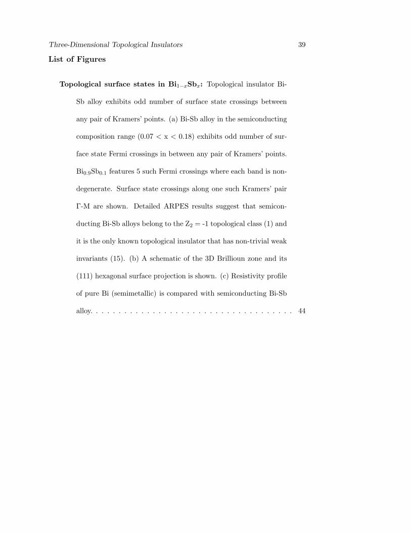
Topological surface states in Bi1−xSbx: Topological insulator Bi-
Sb alloy exhibits odd number of surface state crossings between
any pair of Kramers’ points. (a) Bi-Sb alloy in the semiconducting
composition range (0.07 < x < 0.18) exhibits odd number of sur-
face state Fermi crossings in between any pair of Kramers’ points.
Bi0.9Sb0.1 features 5 such Fermi crossings where each band is non-
degenerate. Surface state crossings along one such Kramers’ pair
Γ-M are shown. Detailed ARPES results suggest that semicon-
ducting Bi-Sb alloys belong to the Z2 = -1 topological class (1) and
it is the only known topological insulator that has non-trivial weak
invariants (15). (b) A schematic of the 3D Brillioun zone and its
(111) hexagonal surface projection is shown. (c) Resistivity profile
of pure Bi (semimetallic) is compared with semiconducting Bi-Sb
alloy. . . . . . . . . . . . . . . . . . . . . . . . . . . . . . . . . . . . 44
40 Hasan & Moore
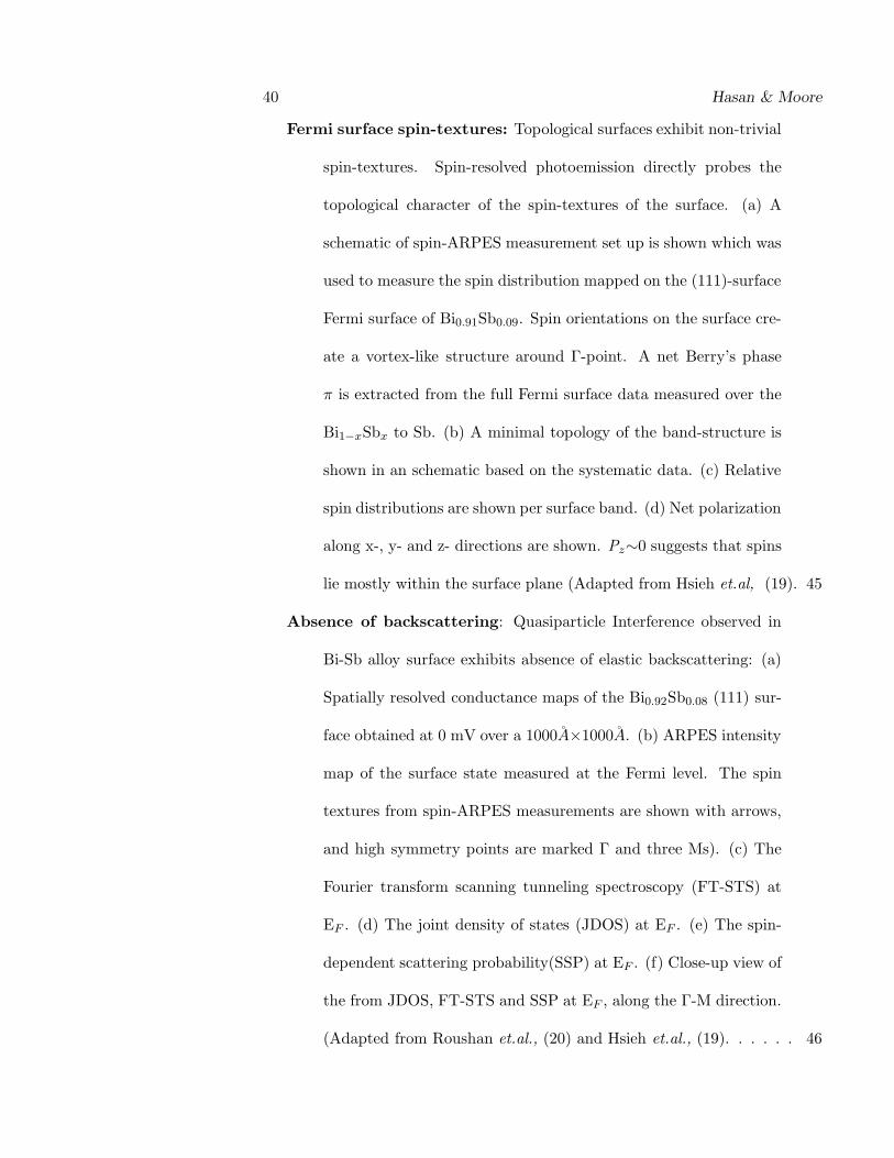
Fermi surface spin-textures: Topological surfaces exhibit non-trivial
spin-textures. Spin-resolved photoemission directly probes the
topological character of the spin-textures of the surface. (a) A
schematic of spin-ARPES measurement set up is shown which was
used to measure the spin distribution mapped on the (111)-surface
Fermi surface of Bi0.91Sb0.09. Spin orientations on the surface cre-
ate a vortex-like structure around Γ-point. A net Berry’s phase
π is extracted from the full Fermi surface data measured over the
Bi1−xSbx to Sb. (b) A minimal topology of the band-structure is
shown in an schematic based on the systematic data. (c) Relative
spin distributions are shown per surface band. (d) Net polarization
along x-, y- and z- directions are shown. Pz∼0 suggests that spins
lie mostly within the surface plane (Adapted from Hsieh et.al, (19). 45
Absence of backscattering: Quasiparticle Interference observed in
Bi-Sb alloy surface exhibits absence of elastic backscattering: (a)
Spatially resolved conductance maps of the Bi0.92Sb0.08 (111) sur-
face obtained at 0 mV over a 1000A×1000A. (b) ARPES intensity
map of the surface state measured at the Fermi level. The spin
textures from spin-ARPES measurements are shown with arrows,
and high symmetry points are marked Γ and three Ms). (c) The
Fourier transform scanning tunneling spectroscopy (FT-STS) at
EF . (d) The joint density of states (JDOS) at EF . (e) The spin-
dependent scattering probability(SSP) at EF . (f) Close-up view of
the from JDOS, FT-STS and SSP at EF , along the Γ-M direction.
(Adapted from Roushan et.al., (20) and Hsieh et.al., (19). . . . . . 46

Three-Dimensional Topological Insulators 41
Single Dirac cone fermions: Spin-momentum locked helical surface
Dirac fermions are hallmark signatures of bulk topological Z2 or-
der. The single-Dirac-cone per surface topological insulators be-
long to the (νo=1,000) topological class. (a) Surface dispersion
relation of electronic states reveal a spin-polarized Dirac cone.
(b) Surface Fermi surface exhibits chiral left-handed spin textures.
Schematic presentations of (c) surface and bulk band topology and
(d) a single spin-polarized Dirac fermion on the surface of Bi2X3
(νo=1,000) topological insulators. (e) Constant-energy deposition
maps of the surface state are labeled with spin texture. (Adapted
from Xia et.al., (21,22); Hsieh et.al., (23)) . . . . . . . . . . . . . . 47
Surface Dirac points are protected by time reversal symme-
try: (a) The surface state dispersion is compared before and after
deposition, using hollow circles to indicate data and lines to trace
ideal Dirac dispersions. After deposition, the upper Dirac cone
gains a mass of 0.1 electron masses. (b) The evolution of Bi2Se3
surface states as a function of surface Fe deposition is shown for
a p-type Bi2Se3 sample hole doped with 0.25% Ca. (c, left) A z-
axis magnetic perturbation causes (green) GGA predicted surface
states to conform to the iron doped dispersion. (right) A surface
insulator phase can likely be obtained by adding a non-magnetic
p-type surface dopant such as NO2 subsequent to Fe deposition.
(d) A cartoon illustrates the charge and magnetic perturbations
caused by Fe deposition on the TI surface. . . . . . . . . . . . . . . 48
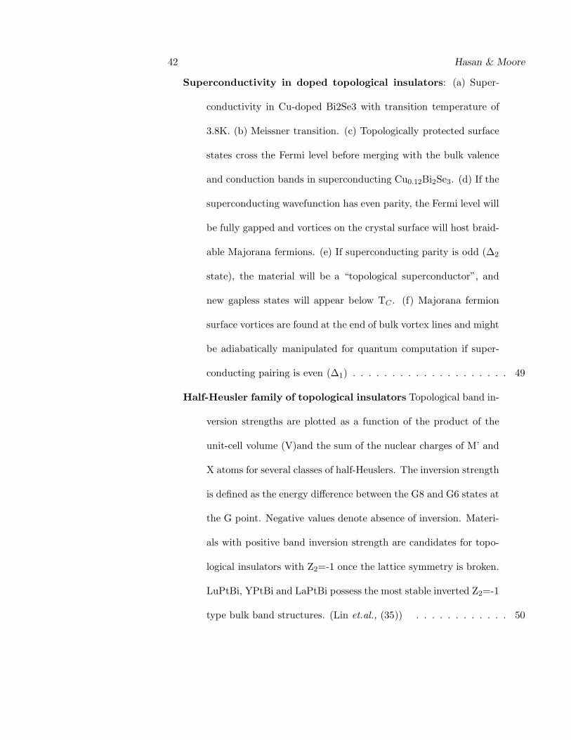
42 Hasan & Moore
Superconductivity in doped topological insulators: (a) Super-
conductivity in Cu-doped Bi2Se3 with transition temperature of
3.8K. (b) Meissner transition. (c) Topologically protected surface
states cross the Fermi level before merging with the bulk valence
and conduction bands in superconducting Cu0.12Bi2Se3. (d) If the
superconducting wavefunction has even parity, the Fermi level will
be fully gapped and vortices on the crystal surface will host braid-
able Majorana fermions. (e) If superconducting parity is odd (∆2
state), the material will be a “topological superconductor”, and
new gapless states will appear below TC . (f) Majorana fermion
surface vortices are found at the end of bulk vortex lines and might
be adiabatically manipulated for quantum computation if super-
conducting pairing is even (∆1) . . . . . . . . . . . . . . . . . . . . 49
Half-Heusler family of topological insulators Topological band in-
version strengths are plotted as a function of the product of the
unit-cell volume (V)and the sum of the nuclear charges of M’ and
X atoms for several classes of half-Heuslers. The inversion strength
is defined as the energy difference between the G8 and G6 states at
the G point. Negative values denote absence of inversion. Materi-
als with positive band inversion strength are candidates for topo-
logical insulators with Z2=-1 once the lattice symmetry is broken.
LuPtBi, YPtBi and LaPtBi possess the most stable inverted Z2=-1
type bulk band structures. (Lin et.al., (35)) . . . . . . . . . . . . 50
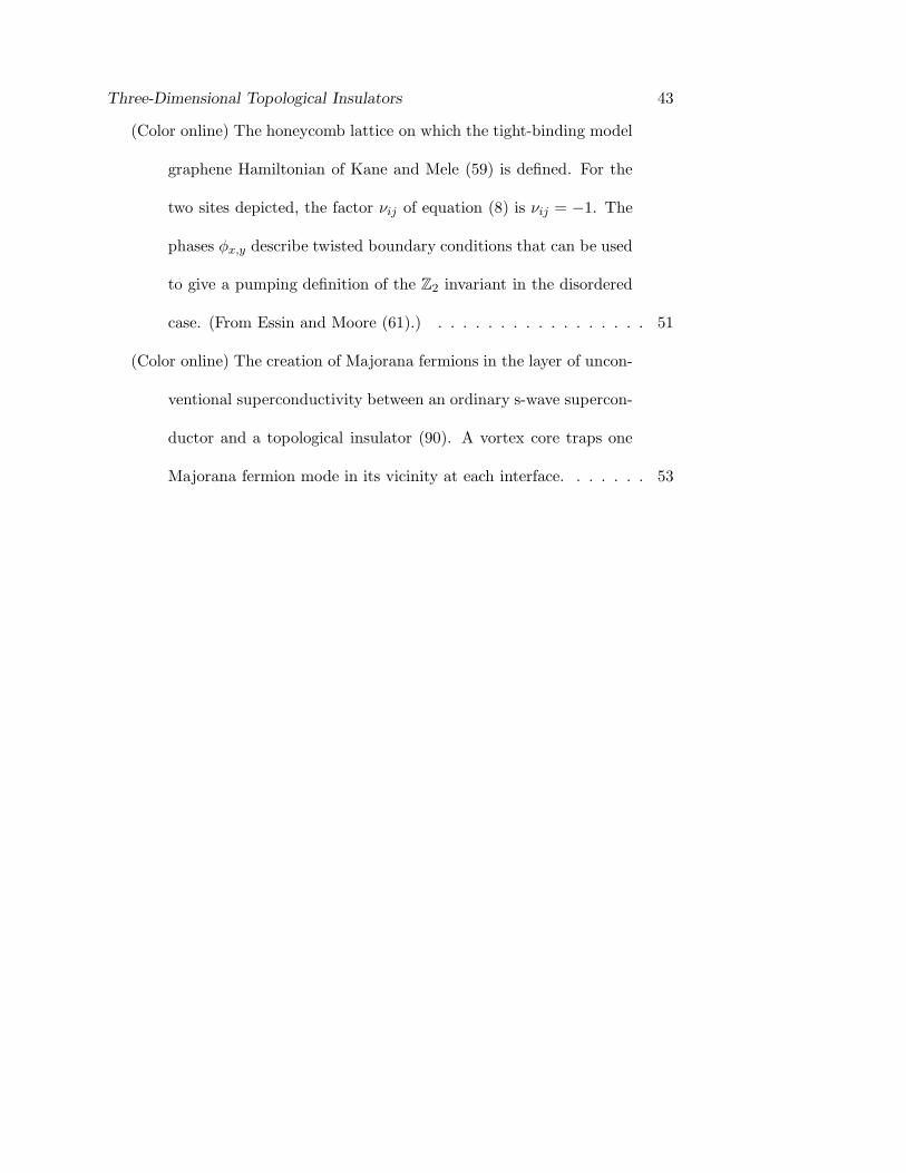
Three-Dimensional Topological Insulators 43
(Color online) The honeycomb lattice on which the tight-binding model
graphene Hamiltonian of Kane and Mele (59) is defined. For the
two sites depicted, the factor νij of equation (8) is νij = −1. The
phases φx,y describe twisted boundary conditions that can be used
to give a pumping definition of the Z2 invariant in the disordered
case. (From Essin and Moore (61).) . . . . . . . . . . . . . . . . . 51
(Color online) The creation of Majorana fermions in the layer of uncon-
ventional superconductivity between an ordinary s-wave supercon-
ductor and a topological insulator (90). A vortex core traps one
Majorana fermion mode in its vicinity at each interface. . . . . . . 53
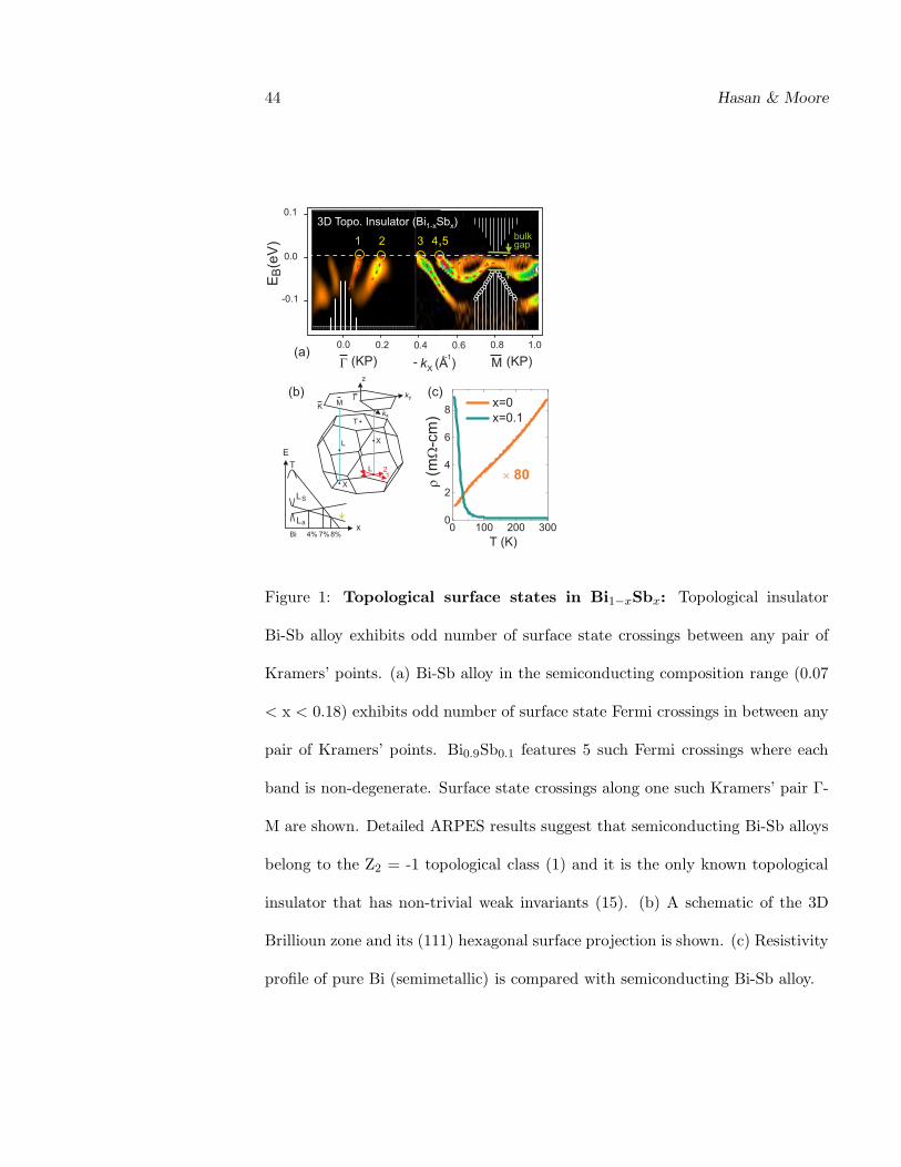
44 Hasan & Moore
0 100 200 3000
2
4
6
8
´ 80
r(m
W-c
m)
T (K)
x=0x=0.1
1 2
0.0 0.2 0.4 0.6 0.8 1.0
G Mk (Å )X
-1
0.0
-0.1
E
(eV
)B
0.1
3 4 5,
-(KP) (KP)
bulkgap
(a)
3D Topo. Insulator (Bi Sb1-x x)
(c)
T
KG
k
z
1
L
2L
X
x
M
X
ky
E
x
T
L
L
S
a
4% 7% 8%Bi
(b)
Figure 1: Topological surface states in Bi1−xSbx: Topological insulator
Bi-Sb alloy exhibits odd number of surface state crossings between any pair of
Kramers’ points. (a) Bi-Sb alloy in the semiconducting composition range (0.07
< x < 0.18) exhibits odd number of surface state Fermi crossings in between any
pair of Kramers’ points. Bi0.9Sb0.1 features 5 such Fermi crossings where each
band is non-degenerate. Surface state crossings along one such Kramers’ pair Γ-
M are shown. Detailed ARPES results suggest that semiconducting Bi-Sb alloys
belong to the Z2 = -1 topological class (1) and it is the only known topological
insulator that has non-trivial weak invariants (15). (b) A schematic of the 3D
Brillioun zone and its (111) hexagonal surface projection is shown. (c) Resistivity
profile of pure Bi (semimetallic) is compared with semiconducting Bi-Sb alloy.
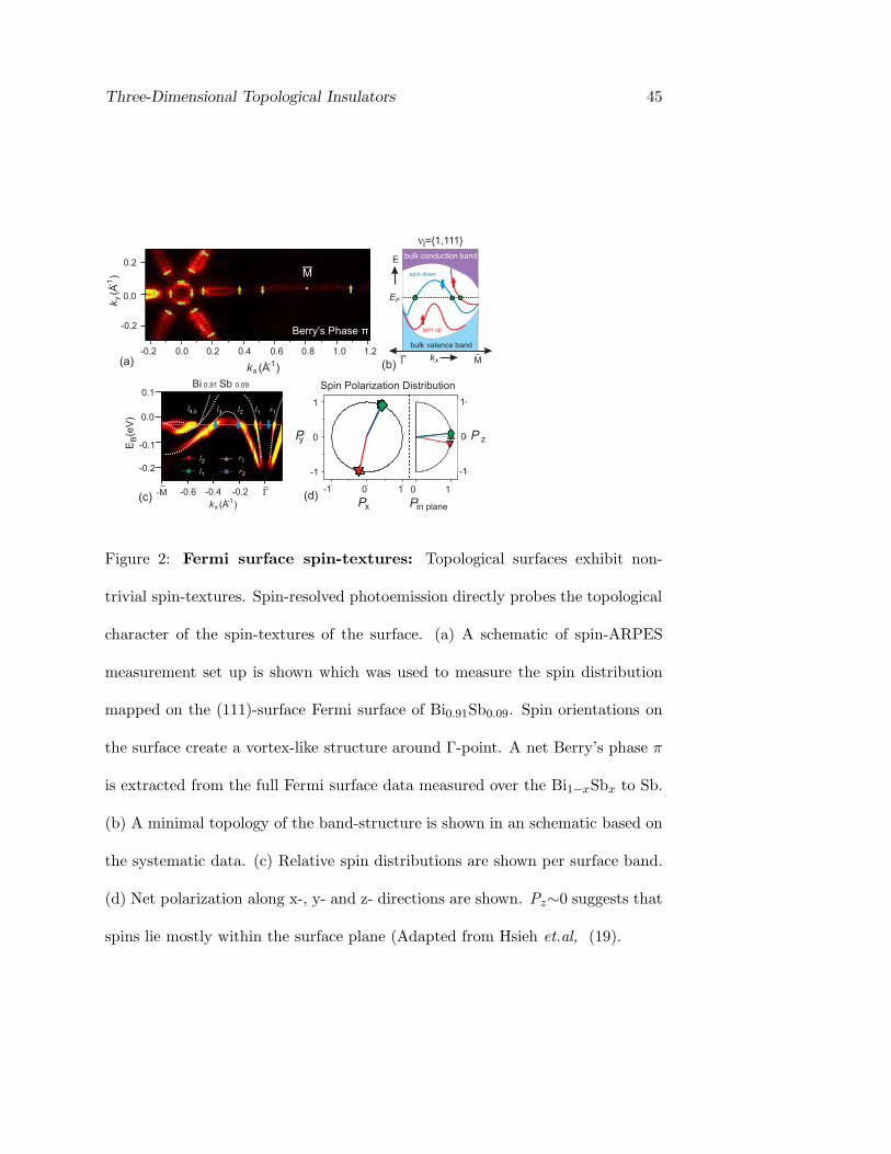
Three-Dimensional Topological Insulators 45
-0.2
-0.1
0.0
0.1
-0.2
0.0
0.2
Deg
1.21.00.80.60.40.20.0-0.2-0.2 0.0 0.2 0.4 0.6
-0.2
0.0
0.2
k (Å )x-1
0.8 1.0 1.2
M
k(Å
)
y-1
Berry’s Phase π
EF
E bulk conduction band
bulk valence band
spin down
spin up
0.0
-0.1
-0.2
0.1
r1l2l3l4,5
G-0.2-0.4-0.6-Mk (Å )x
-1
l1
Bi Sb0.91 0.09
E
(eV
)B
l2
l1
r1
r2
-1 0 1
-1
0
1
0.0 1.0
-1.0
0.0
1.0
0-1 1 0 1
-1
0
1
-1
0
1
Px
Py P z
Pin plane
G Mkx(a) (b)
(c) (d)
Spin Polarization Distribution
νi=1,111
Figure 2: Fermi surface spin-textures: Topological surfaces exhibit non-
trivial spin-textures. Spin-resolved photoemission directly probes the topological
character of the spin-textures of the surface. (a) A schematic of spin-ARPES
measurement set up is shown which was used to measure the spin distribution
mapped on the (111)-surface Fermi surface of Bi0.91Sb0.09. Spin orientations on
the surface create a vortex-like structure around Γ-point. A net Berry’s phase π
is extracted from the full Fermi surface data measured over the Bi1−xSbx to Sb.
(b) A minimal topology of the band-structure is shown in an schematic based on
the systematic data. (c) Relative spin distributions are shown per surface band.
(d) Net polarization along x-, y- and z- directions are shown. Pz∼0 suggests that
spins lie mostly within the surface plane (Adapted from Hsieh et.al, (19).
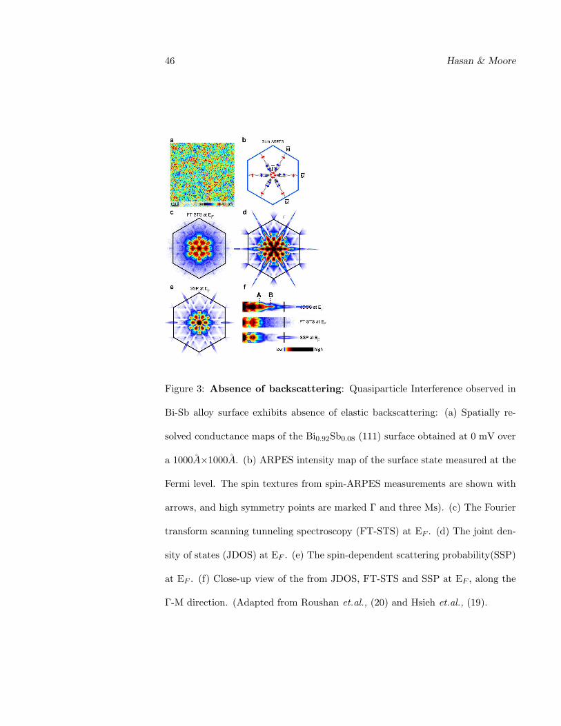
46 Hasan & Moore
Figure 3: Absence of backscattering: Quasiparticle Interference observed in
Bi-Sb alloy surface exhibits absence of elastic backscattering: (a) Spatially re-
solved conductance maps of the Bi0.92Sb0.08 (111) surface obtained at 0 mV over
a 1000A×1000A. (b) ARPES intensity map of the surface state measured at the
Fermi level. The spin textures from spin-ARPES measurements are shown with
arrows, and high symmetry points are marked Γ and three Ms). (c) The Fourier
transform scanning tunneling spectroscopy (FT-STS) at EF . (d) The joint den-
sity of states (JDOS) at EF . (e) The spin-dependent scattering probability(SSP)
at EF . (f) Close-up view of the from JDOS, FT-STS and SSP at EF , along the
Γ-M direction. (Adapted from Roushan et.al., (20) and Hsieh et.al., (19).
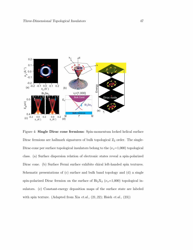
Three-Dimensional Topological Insulators 47
x
Dirac node
(e)
-0.2
-0.1
0.0
0.1
0.2
-0.2 -0.1 0.0 0.1 0.2
k
ky
ky
(Å)
-1
kx (Å )-1(a) (b)
E
kx (Å )-1 ky (Å )-1
ΓM M K
E (e
V)
B
ΓM M
Bi Se2 3
EF
Bulk Cond.
Bulk Valence
Bi Se2 3
(c) (d)
νi=1,000KΓ
Energ
y
k ykx
-0.2 0.0 0.2 0.0 0.20.4
0.0
Figure 4: Single Dirac cone fermions: Spin-momentum locked helical surface
Dirac fermions are hallmark signatures of bulk topological Z2 order. The single-
Dirac-cone per surface topological insulators belong to the (νo=1,000) topological
class. (a) Surface dispersion relation of electronic states reveal a spin-polarized
Dirac cone. (b) Surface Fermi surface exhibits chiral left-handed spin textures.
Schematic presentations of (c) surface and bulk band topology and (d) a single
spin-polarized Dirac fermion on the surface of Bi2X3 (νo=1,000) topological in-
sulators. (e) Constant-energy deposition maps of the surface state are labeled
with spin texture. (Adapted from Xia et.al., (21,22); Hsieh et.al., (23))

48 Hasan & Moore
Fe DopedM=0.1MeUndopedM=0
a
0
.1
.2
0.1-0.1 0
En
erg
y (e
V)
Momentum ( -1)Å
.3
0.5
eV
0-0.1 0.1
+Fe
-.1 .10
D2
-.1 .10 -.1 .10
D1
-.1 .10-.1 .10
D0
.4
.8
0
Bin
d. E
nerg
y (e
V)
b
12minFe deposition time3min
Sample #1
Bin
d. E
nerg
y (e
V)
0-.1 .1
.4
.8
c
Momentum kx ( -1)Å
0
d
+
++
+ +
+ ++
0-.1 .1
Theory
Perturbed TISurface
Δ4L
NO
2
EFΔ
Figure 5: Surface Dirac points are protected by time reversal symmetry:
(a) The surface state dispersion is compared before and after deposition, using
hollow circles to indicate data and lines to trace ideal Dirac dispersions. After
deposition, the upper Dirac cone gains a mass of 0.1 electron masses. (b) The
evolution of Bi2Se3 surface states as a function of surface Fe deposition is shown
for a p-type Bi2Se3 sample hole doped with 0.25% Ca. (c, left) A z-axis magnetic
perturbation causes (green) GGA predicted surface states to conform to the iron
doped dispersion. (right) A surface insulator phase can likely be obtained by
adding a non-magnetic p-type surface dopant such as NO2 subsequent to Fe
deposition. (d) A cartoon illustrates the charge and magnetic perturbations
caused by Fe deposition on the TI surface.
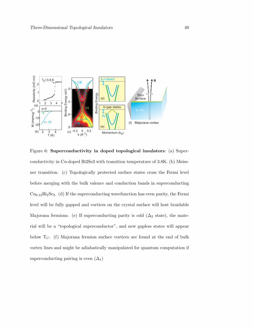
Three-Dimensional Topological Insulators 49
VB
SS
Bin
din
g E
nerg
y
in-gap states
Δ2Bin
din
g E
nerg
y (e
V)
(c)
0
.3
.6
.9
Δ1=.6meVCB
k (Å-1)0 0.2-0.2
(d)
(e)
Momentum (kx)
Majorana vortex
Δ1 SC
TopoSurface
(f)
B
3 4 5
Tc=3.8 K
2
.1
0
.2
Resi
stiv
ity (
mcm
)Ω
(a)1
0
-10
-20M (
mem
ug
-1)
2 3 4
x=0
.1
x=.12
T (K)(b)
Figure 6: Superconductivity in doped topological insulators: (a) Super-
conductivity in Cu-doped Bi2Se3 with transition temperature of 3.8K. (b) Meiss-
ner transition. (c) Topologically protected surface states cross the Fermi level
before merging with the bulk valence and conduction bands in superconducting
Cu0.12Bi2Se3. (d) If the superconducting wavefunction has even parity, the Fermi
level will be fully gapped and vortices on the crystal surface will host braidable
Majorana fermions. (e) If superconducting parity is odd (∆2 state), the mate-
rial will be a “topological superconductor”, and new gapless states will appear
below TC . (f) Majorana fermion surface vortices are found at the end of bulk
vortex lines and might be adiabatically manipulated for quantum computation if
superconducting pairing is even (∆1)

50 Hasan & Moore
2
1.5
1
0.5
0
0.5
1
1.5
2
2.5
15 25 35 45 55
Pb
Sb
Sn
Bi
Z2= 1
ScNiBi
YNiBi
LuNiBiScPdBi
LuPdBi
YPdBi
LaPtBi
YPtBi
LuPtBi
YAuPb
ScPdSb
YPdSb
ScPtSb
YPtSb
ScAuSn
LuPtSb
LuAuSn
LaPdBi
Ban
d!In
vers
ion!S
tren
gth
![eV
]
15 25 35 45 55
(ZM +ZX)!*V![nm3]
2.5
2.0
1.5
1.0
0.5
0.0
-0.5
-1.0
-1.5
-2.0
Topological half-Heusler family
Z2=+1
Figure 7: Half-Heusler family of topological insulators Topological band
inversion strengths are plotted as a function of the product of the unit-cell volume
(V)and the sum of the nuclear charges of M’ and X atoms for several classes of
half-Heuslers. The inversion strength is defined as the energy difference between
the G8 and G6 states at the G point. Negative values denote absence of inversion.
Materials with positive band inversion strength are candidates for topological
insulators with Z2=-1 once the lattice symmetry is broken. LuPtBi, YPtBi and
LaPtBi possess the most stable inverted Z2=-1 type bulk band structures. (Lin
et.al., (35))
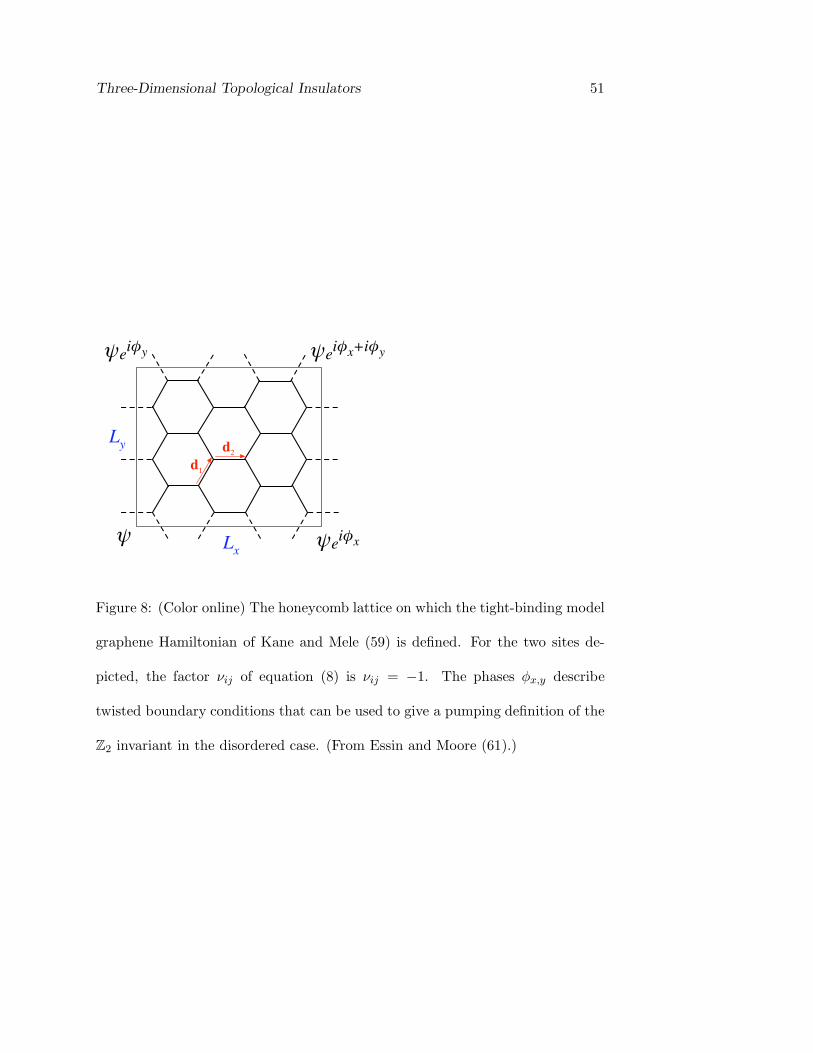
Three-Dimensional Topological Insulators 51
Ly
Lx
!!
!"
ψeiφx
ψeiφx+iφyψeiφy
ψ
Figure 8: (Color online) The honeycomb lattice on which the tight-binding model
graphene Hamiltonian of Kane and Mele (59) is defined. For the two sites de-
picted, the factor νij of equation (8) is νij = −1. The phases φx,y describe
twisted boundary conditions that can be used to give a pumping definition of the
Z2 invariant in the disordered case. (From Essin and Moore (61).)
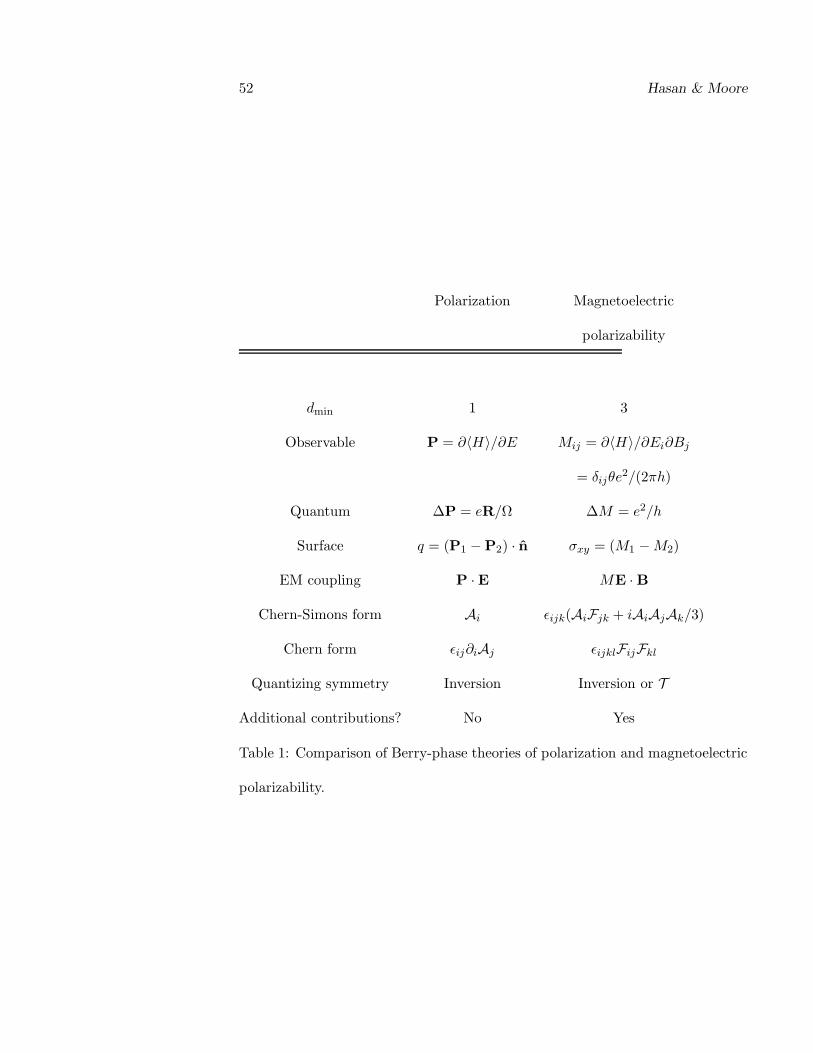
52 Hasan & Moore
Polarization Magnetoelectric
polarizability
dmin 1 3
Observable P = ∂〈H〉/∂E Mij = ∂〈H〉/∂Ei∂Bj
= δijθe2/(2πh)
Quantum ∆P = eR/Ω ∆M = e2/h
Surface q = (P1 −P2) · n σxy = (M1 −M2)
EM coupling P ·E ME ·B
Chern-Simons form Ai ǫijk(AiFjk + iAiAjAk/3)
Chern form ǫij∂iAj ǫijklFijFkl
Quantizing symmetry Inversion Inversion or T
Additional contributions? No Yes
Table 1: Comparison of Berry-phase theories of polarization and magnetoelectric
polarizability.

Three-Dimensional Topological Insulators 53
Majorana states
SC
TI
Figure 9: (Color online) The creation of Majorana fermions in the layer of un-
conventional superconductivity between an ordinary s-wave superconductor and
a topological insulator (90). A vortex core traps one Majorana fermion mode in
its vicinity at each interface.