
Design, Fabrication and Characterization of One Dimensional ...

1
Three Dimensional Modeling and Characterization
for Die Attach Process
Lin Bu, Wai Leong Ching, Ho Siow Ling, Minwoo Rhee, Yong Puay Fen
1
Abstract: A new three dimensional model for the die
attach (DA) process is established and validated in the
present study. With this model, the fluid flow
characteristics of the DA process can be predicted
accurately. Dynamic mesh and interface tracking method
were adopted in the modeling to study the compression
motion and the front of DA. Force driven model was
conducted for the parametric studies of different bonding
force. The model for the DA process was validated by the
four materials, AP1, CA1, CA4 and DM60 in the
optimized condition. Bond line thickness (BLT) can be
predicted by simulation with ~20% accuracy. The
simulation results show that viscosity is one of the key
properties, which has a significant effect on the required
bonding force, bonding time and DA contamination on the
die top. Complete filling and DA contamination on the die
top are two important standards to evaluate the good
bonding force range in fluid dynamic analysis. Stress
analysis illuminates that fillet area is very critical and
experiences highest stress during the reflow process.
Index Terms — die attach process, bond line thickness
(BLT), bonding force
I. INTRODUCTION
ie attach provides the mechanical support between the
silicon die and the substrate, i.e,. leadframe, plastic or
ceramic substrate. The die attach is also critical to the
thermal and, for some applications, the electrical performance
of the device. Significant results have been achieved in
previous studies, focusing on mechanical analysis for the DA
process. Dynamic mechanical analysis (DMA) was employed
to characterize the modulus behavior of silver filled glass
material. The method used a simulated DA process to
understand the behavior of the storage modulus and the
complex viscosity [1]. DMA taking into account multi-step
curing was utilized to determine gelation times and melt
viscosity under a shear mode by Taweeplengsangsuke J. [2].
They found that the longer the period of time at the lower
temperature step of the 2-step curing gave rise to lower cure
stress. In addition, the stress during the cool down process was
investigated. At the point of decreasing temperature, the stress
dramatically increases. The higher temperature difference, the
larger the residual stress. Xiaosong M. et al. [3] developed a
finite element model to predict the interface delamination
1The authors are with the Institute of Microelectronics, Agency for
Science, Technology and Research, 117685, Singapore.
Corresponding author is Min Woo Rhee. (e-mail: [email protected]
star.edu.sg; [email protected]; [email protected];
[email protected], [email protected]).
issues encountered in the DA process. It is found that
temperature has a large effect on the interface toughness (Gc).
Gc greatly decreases with increasing temperature. In addition,
moisture has no effects on interface toughness of copper and
silver filled DA in their samples. Khoo Ly Hoon [4] et al.
aimed to establish a robust DA process by evaluating various
responses on DA epoxy with various values of epoxy
viscosity. The findings of their study reveal that the epoxy
viscosity within the tested range does not significantly affect
DA and wire bond performance. Nicolas Heuck et al.[5]
investigated the impact of the CTE of die-attach layers on the
thermal stress in chip and attach layer, along with strategies to
reduce the CTE of conventional silver sintered die-attach
structures by adding materials like SiC or h-BN. They found,
that the implementation of SiC and especially of h-BN
additives in 200μm thick sintered silver die-attach layers can
lead to a stress reduction up to 30%.
However, rheological simulations that can investigate the
flow of the liquid DA under an applied force during the DA
process are rare. In order to enhance the evenness of epoxy
distribution along the peripheral of the die, Mark Lee [6] built
a 2D model to investigate various dispensing patterns and to
study their evolvement patterns. The thin-film assumption is
used in the simulations. The studies shows that a suitable
epoxy pattern is the key to ensure that the epoxy dispensed on
the substrate can evolve to the final shape of the chip after the
initial squeezing during the DA process. Complex dispensing
patterns, i.e. snow star pattern are more likely to trap voids
than basic dispensing pattern, i.e. x dispensing pattern.
However, 2D simulation cannot capture the 3D real process
very well and many important properties like surface tension
and contact angle are not incorporated into the model.
Important information such as BLT and contaminations on the
die top in the DA process could not be obtained due to 2D
constraint. The prediction of final BLT and die top
contaminations are as important as epoxy dispensing patterns.
Final BLT would have a significant effect on the reliability of
the whole system. Man Wai Chan [7] et al. invented a way to
measure BLT with laser equipment. They can also control
BLT in a desired range by adjusting the four parameters, 1)
adhesive dispensing pressure of the dispenser, 2) bond level of
the bonding tool, 3) bond force exerted by the bonding tool
and 4) bond delay of the bonding tool.
In the present study, rheological simulations were carried
out using the three dimensional model. Surface tension model
and wall adhesion model are enabled to take into account the
effect of surface tension along the interface of two fluids and
the contact angle that the fluid makes with the wall.
Appropriate bonding force and BLT ranges for the
optimization of DA process can also be predicted by the
present model.
D

2
II. PACKAGE DESCRIPTION AND CRITICAL ISSUES
DURING DA PROCESS
Institute of Microelectronics at A*STAR Singapore and its
industry partners have developed a DA technology, based on a
5×5 mm2 top chip. Fig. 1 demonstrates a schematic plot of DA
process.
Fig. 1. Schematic plot of DA process
The DA process consists of three stages. First stage is to
dispense an adhesive with a dispenser onto the substrate.
Then, in the second stage, a semiconductor die is picked and
placed on the adhesive which has been dispensed onto the
substrate with a bonding tool with vacuum. Thereafter, in the
third stage BLT between the bottom surface of the
semiconductor die and top surface of substrate on the process
platform using a measuring device.
(a) Overflow
(b) Incomplete fill
Fig. 2. Schematic plot of DA issues. (a) Overflow. (b) Incomplete fill.
During the second stage, void issue, bad fillet and
contamination on the die top are the key issues. Epoxy
climbing along the edge of the die will lead to the formation of
DA fillet. Excessive DA fillet can lead to DA contamination
of the die surface. Too little of it may lead to die lifting and
die cracking. These two issues are demonstrated in Fig.2.
Voids maybe trapped by using inappropriate dispensing
patterns. Voids in the epoxy not only increase thermal and
electrical resistance, but also trigger electrical breakdown at
extreme conditions. Overcoming these three issues is a
balance of controlling dispensing pattern, bonding force and
bonding time.
III. GOVERNING EQUATIONS
The equation for the conservation of mass, or continuity
equation, shared by the two phases, can be written as follows
[8],
( ) (1)
Conservation of momentum in an inertial (non-accelerating)
reference frame, also shared by the two phases, is described
by,
( ) ( ) ( ) (2)
Where p is the static pressure, is the stress tensor, and
is the gravitational body. represent the surface tension
force by CSF (continuum surface force) model provided by Brackbill
et al, [9].
The energy conservation equation, still shared by the two
phases, is as follows,
( ) ( ( )) ( ) (3)
The VOF model treats energy, h, and temperature, T, as
mass-averaged variables. The properties and keff (effective
thermal conductivity) are shared by the phases.
The compressible fluid complies the idea gas law,
(4)
The transport equation is determined by,
( )
( ) (5)
{
The properties appearing in the transport are determined by
the presence of the component phases in each control volume.
In a two-phase system, if the phases are represented by the
subscripts l and g, the density in each cell is given by,
( ) (6)
IV. MATERIAL CHARACTERIZATION
A. Viscosity measurement and characterization
Viscosity is one of the key properties which will have a
significant effect on the finial BLT and bonding time. Power
law was used to characterize the viscosity of epoxy, as shown
in equation (7):
μ=γ1-n
(7)
Where and n are input parameters. is a measure of the
average viscosity of the fluid (the consistency index); n is a
measure of the deviation of the fluid from Newtonian (the
power-law index). The value of n determines the class of the
fluid (i.e. Newtonian fluid, dilatants fluids or pseudo plastics).
The time dependent viscosity is measured by the fluid
viscometer. In the non-Newtonian phenomenon, viscosity
deceases with share rate for four corresponding materials, as
shown in Fig.3. Subsequently, the measurement results are
Pick up tool
Substrate
DA
Top chip

3
characterized with power law trend line. and n are finally
determined and put into software for modeling setup. In the
experiment, the shear rate is from 1-100 1/s at room
temperature. In the simulation, we also set up the min. and
max viscosity according to the experiment. In the very low
shear rate region, we redeem the material as shear rate
independent.
Fig. 3. Viscosity measurement results
B. Contact angle measurement
A contact angle can be measured by producing a drop of
liquid on a solid. The angle formed between the solid/liquid
interface and the liquid/vapor interface is referred to as the
contact angle. The most common method for measurement
involves looking at the profile of the drop and measuring two-
dimensionally the angle formed between the solid and the drop
profile with the vertex at the three-phase line as shown in Fig.
4 and table 1. Young's equation is used to describe the
interactions between the forces of cohesion and adhesion and
measure what is referred to as surface energy. Due to epoxy is
not an isotropic medium, the measurement results were
collected from different directions. The averaged contact angle
for different materials is imported into software as the
modeling input. Fig.5 lists the average contact angle for the
different combination of three epoxies and two material
metallization. Hydrophilic angles (<40˚) were observed for all
the alliances, which ensures qualified wetting and adhesive for
the DA procedure.
Fig. 4. Contact angle measurement result
Table 1 Contact angle measurement result
Unit R L
CA1 (SiN) 1 24.5o
26.5o
2 25o
27o
DM60 (SiN) 1 13o
13o
2 10o
23o
AP1 (SiN) 1 24.5o
25.5o
2 18o
24o
AP1 (Si-Ag) 1 48o
33o
2 29o
30o
Fig. 5. Average contact angle
V. MODELING
In order to further understand the DA process,
computational fluid dynamics (CFD) simulation is a valuable
tool. However, establishing a validated model is a challenging
task. In this paper, a 3D finite volume model was established,
as shown in Fig. 6. The evolution of the epoxy front is tracked
by the Volume of Fluid (VOF) [10] method. The modeling
consists of the following assumptions:
1. Quater model is adopted to save computation efforts.
2. In the experiment as well in the simulation, there are two
ways of controlling the travel of the die. (1) Velocity
controlling: with velocity and time controlling, the
ultimate overtravel length and final BLT could be
determined. (2) Force controlling: force controlling can’t
determine the overtravel length at the initial time. Final
BLT depended on the balance of the applied bonding
force, gravity force and surface tension force.
3. Bonding force could be applied by user defined functions
(UDF). With impropriate bonding force profile, mesh
collapse will be easily encountered.
4. The curing of the DA material is not considered.
y = 4.4011x-1.025
y = 87.144x-0.616
y = 10.069x-0.86
y = 2.1507x-0.651
0.01
0.1
1
10
100
1.00 10.00 100.00
Vis
cosi
ty (
Pas
)
Shear rate (1/s)
AP1
CA4
CA1
DM60
0
5
10
15
20
25
30
35
40
CA1 on SiN DM60 onSiN
AP1 on SiN AP1 on Ag
Ave
rage
co
nta
ct a
ngl
e (
°C)

4
(a)
(b)
Fig. 6. 3D modeling of DA process. (a) x dispensing pattern. (b) Boomerang
dispensing pattern
VI. VALIDATION
The model for the DA process was validated for the four
materials in the optimized condition. The experiments and the
simulation data matched very well, as shown in Table 2. The
four materials with different properties and different bonding
forces proved the feasibility of the model in a wide range.
BLT can be predicted by the simulation with less than 20%
errors. Table 2 Comparison of BLT between experiment and modeling
Input parameters (temperature fixed as 25°C)
Results
Material
Density
Dispensing weight
Bonding force
Dispensing
pattern
Experiment
Modeling
CA4 6g/cm3 4.6mg 60g x 28.5m 24.7m
CA1 4.4g/c
m3
4.33mg 28g x 28.5m 26.7m
DM60
4.5 g/cm3
2.98mg 21.75g x 28.87m 21.5m
AP1 4.2229g/cm3
4.43mg 43.5g
Boomerang
32.5m 31.7m
In order to further validate the model, the visual inspected
die attach final filler shape was examined at two locations
shown in Fig.7. Fig.8 shows the validation results through
modeling and experiment for material CA4, CA1, DM60 and
AP1. The contaminations at location 1 for the four cases show
the prediction results are in good accordance with the
experiment. A concaved feature was perceived at location 2 by
using material AP1 with boomerang dispensing pattern. This
phenomenon is captured in experiment as well as the
simulation result, as shown in Fig.8 (d). For the other cases,
the model using x dispensing pattern, the filler shape is
comparatively straight.
Fig. 7. Inspected locations
(a)
(b)
(c)

5
(d)
Fig. 8. Validation results through modeling and experiment. (a)CA4.(b)CA1.
(c)DM60. (d)AP1
VII. RESULTS AND DISCUSSION
A. Effect of dispensing pattern
Dispensing pattern is very important during the die attach
process. The key difficulty is that the square shape of the die is
not easy for full filling. There are four criterions to judge a
proper dispensing pattern: (1) even and strong fillet; (2) little
or no contamination on die top; (3) high coverage.
In experiment, x dispensing pattern (A) and star dispensing
pattern (B&C) with material CA1, was tried first to observe
the coverage and the fillet, as shown in Fig.9. Dispensing B &
C was observed heavy wavy fillet coverage. After curing, the
fillet will has some shrinkage. Dispensing pattern A was
decided to use to do further work. In the simulation, the results
should have a strong fillet due to curing was not included in
the simulation.
Fig.9 Experimental results of x and star dispensing pattern
Excess materials were observed at four corners at the die for
dispensing pattern A with an overtravel length of 50um.
Simulation was conducted in the meanwhile to confirm this
phenomenon.
Fig.10 reveals the transient histories of the DA melting
front with an x dispensing pattern. At the initial state, as
shown in Fig.10 (a), the DA material was dispensed like an
“x” shape. As the time went on, the melting front evolved
from the central to the peripheral of the chip. Ultimately, as
shown in Fig.10 (d), DA material fully filled the chip.
(a)
(b)
(c)
(d)
Fig. 10. Time dependent simulation results for CA1.(a) t=0ms. (b) t=40ms. (c) t=70ms. (d) t=80ms.
Fig. 11. Comparison of experiment and simulation with x dispensing pattern

6
Once the simulation was validated by the experiment, as
shown in Fig.11. Further investigation should be done to
improve the process.
Fig.12 Three parameters for optimization
Three parameters, A, W and D, could be optimized regarding
to x dispensing pattern in the simulation, as shown in Fig.12.
After a series of simulation have been done, A/W/D was
finalized as 7.11mm/1.23mm/0.386mm, as shown in Fig.13.
Fig.13 x pattern before and after optimization
For material CA1, CA4, DM60, both experiment and
simulation shows good coverage with x dispensing pattern.
The x-ray image after die attach with full material coverage
was also shown in literature [11].
For material AP1, incomplete epoxy coverage at 1/3 length
from corner was detected from x-ray image. Thus, boomerang
dispensing pattern was used to meet the coverage requirement.
Fig. 14 shows the transient histories of the DA melting front
with a boomerang dispensing pattern in simulation. Four
additional volumes of DA that resemble “v” shape were added
to the edge of the substrate in order to get a full coverage, as
shown in Fig. 14 (a). The edge of the additional volume and
“x” was joined as the time went on and moved together
towards the edge of the top chip, as shown in Fig. 14 (d). Full
coverage was achieved and the revised pattern is sufficient to
meet the target. At the joint part of “v” and “x”, a concaved
feature could be observed.
(a)
(b)
(c)
(d)
Fig. 14. Time dependent simulation results for AP1. (a) t=0ms. (b) t=2ms. (c)
t=3.3ms. (d) t=6.5ms.
Boomerang dispensing pattern found slight void in the
simulation results, which is less than 1%. However, in the real
case, the migration of metal induced porosity is much higher
than the process induced porosity [11], as shown in Fig.15.
Fig.15. Porosity of AP1 material [11]

7
The Scanning Electron Microscope(SEM) image was shot
at different cross sections. With 5mm×5mm die size, the
porosity in some area is larger than 10%.
Fig.16. Cross section image from experiment [11]
Table 3 Fillet height and BLT in the experiment
Fillet
Height
(L)
Fillet
Width
(L)
BLT (L) Fillet
height
%(L)
BLT (R) Fillet
height (R) Fillet
Width
%(R) 64um 138um 33um 62% 36.5u
m 62um 51%
111um 135um 27.5um 47% 23um 130um 61%
Fig.16 reveals the cross section result for two different die
thicknesses, i.e., 50um and 175um. No voids or delamination
was perceived during the experiment. The fillet height ratio
ranges from 47%-62%. In simulation, the most critical area
with low fillet occurs at the central of the die edge for x
dispensing pattern. However, the low fillet area appears at 1/3
length from die corner for boomerang dispensing pattern.
In literature [12], fillet height range from 0%-75% was
studied, 0% fillet height was observed with the worst
delamination. For the fillet height above 0%, higher fillet is
generally having more delamination after TC and MSL test.
Some delamination was found at 75% fillet height. In our
reliability test, only very low fillet has the delamination issue.
Fig.17 shows the delamination at die edge with 1000 hours
high temperature storage (HTS) test with DA material AP1.
The cross section image at center of the package was taken
after HTS test, the fillet height could be deducted that it was
also not good at 0 time. Fig.18 revealed some delamination
between underfill and leadframe with DA material DM60 after
MSL3 test. The fillet was also in the worst condition, near 0
fillet.
Fig.17 DA delamination at DA fillet area after HTS1000
Fig.18 Delamination between underfill and leadframe after MSL3 test
B. Fluid analysis with force control
(a)
(b)
Fig.19. Effect of bonding force in the DA process. (a) Bonding force window with fluid analysis. (b) BLT range for good DA.
From the simulation results, the bonding force process
window was extracted to provide the process optimization.
Fig.19 (a) displays the relationship between the DA coverage
on die top and substrate vs. bonding force for AP1 in the
optimized condition. It can be seen that complete filling was
obtained when the bonding force range falls above 10g. The
DA contamination on the die top was always above 0%.
Fig.19 (b) illustrates the corresponding BLT range at different
bonding force. As the bonding force increase, DA
contamination on the die top and DA coverage on the
substrate will increase along with it. However, increasing of
0.0%
0.1%
0.2%
0.3%
0.4%
0.5%
80%
85%
90%
95%
100%
0 10 20 30 40 50 60 70 80 90
DA
co
vera
ge o
n d
ie t
op
DA
co
vera
ge o
n s
ub
stra
te
Bonding force /g
0
20
40
60
80
30 32 34 36
Bo
nd
ing
forc
e /
g
BLT /um

8
bonding force will lead to decreasing of BLT. With force
control of very thin die as 50um, contamination on the die top
is hard to control. Thus, position control was used to make a
good fillet height [11].
C. Stress analysis for DA process
Fig.20 Stress (MPa) variation along the edge of the DA at DA BLT equals to
10um, 20um, 30um and 40um.
Investigating the stress level at the DA in the vicinity of the
edge of the DA, it can be observed that stress increases
towards the corner of the DA for all the thicknesses
investigated. It is evident that the die attach fillet area is most
critical, as shown in Fig.20. In this area, silicon die, die attach
material, substrate and backside metallization are
concentrated. Highest CTE (coefficient of thermal expansion)
mismatches are experienced during the die attach process and
later on molding and reflow process. In the reliability test, like
HTS (high temperature storage), TC(thermal cycling), die
edge area has high possibility leading to failure. During MSL
reliability test, the edge area also experiences the highest CME
(coefficient of moisture expansion) mismatch as well.
Also, it is obvious that increasing the thickness of the DA
material is favorable in reducing the amount of DA stress in
the package. Although the DA candidates investigated
comprised mainly of silver sintering material, the metallic DA
is more compliant as compared to silicon and leadframe and
increasing its thickness will help to introduce more
compliance thereby reducing DA stress. Mechanical
simulations suggest that a higher BLT is more desirable in
reducing the DA stress.
The detailed process dependent modeling was elaborated in
[13]. Four process steps are simulated, namely, die attach
process at 25ºC, molding process at 175ºC, cooling down to
room temperature at 25ºC and reflow process at 260ºC. The
most critical process is reflow process, which leads to the
highest stress in die attach material.
VIII. CONCLUSION
The 3D DA numerical simulation has the advantage of
giving a deep insight into the DA flow mechanism. Some
important conclusions and recommendations from this paper
can be summarized as follows.
(1) Amongst all the material properties, viscosity is one of the
dominant factors in the DA process. It has a significant
effect on the required bonding force, bonding time and
DA contamination on the die top. Most of the time, the
material property is temperature dependent. The viscosity
of the DA material could be adjusted by pre-heat of the
substrate.
(2) Two kind of dispensing patterns were considered in the
modeling, i.e. x dispensing pattern and boomerang
dispensing pattern. Two patterns are used for different
materials. For material CA1,CA4, DM60, no abnormity
was observed during the experiment. Boomerang
dispensing pattern was used to solve the incomplete fill
issues encountered for material AP1.
(3) With ultra-thin die as 50um, force control is very hard to
control the final fillet height and contamination on the die
top. Position control is more favorable in controlling the
two.
(4) For x dispensing pattern, simulation shows that in the
central of die edge, low fillet has higher possibility to
occur. The most dangerous/low fillet location could be
changed to 1/3 length from die corner for boomerang
dispensing pattern.
(5) Fillet area is the most critical area in the die attach
process. Highest CTE and CME mismatches are
experienced during the die attach process and later on
molding and reflow process. In the reliability test, die
edge area has high possibility leading to failure.
(6) Mechanical simulations suggest that a higher BLT is more
desirable in reducing the die attach stress. The highest
stress appears at reflow temperature.
ACKNOWLEDGMENTS
This work has been carried out as part of the 11th
Electronics Packaging Research Consortium (EPRC-11) led
by the Institute of Microelectronics (IME), a research institute
of the Agency for Science, Technology and Research
(A*STAR). The members of the consortium include
GLOBAL FOUNDRIES, HERAEUS, INFINEON Co. Ltd.,
NXP Pte Ltd, OPTITUNE Pte Ltd, and ROLLS-ROYCE Pte
Ltd. The authors are grateful to members of EPRC 11 –
EMWLP Project as well as IME staffs who had contributed
and made this work possible.
REFERENCES
[1] Trirat Hongsmatip. “Dynamic Mechanical Analysis of
Silver/Glass Die Attach Material,” Electronic
Components and Technology Conference, pp.692-700,
1995.
[2] J. Taweeplengsangsuke, J.C. Hsiung, and R.A. “Modeling
the Die Attach Adhesive Process,” International
symposium on advanced packaging materials, pp. 165-
169, 1998.
[3] Xiaosong Ma, G.Q. Zhang and O. van der Sluis, et al.
“Die Attach Interface Property Characterization as
Function of Temperature using Cohesive Zone Modeling

9
Method,” 11th. Int. conf. on Thermal, Mechanical and
Multiphysics Simulation and Experiments in Micro-
Electronics and Micro-Systems, pp. 1-8, 2010.
[4] Khoo Ly Hoon, Au Yin Kheng. “In-Depth
Characterization of Die Attach Adhesive for Low-K
Automotive Device Application,” 11th Electronics
Packaging Technology Conference, pp. 977-981, 2009.
[5] Nicolas Heuck, Armin Langer and Andrej Stranz, et al.
“Analysis and Modeling of Thermomechanically
Improved Silver-Sintered Die-Attach Layers Modified by
Additives,” IEEE transactions on compounents,
packaging and manufacturing technology, Vol. 1, pp.
1846-1855, 2011.
[6] Mark Lee, “The Squeezing Process of Complex Epoxy
Patterns in the Die-attaching of Large IC-Chip,”
International Conference on Electronic Materials and
Packaging, pp.1-8, 2006.
[7] Man Wai Chan, Shiu Kei Lam, Wan Yin Yau, Kwok
Yuen Cheung, Bond Line Thickness Control for Die
Attachment,” Patent US20130011941 A1, 2013
[8] Rohsenow W. M., Hartnett J.P., Garnic E.N., “Handbook
of Heat Transfer Fundamentals”. 2nd ed. New York:
McGraw-Hill, 1985
[9] J.U.Brackbill, D.B.Kothe, C. Zemach., “A continuum
method for moeling surface tension.” J.Comp..Phys., Vol
100, pp. 335-354, 1992.
[10] C. W. Hirt, B. D. Nichols, “Volume of Fluid (VOF)
Method for the Dynamics of Free Boundaries,” J. Comp.
Phys., Vol.39, pp. 201–225, 1981.
[11] Leong Ching Wai, Ding Mian Zhi, Vempati Srinivasa
Rao, Min Woo Daniel Rhee, “Process Characterization of
Highly Conductive Silver Paste Die Attach Materials for
Thin Die on QFN”, Electronic Packaging and Technology
Conference, pp.372-378, 2012.
[12] Raymund Y. Agustin, The Effect of Glue Bond Line
Thickness (BLT) and Fillet Height on Interface
Delamination, ASEMEP National Technical Symposium,
pp.1-6, 2015.
[13] Ho Siow Ling, Leong Ching Wai, Germaine Hoe Yen Yi,
Min Woo Daniel Rhee, “Impact of Advanced Materials
on Power Cycling Performance and Process Dependent
Stresses of QFN”, Electronic Packaging and Technology
Conference, pp.119-124, 2012.
10
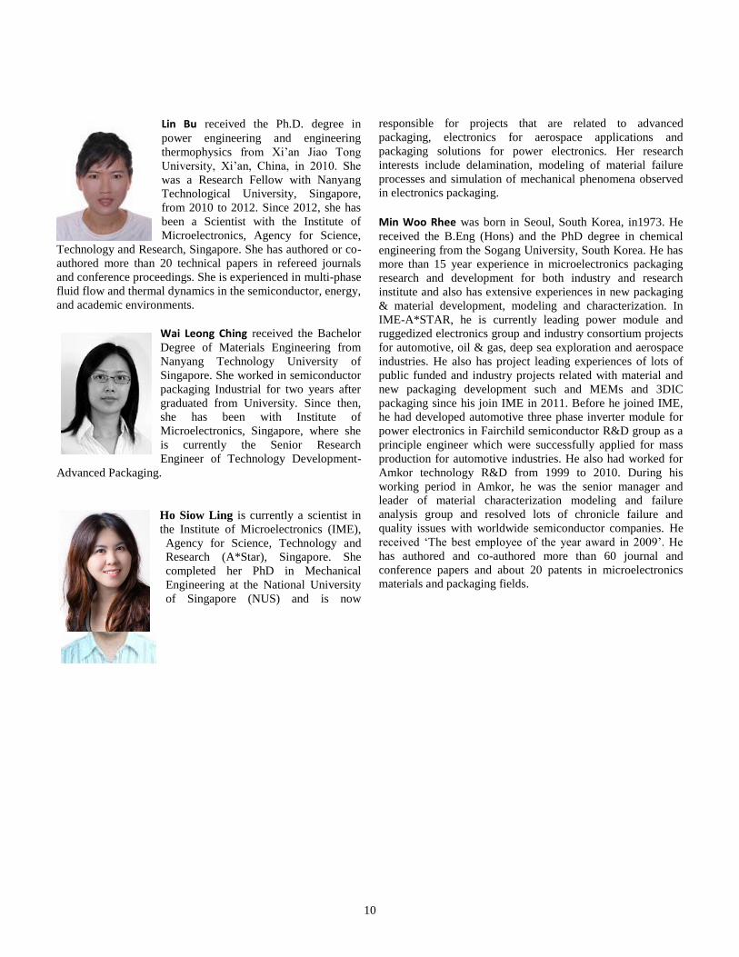
Lin Bu received the Ph.D. degree in
power engineering and engineering
thermophysics from Xi’an Jiao Tong
University, Xi’an, China, in 2010. She
was a Research Fellow with Nanyang
Technological University, Singapore,
from 2010 to 2012. Since 2012, she has
been a Scientist with the Institute of
Microelectronics, Agency for Science,
Technology and Research, Singapore. She has authored or co-
authored more than 20 technical papers in refereed journals
and conference proceedings. She is experienced in multi-phase
fluid flow and thermal dynamics in the semiconductor, energy,
and academic environments.
Wai Leong Ching received the Bachelor
Degree of Materials Engineering from
Nanyang Technology University of
Singapore. She worked in semiconductor
packaging Industrial for two years after
graduated from University. Since then,
she has been with Institute of
Microelectronics, Singapore, where she
is currently the Senior Research
Engineer of Technology Development-
Advanced Packaging.
Ho Siow Ling is currently a scientist in
the Institute of Microelectronics (IME),
Agency for Science, Technology and
Research (A*Star), Singapore. She
completed her PhD in Mechanical
Engineering at the National University
of Singapore (NUS) and is now
responsible for projects that are related to advanced
packaging, electronics for aerospace applications and
packaging solutions for power electronics. Her research
interests include delamination, modeling of material failure
processes and simulation of mechanical phenomena observed
in electronics packaging.
Min Woo Rhee was born in Seoul, South Korea, in1973. He received the B.Eng (Hons) and the PhD degree in chemical
engineering from the Sogang University, South Korea. He has
more than 15 year experience in microelectronics packaging
research and development for both industry and research
institute and also has extensive experiences in new packaging
& material development, modeling and characterization. In
IME-A*STAR, he is currently leading power module and
ruggedized electronics group and industry consortium projects
for automotive, oil & gas, deep sea exploration and aerospace
industries. He also has project leading experiences of lots of
public funded and industry projects related with material and
new packaging development such and MEMs and 3DIC
packaging since his join IME in 2011. Before he joined IME,
he had developed automotive three phase inverter module for
power electronics in Fairchild semiconductor R&D group as a
principle engineer which were successfully applied for mass
production for automotive industries. He also had worked for
Amkor technology R&D from 1999 to 2010. During his
working period in Amkor, he was the senior manager and
leader of material characterization modeling and failure
analysis group and resolved lots of chronicle failure and
quality issues with worldwide semiconductor companies. He
received ‘The best employee of the year award in 2009’. He
has authored and co-authored more than 60 journal and
conference papers and about 20 patents in microelectronics
materials and packaging fields.


