
This presentation was provided by Andrew Cole to the … · This presentation was provided by...
20
1 This presentation was provided by Andrew Cole to the Design & Reuse IPSoC Symposium in Shanghai, September 15, 2015
Transcript of This presentation was provided by Andrew Cole to the … · This presentation was provided by...

1
This presentation was provided by Andrew Cole to the Design & Reuse IPSoC Symposiumin Shanghai, September 15, 2015

This presentation is about a problem we at Silicon Creations have seen quite often when our, or others’ PLLs are used in complex SoCs. Although the design team usually implements the PLL correctly in the chip with the right supplies connected the right ways, we have often seen that designers overlook the significant impact that their floorplan and power supply plan have on the clock as it travels from the PLL to the circuits the PLL is clocking. This is the impact of the SoCsupply noise on the quality of the clock. Because of this we have often helped our customers to understand this issue to ensure their chip works first time, or help them understand how to repair an SoC when they have made mistakes in the design. Our Application notes do include lots of guidelines for this, but we often have to explain this in person or over a WebEx session. Drawings and whiteboards are always helpful, and we’ve made a few short presentations in the past. For the forum today we decided to pull this material together to a presentation we think we will be useful to at least some of you.
The supply noise in SoCs hurts the clock by creating jitter. This jitter is important because it reduces timing margin and can limit the speed of logic circuits or even cause them to fail. When the clock is used for SerDes the jitter can prevent the SerDes from operating as fast as it should. And the jitter can also be seen as distortion so that the SNR of clocked analog circuits is too low.
This presentation talks about jitter, the mechanism that causes this additional jitter on SoCs, how you can simulate this and what you can do about it.
2

Here is an outline of our presentation.
We spend a minute telling you about our company.
And then we cover the topics mentioned. We start by talking about different kinds of jitter and what matters for various kinds of circuits.
Then we’ll get to how supply noise causes CMOS gates and buffers to create jitter (or not –because it doesn’t always happen).
The we talk about how to estimate and simulate how much jitter is added.
And finally we talk about a few techniques you can use to reduce or avoid this jitter
3

Silicon Creations is a small company founded in 2006 and focuses on precision timing and high-speed interface circuits. Our IP is in production from 16nm to 180nm and taping out soon in 10nm. We have been serving Chinese companies since 2006 and this is a very important market for us.
Our two main product lines are PLLs and SerDes.
Our most popular PLL is an extremely wide range and highly programmable Fractional-N, Current Starved Ring PLL that has lower jitter in Fractional mode than most people’s integer PLLs. It’s a one-size-fits-98%-of-the-Chips PLL.
We have variants with even lower jitter.
We also have a rapidly growing range of SerDes products for a number of consumer standards and Semi-Custom applications, mostly operating below 10Gbps, and are currently testing a 12.7Gbps multi-protocol PHY. Our key selling point here is we can use our high quality ring oscillator circuit from our PLLs to meet jitter requirements beyond 10Gbps and only require a Crystal reference.
You can visit our website for more information.
4

So, we’re now getting to the meat of the presentation.
First let’s talk about different kinds of jitter. The picture shows what you might see if you trigger an oscilloscope on the rising edge of a clock. Many oscilloscopes allow you to generate a histogram of crossing points for a rising edge after the trigger. If you look at the histogram for the first rising edge you are measuring the period jitter. If you look at the histogram of the second edge you are looking at the 2-cycle jitter which is the same as the calculated difference between the first and second periods and is also called the cycle-cycle jitter. If only random jitter is present you will see nice Gaussian shapes, commonly called “bell curves” and the Gaussian of the 2-cycle jitter, or cycle-cycle jitter will be sqrt(2) wider than the period jitter. If we keep delaying the point where we generate the histogram to comfortably more than 1/BW of the PLL we will measure what is called the Long term jitter.
5

If you measure all the N-cycle jitter points and plot them on a graph, with the Y-axis being the standard deviation of the Gaussian distributions measured and the X-axis being the log of N or the log of the hold-off time, you will see a line that initially rises linearly, then flattens off and eventually rises again.
The green annotations now shown on the lines show the source of these three regions. For small N’s the time is too short for the PLL to control any deviations. It’s essentially the open loop response of the PLL and caused by the VCO noise. As the curve flattens out we see a region where the PLL closed loop feedback mechanism dominates. This is very nearly flat in most modern PLLs and you can measure the long term jitter almost anywhere here. And eventually we get to the region where the reference clock is wandering around and the fact that the PLL follows this slow input noise dominates.
Unfortunately in most systems there is too much noise for us to measure the period jitter or cycle jitter. There is a jitter noise floor that comes from somewhere else.
This noise is called deterministic jitter and comes from a number of sources that are listed here.
6
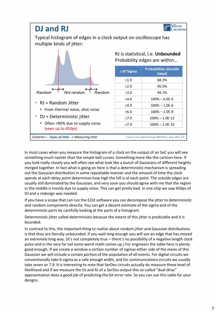
In most cases when you measure the histogram of a clock on the output of an SoC you will see something much nastier than the simple bell curves. Something more like the cartoon here. If you look really closely you will often see what look like a bunch of Gaussians of different heights merged together. In fact what is going on here is that a deterministic mechanism is spreading out the Gaussian distribution in some repeatable manner and the amount of time the clock spends at each delay point determines how high the hill is at each point. The outside edges are usually still dominated by the Gaussian, and very soon you should agree with me that the region in the middle is mostly due to supply noise. This can get pretty bad. In one chip we saw 450ps of DJ and a redesign was needed.
If you have a scope that can run the EZJit software you can decompose the jitter to deterministic and random components directly. You can get a decent estimate of the sigma and of the deterministic parts by carefully looking at the parts of a histogram.
Deterministic jitter called deterministic because the extent of this jitter is predicable and it is bounded.
In contrast to this, the important thing to realize about random jitter and Gaussian distributions is that they are literally unbounded. If you wait long enough you will see an edge that has moved an extremely long way. (It’s not completely true – there’s no possibility of a negative length clock pulse and in the very far tail some weird math comes up.) For engineers the table here is plenty good enough. If we create a window a certain number of sigmas either side of the mean of this Gaussian we will include a certain portion of the population of all events. For digital circuits we conventionally take 6-sigma as a safe enough width, and for communications circuits we usually take seven or 7.9. It is interesting to note that SerDes circuits actually do measure these level of likelihood and if we measure the DJ and RJ of a SerDes output this so-called “dual dirac” approximation does a good job of predicting the bit error rate. So you can use this table for your designs.
7

As mentioned earlier, there are different kinds of jitter and not all circuits care about all kinds of jitter.
Generally digital circuits care about the period jitter because that determines the shortest period they will see, and so the period jitter affects the timing margin the designers need to account for. The period jitter that matters for timing margin is the one-sided deterministic period jitter plus the peak random period jitter. Since random jitter is not bounded we use a statistical number times the sigma of the Gaussian (or RMS jitter). In digital; circuits we usually use 6 sigma for the one sided peak.
Other circuits like AFEs, DACs, SerDes and often RF communications circuits usually care about long term jitter. Usually the random long term jitter dominates the performance but, the deterministic jitter can’t always be ignored here. The calculations are often a little complicated but the better IP vendors can help you with them.
8

If you have a fast oscilloscope with an accurate time-base it is likely you can run the EZJitsoftware on the scope. This software can gather a jitter histogram and decompose it to a composite of random jitter and deterministic jitter. If you know the bandwidth of the PLL you can also estimate PJ from the LTJ random histogram. And you can measure with the PLL in bypass or active to see which parts come from the PLL and which from the rest of the system.
You can also use the histogram function of the same oscilloscope and estimate the deterministic portion and the one-sigma value of the “bell curves” in the composite histogram. Often your estimate of the one-sigma value is close and this is the RMS jitter. This method is fast.
There are more elaborate ways of measuring jitter using a Phase Noise or Spectrum Analyzer.
9

This nice colored graph is a normalized map of CMOS gate delays for a 28nm process. The blue square in the middle is normalized to 100%. The top section is SS process, the middle typical process and the bottom is FF. Horizontally we go from -25% supply voltage (as many of us now use) up to +15%.
You can see from the nifty coloring that the delay gets smaller with increasing voltage and with increasing temperature (which is true for most advanced processes). This is not at all a surprise to any of us. That’s why we close timing over PVT corners.
If we move from the conventional SS, -10% supply to FF, +10% the gate delay changes by 2.5X, and if we go over the whole extent of the range the delay changes by 10X!
The most important message in this slide is that the gate delay changes with supply voltage. So if the supply voltage changes quickly (while a clock edge is inside a clock tree) the clock edge will be moved faster or slower. This means the edges will come out of a clock tree that has a noisy supply with period jitter, even if they were perfectly clean going in.
There’s a handy formula here that is quite often true so we come back to it in more detail later. But what is says is the amount the clock edge is moved is roughly equal to the delay of the clock tree times the change in the supply voltage divided by the nominal supply voltage adjusted by the transistor threshold voltage.
10

Now, as mentioned earlier that supply noise does not always create jitter. This is true. If the supply noise is exactly the same at every clock edge then every clock edge will be delayed (or advanced) by the same amount. And if that happens there is no jitter added. That’s just as well because if that happened we’d never be able to transmit a clock anywhere. Of course Silicon Creations would be very happy because we’d sell a lot more PLLs. But you might need a wheel barrow to lug around your sell phone and that would not be good.
On the contrary, if the supply noise is different each clock period the clock edges will be moved around a lot and jitter is added. You can see here that the relative timing of the supply noise and the clock being transmitted changes the impact this noise will have on the clock.
11

Because the CMOS circuits do nothing for most input levels and only switch when the input is close to their threshold, what is actually happening in the CMOS circuits is that the clock transitions cause the supply noise to be sampled. Noise in between the transitions is less important. For engineers who love math this is handy because we can use the same mixing functions that have been worked out for communications to work out how much jitter will be added when the supply has one signal on it and the CMOS circuits are transmitting another signal. This CDS function is usually not very handy for analysis because we rarely know what the supply noise really looks like in the frequency domain. But it does tell us what we intuitively saw on the last slide – that when the two frequencies are identical there is no jitter added. It also tells us that when the supply noise is at half the clock frequency the amount of jitter added will be maximized. Uncorrelated or random noise will be between these extremes. The other important thing to note is that the CDS function is periodic. It repeats for different multiples of ratio between the two frequencies. If you draw this out when you get home you will see that the sampling of supply noise that is going on can cause high-frequency noise to be sampled back to look like noise at half the clock frequency. This fact means we have to be very careful with supply noise and not ignore noise at frequencies away from the clock frequency.
12

In a real system with supply noise you can push a nice clean clock into a CMOS buffer chain. Thedelay of the CMOS gates depends on the value of the supply voltage (at each CMOS gate between Vdd and Vss). If the supply voltage is low for a second the clock edge will be delayed and if the voltage is high the edge will come sooner. If you think about this for a minute you’ll observe that supply noise that’s the same every clock period has no impact on jitter. However, supply noise at exactly half the frequency will split a single histogram into two peaks. The noise frequency and the clock frequency will mix with each other. There are complicated ways to estimate what will happen then but these are fortunately not very useful. A key point to notice is that not only does the frequency of the supply noise matter, the amount of jitter that is added to the clock is proportional to the delay of the clock tree.
The formula for added jitter is repeated here alongside a representation of the same clock going into a short buffer chain and a long one. Clearly there will be more jitter on the end of the longer path.
If we take an example, suppose we have a 28nm process with supply voltage of 1 volt and threshold voltage of 0.35V, and that our clock path sees 150mV of noise at half the clock frequency. This noise will cause the buffer delays to change by 115ps – in other words, whatever jitter was in the clock going into the clock tree will increase by 115ps.
This is 12% of a 1GHz clock period, and can’t be ignored. And if like us, you think this is a lot of jitter, imagine what would happen if it was 450ps. We’ve seen that in a 40LP chip that ignored this effect. This is serious stuff if your bonus depends on you getting to market with first silicon.
13

A few slides ago we briefly introduced a formula to estimate the deterministic jitter. We think the formula is pretty useful so we’ve given it a slide of its very own.
The interpretation of the change in supply voltage is very important, so for once I’ll kind of read from the slide. It’s the dynamic or instantaneous difference between Vdd and Vss at the supply terminals of the CMOS gates buffering the clock that we care about. This is the actual supply voltage those gates see and it determines their propagation time. You can’t ignore the substrate here. In California we know the ground moves beneath our feet and this is an unfortunate fact of life for all SoC’s.
It turns out that despite all the things you can tell me that are wrong with this formula, it actuallydoes a decent job over PVT. For faster process the total delay is shorter, but the supply noise is larger. And in skew corners one transistor does a great job creating steep slopes but the other one spoils the party by being slower.
So, for the threshold voltage we can use the average of P and N thresholds and for supply voltage we can use typical. Of course the reality is much more complicated, but given how we are going to recommend you use this formula the errors are not too bad.
But the big question is how on earth do you calculate or estimate the change in Vdd.
14

The first method we describe is the hard way. You have to really understand what’s going on inyour SoC and build a model of your chip and package by hand. You can then use Spice to simulate the things on your chip that disturb your clock paths and see what supply noise and kinds of jitter they add.
This modeling method takes quite a bit of very careful work, and is difficult because it’s not always obvious how to simplify your system or what effects to include. It is important to identify and model the worst case transient supply loads, especially those that are data or context dependent (like resetting a memory, or pre-setting a register file).
The work itself of building the model is rewarding because it creates deep insight and often tells you what changes to make very early in the chip design cycle. If you have an SoC that has really critical clocks on it we recommend you do this even if the model you build is really simple. It’s useful even if your package model consists of just small inductors and your substrate is one or two resistors.
Quite often this simple model can give you supply disturbance levels that you can plug into the formula and use to convince yourself that you have enough margin that further analysis is not necessary.
The simple model and formula can also be really useful to help you whether to have another team member to work on this, or even spend more money on fancy EDA tools. It can also help you decide how many supply pins to have and which circuits can share them.
15

But it is more likely that the simple model work will leave you in no-man’s land. In that case you need to buy sophisticated design tools.
This slide shows the design flow used by one of our customers. They use Encounter Power System that takes inputs from the layout, CMOS gate timing in Liberty format, package model, wiring capacitances and the package model. This magical tool (now replaced by a tool called Voltus by Cadence) generates a map of where the dynamic noise is largest and smallest and can generate expected dynamic supply noise for each and every gate. That’s pretty cool.
You can use that information in two ways. If you plug the peak-peak noise levels for the gates along your critical path into our nifty formula and the jitter added is low enough then you’re done. But if this is still not good all is not lost. You now have the information to take exact account of all that nasty correlated double sampling. Spice or Spectre will likely tell you the added jitter is not that bad.
When you do this, please make sure that the activity you simulate, either this fancy way, or the hard way we just talked about includes activity in the really big noise generators like embedded memories. And note that the noise they generate depends on data. It takes a lot more electrons to go from all 0’s to all 1’s than to flip just one bit. To be sure your simulation captures the worst case, try this with different kinds of data.
The heat map in the bottom left was actually plotted by Apache’s Redhawk tool – this can also do this analysis.
16

Cadence’s current tool for doing this is called Voltus. The drawings here were taken from their white paper on the design flow that they allowed us to use. This tool generates those nice plots of where the supply noise is the worst – and these can help you route sensitive clocks through quiet waters, and the information about noise for specific gates. Spectre is used to simulate critical clock paths and the whole experience is tied up in a neat flow.
The same while paper also warns us about something we’ve ignored until now. It is possible that the clock path to a FF capturing a signal sees different supply noise that the clock path to the FF that generated the signal. In this case the supply noise can cause the capture clock to come much later than expected, and this might cause a hold time violation. The data might start changing again before the second flop has captured it. If your logic contains this kind of path this fact alone makes it worth getting the tools.
So, we hope we’ve convinced you to think enough about this to make sure you get that bonus for getting your chip right first time. In the next couple of slides we list some of the things you can do when you analysis indicates you have a problem.
17

So how do we fix it if we need to? The jitter comes from two things – supply noise and total clock delay.
There are a few things we can do to reduce the change in supply voltage.
We can separate the supplies or we can add supply decoupling.
The middle point with supply sharing is worth talking more about. We wouldn’t do that, but often PLL vendors will insist on quiet or dedicated supplies for the PLL output path. And your ADC vendor will do the same for their core supply. Well, you can definitely get away with using the PLL output supply for the clock path too. And if you ask nicely and point out that all the noise is synchronous, your ADC vendor might agree to let you merge all three. In that case the need to use a dedicated supply might be a pain for SP&R but it doesn’t necessarily cost more pins, balls and ESD clamps.
And I’d like to mention a couple of points about supply decoupling.
The kind of package you use is really important. Many flip chip BGAs have extremely low inductance and off-chip (in the package or even on the PCB) supply decoupling can be quite helpful. But sometimes the package, or unavoidable traces on the PCB mean the off-chip decoupling is in series with a lot of inductance. Don’t forget that 1mm of wire is about 1nH, and for a 15ps edge, 1nH looks like 147Ω. That can translate to some nasty supply dips.
So, you often must solve this with on-chip decoupling. But to make your life more difficult, it’s important to know that in some very advanced processes a lot of compromises were made in making some standard cell decoupling capacitor elements. This is usually not the case for all sizes, and it should be modeled well by the tools we showed. Please be aware, or keep in mind that you might need to use larger Decaps.
18

Our last contents slide talks about the other way of attacking too much jitter. We can reduce the clock path delay.
The best way to do this is with floor planning. If at all possible avoid making critical clocks go through places where there is a lot of supply noise. You can do that by putting the clock source (an LVDS input or a PLL) right next to the circuits the clock is driving. Just don’t let the clock path be long enough to pick up much noise.
The other thing to do is make sure that any logic you include in the clock path is not more complicated than it absolutely needs to be. For example, enable gate trees might be more intuitive, but they can have a lot more delay than MUXes and select logic.
Another note here about buffer chain design. We have occasionally seen designers who thought they would lick this problem by throwing away buffers. Unfortunately this makes the clock rise and fall times really slow and the gates sampling this slow edge will see the dynamic difference in supply at the clock source and destination. And the slow clock is vulnerable to fast edges coupling in capacitively. So you have to make sure you have enough buffers. But on the other hand, you have to avoid throwing in heaps of massive buffers. Those will generate more noise themselves (disturbing other circuits) and they are themselves subject to this effect.
Finally, you might do everything you can to make the supply quiet and to shorten the clock path and still come up short. All is not lost, but you have found an excuse to use the analog folks in your mixed signal team. They have to design you a differential clock path. You can use a differential on-chip driver, or use gates to create a pseudo differential signal. And many circuits that are sensitive to tiny amounts of jitter can accept an input from a pseudo-differential signal. We’ve seen this method used to add less than 1ps of deterministic jitter to a clock that was transmitted over 2mm across a chip. Now that’s talkin low jitter!
19

Thank you for being so patient and listening to us complain about how some people spoil the wonderful clocks that our PLLs create. The key lessons from this presentation are shown on this slide.
The most important thing to remember is that clocks are not just logic signals. The timing of their edges is important and this is impacted by supply noise that is created by the other circuits on your chip.
The mechanism for this is that the CMOS gates sample the supply noise, so high frequency noise can impact things as well as the worst case noise at half the clock frequency.
There are simple and complicated ways of estimating and simulating how much jitter is added, and your friendly EDA vendor will love to talk to you about these tools.
There are quite a lot of things you can do in your chip floor planning and in detailed design to avoid unpleasant surprises (and missed bonuses) when the silicon comes back.
Good luck, and remember that if you buy a Silicon Creations PLL we are there to help you work through this.
20