
Thickness Optimization toward High-Performance Bottom ...
30
Instructions for use Title Thickness Optimization toward High-Performance Bottom-Gated Transparent Tin Dioxide Thin-Film Transistors Author(s) Liang, Dou-Dou; Chen, Binjie; Cho, Hai Jun; Ohta, Hiromichi Citation ACS Applied Electronic Materials, 2(10), 3454-3458 https://doi.org/10.1021/acsaelm.0c00711 Issue Date 2020-10-27 Doc URL http://hdl.handle.net/2115/83072 Rights This document is the Accepted Manuscript version of a Published Work that appeared in final form in ACS Applied Electronic Materials, copyright © American Chemical Society after peer review and technical editing by the publisher. To access the final edited and published work see https://pubs.acs.org/doi/10.1021/acsaelm.0c00711 . Type article (author version) File Information D. Liang et al..pdf Hokkaido University Collection of Scholarly and Academic Papers : HUSCAP
Transcript of Thickness Optimization toward High-Performance Bottom ...

Instructions for use
Title Thickness Optimization toward High-Performance Bottom-Gated Transparent Tin Dioxide Thin-Film Transistors
Author(s) Liang, Dou-Dou; Chen, Binjie; Cho, Hai Jun; Ohta, Hiromichi
Citation ACS Applied Electronic Materials, 2(10), 3454-3458https://doi.org/10.1021/acsaelm.0c00711
Issue Date 2020-10-27
Doc URL http://hdl.handle.net/2115/83072
RightsThis document is the Accepted Manuscript version of a Published Work that appeared in final form in ACS AppliedElectronic Materials, copyright © American Chemical Society after peer review and technical editing by the publisher.To access the final edited and published work see https://pubs.acs.org/doi/10.1021/acsaelm.0c00711 .
Type article (author version)
File Information D. Liang et al..pdf
Hokkaido University Collection of Scholarly and Academic Papers : HUSCAP
1
Thickness Optimization toward High-Performance Bottom-
Gated Transparent Tin Dioxide Thin-Film Transistor
Dou-dou Liang,* Binjie Chen, Hai Jun Cho, and Hiromichi Ohta*
Keywords
effective channel thickness, amorphous SnO2, transparent thin-film transistor, electric
field thermopower modulation, depletion layer, bottom gated
ABSTRACT: Nowadays, transparent amorphous oxide semiconductor (TAOS) based
transparent thin-film transistors (TTFTs) are utilized as the backplane of organic light
emitting diode (OLED) displays. Among many TAOSs examined to date, amorphous
(a-) SnO2 is one of the most promising candidates owing to its environmental
compatibility e.g. Indium-free. Although several SnO2-based TFTs have been
demonstrated so far, the reported characteristics are ambiguous e.g. extremely high
electron mobility (>100 cm2 V−1 s−1) and behaviors far different from those of currently
used a-InGaZnO4 based TFTs. Here we show high-performance bottom-gated a-SnO2
based TTFTs. First, we systematically investigated the electron transport properties and
the bandgap of SnO2 films with various thicknesses. Then, we optimized the SnO2

2
thickness by analyzing the operation mechanism of the TTFTs using electric field
thermopower modulation technique. We found the optimal SnO2 thickness is 4.2 nm for
high performance TTFTs; highest on-to-off current ratio (~105) and high mobility (~20
cm2 V−1 s−1). The present results would be essential to develop a-SnO2-based TTFTs in
commercial applications.
INTRODUCTION
Transparent amorphous oxide semiconductors (TAOSs) are an excellent candidate for
transparent thin-film transistors (TTFTs) that have made an impressive progress
particularly in display applications such as transparent organic light-emitting diode
(OLED) display technologies. To realize efficient current modulation, TTFTs with high
electron mobility is required for pixel-driving circuits. Currently, amorphous (a-)
InGaZnO4 is widely applied as the TAOS1-4 for the TFT channel of commercially
available OLED displays since its field-effect mobility (μFE) of a-InGaZnO4 (~10 cm2
V−1 s−1 1-2) is two orders of magnitude higher than that of previously used a-Si.
Nevertheless, indium is not an ideal candidate for commercial applications due to its
low abundance in the earth’s crust. In this regard, amorphous (a-) SnO2 is an excellent
alternative material as its composition is much more abundant compared to those of a-

3
InGaZnO4. However, although several reports on the fabrication and characterization
of SnO2-based TTFTs have been published so far, the TFT characteristics are far
different from that of a-InGaZnO4: e.g. extremely high electron mobility (>100 cm2 V−1
s−1)5-8 and large dependence on the channel thickness. However, the mechanism of the
TFT operation of such strange SnO2-based TTFTs has not been explained thus far due
to the lack of systematic study on SnO2 thin films.
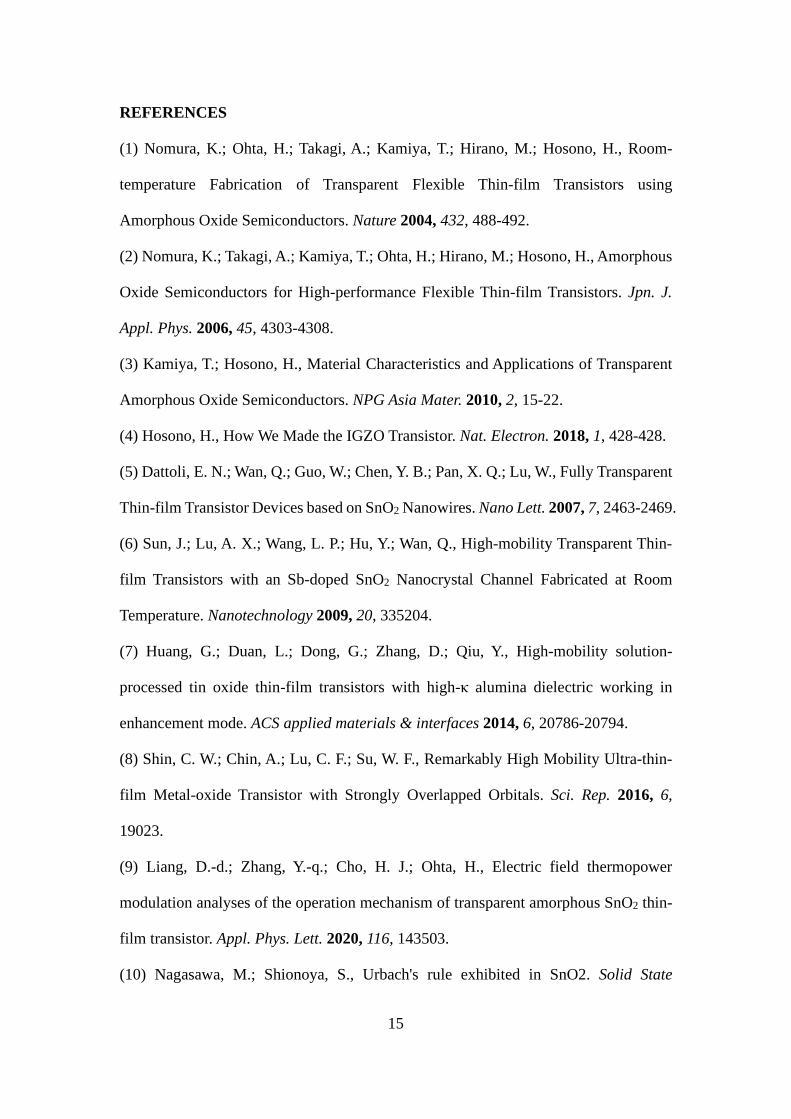
In order to address this issue, recently, we analyzed the effective channel thickness of
a-SnO2-based TTFT with the bottom-gate top-contact electrode configuration as
schematically shown in Fig. 1(a).9 We found that carrier electrons at ~2.5-nm-thick
SnO2 top surface were depleted due to gas (oxygen) adsorption and carrier electrons at
~1.7-nm-thick effective channel were modulated by the electric field application.
However, the thickness of SnO2 has not been optimized to obtain high performance
TTFTs showing large on-to-off current ratio and field effect mobility.
Here we show the optimization of SnO2 film thickness for TTFTs. We systematically
investigated the electron transport properties and the bandgap of SnO2 films with
various thicknesses. Then, we optimized the SnO2 thickness by analyzing the operation
mechanism of the TTFTs using electric field thermopower modulation technique. As a
4
result, TTFT based on the 4.2-nm-thick SnO2 film exhibited excellent characteristics;
highest on-to-off current ratio (~105) and high mobility (~20 cm2 V−1 s−1). The present
results would be essential to develop a-SnO2-based TTFTs in commercial applications.
RESULTS AND DISCUSSION
Optoelectronic Properties of SnO2 Films with Various Thicknesses
We fabricated SnO2 films with various thicknesses (3.2 – 41.6 nm) on SiO2 glass
substrates. The thicknesses were calculated from the Kiessig fringes measured by X-
ray reflectivity (XRR) [Fig. 2(a)]. Figure 2(b) shows the glancing angle (0.5°) incidence
X-ray diffraction (GIXRD) patterns of the SnO2 films. Intense diffraction peaks of rutile
structured SnO2 are seen in the GIXRD patterns of 41.6 and 32.5 nm films. The peaks
became broad and weak with decreasing thickness. When the thickness is thinner than
6 nm, diffraction peak disappeared, and halos were detected, indicating that the films
were amorphous. From the crystallite sizes [inset of Fig. 2(b)], which were calculated
from the diffraction peak width of 211 using Scherrer equation, we found that there is
a threshold thickness (~8 nm) separating amorphous and crystalline phases of SnO2.
Next, we investigated the optical band gap (Eg opt) of the SnO2 films [Figs. 3(a) and
3(b)], which was obtained from the x intercept of (αhν)2−hν plot (Tauc plot). In case of
5
17.4-nm-thick SnO2 film, the Eg opt was 3.60 eV [Fig. 3(a)], consistent with bulk SnO2.10
Figure 3(b) shows change in the Eg opt as a function of film thickness. The Eg opt
dramatically increases with decreasing thickness when the thickness is thinner than 10
nm, whereas thicker films (>18 nm) show bulk-like Eg opt. This is attributed to the
quantum size effect, which can be expressed as 11
Eg opt = 3.6 + h2/2L2(1/me + 1/mh)
where h is the Planck’s constant, me and mh are the effective masses of the electron and
hole in the semiconductor (me = 0.25 m012, mh = 0.47 m0
9 of SnO2), respectively, and L
is the thickness of the SnO2 thin films. The calculated Eg opt (solid line) clearly
reproduces the observed Eg opt (circles). This demonstrates that reducing the thickness
of amorphous SnO2 films results in a dramatic widening of the Eg opt due to the quantum
size effect.
Next, we investigated the electron transport properties of the SnO2 thin films at room
temperature (RT) [Figs 4(a)−4(d)]. It should be noted that the amorphous films showed
opposite tendencies to the polycrystalline films. The electrical resistivity (ρ) decreased
with decreasing thickness when the thickness is thicker than ~8 nm (polycrystalline),
whereas it increased with decreasing thickness when the thickness is thinner than ~8
nm (amorphous) [Fig. 4(a)]. These tendencies were supported by the Hall mobility

6
(μHall) [Fig. 4(b)], carrier concentration (n) [Fig. 4(c)], and thermopower (−S) [Fig. 4(d)].
The n tends to increase with decreasing the crystallite size [Fig. 4(c)]. Since SnO2 is an
n-type oxide semiconductor, the majority carrier is electron, which comes from the
nonstoichiometric SnO2−δ. In the case of polycrystalline, grain boundaries serve as
unintentional donor defects by annihilating or trapping charge carriers. Such examples
include for native donor defects such as oxygen vacancy, which tend to aggregate at
grain boundaries.13-14 Hence, as the grain boundary fraction increase, the n gradually
increases. However, when the thickness is thinner than ~8 nm, the conduction band
minimum (CBM) increases due to quantum size effect as explained previously [Fig.
3(b)]. Therefore, the n decreased with decreasing thickness in the amorphous phase. S
values reflect the tendency of n [Fig. 4(d)]. The μHall gradually increased with
decreasing thickness [Fig. 4(b)] and reached ~15 cm2 V−1 s−1 when the thickness was
~4 nm.
In order to clarify the thickness dependence of μHall, we measured ρ−T curves of the
SnO2 films from 300 to 30 K [Fig. 4(e)]. The ρ for the entire SnO2 films increased with
decreasing temperature, indicating a semiconducting behavior. We calculated the
activation energy of the electrical conductivity (Ea) using the Arrhenius plots as shown
in Fig. 4(f). In the polycrystalline region, the Ea increases with decreasing thickness,
7
most likely due to the reduction of boundary scattering of carrier electrons at grain
boundaries. In case of amorphous region, the Ea is small as compared to the
polycrystalline due to the absence of boundary scattering. The 3.2-nm-thick SnO2 film
showed larger Ea, most likely due to higher CBM energy. From these results, we
concluded that the a-SnO2 thin films with a thickness between 4−6 nm shows ideal
electron transport properties as the TFT channel.
Thickness Optimization of Amorphous SnO2 Film for Transistors
We fabricated several TTFTs using a-SnO2 films with various thicknesses (4.2 nm, 4.5
nm, 5.2 nm, and 6.2 nm). Figures 5(a)−5(d) show the transfer (Id−Vg) characteristics of
the a-SnO2 TTFTs. The on-to-off current ratio of the 6.2-nm-thick SnO2 TTFT was only
2.6, due to large sheet carrier concentration [ns = Ci·(Vg −Vth)⋅e−1 where Ci is the
capacitance per unit area (Ci ~110 nF cm−2)] (Fig. S2). The threshold gate voltage (Vth)
was −58.7 V (Fig. S1). The on-to-off current ratio and Vth increased with decreasing the
SnO2 film thickness. The 4.2-nm-thick SnO2 TTFT showed largest on-to-off current
ratio of ~105. The field effect mobility (µFE) (Fig. S3), calculated from µFE =
gm⋅[(W/L)⋅Ci·Vd]−1 (where gm is the transconductance ∂Id/∂Vg), was ~20 cm2 V−1 s−1 in
all a-SnO2 TTFTs.
8
Then, we measured the S during the transfer characteristics measurements (electric field
thermopower modulation). Figures 5(e)−5(f) show relationship between the −S and the
Vg. The S values were negative, indicating that the SnO2 film is n-type semiconductor.
The |S| decreases monotonically with Vg in all a-SnO2 TTFTs due to the increase in ns.
It should be noted that the absolute value of S increased with decreasing SnO2 thickness,
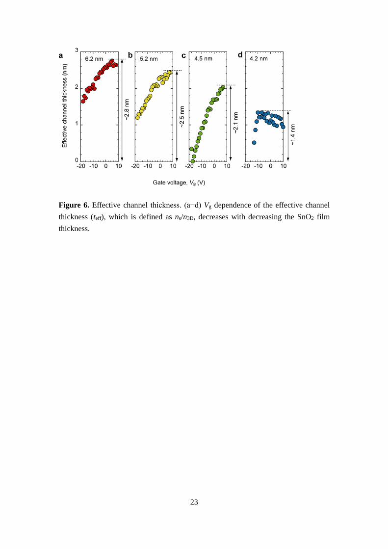
showing the reduction of ns. Since −S values reflect the volume carrier concentration,
we can estimate the effective electron channel thickness (teff) as teff ≡ ns/n3D, where n3D
is three-dimensional carrier concentration obtained from S−n3D relationship as shown
in Fig. S5.
Here we show the teff of the a-SnO2 TTFTs during Vg application [Figs. 6(a)−6(d)]. teff
gradually increased with Vg in all cases. The 6.2-nm-thick, 5.2-nm-thick, and 4.5-nm-
thick SnO2 TTFTs showed continuous increasing tendency of teff instead of reaching a
saturation. This behavior is due to the high ns along with the small regions of S
modulation. And the maximum teff decreases as the thickness of the a-SnO2 channel
decreases. On the other hand, the 4.2-nm-thick SnO2 TTFT showed clear saturation of
teff (~1.4 nm) when Vg > −6 V. In other words, the depletion layer thickness is ~2.8 nm
due to the oxygen adsorption, which agrees well with the previously reported depletion
layer thickness.9, 15 From these results, we concluded that the optimal thickness of a-
9
SnO2 is 4.2 nm for good TTFT showing rather large µFE (~20 cm2 V−1 s−1) and on-to-
off current ratio (~105).
We showed that the optimal thickness of a-SnO2 for TTFT is 4.2 nm in the case of
bottom-gate top-contact structure without a passivation layer. These results provide a
guideline for realizing practical a-SnO2 based TTFT. However, due to the strong gas-
sensitive characteristics of SnO2, the bottom-gate top-contact structure of the SnO2
TTFT is ambiently unstable. Hence, further improvement is required such as use of a
passivation layer on the top surface of SnO2 layer or change the structure of the bottom-
gate top-contact to enhance its ambient stability. We believe that the thickness of a-
SnO2 for TTFT with any gate structure can be optimized by analyzing the operation
mechanism of the TTFTs using electric field thermopower modulation.
CONCLUSION
In summary, we have shown the optimization of SnO2 film thickness for bottom-gate
TTFTs. We systematically investigated the electron transport properties and the
bandgap of SnO2 films with various thickness. When the film thickness is thinner than
8 nm, the film becomes amorphous. The optical bandgap, carrier concentration, and
Hall mobility of the 4-nm-thick amorphous SnO2 film were ~4.2 eV, 5 × 1019 cm−3, and
10
~15 cm2 V−1 s−1. Then, we optimized the SnO2 thickness by analyzing the operation
mechanism of the TTFTs using electric field thermopower modulation technique. As a
result, TTFT based on the 4.2-nm-thick SnO2 film exhibited excellent characteristics;
highest on-to-off current ratio (~105) and high mobility (~20 cm2 V−1 s−1). The present
results would be essential to develop a-SnO2-based TTFTs in commercial applications.
EXPERIMENTAL PROCEDURES
Fabrication and Analyses of the SnO2 thin films. SnO2 films with different
thicknesses were fabricated on SiO2 glass substrates by pulsed laser deposition (PLD)
technique (KrF excimer laser, λ = 248 nm, fluence ~0.3 J cm−2 pulse−1, repetition rate
= 5 Hz) at a substrate temperature of 300 °C. After the film growth, the films were
annealed at 400 °C for 30 min in air. The resultant films were analyzed by X-ray
diffraction (XRD, Cu Kα1, λ = 1.54059 Å, ATX-G, Rigaku Co.) measurements. Optical
transmission and reflection spectra of the resultant films were measured using an
ultraviolet-visible-near-infrared spectrometer (UV−vis−NIR, SolidSpec-3700,
Shimadzu Co.) at RT. Electrical resistivity (ρ), carrier concentration (n), and Hall
mobility (μHall) of the SnO2 thin films were measured by dc four-probe method with van
der Pauw electrode configuration. Thermopower (S) was measured at RT.

11
Fabrication of the TTFTs. The bottom-gate top-contact TTFTs were fabricated as
previous report.9 A 160-nm-thick polycrystalline HfO2 film, which was deposited at
room temperature, was used as the gate insulator film (the dielectric permittivity, εr =
21−2316).
Thermopower analyses of the TTFTs. S of the TTFT channel was measured by
conventional steady state method. Details of the electric field modulated S measurement
are described elsewhere.17-20
ASSOCIATED CONTENT
Supporting Information
Supporting Information is available free of charge via the Internet at
https://pubs.acs.org/doi/10.1021/acsaelm.xxxxxxx.
Id0.5−Vg curves of the bottom-gate top-contact a-SnO2 TTFTs; Changes in the sheet
carrier concentration (ns) as function of Vg; Changes in the field effect mobility (μFE) as
function of Vg; Optical absorption spectrum of the polycrystalline HfO2 thin film
deposited on SiO2 glass substrate; Three-dimensional carrier concentration (n3D)
dependence S of the SnO2 films.
12
AUTHOR INFORMATION
Corresponding Authors
Dou-dou Liang
The Beijing Municipal Key Laboratory of New Energy Materials and Technologies,
School of Materials Science and Engineering, University of Science and Technology
Beijing, Beijing 100083, China
ORCiD: orcid.org/0000-0002-4112-2069
Email: [email protected]
Hiromichi Ohta
Research Institute for Electronic Science, Hokkaido University, N20W10, Kita,
Sapporo 001-0020, Japan
ORCiD: orcid.org/0000-0001-7013-0343
Email: [email protected]
Authors
Binjie Chen

13
Graduate School of Information Science and Technology, Hokkaido University,
N14W9, Kita, Sapporo 060-0814, Japan
ORCiD: orcid.org/0000-0003-1838-2804
Hai Jun Cho
Research Institute for Electronic Science, Hokkaido University, N20W10, Kita,
Sapporo 001-0020, Japan
ORCiD: orcid.org/0000-0002-8642-4183
Complete contact information is available at:
https://pubs.acs.org/doi/10.1021/acsaelm.xxxxxxx.
Author Contributions
D.L. and B.C. performed the sample preparation and measurements. D.L. and H.O.
planned and supervised the project. All authors discussed the results and commented
on the manuscript.
Funding Sources

14
Dou-dou Liang received scholarship from the China Scholarship Council
(201806460051). Binjie Chen received scholarship from Japanese Government
(Monbukagakusho: MEXT) Scholarship (191555). Hai Jun Cho received funding from
Nippon Sheet Glass Foundation for Materials Science and Engineering. Hiromichi Ohta
received founding from Grants-in-Aid of the JSPS (19H05791 and 17H01314).
Notes
The authors declare no competing financial interest.
ACKNOWLEDGEMENTS
This research was supported by Grants-in-Aid for Innovative Areas (19H05791) and
Scientific Research A (17H01314) from the JSPS. D.L. greatly appreciates the support
from China Scholarship Council (201806460051). B.C. appreciates the support from
Japanese Government (Monbukagakusho: MEXT) Scholarship (191555). H.J.C.
acknowledges the support from Nippon Sheet Glass Foundation for Materials Science
and Engineering. A part of this work was also supported by Dynamic Alliance for Open
Innovation Bridging Human, Environment, and Materials, and by the Network Joint
Research Center for Materials and Devices.
15
REFERENCES
(1) Nomura, K.; Ohta, H.; Takagi, A.; Kamiya, T.; Hirano, M.; Hosono, H., Room-
temperature Fabrication of Transparent Flexible Thin-film Transistors using
Amorphous Oxide Semiconductors. Nature 2004, 432, 488-492.
(2) Nomura, K.; Takagi, A.; Kamiya, T.; Ohta, H.; Hirano, M.; Hosono, H., Amorphous
Oxide Semiconductors for High-performance Flexible Thin-film Transistors. Jpn. J.
Appl. Phys. 2006, 45, 4303-4308.
(3) Kamiya, T.; Hosono, H., Material Characteristics and Applications of Transparent
Amorphous Oxide Semiconductors. NPG Asia Mater. 2010, 2, 15-22.
(4) Hosono, H., How We Made the IGZO Transistor. Nat. Electron. 2018, 1, 428-428.
(5) Dattoli, E. N.; Wan, Q.; Guo, W.; Chen, Y. B.; Pan, X. Q.; Lu, W., Fully Transparent
Thin-film Transistor Devices based on SnO2 Nanowires. Nano Lett. 2007, 7, 2463-2469.
(6) Sun, J.; Lu, A. X.; Wang, L. P.; Hu, Y.; Wan, Q., High-mobility Transparent Thin-
film Transistors with an Sb-doped SnO2 Nanocrystal Channel Fabricated at Room
Temperature. Nanotechnology 2009, 20, 335204.
(7) Huang, G.; Duan, L.; Dong, G.; Zhang, D.; Qiu, Y., High-mobility solution-
processed tin oxide thin-film transistors with high-κ alumina dielectric working in
enhancement mode. ACS applied materials & interfaces 2014, 6, 20786-20794.
(8) Shin, C. W.; Chin, A.; Lu, C. F.; Su, W. F., Remarkably High Mobility Ultra-thin-
film Metal-oxide Transistor with Strongly Overlapped Orbitals. Sci. Rep. 2016, 6,
19023.
(9) Liang, D.-d.; Zhang, Y.-q.; Cho, H. J.; Ohta, H., Electric field thermopower
modulation analyses of the operation mechanism of transparent amorphous SnO2 thin-
film transistor. Appl. Phys. Lett. 2020, 116, 143503.
(10) Nagasawa, M.; Shionoya, S., Urbach's rule exhibited in SnO2. Solid State
16
Communications 1969, 7, 1731-1733.
(11) Lin, Y. H.; Faber, H.; Labram, J. G.; Stratakis, E.; Sygellou, L.; Kymakis, E.; Hastas,
N. A.; Li, R.; Zhao, K.; Amassian, A., High Electron mobility thin‐film transistors based
on solution‐processed semiconducting metal oxide heterojunctions and quasi‐
superlattices. Advanced Science 2015, 2, 1500058.
(12) Chen, R.; Wang, W.; Lu, M.; Chen, Y.; Lin, H.; Chen, K.; Chen, L., Anomalous
quantum efficiency for photoconduction and its power dependence in metal oxide
semiconductor nanowires. Nanoscale 2013, 5, 6867-6873.
(13) Sellers, M. C.; Seebauer, E. G., Manipulation of polycrystalline TiO2 carrier
concentration via electrically active native defects. Journal of Vacuum Science &
Technology A: Vacuum, Surfaces, and Films 2011, 29, 061503.
(14) Barlaz, D. E.; Seebauer, E. G., Manipulation of carrier concentration, crystallite
size and density in polycrystalline anatase TiO 2 via amorphous-phase medium range
atomic order. CrystEngComm 2015, 17, 2101-2109.
(15) Lantto, V.; Rantala, T. T.; Rantala, T. S., Atomistic Understanding of
Semiconductor Gas Sensors. J. Eur. Ceram. Soc. 2001, 21, 1961-1965.
(16) Lin, Y.-S.; Puthenkovilakam, R.; Chang, J., Dielectric property and thermal
stability of HfO 2 on silicon. Applied physics letters 2002, 81, 2041-2043.
(17) Ohta, H.; Masuoka, Y.; Asahi, R.; Kato, T.; Ikuhara, Y.; Nomura, K.; Hosono, H.,
Field-modulated Thermopower in SrTiO3-based Field-effect Transistors with
Amorphous 12CaO-7Al2O3 Glass Gate Insulator. Appl. Phys. Lett. 2009, 95, 113505.
(18) Ohta, H.; Mizuno, T.; Zheng, S. J.; Kato, T.; Ikuhara, Y.; Abe, K.; Kumomi, H.;
Nomura, K.; Hosono, H., Unusually Large Enhancement of Thermopower in an Electric
Field Induced Two-dimensional Electron Gas. Adv. Mater. 2012, 24, 740-744.
(19) Sanchela, A. V.; Onozato, T.; Feng, B.; Ikuhara, Y.; Ohta, H., Thermopower

17
modulation clarification of the intrinsic effective mass in transparent oxide
semiconductor BaSnO3. Phys. Rev. Materials 2017, 1, 034603.
(20) Sanchela, A. V.; Wei, M.; Cho, H. J.; Ohta, H., Thermopower Modulation
Clarification of the Operating Mechanism in Wide Bandgap BaSnO3-SrSnO3 Solid-
Solution Based Thin Film Transistors. Small 2019, 15, 1805394.
18
Figure 1. Concept of this research. (a) Schematic illustration of the electric filed thermopower modulation measurement of the bottom-gate top-contact a-SnO2 TTFT. (b) The energy band diagram around the conduction band of a-SnO2 TTFT. Raised questions are the best thickness of SnO2, on-to-off current ratio, field effect mobility, threshold voltage, and subthreshold swing.

19
Figure 2. X-ray analyses of the SnO2 thin films. (a) X-ray reflectivity of the SnO2 thin
films. The film thickness was calculated from the Kiessig fringes. (b) Glancing angle
(0.5°) incidence X-ray diffraction pattern. The inset shows the crystallite size of the
SnO2 thin films, which was calculated from the diffraction peak of 211 using the
Scherrer equation. When the thickness is thinner than 6 nm, the diffraction peak is not
seen, indicating amorphous.

20
Figure 3. Quantum size effect of the SnO2 thin films. (a) Tauc plot of the 17.4 nm-thick
SnO2 thin film deposited on SiO2 glass substrate. The optical bandgap is 3.6 eV. Inset
shows the transmission (T), reflection (R), and absorption (A) spectra. (b) Thickness
dependent optical bandgap (Eg opt). Dotted line shows bulk SnO2 (3.6 eV). The Eg opt
dramatically increases with decreasing thickness when the thickness is thinner than 10
nm, whereas thicker films (>18 nm) show bulk-like Eg opt. The solid lines illustrate the
calculated Eg opt for an infinite quantum well using Equation:
Eg opt=3.6+h2/2L2(1/me+1/mh).

21
Figure 4. Electron transport properties of the SnO2 thin films. Change in (a) resistivity (ρ), (b) Hall mobility (μHall), (c) carrier concentration (n), (d) thermopower (S) as a function of the thickness of SnO2 thin films. Note that the amorphous films showed opposite tendencies to the polycrystalline films. (e) Arrhenius plots of the ρ−T curves of the SnO2 films. (f) The activation energy of the electrical conductivity (Ea), which was calculated from Fig. 4(e).

22
Figure 5. Electric field thermopower modulation analyses of the bottom-gate top-contact a-SnO2 TTFTs. (a−d) Transfer (Id−Vg) characteristics at Vd = +0.1 V. Corresponding Ig−Vg curves are also shown (black square). The Ig is < 300 pA. (e−h) Electric field modulated thermopower (S) at various Vg ranging from −20 V to +8 V. The −S gradually decreases with Vg.
23
Figure 6. Effective channel thickness. (a−d) Vg dependence of the effective channel thickness (teff), which is defined as ns/n3D, decreases with decreasing the SnO2 film thickness.

24
Supporting Information
Thickness Optimization toward High-Performance Bottom-
Gated Transparent Tin Dioxide Thin-Film Transistor
Dou-dou Liang,*,1,2 Binjie Chen,3 Hai Jun Cho,2,3 and Hiromichi Ohta*,2,3
1The Beijing Municipal Key Laboratory of New Energy Materials and Technologies,
School of Materials Science and Engineering, University of Science and Technology
Beijing, Beijing 100083, China
2Research Institute for Electronic Science, Hokkaido University, N20W10, Kita,
Sapporo 001−0020, Japan
3Graduate School of Information Science and Technology, Hokkaido University,
N14W9, Kita, Sapporo 060−0814, Japan
*To whom correspondence should be addressed Email:

25
Figure S1. Id0.5−Vg curves of the bottom-gate top-contact a-SnO2 TTFTs. The threshold voltage (Vth) is gradually decreasing with increased SnO2 channel thickness.
26
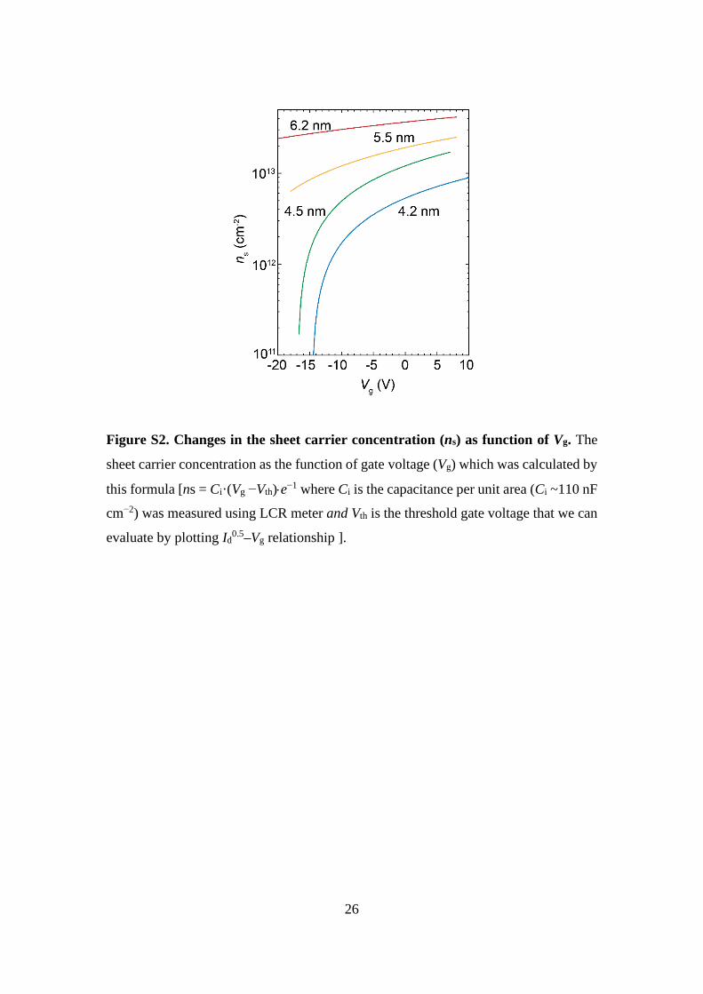
Figure S2. Changes in the sheet carrier concentration (ns) as function of Vg. The
sheet carrier concentration as the function of gate voltage (Vg) which was calculated by
this formula [ns = Ci·(Vg −Vth)⋅e−1 where Ci is the capacitance per unit area (Ci ~110 nF
cm−2) was measured using LCR meter and Vth is the threshold gate voltage that we can
evaluate by plotting Id0.5–Vg relationship ].

27
Figure S3. Changes in the field effect mobility (μFE) as function of Vg. The μFE
reaches ~20 cm2 V−1 s−1.

28
Figure S4. Optical absorption spectrum of the polycrystalline HfO2 thin film
deposited on SiO2 glass substrate. The optical bandgap is 5.8 eV. Inset shows
transmission (T) and reflection (R) spectra. Note the thickness of the HfO2 film was
63.4 nm and the HfO2 film was electrically insulator.

29
Figure S5. Three-dimensional carrier concentration (n3D) dependence S of the SnO2 films. The carrier effective mass (m*) of the SnO2 film around 0.47 me.