Thick CZT Detectors for Space-Borne X-ray Astronomy · Thick CZT Detectors for Space-Borne X-ray...
13
Thick CZT Detectors for Space-Borne X-ray Astronomy H. Krawczynski a , I. Jung a , J. Perkins a , A. Burger b , M. Groza b a Washington University in St. Louis, Department of Physics, 1 Brookings Dr., CB 1105, St. Louis, MO 63130; b Fisk University, Department of Physics, 1000 Seventeenth Ave. North, Nashville, TN 37208 ABSTRACT Cadmium Zinc Telluride (CZT) detectors are having a major impact on the field of hard X-ray astronomy. Without the need for cryogenic cooling they achieve good spatial and energy resolutions over the broad energy range from 10 keV to ∼600 keV. In this paper, we briefly review the historical development of detectors used in X- ray astronomy. Subsequently, we present an evaluation of CZT detectors from the company Imarad. The standard 2×2×0.5 cm detectors, contacted with 8×8 In pixels and an In cathode, exhibit FWHM energy resolutions of 7 keV at 59 keV, and 10 keV at 662 keV. A direct measurement of the 662 keV photopeak efficiency gives 67%. We have started a detailed study of the performance of Imarad detectors depending on surface preparation, contact materials, contact deposition, post-deposition detector annealing, and detector passivation techniques. We present first results from contacting detectors with Cr, Ag, Au, and Pt. Keywords: C ZT, X-ray and Gamma-ray detectors, space-applications, contact technology. 1. INTRODUCTION – DETECTORS IN X-RAY ASTRONOMY X-ray astronomy has come a long way since the first detection of X-ray emission from an extra-solar object in 1962. 1 In the meantime, X-ray astronomy has emerged as one of the drivers of modern astronomy, as evident from the award of the Nobel prize in physics to X-ray pioneer Riccardo Giacconi in 2002, and the existence of two major X-ray observatories, Chandra and XMM-Newton, orbiting Earth since 1999. The most important results of X-ray astronomy have so far been obtained from observations in the “soft” X-ray band with photon energies between 0.1 keV and several keV. To mention several important milestones, the Einstein observatory 2 achieved in 1978 a first breakthrough in the 0.2 keV to 4 keV band by combining a grazing incidence mirror with position sensitive detectors. The observatory carried a “High Resolution Imager” (HRI), consisting of two cascaded Micro Channel Plates (MCP) read out by a crossed-grid charge detector. Another main instrument was the Imaging Proportional Counter (IPC), a 4 cm deep, 800 Torr Ar-Xe-CO 2 proportional counter which achieved a modest energy resolution of between 50% and 100%. The grazing incidence mirror and the HRI achieved an effective detection area of 10 cm 2 . The mirror and the IPC had a detection area of 100 cm 2 . The Roentgen Satellite (ROSAT) was launched in 1990 and used similar detectors as the Einstein observatory. Its HRI and IPC cameras collected respectively 8 and 2.4 times more photons per unit time than their Einstein counterparts. 3 The Chandra and XMM-Newton satellites are equipped with powerful X-ray grazing incidence mirrors and state-of-the-art photon detectors. The Chandra satellite carries the Advanced CCD imaging spectrometer (ACIS) 4 made of Si-CCDs with energy resolutions of between 2% and 10% over the energy range from 0.1 keV to 10 keV. The XMM-Newton satellite carries two conventional Metal Oxide Semiconductor (MOS) cameras, and a “PN” camera. 5 The fully depleted pn CCDs (280 micron deep depletion region) can detect X-rays with energies up to 15 keV. The Chandra X-ray mirror and ACIS camera achieve a 1 keV detection area of 340 cm 2 and an unique angular resolution of 0.5”. The XMM-Newton mirrors and CCD cameras have a combined 1 keV detection area of 2,100 cm 2 and an angular resolution of 15”. Compared to the soft X-ray band, the hard X-ray band (∼ 20-200 keV) has progressed more slowly. Hard X-rays are more difficult to focus, scintillation detectors had only modest spatial and energy resolutions, and Ge Further author information: Send correspondence to H.K.: E-mail: [email protected], Telephone: 314 935 8553
Transcript of Thick CZT Detectors for Space-Borne X-ray Astronomy · Thick CZT Detectors for Space-Borne X-ray...
Thick CZT Detectors for Space-Borne X-ray Astronomy
H. Krawczynskia, I. Junga, J. Perkinsa, A. Burgerb, M. Grozab
aWashington University in St. Louis, Department of Physics,
1 Brookings Dr., CB 1105, St. Louis, MO 63130;
bFisk University, Department of Physics,
1000 Seventeenth Ave. North, Nashville, TN 37208
ABSTRACT
Cadmium Zinc Telluride (CZT) detectors are having a major impact on the field of hard X-ray astronomy.Without the need for cryogenic cooling they achieve good spatial and energy resolutions over the broad energyrange from 10 keV to ∼600 keV. In this paper, we briefly review the historical development of detectors used in X-ray astronomy. Subsequently, we present an evaluation of CZT detectors from the company Imarad. The standard2×2×0.5 cm detectors, contacted with 8×8 In pixels and an In cathode, exhibit FWHM energy resolutions of 7keV at 59 keV, and 10 keV at 662 keV. A direct measurement of the 662 keV photopeak efficiency gives 67%.We have started a detailed study of the performance of Imarad detectors depending on surface preparation,contact materials, contact deposition, post-deposition detector annealing, and detector passivation techniques.We present first results from contacting detectors with Cr, Ag, Au, and Pt.
Keywords: C ZT, X-ray and Gamma-ray detectors, space-applications, contact technology.
1. INTRODUCTION – DETECTORS IN X-RAY ASTRONOMY
X-ray astronomy has come a long way since the first detection of X-ray emission from an extra-solar object in1962.1 In the meantime, X-ray astronomy has emerged as one of the drivers of modern astronomy, as evidentfrom the award of the Nobel prize in physics to X-ray pioneer Riccardo Giacconi in 2002, and the existence oftwo major X-ray observatories, Chandra and XMM-Newton, orbiting Earth since 1999.
The most important results of X-ray astronomy have so far been obtained from observations in the “soft”X-ray band with photon energies between 0.1 keV and several keV. To mention several important milestones, theEinstein observatory2 achieved in 1978 a first breakthrough in the 0.2 keV to 4 keV band by combining a grazingincidence mirror with position sensitive detectors. The observatory carried a “High Resolution Imager” (HRI),consisting of two cascaded Micro Channel Plates (MCP) read out by a crossed-grid charge detector. Anothermain instrument was the Imaging Proportional Counter (IPC), a 4 cm deep, 800 Torr Ar-Xe-CO2 proportionalcounter which achieved a modest energy resolution of between 50% and 100%. The grazing incidence mirrorand the HRI achieved an effective detection area of 10 cm2. The mirror and the IPC had a detection area of100 cm2. The Roentgen Satellite (ROSAT) was launched in 1990 and used similar detectors as the Einsteinobservatory. Its HRI and IPC cameras collected respectively 8 and 2.4 times more photons per unit time thantheir Einstein counterparts.3 The Chandra and XMM-Newton satellites are equipped with powerful X-raygrazing incidence mirrors and state-of-the-art photon detectors. The Chandra satellite carries the AdvancedCCD imaging spectrometer (ACIS)4 made of Si-CCDs with energy resolutions of between 2% and 10% overthe energy range from 0.1 keV to 10 keV. The XMM-Newton satellite carries two conventional Metal OxideSemiconductor (MOS) cameras, and a “PN” camera.5 The fully depleted pn CCDs (280 micron deep depletionregion) can detect X-rays with energies up to 15 keV. The Chandra X-ray mirror and ACIS camera achieve a 1keV detection area of 340 cm2 and an unique angular resolution of 0.5”. The XMM-Newton mirrors and CCDcameras have a combined 1 keV detection area of 2,100 cm2 and an angular resolution of 15”.
Compared to the soft X-ray band, the hard X-ray band (∼ 20-200 keV) has progressed more slowly. HardX-rays are more difficult to focus, scintillation detectors had only modest spatial and energy resolutions, and Ge
Further author information: Send correspondence to H.K.: E-mail: [email protected], Telephone: 314 9358553
detectors required resource intensive cryogenic cooling. The High Energy Astrophysics Observatory-1 (HEAO-1)was equipped with a 1.4 × 20 fan collimator and 250 cm2 of NaI scintillator, and scanned the hard X-ray sky inthe years 1977-1979.6 More recently, the Rossi X-Ray Timing Explorer (RXTE)7 launched in 1995 and Satelliteper Astronomia X, “Beppo” (BeppoSAX)8 launched in 1996 used essentially the same detector technology with1 pencil beam collimators. The wide bandgap semiconductors Cadmium Telluride (CdTe) and Cadmium ZincTelluride (CZT) are now boosting the field of hard X-ray astronomy. The International Gamma-Ray AstrophysicsLaboratory (INTEGRAL)9 launched in 2002 carries the Imager on Board the Integral Satellite (IBIS) that usesCdTe detectors with a detector area of ∼2,600 cm2. The SWIFT satellite,10 to be launched in October 2004,carries the Burst Alert Telescope (BAT) with a CZT detection area of ∼5,240 cm2. The IBIS and the BAT usethe approach of coded mask imaging. Embedded in a collimator assembly, the detectors see the sky through apatterned shadow mask. The detectors image the sum of all shadows cast by the X-ray sources in the field ofview. A deconvolution algorithm is used to derive the X-ray surface brightness distribution from the detectedimage. In this approach, the effective detection area is roughly half of the active detector area (the other half ofthe detector area is covered by the coded mask), and is not given by the collection area of any focusing optics.
The congressionally approved Beyond Einstein Program11 of NASA’s “Structure and Evolution of the Uni-verse” theme plans for two major X-ray missions. In both missions, CZT plays an important role. TheConstellation-X observatory12 will perform high throughput X-ray spectroscopy with high energy and angu-lar resolution over the energy range from 0.25 keV to 10 keV employing X-ray gratings with Si-CCDs, as wellas non-dispersive microcalorimeters. The design includes a hard X-ray telescope that uses CZT detectors tocover the energy range from 6 keV to 40 keV or higher. Constellation-X is currently receiving NASA fundsfor Pre-Phase A development, the “advanced concepts” phase. Given the current budget plan, the mission willbe launched in 2016.13 A second recommended mission is the “black hole finder probe”, a large field of view,hard X-ray telescope. The Energetic X-ray Imaging Survey Telescope (EXIST) design14 proposes an assembly ofcoded mask imagers. Hard X-rays are detected with ∼0.5 cm thick CZT detectors with a total detector area of∼80,000 cm2. EXIST has been selected for a 2-year NASA concept study, along with the Coded Aperture SurveyTelescope for Energetic Radiation (CASTER),15 a competitor design which employs the new scintillators LaBr3or LaCl3 as primary detectors. There is no definitive time schedule for the black hole finder probe, as its fundingis presently beyond the budgetary horizon of 2009.13
In this paper, we emphasize thick CZT detectors and their application in EXIST-type hard X-ray telescopes.In Sect. 2 we will discuss key requirements for CZT detectors in this application. In Sect. 3 we scrutinizethe performance of In contacted standard detectors from Imarad. Furthermore, we present detailed detectorsimulations and compare simulated data with experimentally measured data. In Sect. 4 we give first results ofcontacting the detectors with Cr, Ag, Au, and Pt. Finally, in Sect. 5, we summarize our findings and describework in progress.
2. THICK CZT FOR HARD X-RAY TELESCOPES
2.1. CZT substrates
Presently, major vendors of CZT substrates are eV Products,16 Imarad,17 and Bicron.18 eV Products andBicron use the High-Pressure Bridgman (HPB) process to grow the substrates, while Imarad uses the modifiedHigh-Pressure Bridgman (mHPB) process. HPB substrates are more expensive than mHPB substrates, typicalprices for individual crystals being $2000 cm−3 and $350 cm−3, respectively. While HPB and mHPB CZT achievesimilar performances at high energies, mHPB detectors give poorer results at low energies. The latter can in partbe explained by the higher resistivity of HPB crystals (∼2·1011 ohm-cm) compared to mHPB crystals (∼1010
ohm-cm) that results in lower leakage currents. An alternative to CZT might be CdTe.19 An advantage of CdTeis that large uniform single crystals can be grown. Although CdTe detectors require cooling to temperatures of-20C to achieve good performances, such temperatures can easily be maintained in space.
2.2. Requirements for thick CZT detector in space-borne X-ray telescopes
In the following, we discuss the requirements for 0.5 cm thick CZT detectors used for the detection of 10 keV to600 keV photons in space-borne X-rays telescopes.
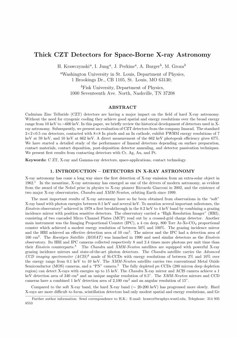
4 ChannelFast Amplification
BatteriesHigh Voltage
CZT DetectorWater Cooling
16 Channel ASIC
Test−In
Figure 1. Test set-up for evaluation of the CZT detector performance (Washington University). The hybrid read-outsystem consists of a low-noise ASIC readout for 16 pixels and a fast (100 MHz analog bandwidth) readout for 3 pixelsand the cathode; pixels which are not read out are held at ground potential.
Photopeak efficiency: A crucial detector parameter is the photopeak efficiency ε. The detector area required toachieve a certain flux sensitivity scales with 1/ε; the mass and cost of the full satellite can depend even morestrongly on ε. Even in a fully depleted detector and after full Depth of Interaction (DOI) correction, not allphoto-effect events show up in the measured energy spectra. The main culprit is most probably “dead detectorregions”. Owing to non-negligible surface conductivity, not all electric field lines end at the anode pixels: someend in-between pixels.20 Electron clouds drifting to the area between pixels induce less charge on the anodecontacts than clouds drifting to the anode contacts themselves. While large pixels minimize the dead volume,they usually do not give ideal energy resolutions. The volume of the dead regions can be reduced by passivatingthe detectors after contact deposition. Another approach is to use negatively biased steering contacts locatedbetween the anode contacts to steer the electrons toward the anode contacts.
Energy and spatial resolutions: The best reported energy resolutions of 0.5 mm thick CZT detectors are about 3keV at 59 keV and 7 keV at 662 keV.21–23 The EXIST design foresees pixellated detectors with a pixel pitch ofabout 1.25 mm to achieve an angular resolution of between 2’ and 5’. Pixellated detectors are preferred, as theyexhibit lower lead capacitance and lower leakage currents than strip detectors. DOI resolution of 1% or betteris required to assure that the anode signals can be corrected for any existing DOI dependence. An importantfact to notice is that energy resolutions below ∼100 keV are typically dominated by electronic noise (producedby the detector itself) and readout noise. The energy resolutions above ∼ 100 keV are dominated by crystalinhomogeneities and the dependence of the induced charge on the location of the photon absorption. Thus, adetector performing well at low energies does not necessarily perform well at high energies and vice versa. Whilepresent CZT technology gives high-energy resolutions that are sufficient for most astrophysical applications, asubstantial improvement of the low-energy resolution would be very welcomed.
Temperature range and mechanical ruggedness: In space, CZT detectors can conveniently be operated at temper-atures between -50C and 0C. Most CZT detectors show better performance at such low temperatures than atroom temperatures. However, some Imarad mHPB detectors equipped with blocking contacts basically stoppedworking at temperatures of about -10C.24 The detectors should also be rugged enough to withstand vibrationsduring the launch of the spacecraft.
Radiation hardness: Space-borne detectors suffer year long exposures to trapped charged particles, cosmic rays,and neutrons that damage the detectors and make them radioactive. Several groups have studied the radiationdamage of CZT detectors produced by high energy protons.25–29, 32 A 200 MeV proton dose of ∼109 cm−2
decreases the electron µ− τ product by 20% to 40% and reduces the charge yield by 10% to 20%.26, 29 Wong et
al. (1996)26 reported that annealing the detectors to about 100C can be used to undo the damage. Fraboni etal. (2003)33 irradiated CZT detectors with large doses of γ-rays, electrons (9 MeV), thermal (∼1 eV) and fast(∼1 MeV) neutrons, and protons (2 MeV). Using photo induced current transient spectroscopy they find thatthe degradation of the detector performance (increase in leakage current, loss of energy resolution, and shift ofthe photopeak to lower energies) is linked to the appearance of very specific deep energy levels.
Activation: Substrate activation is a serious concern for thick detectors. A number of background measurementshave been made in several balloon flights.29–31 Slavis et al. (2000)29 monitored the background during a 21 hrslong 104,000 ft high balloon flight and used the data to derive upper limits on the activation of a CZT detector.Murakami et al. (2003)32 activated a CdTe detector with 155 MeV protons and subsequently identified a largenumber of radio-active elements with a Ge detector and the CdTe detector itself. Although several Monte Carlostudies of CZT activation on different time scales have been published,34–37 there are no long-term activationdata to test the simulations. The INTEGRAL and SWIFT missions will provide data sets to improve on thissituation.
3. PERFORMANCE OF STANDARD IMARAD DETECTORS
In this section, we discuss the performance of standard Imarad detectors. The 2×2×0.5 cm detectors arecontacted with 8 × 8 In pixels on the anode side and a monolithic In cathode. The pixels have a diameter of1.6 mm and the pixel pitch is 2.4 mm. The detectors have a conducting band around their perimeter. Even whenleft floating, the band improves the photopeak efficiency and energy resolution of the outer pixels. We concentrateon the performance of central pixels. Previous measurements of Imarad detectors have been described by Naritaet al. (1999, 2000),22, 24 Li et al. (2001),38 Nemirovski et al. (2001),39 Hong et al. (2002),40 and Perkins et al.(2003).23
3.1. Mounting and electronic readout
We mount the detectors using gold plated pogo-pin contacts on both, the anode and the cathode sides. Thecathode is negatively biased, and the anode pixels are held at ground. We use a hybrid electronic readout (seeFig. 1). Four channels (3 anode pixels plus the cathode) are AC coupled and are amplified by a fast Amptek 250amplifier followed by a second amplifier stage. The amplified signals are digitized by a 500 MHz oscilloscope andtransferred to a PC via Ethernet. The time resolved readout enables us to measure the drift time of electronsthrough the detector to a resolution of 10 ns. We use a 16 channel ASIC from eV products16 to measure pulseheight information for 16 additional pixels. The ASIC gives amplified and shaped signals which we digitize withcustom designed VME boards. The FWHM noise of both readout chains lies between 5 keV and 10 keV. If notstated otherwise, we quote all energy resolutions after quadratic subtraction of the readout noise determined atzero detector bias.
3.2. Individual pulses
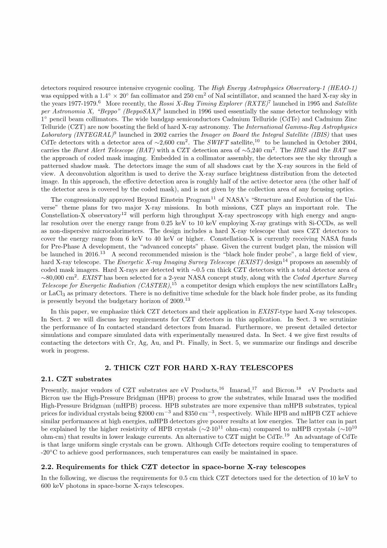
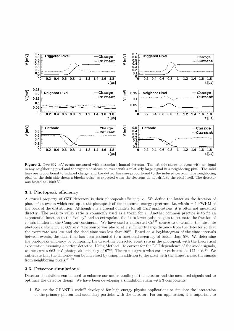
Figure 2 shows pulses induced by a 662 keV (Cs137) photon at a detector bias of -400 V. The time derivativeof the charge sensitive preamplifier shows the induced current. The current rises slowly as the electrons drifttoward the anode pixel. At the end of the 0.5 µsec pulse, a pronounced current peak can be recognized. Thepeak is caused by the rapidly decreasing weighting potential near the pixels owing to the small pixel effect.41, 42
Electron trapping is seen in an exponential decrease of the cathode current.
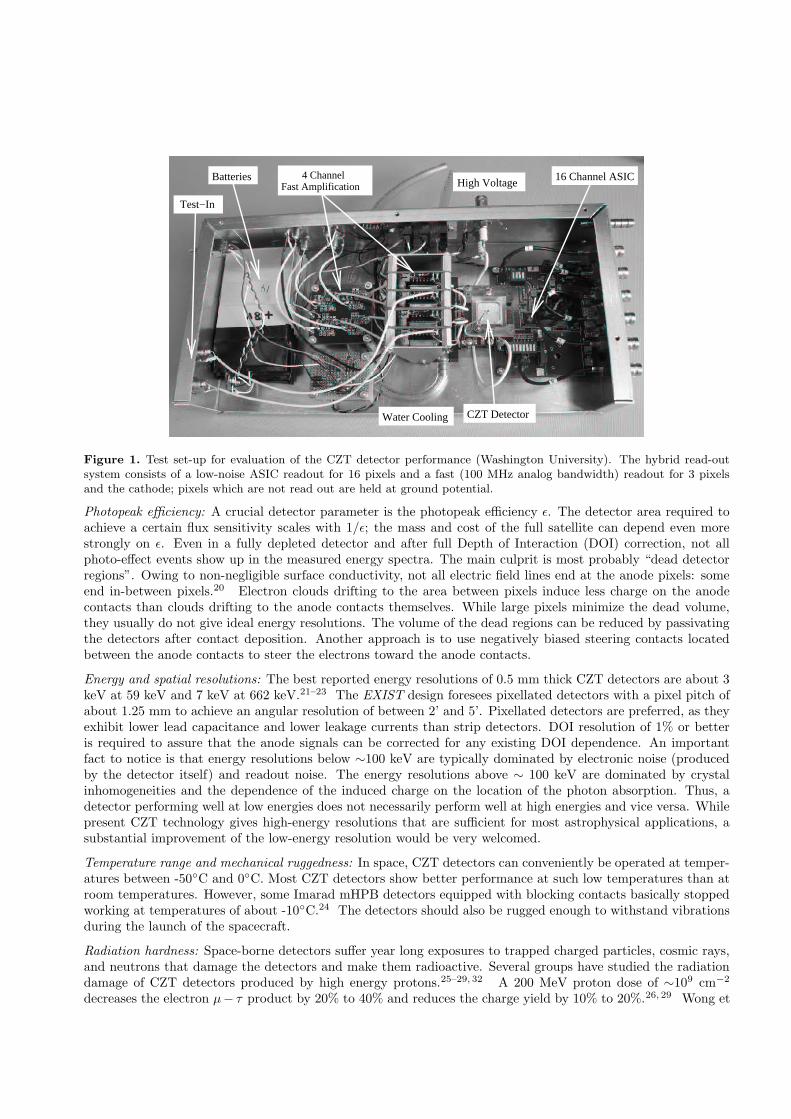
Figure 3 shows two events induced by 662 keV photons at a detector bias of -1000 V. The event on the leftside has no signal in any neighboring pixel, while the event on the right side has a neighboring pixel with arelatively large signal. The triggered pixel shows a large unipolar pulse for both events. In the second event, theadjacent pixel shows a bipolar pulse, as expected when the electrons do not drift to that pixel. We are currentlystudying the possibility to use the information encoded in bipolar pulses to improve the photopeak efficiencyand energy resolution of the detectors.

V (5 mV)I (a.u.)
V [
5 m
V ]
t [ µs ]
-50
0
50
100
-100
-50
0
50
0 1 2 3
Small PixelEffect
ElectricField
ElectronTrapping
Cathode
Anode
Figure 2. The panels show an anode (top) andcathode (bottom) pulse of a 662 keV photon mea-sured with a standard Imarad detector. In bothpanels, the solid line is proportional to the chargeinduced on the contact while the dashed line is thetime derivative of that charge. The vertical linesmark the beginning and end of the pulse. The an-ode current peaks toward the end of the pulse ow-ing to the small pixel effect. The cathode currentdecreases with time, probably owing to electrontrapping. The detector was biased at -400 V.
3.3. Energy spectra
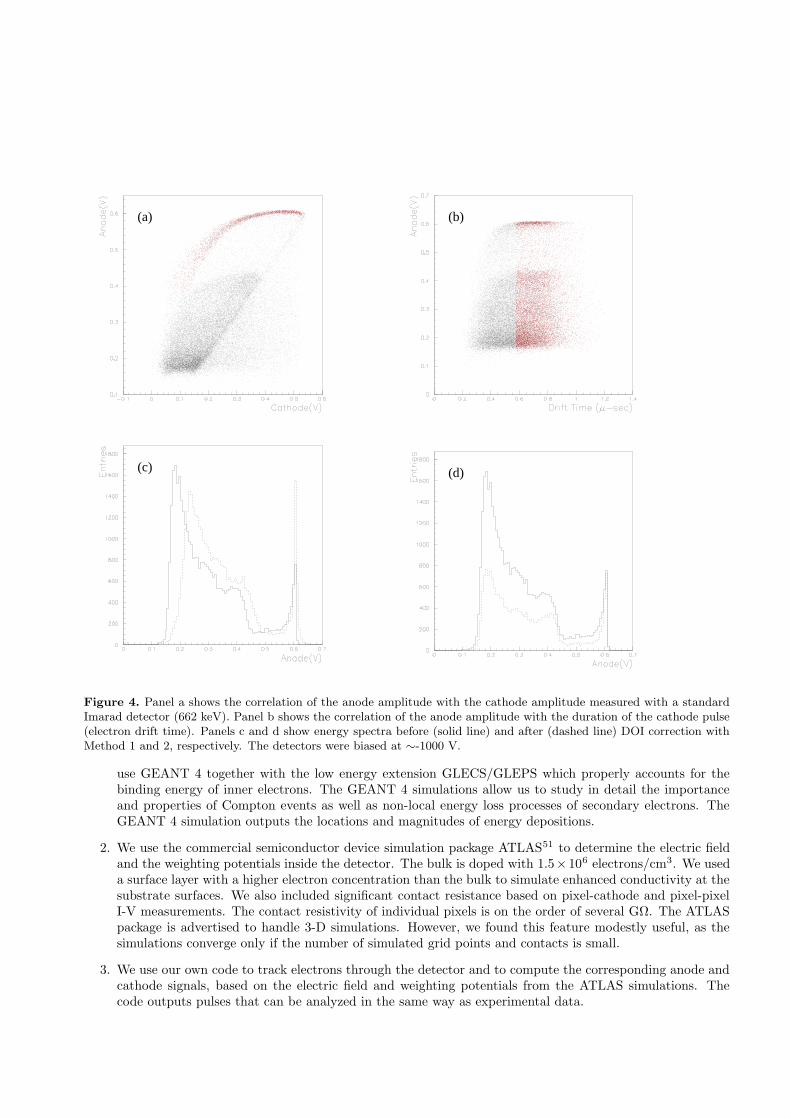
Owing to hole trapping, the induced anode signals depend on the DOI of the photon. The effect is mitigatedby the small pixel design of the detector. While the effect is negligible at energies below ∼100 keV (when allphotons interact close to the cathode), it becomes increasingly important at higher energies when the photonsstart penetrating the substrate. We compared two different methods to correct the anode signals for their DOIdependence (Fig. 4). Method 1 uses the correlation of the anode and cathode amplitudes (panel a). Method2 uses the correlation of the anode amplitude and the electron drift time as estimated from the length of thecathode pulse (panel b). Method 1 improves the photopeak efficiency by 57% and the FWHM energy resolutionfrom 11 keV to 10 keV (panel c). Method 2 does not work as well as Method 1. A cut in drift times tdrift >0.57 µsec does improve the energy resolution from 11 keV to 10 keV, but decreases the photopeak efficiency by14% (panel d).
At 59 keV, no DOI correction is needed as all photons interact near the cathode. We measured a 59 keVenergy resolution of 7 keV. Remarkably, the absolute resolutions at 59 keV and 662 keV are rather similar (7 keVand 10 keV, respectively). The result indicates that the resolution is dominated by electronic noise (producedby the detector) rather than by detector inhomogeneities. At -1000 V bias, we find typical leakage currents Id
between 7 nA and 14 nA. The associated shot noise43 is:
FWHMsh = 2.35 ωe√π
√
Id τsq
(1)
≈ 4.1 keV
(
Id10 nA
τs1µsec
)1/2
(2)
where ω ≈ 4.5 eV is the mean energy required to create an electron hole pair in CZT, e = 2.718, q is the electroncharge in Coulombs, and τs is the time constant of the shaping amplifier in seconds. The expression holds fora single stage CR-RC filter. A higher order filter (as used by us) reduces the noise by a factor of ∼ 1/1.5. Weconclude that shot noise associated with the leakage current does not dominate the 59 keV energy resolution of thedetectors. Although the electronic noise of CZT detectors has been discussed in the literature,39, 43–45 additionalwork is required to identify the dominant noise source for the special case of pixellated Imarad detectors.
s]µt [0 0.2 0.4 0.6 0.8 1 1.2 1.4 1.6 1.8
V [
mV
]
00.10.20.30.40.50.60.7 Triggered Pixel Charge
Current
s]µt [0 0.2 0.4 0.6 0.8 1 1.2 1.4 1.6 1.8
V [
mV
]
00.10.20.30.40.50.60.7 Triggered Pixel Charge
Current
s]µt [0 0.2 0.4 0.6 0.8 1 1.2 1.4 1.6 1.8
V [
mV
]
00.05
0.10.15
0.20.25
Neighbor Pixel ChargeCurrent
s]µt [0 0.2 0.4 0.6 0.8 1 1.2 1.4 1.6 1.8
V [
mV
]
0
0.05
0.1
0.15 Neighbor Pixel ChargeCurrent
s]µt [0 0.2 0.4 0.6 0.8 1 1.2 1.4 1.6 1.8
V [
mV
]
00.20.40.60.8
1 Cathode ChargeCurrent
s]µt [0 0.2 0.4 0.6 0.8 1 1.2 1.4 1.6 1.8
V [
mV
]
-0.10
0.10.20.30.40.5 Cathode Charge
Current
Figure 3. Two 662 keV events measured with a standard Imarad detector. The left side shows an event with no signalin any neighboring pixel and the right side shows an event with a relatively large signal in a neighboring pixel. The solidlines are proportional to induced charge, and the dotted lines are proportional to the induced current. The neighboringpixel on the right side shows a bipolar pulse, as expected when the electrons do not drift to the pixel itself. The detectorwas biased at -1000 V.
3.4. Photopeak efficiency
A crucial property of CZT detectors is their photopeak efficiency ε. We define the latter as the fraction ofphotoeffect events which end up in the photopeak of the measured energy spectrum, i.e. within ± 1 FWHM ofthe peak of the distribution. Although ε is a crucial quantity for all CZT applications, it is often not measureddirectly. The peak to valley ratio is commonly used as a token for ε. Another common practice is to fit anexponential function to the “valley” and to extrapolate the fit to lower pulse heights to estimate the fraction ofcounts hidden in the Compton continuum. We have used a calibrated Cs137 source to determine the absolutephotopeak efficiency at 662 keV. The source was placed at a sufficiently large distance from the detector so thatthe event rate was low and the dead time was less than 20%. Based on a log-histogram of the time intervalsbetween events, the dead-time has been estimated to a fractional accuracy of better than 5%. We determinethe photopeak efficiency by comparing the dead-time corrected event rate in the photopeak with the theoreticalexpectation assuming a perfect detector. Using Method 1 to correct for the DOI dependence of the anode signals,we measure a 662 keV photopeak efficiency of 67%. The result agrees with earlier estimates at 122 keV.24 Weanticipate that the efficiency can be increased by using, in addition to the pixel with the largest pulse, the signalsfrom neighboring pixels.46–49
3.5. Detector simulations
Detector simulations can be used to enhance our understanding of the detector and the measured signals and tooptimize the detector design. We have been developing a simulation chain with 3 components:
1. We use the GEANT 4 code50 developed for high energy physics applications to simulate the interactionof the primary photon and secondary particles with the detector. For our application, it is important to
(a) (b)
(c) (d)
Figure 4. Panel a shows the correlation of the anode amplitude with the cathode amplitude measured with a standardImarad detector (662 keV). Panel b shows the correlation of the anode amplitude with the duration of the cathode pulse(electron drift time). Panels c and d show energy spectra before (solid line) and after (dashed line) DOI correction withMethod 1 and 2, respectively. The detectors were biased at ∼-1000 V.
use GEANT 4 together with the low energy extension GLECS/GLEPS which properly accounts for thebinding energy of inner electrons. The GEANT 4 simulations allow us to study in detail the importanceand properties of Compton events as well as non-local energy loss processes of secondary electrons. TheGEANT 4 simulation outputs the locations and magnitudes of energy depositions.
2. We use the commercial semiconductor device simulation package ATLAS51 to determine the electric fieldand the weighting potentials inside the detector. The bulk is doped with 1.5×10⁶ electrons/cm3. We useda surface layer with a higher electron concentration than the bulk to simulate enhanced conductivity at thesubstrate surfaces. We also included significant contact resistance based on pixel-cathode and pixel-pixelI-V measurements. The contact resistivity of individual pixels is on the order of several GΩ. The ATLASpackage is advertised to handle 3-D simulations. However, we found this feature modestly useful, as thesimulations converge only if the number of simulated grid points and contacts is small.
3. We use our own code to track electrons through the detector and to compute the corresponding anode andcathode signals, based on the electric field and weighting potentials from the ATLAS simulations. Thecode outputs pulses that can be analyzed in the same way as experimental data.
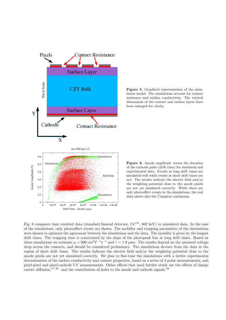
Figure 5. Graphical representation of the simu-lation model. The simulations account for contactresistance and surface conductivity. The verticaldimensions of the contact and surface layers havebeen enlarged for clarity.
0
0.1
0.2
0.3
0.4
0.5
0.6
0 2e-07 4e-07 6e-07 8e-07 1e-06 1.2e-06 1.4e-06
Ano
de A
mpl
itud
e (V
)
Drift Time - Anode (MicroSec)
mu=900 tau=1.5
Simulations
Simulations
Simulations
Real Data
(sec)
Figure 6. Anode amplitude versus the durationof the cathode pulse (drift time) for simulated andexperimental data. Events at long drift times aresimulated well while events at short drift times arenot. The results indicate the electric field and/orthe weighting potential close to the anode pixelsare not yet simulated correctly. While there areonly photoeffect events in the simulations, the realdata shows also the Compton continuum.
Fig. 6 compares time resolved data (standard Imarad detector, Cs137, 662 keV) to simulated data. In the caseof the simulations, only photoeffect events are shown. The mobility and trapping parameters of the simulationswere chosen to optimize the agreement between the simulations and the data. The mobility is given by the longestdrift times. The trapping time is constrained by the slope of the photopeak line at long drift times. Based onthese simulations we estimate µ = 900 cm2V−1s−1 and τ = 1.9 µsec. The results depend on the assumed voltagedrop across the contacts, and should be considered preliminary. The simulations deviate from the data in theregion of short drift times. The results indicate the electric field and/or the weighting potential close to theanode pixels are not yet simulated correctly. We plan to fine-tune the simulations with a better experimentaldetermination of the surface conductivity and contact properties, based on a series of 4 point measurements, andpixel-pixel and pixel-cathode I-V measurements. Other effects that need further study are the effects of chargecarrier diffusion,47, 49 and the contribution of holes to the anode and cathode signals.39
[V]
0 0.1 0.2 0.3 0.4 0.5 0.6 0.7
[No
rm. E
ntr
ies]
0
0.002
0.004
0.006
0.008
0.01
0.012
0.014
0.016
0.018
0.02
0.022
(662 keV)In
[V]
0 0.1 0.2 0.3 0.4 0.5 0.6 0.7
[No
rm. E
ntr
ies]
0
0.002
0.004
0.006
0.008
0.01
0.012
0.014
0.016
0.018
0.02
(662 keV)Cr
[V]
0 0.1 0.2 0.3 0.4 0.5 0.6 0.7
[No
rm. E
ntr
ies]
0
0.002
0.004
0.006
0.008
0.01
0.012
0.014
0.016
0.018
0.02
(662 keV)Ag
[V]
0 0.1 0.2 0.3 0.4 0.5 0.6 0.7
[No
rm. E
ntr
ies]
0
0.002
0.004
0.006
0.008
0.01
0.012
0.014
0.016
0.018
0.02
0.022
0.024
(662 keV)Au
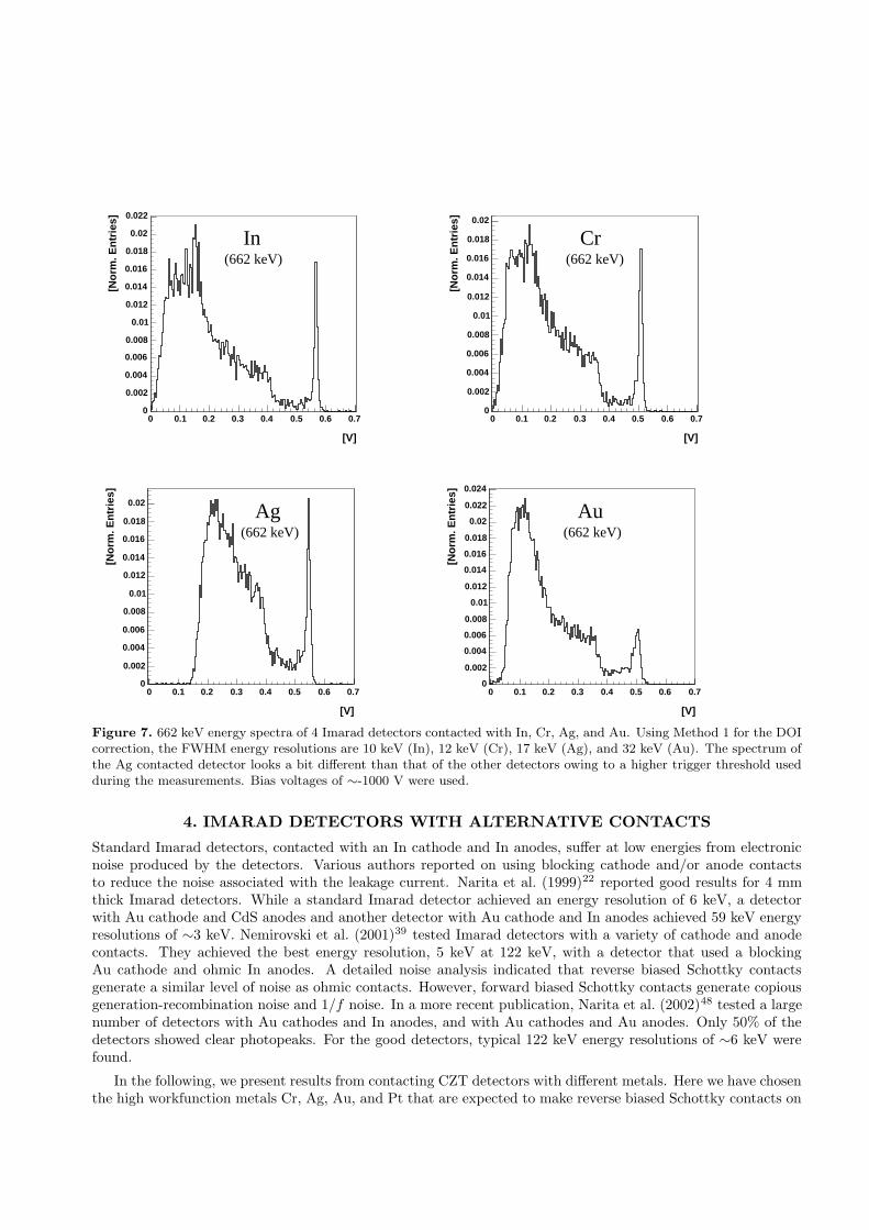
Figure 7. 662 keV energy spectra of 4 Imarad detectors contacted with In, Cr, Ag, and Au. Using Method 1 for the DOIcorrection, the FWHM energy resolutions are 10 keV (In), 12 keV (Cr), 17 keV (Ag), and 32 keV (Au). The spectrum ofthe Ag contacted detector looks a bit different than that of the other detectors owing to a higher trigger threshold usedduring the measurements. Bias voltages of ∼-1000 V were used.
4. IMARAD DETECTORS WITH ALTERNATIVE CONTACTS
Standard Imarad detectors, contacted with an In cathode and In anodes, suffer at low energies from electronicnoise produced by the detectors. Various authors reported on using blocking cathode and/or anode contactsto reduce the noise associated with the leakage current. Narita et al. (1999)22 reported good results for 4 mmthick Imarad detectors. While a standard Imarad detector achieved an energy resolution of 6 keV, a detectorwith Au cathode and CdS anodes and another detector with Au cathode and In anodes achieved 59 keV energyresolutions of ∼3 keV. Nemirovski et al. (2001)39 tested Imarad detectors with a variety of cathode and anodecontacts. They achieved the best energy resolution, 5 keV at 122 keV, with a detector that used a blockingAu cathode and ohmic In anodes. A detailed noise analysis indicated that reverse biased Schottky contactsgenerate a similar level of noise as ohmic contacts. However, forward biased Schottky contacts generate copiousgeneration-recombination noise and 1/f noise. In a more recent publication, Narita et al. (2002)48 tested a largenumber of detectors with Au cathodes and In anodes, and with Au cathodes and Au anodes. Only 50% of thedetectors showed clear photopeaks. For the good detectors, typical 122 keV energy resolutions of ∼6 keV werefound.
In the following, we present results from contacting CZT detectors with different metals. Here we have chosenthe high workfunction metals Cr, Ag, Au, and Pt that are expected to make reverse biased Schottky contacts on

Cathode Anode Contact FWHM(662 keV) FWHM(59 keV)Material Material Deposition
In In Imarad 10 keV 7 keVCr Cr E-Beam 12 keV 11 keVAg Ag E-Beam 17 keV 17 keVAu Au Sputtered 32 keV 5 keVPt In Sputtered 92 keV –
Table 1. FWHM energy resolutions of Imarad detectors contacted with different metals. The Pt–In contacted detectordid not show a clear 59 keV photopeak.
the cathodes of the n-type Imarad CZT. In the case of the Cr, Ag, and Au contacted detectors, we used the samemetal for the anode and the cathode contacts. A fourth detector, called Pt–In detector in the following, wasfabricated from a standard Imarad detector by polishing off the In cathode and replacing it with a Pt cathode,while leaving the In anode contacts untouched.
Using a custom-machined 1.6 mm square punch and 0.3 mm brass foil, we fabricated several masks with 8×8pixels of 1.6 mm pixel diameter and 2.4 mm pixel pitch. The Cr and Ag contacts were applied at WashingtonUniversity. After polishing the detectors with 0.05 µm particle size alumina suspension, the detectors were etchedfor 2 min in 2% Bromide, 20% Lactic Acid, dissolved in Ethylene Glycol.52 After etching, the samples wererinsed in Methanol. Metallization was performed with an electron beam evaporator. The Au and Pt contactswere applied at Fisk University. The Au detector used a blank Imarad detector, with the surfaces polished andprepared by Imarad. The substrate was submerged for 30 sec in 1% Bromide in Methanol, and subsequentlyrinsed in pure Methanol. The Pt–In detector was fabricated from a standard Imarad detector. The cathodewas polished off with 0.05 µm particle size alumina suspension. After polishing, the cathode side was etched 2min in 1% Bromide in Methanol and subsequently rinsed in Methanol. The In contacts were not modified. Thecontacts were deposited with a sputter system.
Energy spectra (662 keV) from relatively good pixels of the standard Imarad detector (In), and the Cr, Ag,and Au contacted detectors are shown in Fig. 7. The four detectors show well pronounced photopeaks, and themean signal amplitudes are very similar for the four detectors. The Pt-In contacted detector showed a ratherpoor performance, and is not included in the figure. At 662 keV, the In contacted detector performs best withan energy resolution of 10 keV. The Cr and Ag contacted detectors exhibit resolutions of 12 keV and 16 keV,respectively. The Au and Pt–In contacted detectors give substantially poorer high energy resolutions of 32 keVand 92 keV, respectively. At 59 keV, we find energy resolutions of 7 keV (In), 11 keV (Cr), 17 keV (Ag), and 5keV (Au). The Pt contacted detector does not exhibit a clear 59 keV photopeak. The results are summarizedin Table 1. For each detector we have tested several pixels. The standard Imarad detector and the Cr andAg contacted detectors exhibit consistent behavior with a ∼10% spread in energy resolutions. The Pt and Aucontacted detectors show a larger spread, with some pixels not giving any photopeaks either at 662 keV or at 59keV, or at both energies.
The Ag, Au, and Pt–In detectors exhibit low leakage currents around 1 nA that are approximately constantfrom 200 V to 1500 V. The Cr detector shows a low leakage current of ∼3 nA when the cathode is positivelybiased with respect to the anode. We measure a large leakage current of 30 nA/1000 V at negative cathode bias.The detector should be refabricated with flipped detector orientation.
5. SUMMARY AND OUTLOOK
CZT has emerged as the detector material of choice for the detection of 10 keV to 600 keV X-rays without theneed for cryogenic cooling. CZT is having a major impact on the field of hard X-ray astronomy. In this paper wehave presented measurements of Imarad CZT standard detectors. We have shown that the cathode amplitudeis better suited to correct the anode amplitudes for the DOI than the duration of the cathode pulse. Aftercorrection for the DOI, the detectors achieve a photopeak efficiency of 67% at 662 keV. The 59 keV and 662 keVenergy resolutions are 7 keV and 10 keV, respectively. We have described first results from contacting Imarad
1 2 3 4 50Energy [kev]
C O Al
Si
Am
plitu
de
1 2 3 4 50Energy [kev]
CdTe
ZnC
OA
mpl
itude
200 Micron
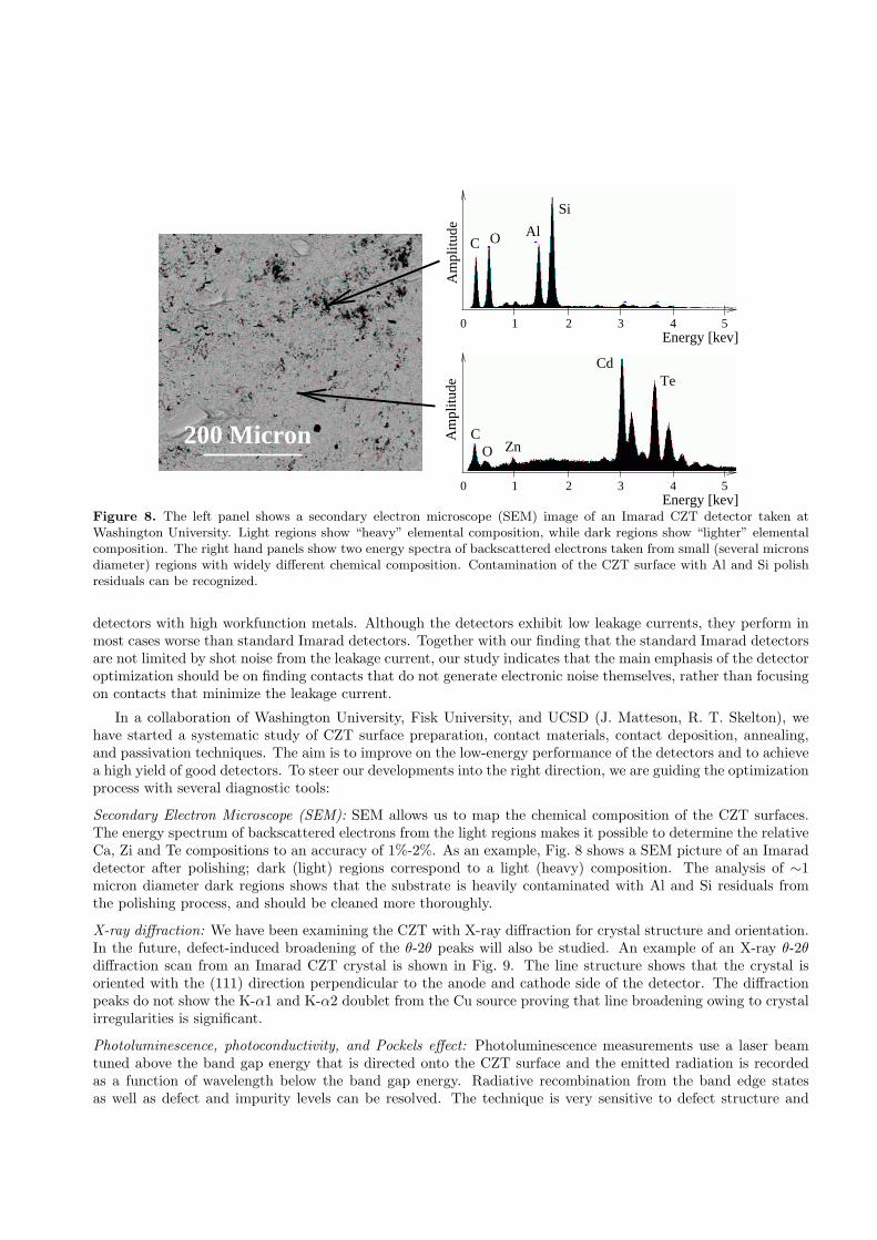
Figure 8. The left panel shows a secondary electron microscope (SEM) image of an Imarad CZT detector taken atWashington University. Light regions show “heavy” elemental composition, while dark regions show “lighter” elementalcomposition. The right hand panels show two energy spectra of backscattered electrons taken from small (several micronsdiameter) regions with widely different chemical composition. Contamination of the CZT surface with Al and Si polishresiduals can be recognized.
detectors with high workfunction metals. Although the detectors exhibit low leakage currents, they perform inmost cases worse than standard Imarad detectors. Together with our finding that the standard Imarad detectorsare not limited by shot noise from the leakage current, our study indicates that the main emphasis of the detectoroptimization should be on finding contacts that do not generate electronic noise themselves, rather than focusingon contacts that minimize the leakage current.
In a collaboration of Washington University, Fisk University, and UCSD (J. Matteson, R. T. Skelton), wehave started a systematic study of CZT surface preparation, contact materials, contact deposition, annealing,and passivation techniques. The aim is to improve on the low-energy performance of the detectors and to achievea high yield of good detectors. To steer our developments into the right direction, we are guiding the optimizationprocess with several diagnostic tools:
Secondary Electron Microscope (SEM): SEM allows us to map the chemical composition of the CZT surfaces.The energy spectrum of backscattered electrons from the light regions makes it possible to determine the relativeCa, Zi and Te compositions to an accuracy of 1%-2%. As an example, Fig. 8 shows a SEM picture of an Imaraddetector after polishing; dark (light) regions correspond to a light (heavy) composition. The analysis of ∼1micron diameter dark regions shows that the substrate is heavily contaminated with Al and Si residuals fromthe polishing process, and should be cleaned more thoroughly.
X-ray diffraction: We have been examining the CZT with X-ray diffraction for crystal structure and orientation.In the future, defect-induced broadening of the θ-2θ peaks will also be studied. An example of an X-ray θ-2θdiffraction scan from an Imarad CZT crystal is shown in Fig. 9. The line structure shows that the crystal isoriented with the (111) direction perpendicular to the anode and cathode side of the detector. The diffractionpeaks do not show the K-α1 and K-α2 doublet from the Cu source proving that line broadening owing to crystalirregularities is significant.
Photoluminescence, photoconductivity, and Pockels effect: Photoluminescence measurements use a laser beamtuned above the band gap energy that is directed onto the CZT surface and the emitted radiation is recordedas a function of wavelength below the band gap energy. Radiative recombination from the band edge statesas well as defect and impurity levels can be resolved. The technique is very sensitive to defect structure and

2 theta [ degree ]
Am
plitu
de
0
100
200
10 20 30 40 50 60 70 80 90 100
Figure 9. The panel shows the X-ray θ-2θ diffrac-tion scan of the “anode” face of an Imarad CZT de-tector taken at Washington University. The diffrac-tion peaks show that the anode and cathode surfacesof the Imarad detectors are oriented parallel to the(111) plane.
impurities from the intrinsic material as well as from any subsequent surface preparation.53 Photoconductivitymeasurements can be used to measure the surface recombination rate.54 These measurements can be combinedwith internal field mapping using the Pockels effect55 and the response to alpha particles. We aim to decouple thecharge loss contributions of the bulk (µ− τ product) and the surface (owing to fabrication related recombinationeffects).
Acknowledgment
We thank Uri El Hanany from Imarad for several free CZT detectors. HK is grateful to J. Matteson for verydetailed discussion of many key characteristics of CZT detectors. It is a pleasure to acknowledge Randy Korotevfor the cross calibration of radio active sources, and Christine Floss for help with the SEM measurements. Thanksto electrical engineer P. Dowkontt, and electrical technician G. Simburger for their work. We acknowledgeL. Sobotka, D. Leopold, and J. Buckley for helpful discussions. This work has been supported by NASA undercontracts NNG04WC176 and NNG04GD70G, and the NSF/HRD grant no. 0420516 (CREST).
REFERENCES
1. Giacconi, R., Gursky, H., Paolini, F. R., et al. 1962, Phys. Rev. Lett., 9, 439
2. Giacconi,R., Branduardi, G., Briel, U., et al. 1979, ApJ., 230, 540
3. Trumper, J. 1983, Adv. Space. Res., 2, No. 4, 241
4. Garmire, G. P., Bautz, M. W., Ford, P. G., Nousek, J. A., Ricker, G. R. Jr. 2003, Proc. SPIE, 4851, 28
5. Struder, L., Briel, U., Dennerl, K., et al. 2001, A&A, 265, L18
6. Matteson, J. L. 1978, Proc. AIAA 16th Aerospace Sciences Meeting, 78
7. Bradt, H. V., Swank, J. H., Rothshild, R. E. 1990, Adv. Space Res., 10, 297
8. Piro, L., Scarsi, L., Butler, R. C. 1995, SPIE Proc., 2517, 169
9. Ubertini, P., Lebrun, F., Di Cocco, G., et al. 2003, A&A, 411, L131
10. Gehrels, N. 2000, Proc. SPIE, 4140, 42
11. NASA’s Structure and Evolution of the Universe 2003 Roadmap, Beyond Einstein: From the Big Bang toBlack Holes, http://universe.gsfc.nasa.gov/
12. The Constellation Project Team, “Constellation-X Technology Readiness and Implementation Plan (TRIP)Report”, http://constellation.gsfc.nasa.gov/images/science/resources/documents/TRIPReport NoCost.pdf
13. Salamon, M. H., private communication
14. Grindlay, J.E., Craig, W.W., Gehrels, N., et al. 2003, Proc. SPIE, 4851, 331
15. McConnell, M., Ryan, J., Macri, J. 2004, Talk at the “Beyond Einstein: From the Big Bang to Black Holes”meeting, Stanford Linear Accelerator Center, Stanford University, 12-15 May 2004

16. eV Products, 373 Saxonburg Boulevard, Saxonburg, PA 16056
17. Imarad Imaging Systems, Ltd., Rabin Park, 10 Plaut Street, Rehovot, Israel
18. Bicron, 6341 San Ignacia Road, San Jose, CA 95119
19. Takahashi, T., Mitani, T., Kobayashi, Y., et al. 2002, IEEE Trans. Nucl. Sci., 49, 1297
20. Bolotnikov, A.E., Chen, C.M.H., Cook, W.R., et al. 2002, IEEE Trans. Nucl. Sci., 49, 1941
21. Macri, J. R., Donmez, B., Hamel, L. A., et al. 2003, IEEE Nucl. Sci. Symposium Conf. Record, 02CH37399,468
22. Narita, T., Bloser, P., Grindlay, J., Jenkins, J., and Yao, H. 1999, Proc. SPIE, 3768, 55
23. Perkins, J. S., Krawczynski, H., Dowkontt, P., Proc. of the 13th International Workshop on Room-Temperature Semiconductor X- and Gamma-Ray Detectors, IEEE Meeting, Portland (OR), 2003, astro-ph/0310910
24. Narita, T., Bloser, P., Grindlay, J., Jenkins, J.A. 2000, Proc. SPIE 4141, 89
25. Varnell, L. S., Mahoney, W. A., Hull, E. L., Butler, J. F. 1996, Proc. SPIE, 2806, 424
26. Wong, A. S., Harrison, F. A., Varnell, L. S. 1996, Proc. SPIE, 2806, 442
27. Hull, E., Pehl, R., Varnell, L. 1997, IEEE Trans. Nucl. Sci., 44, 870
28. Franks, L. A., Brunett, A. B., Olsen, R. W., et al. 1999, NIMA, 428, 95
29. Slavis, K. R., Dowkontt, P., Duttweiler, F., et al. 2000, Proc. SPIE, 4140, 249
30. Parsons, A., Barthelmy, S., Bartlett, L. 1996, Proc. SPIE, 2806, 432
31. Jenkins, J. A., Tomohiko, N., Grinday, J. E. 2003, Proc. SPIE, 4851, 866
32. Murakami, M. M., Kobayashi, Y., Kokubun, M., et al. 2003, IEEE Trans. Nucl. Sci., 50, 1013
33. Fraboni, B., Cavallini, A., Dusi, W. 2003, IEEE 0-7803-8258-7/03
34. Armstrong, W. T., Colborn, L. B., Dietz, L. K., Ramsey, D. B. 1999, Astrophys. Letters and Communica-tions, 39, 413
35. Armstrong, T. W., Colborn, B. L., Ramsey, B. D. 1999, Report SAIC-TN, 990115R3
36. Perfect, C. L., Bird, A. J., Dean, A. J., et al. 2001, Astrophys. & Spa. Sci., 276, 263
37. Bloser, P.F., Narita, T., Jenkins J.A., et al. 2002, Proc. SPIE, 4497, 88
38. Li, W., He, Z., Knoll, G.F., et al. 2001, NIMA, 458, 518
39. Nemirovski, Y., Asa, G., Gorelik, J., Peyser, A. 2001, NIMA, 458, 325
40. Hong, J., Bellm, E. C., Grindlay, J. E.,Narita, T. 2003, Proc. SPIE, 5165, 54
41. Barret, H.H., Eskin, J.D., Barber, ,H.B. 1995, Phys. Rev. Lett., 75, 156
42. Luke, P.N. 1995, ,In: Procs. of the “9th International Workshop on Room Temperature Semiconductor X-and Gamma-Ray Detectors, Associated Electronics and Applications”, Grenoble, France, 18-22 Sept., 1995
43. Nemirovski, Y., Asa, G., Ruzin, A., Gorelik, J., Sudharsanan, R. 1998, Journ. Electr. Materials, 27, 6
44. Luke,P.N., Amman, M., Lee, J.S., Manfredi, P.F. 2001, IEEE Trans. Nucl. Sci., 48, 282
45. Luke, P.N., Lee, J.S., Amman, M., Yu, K.M. 2002, IEEE Trans. Nucl. Sci., 49, 1950
46. Du, Y. F., et al. 1999, IEEE Trans. Nucl. Sci., NS-46, 844
47. He, Z., Li, W., Knoll, G. F., Wehe, D. K., Du, Y. F. 2000, NIMA, 439, 619
48. Narita, T., Grindlay, J. E., Jenkins J. A., et al. 2002, Proc. SPIE, 4497, 79
49. Kalemci, E., Matteson, J. L. 2002, NIMA, 478, 527
50. Agostinelli, S., Allison, J., Amako, K., et al. 2003, NIMA, 506, 250
51. SILVACO International, Inc., 4701 Patrick Henry Drive, Building 2, Santa Clara, CA 95054
52. Wright, G., Cui, Y., Roy, U. N., et al. 2002, IEEE Trans. Nucl. Sci., 49, 2521
53. Leopold, D. J., Ballingall, J. M., Wroge, M. L., 1986, Appl. Phys. Lett., 49, 1473
54. Cui, Y., Groza, M., Hillman, D., Burger, A., James, R. B. 2002, J. Appl. Phys., 92, 2557-2560
55. De Antonis, et al. 1996, IEEE Trans. Nucl. Sci., 43, 1487


![Preliminary Results ofKSU Frisch-Collar CZT ArrayThe KSU CZT array [2] uses 16 individual Frisch-collar detectors for a total volume of -3.4 cm3, but there is no fundamental limit](https://static.fdocuments.us/doc/165x107/5f3e2adcf4b67f1b076eedbd/preliminary-results-ofksu-frisch-collar-czt-array-the-ksu-czt-array-2-uses-16.jpg)