![Hardware implementation of (63, 51) bch encoder and decoder for wban using lfsr and bma [ pdf ]](https://static.fdocuments.us/doc/165x107/5581fd2bd8b42ad3258b48cd/hardware-implementation-of-63-51-bch-encoder-and-decoder-for-wban-using-lfsr-and-bma-pdf-.jpg)
Hardware implementation of (63, 51) bch encoder and decoder for wban using lfsr and bma [ pdf ]
description

LOW POWER TEST PATTERN GENERATION FOR
SYSTEM ON CHIP DEVICES
by
AFTAB FAROOQI, B.S.E.E., M.B.A.
A THESIS
IN
ELECTRICAL ENGINEERING
Submitted to the Graduate Faculty of Texas Tech University in
Partial Fulfillment of the Requirements for
the Degree of
MASTER OF SCIENCE
IN
ELECTRICAL ENGINEERING
Approved
Richard Gale Chairperson of the Committee
Tim Dallas
Accepted
John Borrelli Dean of the Graduate School
May, 2006

ACKNOWLEDGEMENTS
I would like to thank Dr. Gale, my mentor for the entire MSEE
Program, especially for his leadership in guiding me to define the scope of the thesis and helping me identify key milestones towards the completion of the project. Many thanks to Dr. Dallas for helping me break-down the overall thesis project to smaller manageable sub-projects. Thanks to Dr. Nutter for his assistance in helping me experiment the project using Xilinx. Dr. Karp always made herself available to help me decipher signal processing attributes included in the many IEEE papers I had to read for deeper understanding of the issues. Dr. Parten who was always there to help me breakdown complex issues included in the IEEE papers to simple algorithms for better conceptual understanding. Dr. Mitra for her guidance in helping me understand complex mathematical concepts behind signal processing algorithms.
I would like to honor Dr. Chris Monico of the mathematics department for helping me better understand random number generation theory especially the correlation between complex polynomials, matrices and LFSR’s. (Linear Feedback Shift Registers).
ii

Dr. Monico’s assistance was pivotal in helping me grasp the
fundamental mathematical concepts behind a very complex subject of low power pattern generation.
I would also like to thank Dr. Temkin’s candid and sincere steering to help me focus on the fundamental semiconductor manufacturing concepts for stronger technical foundation.
iii

TABLE OF CONTENTS ACKNOWLEDGEMENTS ii ABSTRACT vi LIST OF TABLES viii LIST OF FIGURES ix CHAPTER
I. INTRODUCTION 1
Project Motivation 1 Project Objectives 3 Thesis Outline 4
II. SOC BACKGROUND 6
SOC Attributes 6 SOC Design Tools and Methodology 7 SOC Power Consumption 10 SOC Manufacturing Processes 11 SOC Test and Assembly 13
III. SOC TEST 16
SOC Test Tools and Methodology 16 Test Approaches (External and Conventional
DFT) 18 Built-In-Self-Test (BIST) 19 BIST Pattern Generation Using LFSR 21
IV. LOW POWER PATTERN GENERATION 27
Idea Behind Low Power Test Pattern Generation 27
iv
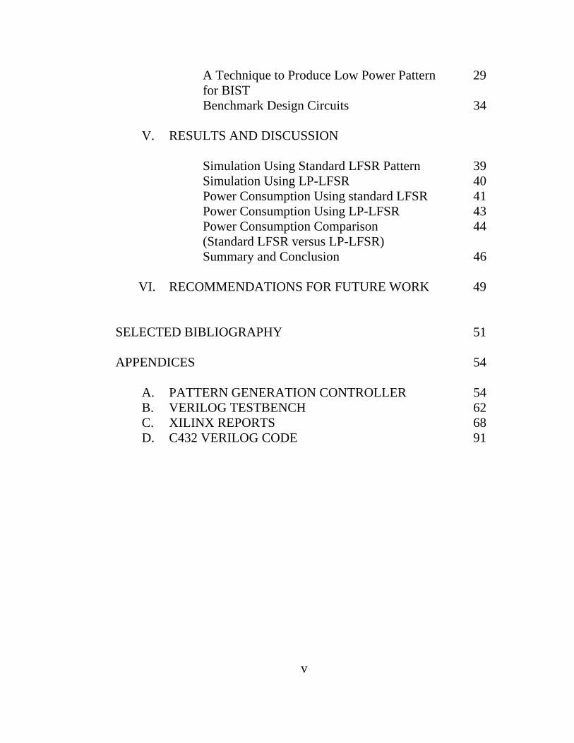
A Technique to Produce Low Power Pattern 29 for BIST
Benchmark Design Circuits 34
V. RESULTS AND DISCUSSION
Simulation Using Standard LFSR Pattern 39 Simulation Using LP-LFSR 40 Power Consumption Using standard LFSR 41 Power Consumption Using LP-LFSR 43
Power Consumption Comparison 44 (Standard LFSR versus LP-LFSR) Summary and Conclusion 46 VI. RECOMMENDATIONS FOR FUTURE WORK 49
SELECTED BIBLIOGRAPHY 51 APPENDICES 54
A. PATTERN GENERATION CONTROLLER 54 B. VERILOG TESTBENCH 62
C. XILINX REPORTS 68 D. C432 VERILOG CODE 91
v

ABSTRACT
State of the art developments in the semiconductor manufacturing processes, integrated chip design methodology, availability of thousand plus pin integrated circuit (IC) packaging options and efficient IC test techniques have contributed immensely towards the integration of entire system on a chip.
These System-On-Chip (SOC) devices can include multiple microprocessors, various types of memories such as SRAM, Flash and ROM, Digital Signal Processor(s), dozens of IP blocks and user defined logic.
Various SOC test techniques have been innovated in the last decade to test complex mixed signal systems on a chip in a cost effective manner. The test industry has made great strides in developing new automated test equipment which can test logic, memory and analog components of the chip via external interface to the IC. Advances in the Built-In-Self-Test (BIST) techniques has enabled IC testing using a combination of external automated test equipment and BIST Controller on the chip.
vi

The power consumption of the chip during manufacturing test can
be significantly higher than the power consumption of the chip in its target system. This increase in the power consumption can be attributed primarily to on-chip extremely random test pattern generation.
This thesis probes into the various IC test approaches such as
external, internal and embedded with specific investigation into the low power test stimulus generation. A new low power pattern generation technique is implemented. Conventional and low power test patterns are applied on an industry standard ISCAS-85 c432 27-channel interrupt controller circuit and average power consumption is measured. The results indicate 60% lower power consumption by the circuit using the new approach for an identical fault coverage of 98% in both cases.
vii

LIST OF TABLES 2.1 ITRS Roadmap by Product 12 3.1 Present/Next State of the Flip-Flops 22 5.1 Power Consumption Analysis 46
viii
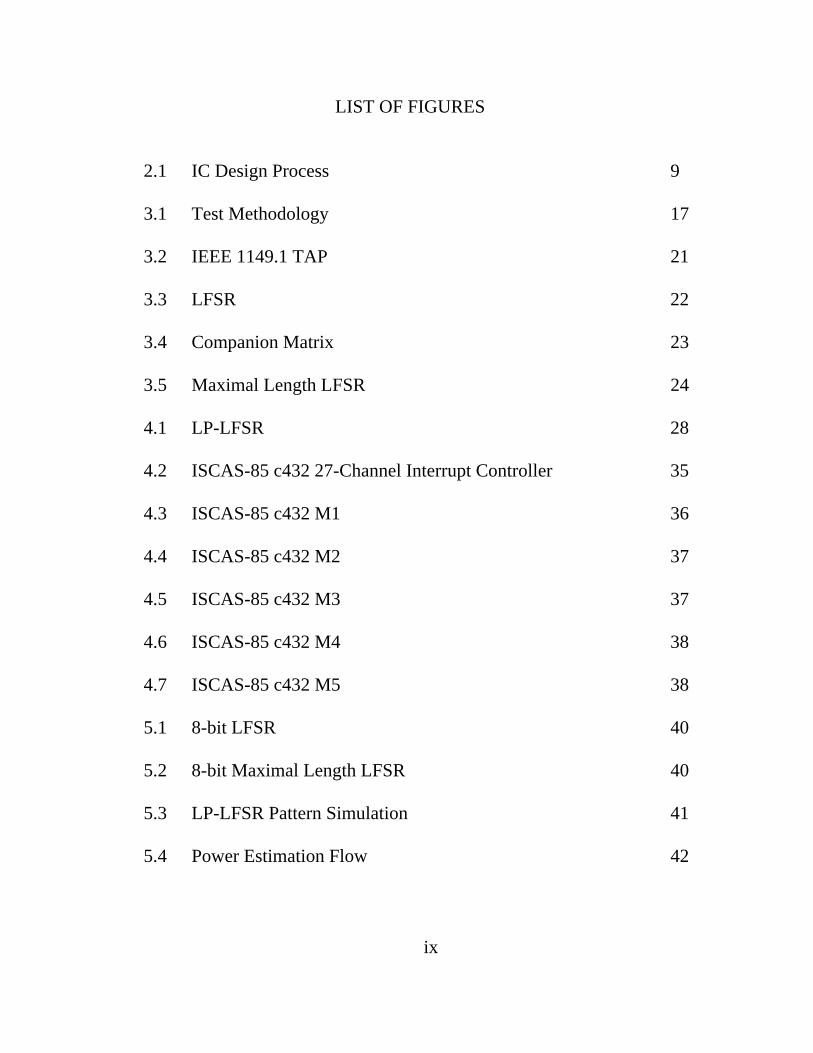
LIST OF FIGURES 2.1 IC Design Process 9 3.1 Test Methodology 17 3.2 IEEE 1149.1 TAP 21 3.3 LFSR 22 3.4 Companion Matrix 23 3.5 Maximal Length LFSR 24 4.1 LP-LFSR 28 4.2 ISCAS-85 c432 27-Channel Interrupt Controller 35 4.3 ISCAS-85 c432 M1 36 4.4 ISCAS-85 c432 M2 37 4.5 ISCAS-85 c432 M3 37 4.6 ISCAS-85 c432 M4 38 4.7 ISCAS-85 c432 M5 38 5.1 8-bit LFSR 40 5.2 8-bit Maximal Length LFSR 40 5.3 LP-LFSR Pattern Simulation 41 5.4 Power Estimation Flow 42
ix

CHAPTER I
INTRODUCTION
Project Motivation
System-On-Chip (SOC) Integrated Circuits (IC’s) are designed and
manufactured to meet application specific functional requirements. Some
examples of applications are camera-on-a-chip, MP3 player, etc. These
functional requirements often need to be balanced with the desired IC
performance, maximum allowable power consumption and overall packaged
and tested IC cost.
Generally total power consumption of the device is a sum of the
power consumed by the core and I/O’s13. Appropriate package
attributes such as the material and thermal properties need to be
selected to ensure maximum heat dissipation of the die through the
package.
IC Architects normally have a specific power consumption budget for
the SOC based on the overall system level power budget. Functional
operation of the device in a system usually consumes power either at or
under the budgeted power for the IC. However the same device under
1

Manufacturing test especially with BIST controller and random pattern
generator can consume more power than the budgeted power1.
This increase in the power consumption of the IC in the test mode is
well known in the industry to cause sudden un-repairable device failures
resulting in significant manufacturing fall-out directly impacting the cost of
the IC.
Today a combination of external Automated Test Equipment (ATE)
and internal BIST (Built-In-Self-Test) techniques are used to ensure the
highest possible fault coverage of the device at the lowest possible cost2,3.
IC testing using exclusively external ATE’s can require SOC
architects to allocate a fairly large number of pins of the device to
invoke the test procedure and run vectors into and through the
various blocks of the device such as memory, user defined
logic, dedicated functional macros, etc. Combination of external
ATE’s and internal BIST however can result in, utilizing far fewer external
pins on the IC but at the cost of embedding test logic inside the device4.
2
Project objectives
Test Pattern generation has long been carried out by using
conventional Linear Feedback Shift Registers (LFSR’s5). LFSR’s are
a series of flip-flop’s connected in series with feedback taps defined by the
generator polynomial6. The seed value is loaded into the outputs of
the flip-flops. The only input required to generate a random sequence is an
external clock where each clock pulse can produce a unique pattern at the
output of the flip-flops.
This random sequence at the output of the flip-flops can be used as a
test pattern. The number of inputs required by the circuit under test must
match with the number of flip-flop outputs of the LFSR. This test pattern is
run on the circuit under test for desired fault coverage.
The power consumed by the chip under test is a measure of the
switching activity of the logic inside the chip which depends largely on the
randomness of the applied input stimulus. Reduced correlation between the
successive vectors of the applied stimulus into the circuit under test can
result in much higher power consumption by the device than the budgeted
power. A new low power pattern generation technique is implemented using
a modified conventional Linear Feedback Shift Register7.
3

Conventional as well as low power test patterns are run on an industry
standard benchmark circuit. The instantaneous and peak power
consumption8 of the circuit is measured using industry standard Xilinx
tool called xPower and it is demonstrated that the new low power approach
results in significantly lower power consumption by the circuit under
test compared with the power consumption by the circuit using the
conventional pattern for the same fault coverage.
Thesis outline
Chapter 2 reviews SOC’s and their attributes with some insight into
the application specific Intellectual Property (IP) requirements. It also
provides an overview of the IC manufacturing processes, design/test tools
and methodology, discusses the various types of power consumed by the
device during normal operation and under manufacturing test. It also
provides a brief insight into the chip assembly process.
Chapter 3 investigates into the IC test tools and methodology
particularly external, internal and a combination of external/internal
approaches. The concept of BIST architecture and its components is
explained along with the explanation of LFSR, a circuit very commonly
4
used to generate random test patterns. The correlation of the LFSR, its
characteristic polynomial and matrix theory is described9,10.
Chapter 4 begins with a description of a pattern generated using a
conventional LFSR. It explains in detail the idea behind the low power
pattern generation in particular the low power technique designed using two
levels of logic between the outputs of the LFSR and the actual outputs
coming out of the second level of logic. Standard tools such as Verilog
HDL, Xilinx, and Mentor’s Modelsim are used for design description,
synthesis, simulation and power consumption estimation. A brief
background of the commonly used industry standard benchmark circuits is
also provided.
Chapter 5 begins with the methodology used to determine the power
consumption by the c432 benchmark circuit using the conventional pattern.
It explains the methodology used for computing power consumption by the
ISCAS-85 benchmark circuit c432 (27-channel interrupt controller) using
the low power pattern. A comparison of the circuit power consumption is
discussed between the two techniques.
Chapter 6 provides some recommendations on future work.
5
CHAPTER II
SOC BACKGROUND
SOC Attributes
SOC’s typically integrate multiple Microprocessors, various types of
memories such as SRAM, ROM, Flash, user defined logic, etc. Most SOC’s
are heavily populated with multiple instances of memory. Also included can
be IP macros such as Digital Signal Processors, Analog to digital
converters, etc11.
SOC’s typically contain multiple types of I/O’s ranging from standard
CMOS, LVTTL to high speed I/O’s such as LVDS (Low voltage differential
signal).
The pin count can range from a few hundred pins to over a thousand
with custom designed packages including multiple layers of substrate.
SOC’s are solution driven with the intent of providing a single chip solution
for particular applications such as digital cameras, MP3 players, storage
drives, printers, networking, etc. SOC’s for the Consumer electronics
typically include mixed signal components such as A/D, D/A,
multiple instances of SRAM, Flash, ROM and user defined logic.
6

Networking and Storage applications tend to be extremely compute
intensive and therefore it is not uncommon to find these devices containing
multiple microprocessor cores along with many megabits of memory and
high speed I/O’s operating in the giga-bit per second range.
Increasing the complexity of the SOC designs besides higher level of
IP integration are other factors such as multiple clock domains ranging from
a few kHz to as high as few GHz. Each clock domain is typically responsible
for running a specific portion of the chip12.
Power consumption of the device normally includes power consumed
by the core of the chip plus power consumed by the I/O’s13. Most SOC die
are packaged in multiple substrate packages with some level of signal
routing in the package substrates. Various types of packages such as Quad-
Flat-Packs, Ball Grid Arrays, etc can be custom designed (e.g. Plastic or
Ceramic) to meet the required power dissipation of the SOC die.
SOC Design Tools and Methodology
Generally the architecture of the entire SOC is designed and simulated
by chip architects. Front end designers are involved in converting the
7

architecture level IC requirements to detailed circuit level descriptions using
design description languages such as Verilog, VHDL, etc. Depending
on the complexity of the overall IC project, it is not uncommon to find front
end design teams ranging from ten’s of engineers to a few hundred spending
anywhere from 6 months to a year on the entire device design.
Back-end Design Engineering typically entails converting the circuit
level description to a physical description format used by the foundries for
IC Manufacturing. Again this task can also require a large number of
engineers depending on the physical size of the chip.
The entire SOC is simulated at an architecture level for the required
functional performance. Individual modules are synthesized and verified for
their respective functionality. Design verification is performed iteratively
before and after each stage of the entire IC design (Front-End to Back-End)
process. Verification results are compared between the pre and post
processing of each design stage to ensure compliance to the required
specification and easier root cause analysis in case of any errors.
Figure 2.1 below shows typical IC Design methodology before the
formal hand-off to the foundry for manufacturing. The methodology
includes Design Description, Logic Synthesis and Optimization, Pre-Layout
8

Simulation, Place and Route, Post Layout Simulation, DRC/LVS, GDS11
and mask generation.
Figure 2.1 IC Design Methodology
9

It is important to note that continuing advances in the inclusion of the
advanced Manufacturing process parameters in the front end IC Design
libraries and tools is expected to shrink the gap between the Front-end and
Back-end design tasks. This can result in requiring Front-end Design
Engineers to perform their tasks conforming to not only circuit design
limitations but also compliant to manufacturing constraints.
In addition to design for manufacturing, design for test approach is
mandating the chip design and test architects to include built-in self-test
controllers and test pattern generation inside the chip. While this mandate
can result in many benefits such as lower cost of test, etc it can also increase
the die size and power consumption.
SOC Power Consumption
Estimating the IC power budget involves maintaining perspective of
several technical and business factors such as process technology, cell
design libraries, pin-out and package constraints, logic and IP macro clock
domains, cost and time pressures, etc.
10

IC architects are required to select the optimum combination of these
elements to be able to achieve not only a functional device but also cost
competitive and meeting customer schedule.
Total power consumption of the CMOS device is the sum of static
power, dynamic power, leakage and short crcuit11. Static power can be
defined as the power consumed by the CMOS gate under no switching
activity. It is normally attributed to the leakage currents in the device.
Dynamic power on the other hand is a direct result of the switching
activity of the gate and is generally most of the power consumed by the
device. The more the gates toggle or change states under various load
conditions, the more dynamic power is consumed. Short circuit power of the
cell is caused by the temporary short circuit between the N and P transistors
of the gate during logic transitions.
SOC Manufacturing Processes
As evident in Table 2.1 below CMOS Manufacturing process
technology developers have made remarkable strides in shrinking the gate
length with majority of the present day SOC’s manufactured in 0.18 and
11

smaller process geometries. It is common to find devices using both Al and
Cu interconnects with low-k dielectric materials.
Table 2.1 ITRS roadmap by Product
Year of Production 2005 2006 2007 2008 2009 2010 2011 2012 2013DRAM stagger-contacted Metal 1 M1 1/2 pitch (nm) 80 70 65 57 50 45 40 36 32MPU/ASIC stagger-contacted Metal M1 1/2 pitch (nm) 90 78 68 59 52 45 40 36 32Flash Uncontacted Poly Si 1/2 pitch (nm) 76 64 57 51 45 40 36 32 28MPU Printed Gate Length (nm) 54 48 42 38 34 30 27 24 21MPU Physical gate Length (nm) 32 28 25 23 20 18 16 14 13
Sub nanometer manufacturing technologies have enabled millions of
transistors to be packed in few millimeter squared die sizes. The ability to
manufacture these many transistors has driven the integration of entire sub-
systems and in most cases complete systems on a chip.
On the other hand EDA tool developers have kept up with their pace
on developing advanced tools linking Design for Test and Design for
Manufacturing. More than a decade old concept of Design for Test has been
extended to Design for Manufacturing.
Today there are tools available to validate the Manufacturing viability
of the designs before getting to the Foundry18.
12

The advanced ability to estimate the yield of the chip with circuit
design as well as manufacturing constraints has resulted in significant cost
savings in the entire supply chain of IC design and manufacturing.
The cell library and IP developers have diligently kept up with the
design and development of the various types of libraries such as low power,
small size, etc and cores such as Microprocessors, DSP’s, Memories, etc
respectively. The ability to select and integrate pre-verified silicon proven
IP blocks on a single substrate has made significant contribution toward the
design and production of entire systems on a chip for a variety of market
applications.
SOC Test and Assembly
The scope of IC test can range from wafer level (ensure good wafer)
testing to individual die on the wafer and at the packaged chip level. The
selection of a type and/or a combination of these tests can be driven by
multiple factors such as the complexity of the chip, test cost, price of the
chip as determined by the market, etc. For example it may be cost
prohibitive to run very small chip (order of few thousand gates in a small 48-
pin QFP package targeted for market price of sub $1) through each of these
13

phases. The total test cost for these phases combined can easily surpass the
individual die or package cost resulting in the price of the chip deemed un-
bearable by the market3.
Design for Test is a common approach used in architecting and
implementing complex SOC’s. IP level (Microprocessors, A/D, PLL,
Memory, etc) functional verification and manufacturing tests are often
performed by the IP providers before the IP is integrated into the SOC.
SOC Designers however still need to include test logic on the chip to be
able to test the IP in the overall system design environment.
User-defined Logic is commonly verified using an FPGA before
integrating it on the chip. Again it is incumbent upon the SOC design team
to include logic for test on the chip to test user defined logic along with the
other blocks of the chip.
A combination of external testing using Automated Test Equipment
and internal testing using memBIST , LogicBIST, IPBIST, SCAN, etc
techniques are used to verify the overall functionality of the SOC.
Die and Package assembly is a function of the die size and type of
package. Commonly used package types include QFP’s and BGA’s. The
cavity of the package is indicative of the die size that can be accommodated
14

in the package. SOC suppliers can choose to test the IC at the package level
and ignore tests at the wafer and/or die level. This is primarily done to save
costs. (SOC cost is the sum of the die, package and test/assembly cost).
15

CHAPTER III
SOC TEST
SOC Test Tools and Methodology
As noted in chapter 2 it is imperative to verify the functional and
manufacturing viability of the individual IP components before integrating
them into the SOC design. Most cores are offered with the wrapper logic
around the IP which is used as the interconnect between the design blocks.
Internal design details of IP macros are typically not shared by the IP
provider as that information is considered confidential.
SOC testing is best viewed as an iterative process comprised of a
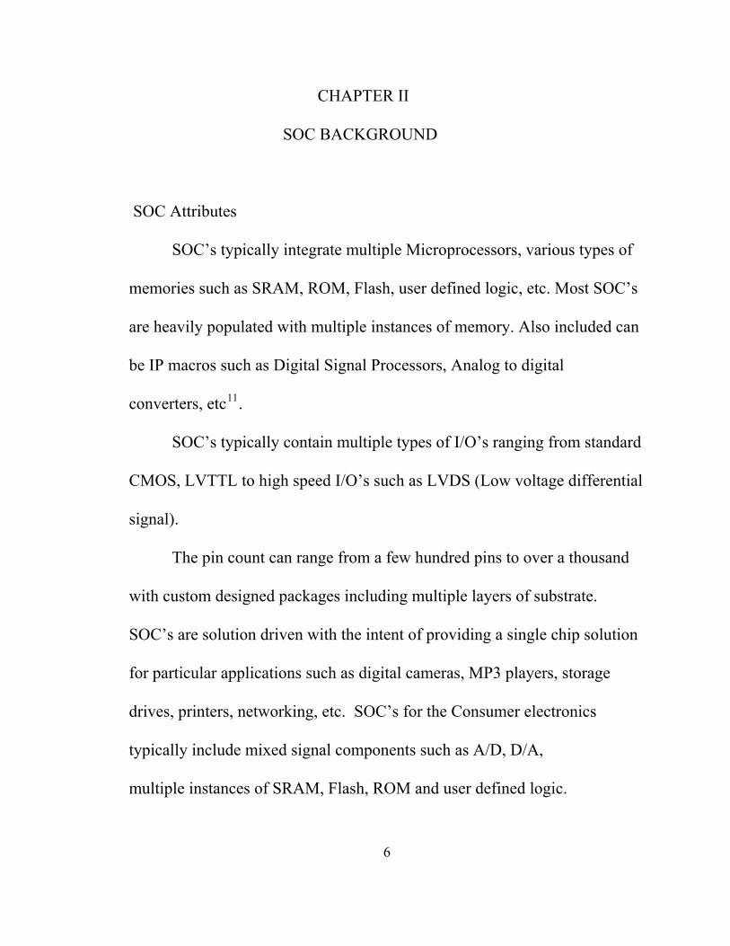
series of tests. Figure 3.1 shows a test methodology. Either flat or
hierarchical approach can be used depending on the complexity of the device.
As the complexity of the device increases it is often recommended to test
individual components using Scan and/or BIST as opposed to testing the
entire design using a flat approach. The flat approach would essentially
flatten the entire design’s netlist, apply stimulus at the primary inputs of the
design and test outputs at the primary outputs. This approach does not
16
provide the ability to observe the logic at the interconnects between the
various blocks of the design.
Figure 3.1 Test Methodology
An advantage of testing the SOC using a hierarchical approach is its
inherent ability to isolate and correct the problem piecewise. Test input
stimulus is applied to a particular macro with the outputs observed and
verified.
17

External ATE testers can include Logic, Memory, Processor and
Mixed-signal test specific boards. Conventional Design for test approaches
include Scan and Built-In-Self test. Most SOC designs today however
include an embedded test approach which involves using a combination of
external low cost Digital tester and on-chip test logic for stimulus generation,
output analysis and compression, diagnostics, timing, power management,
etc14.
Test Approaches (External ATE, Conventional DFT and Embedded4 )
Embedded test is a natural evolution of the two distinct approaches
discussed thus far namely external ATE and DFT. External ATE approach
requires a mix of very expensive low/high speed testers with varying
bandwidth. These testers can be configured to provide function specific test
ability for high speed logic, memory, analog to digital converters, etc.
DFT approach on the other hand is predominantly based on using
Scan and BIST test architectures. Scan test involves replacing the generic
flip-flops of the design with scan enabled flip-flops along with the insertion
of multiple scan chains around the design. Test input stimulus can be
18

propagated either through the individual portion of the design or the entire
device for functional verification.
Embedded test integrates the high speed and high bandwidth portions
of the external ATE directly into the IC and can be considered as the main
objective of the embedded test approach. Automatic test pattern
generation/Fault Simulation tools can be used to generate, integrate, analyze
and verify test pattern development.
One of the key benefits of the embedded test is in the on-chip test data
generation which reduces the volume of external patterns and can be
customized per the IP block type in the SOC. On-chip go/no-go and data
compression reduces ATE data logging. On-chip timing generation achieves
true at speed tests that can be scaled to match manufacturing process
technology performance. The downside of on-chip data generation however
is the increase in the power consumption of the device in the test mode.
Built-In Self Test (BIST)
BIST is a hierarchical DFT strategy that reduces the need for external
test. With BIST a micro-tester complete with a pattern generator is brought
onto the chip enabling the chip to test itself. Although the micro-tester
19

requires more silicon area, the savings realized through automation of the
testing process makes this DFT method very attractive.
BIST logic is composed of pattern generation, pattern capture and
compare and self test control. BIST can be used for low speed as well as
high speed testing. BIST uses on-chip controllers for memory, logic, etc.
These controllers are typically accessed via an external interface defined by
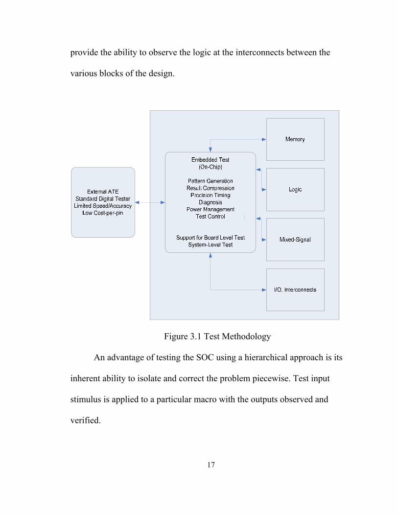
the various IEEE standards. IEEE standard 1149.1 as shown in Figure 3.2
defines the test access port composed of 5 external pins for initializing BIST
operation, monitoring and reading results.
The benefits of BIST are higher quality testing, faster time to market
and lower costs. Chips can be tested at speed without incurring yield losses
because of tester inaccuracy. BIST automates a higher degree of the test
development process and simplifies the development of test programs. BIST
reduces the dependency on expensive ATE. High end ATE costs are
approximately five million U.S. dollars. This need is attributed to more
memory to store large patterns, faster pin electronics, BIST solves the ATE
cost problem by moving data directly onto the chip4.
20
Figure 3.2 IEEE 1149.1 TAP
BIST Pattern Generation using LFSR
Linear Feedback Shift Register is a circuit consisting of flip-flops
connected in series with each other. The output of one flip-flop is connected
to the input of the next flip flop and so on. The feedback polynomial which
is also known as the characteristic polynomial is used to determine the
feedback taps which in turn determines the length of the random pattern
generation.
An example below in Figure 3.3 is used to illustrate a correlation
between the LFSR, its characteristic polynomial and matrix theory. In the
circuit the feedback taps are shown to be from the output of the 4th and 1st
register.
21

Figure 3.3 LFSR
These taps are indicative of the generator polynomial. According to
this polynomial the present and the next state of these registers are shown in
Figure 3T(R1, R2, R3, R4 and R1=R1⊕R4, R2 = R1, R3 = R2 and R4 =
R3).
Table 3.1 Present/Next State
Present State
Next State
R1 R1 ⊕ R4 R2 R1 R3 R2 R4 R3
Using the matrix theory the companion matrix required for relating
the present to the next state is depicted in Figure 3.4 below. The actual
sequence of the LFSR is represented as BT, BT2, BT3, ….where B is the
22

seed vector. The determinant of the T matrix is called the characteristic
polynomial and the generator polynomial is the inverse of the characteristic
polynomial.
1 0 0 1
1 0 0 0
0 1 0 0
0 0 1 0
Figure 3.4 T Companion Matrix
Det(T) = [xI – T] {Characteristic Polynomial}
Where I is the identity matrix
Generator Polynomial = Inverse of the Characteristic Polynomial
As an example the characteristic polynomial for the above circuit is =
X4 + X3 + 1 and the generator polynomial is represented as X4 +X +1.
Normally the feedback taps are selected such that entire sequence is
generated including all zeros and one’s. The generation of all zero’s pattern
requires an additional NOR gate whose inputs are the outputs of all flip-
23

flops in the LFSR. The output of the NOR gate is fed into the input of the
first flip-flop in the circuit as shown in Figure 3.5.
Figure 3.5 Maximal Length LFSR
The outputs of the LFSR are initially loaded with a combination of 1’s
and 0’s normally referred to as the seed vector. Proper selection of the
generator polynomial is important in order to ensure the generation of the
entire sequence. Common Clock signal is applied to the entire chain of flip-
flops which essentially enables the propagation of the logic values present at
the inputs to the flip-flop outputs. These random outputs are used as the
input stimulus for circuit to be tested.
Normally this random pattern can be propagated through a known
24

good circuit and the output of the circuit is captured using a MISR (Multi-
Input Shift Register). The MISR output also known as the good signature is
then used to compare with the signature obtained for other similar circuits.
One of the drawbacks of generating a pattern using the above
approach is the reduced correlation15 between the bits (output bits of the
LFSR) of the successive vectors. This can attribute to one of the key
differences between the vectors used for functional verification of the IC in
the system environment compared to the vectors used in the manufacturing
test environment.
In a functional operation environment, the input stimulus is generated
by the component(s) of the system interfacing with the device under test and
therefore can have better correlation between the successive vectors.
Additionally the number of vectors generated in a functional test
environment can be much lower than the number of vectors generated by the
LFSR. This increase in the number of test vectors combined with reduced
correlation between the bits can result in significant increase in the switching
activity of the circuit under test and therefore increased power consumption
of the device in the Manufacturing Test environment.
25

The increased power consumption by the device in the manufacturing
test environment therefore can in most cases exceed the maximum power
consumption specification of the IC resulting in un-repairable device failures
begins with a pattern generated using a conventional LFSR causing
significant loss of yield.
26

CHAPTER IV
LOW POWER PATTERN GENERATION
Idea behind low power test pattern generation
One way to improve the correlation between the bits of the successive
vectors is to avoid frequent transitioning of the logic levels (1 0 or 0 1)
of the primary inputs.
The new approach entails inserting 3 intermediate vectors between
every two successive vectors. The total number of signal transitions between
these 5 vectors is equal to the total number of signal transitions between the
2 successive vectors generated using the conventional approach. This
reduction of signal transition activity in the primary inputs reduces the
switching activity inside the design under test and therefore results in
reduced power Consumption by the device under test.
The additional circuitry used to accomplish the generation of the 3
intermediate vectors is minimal at best consisting of few logic gates.
The pattern generation controller which is designed using Verilog as
shown in Appendix A can be very easily modified for the required number
of LFSR outputs.
27
The number of LFSR outputs required is driven by the number of test
inputs required for circuit under test.
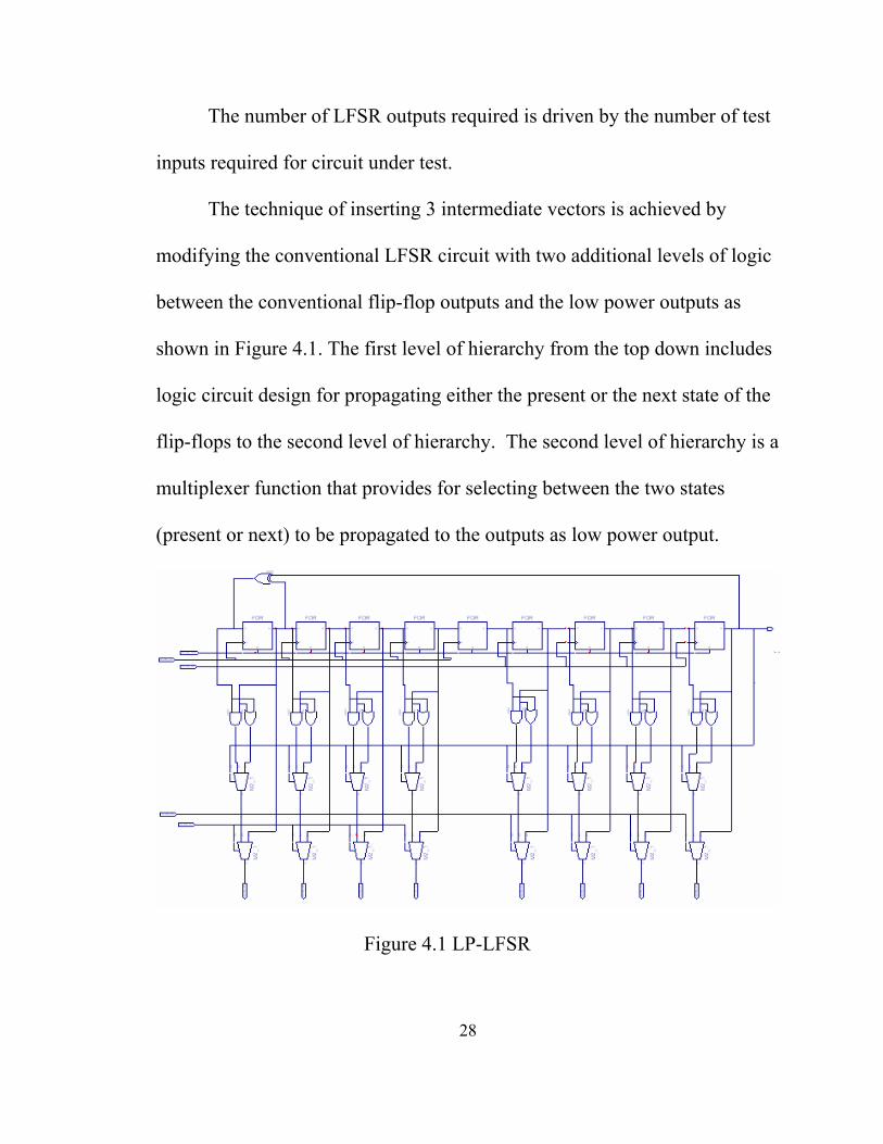
The technique of inserting 3 intermediate vectors is achieved by
modifying the conventional LFSR circuit with two additional levels of logic
between the conventional flip-flop outputs and the low power outputs as
shown in Figure 4.1. The first level of hierarchy from the top down includes
logic circuit design for propagating either the present or the next state of the
flip-flops to the second level of hierarchy. The second level of hierarchy is a
multiplexer function that provides for selecting between the two states
(present or next) to be propagated to the outputs as low power output.
Figure 4.1 LP-LFSR
28
In the simulation environment, the outputs of the flip-flops are loaded
with the seed vector. The feedback taps are selected pertinent to the
characteristic polynomial x8 + x + 1. Only 2 inputs pins, namely test enable
and clock are required to activate the generation of the pattern as well as
simulation of the design circuit. It is also noteworthy here that the
intermediate vectors in addition to aiding in reducing the number of
transitions can also empirically assist in detecting faults just as good as the
conventional LFSR patterns.
Description of the technique to produce low power pattern for BIST
The following is a description of a low power test pattern generation
technique as depicted in the 9-bit LFSR based schematic in Figure 4.1.
Verilog based test bench as shown in Appendix B is used in assigning the
initial output states (0100 1011) of the 9-bit LFSR. The feedback taps are
designed for maximal length LFSR generating all zeros and all one’s as well.
The first step is to generate T1, the first vector by enabling (clocking)
the first 4-bits of the LFSR and disabling (not clocking) the last 4 bits. This
Shifts the first 4 bits to the right by one bit. The feedback bits of the LFSR
are the outputs of the 8th and the first flip-flop. The output of the 8th flip-flop
29

is 1 and the output of the first flip-flop is 0. The exclusive-or of the
8th-flip-flop (logic 1 in this case) and the first flip-flop(logic 0 in this case) is
input (1 EXOR 0 = 1 into the first D flip-flop. The new pattern in the first
four bits of the LFSR is 1010. Note that the shaded register is clocked along
with the first 4 bits of the LFSR. So the input of the shaded flip-flop is the
output of the 4th flip-flop which in this case is 0.
Also note that prior to the first clock, the input of the shaded register
was the seed value of the 4th flip-flop at the output of the 4th flip-flop which
in this case is 0. So after the first clock this value of 0 will now appear at the
output of the shaded flip-flop. In other words the value of the 4th output is
stored in this shaded register and is used in the next few steps.
The first 4 shifted bits of the LFSR and the last 4 un-shifted bits (i.e.
the seed value) are propagated as T1 (1010 1011) to the final outputs.
Next few steps involve generating the 3 intermediate patterns from T1.
These patterns are defined as Ta, Tb and Tc.
Ta is generated by maintaining (disabling the clock to the first 4 bits)
the first four bits of the LFSR outputs (as is from T1) as the final first four
low power outputs 1010. Note that the clock to the last four bits of the LFSR
is also disabled. The last four bits however are the outputs from
30
the injector circuits. The injector circuit compares the next value
(@ the input of the D-flip-flop) with the current value (@ the output of the
D-flip-flop).
According to T1, the outputs (current values) of the last 4 bits of the
LFSR are 1011. The next values are the values at the inputs of the D-flip-
flops which in this case are 0101. Compare the current values (1011) bit by
bit with the next values (0101). If the values bit by bit are not the same then
use the random generator feedback R (in this case is logic 1) as the bit value
as shown in the schematic above. If however both values bit by bit are the
same then propagate that bit value to output as opposed to the R bit. This
bit by bit comparison gives us the last four bits of Ta to be 1111. Therefore
Ta = 1010 1111.
Next step is to generate Tb. Shift the last 4 flip-flops to the right one
bit but do not shift the first 4 flip-flops to the right. The clock to the first 4
bits plus the shaded flip-flop is disabled. The clock to the last 4 bits is
enabled.
Propagate the outputs of the flip-flops of the entire LFSR as opposed
to the outputs of the injection circuit to the outputs (low power). The
injection circuits are disabled.
31

As in Ta, maintain the first four LFSR outputs (1010) as the low
power outputs. Again from Ta, the inputs of the last four D flip-flops
from the previous step (generating Ta) are 0101. Also note that the output of
the shaded register is 0 from the previous step (generating Ta). Therefore the
input of the 5th flip-flop is a 0. The outputs of the last 4 flip-flops are
0101 resulting in Tb = 1010 0101.
The 3rd intermediate vector Tc is generated via disabling the clock to
the entire LFSR. Propagate the first 4 outputs from the injection circuit as
the first 4 low power outputs and maintain the last 4 low power outputs the
same as Tb. Generating injection circuit outputs for Tc is conceptually the
same as explained above in generating Ta. Current values (@ the outputs of
the flip-flops) of the first four flip-flops are compared with the next values
(@ the inputs of the flip-flops) of the flip-flops.
The feedback from the 8th flip-flop is 1 (please see generating Tb).
Therefore the logical feed forward value of R is 1. The feedback value from
the first flip-flop is also 1 as per the current values above. The exclusive
or of two ones is a 0. Therefore the input to the first flip-flop is a 0 which is
also the next state of the first flip-flop. Hence the next values are 0 for the
first flip-flop and 101 for the 2nd, 3rd and 4th flip-flop respectively. The next
32
values are 0101.
The first four outputs from the injection circuit are 1111. The last 4
outputs are the same as Tb which are 0101 resulting in the 3rd and final
intermediate vector Tc = 1111 0101.
Generating T2 is quite similar to generating T1. As in Tc the outputs
of the last four LFSR flops are 0101. The outputs of the first 4 flip-flops of
the LFSR are the current values which are 1010. Therefore the seed vector
for generating T2 is 1010 0101.
Shift the first four bits of the LFSR plus the shaded flip-flop. Do not
clock the last four flip-flops. Propagate the outputs of the entire LFSR to the
final low power outputs.
The output of the 8th flip-flop from the previous step (generating Tc)
is a 1 and the output of the first flip-flop from the previous step (generating
Tc) is also a 1. The exclusive or of the output of the 8th flip-flop and the first
flip-flop is 0.
Therefore the input to the first flip-flop will be a 0. The inputs to the
2nd, 3rd , 4th and the shaded flip-flops are 1010. These are also the current
values from the previous step (generating Tc). Shifting the first four flip-
flops of the LFSR to the right by one bit results in 0101 as the outputs of the
33

first four flip-flops. Therefore T2 generated is 0101 0101. This concept of
low power pattern generation is extended to 36-bits required for the design
circuit indicated in section 4.3.
Benchmark Design Circuits
Several Industry standard benchmark circuits such as ISCAS-85,
ISCAS-89, etc can be used to test new design, test and manufacturing
approaches and technologies. Following is a brief description of one of the
ISCAS-85 circuits used for the purpose of testing the new low power pattern
generation scheme described above.
c432 is a 27-channel interrupt controller. The input channels are
grouped into three 9-bit buses (we call them A, B and C), where the bit
position within each bus determines the interrupt request priority. A forth 9-
bit input bus (called E) enables and disables interrupt requests within the
respective bit positions. Figure 4.4 below shows the c432 circuit. Figures 4.5
to 4.9 below show the logic of the underlying modules.
34
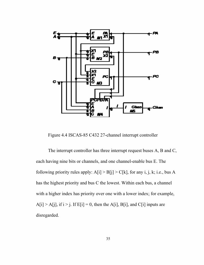
Figure 4.4 ISCAS-85 C432 27-channel interrupt controller
The interrupt controller has three interrupt request buses A, B and C,
each having nine bits or channels, and one channel-enable bus E. The
following priority rules apply: A[i] > B[j] > C[k], for any i, j, k; i.e., bus A
has the highest priority and bus C the lowest. Within each bus, a channel
with a higher index has priority over one with a lower index; for example,
A[i] > A[j], if i > j. If E[i] = 0, then the A[i], B[i], and C[i] inputs are
disregarded.
35
The seven outputs PA, PB, PC and Chan[3:0] specify which channels
have acknowledged interrupt requests. Only the channel of highest priority
in the requesting bus of highest priority is acknowledged. One exception is
that if two or more interrupts produce requests on the channel that is
acknowledged, each bus is acknowledged. For example, if A[4], A[2], B[6]
and C[4] have requests pending, A[4] and C[4] are acknowledged. Figure
4.9 is a 9-line-to-4-line priority encoder.
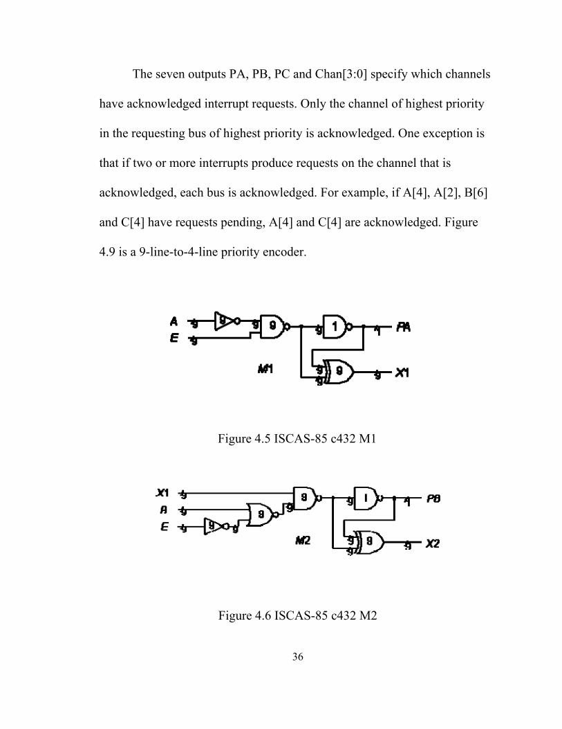
Figure 4.5 ISCAS-85 c432 M1
Figure 4.6 ISCAS-85 c432 M2
36

Figure 4.7 ISCAS-85 c432 M3
Figure 4.8 ISCAS-85 c432 M4
37
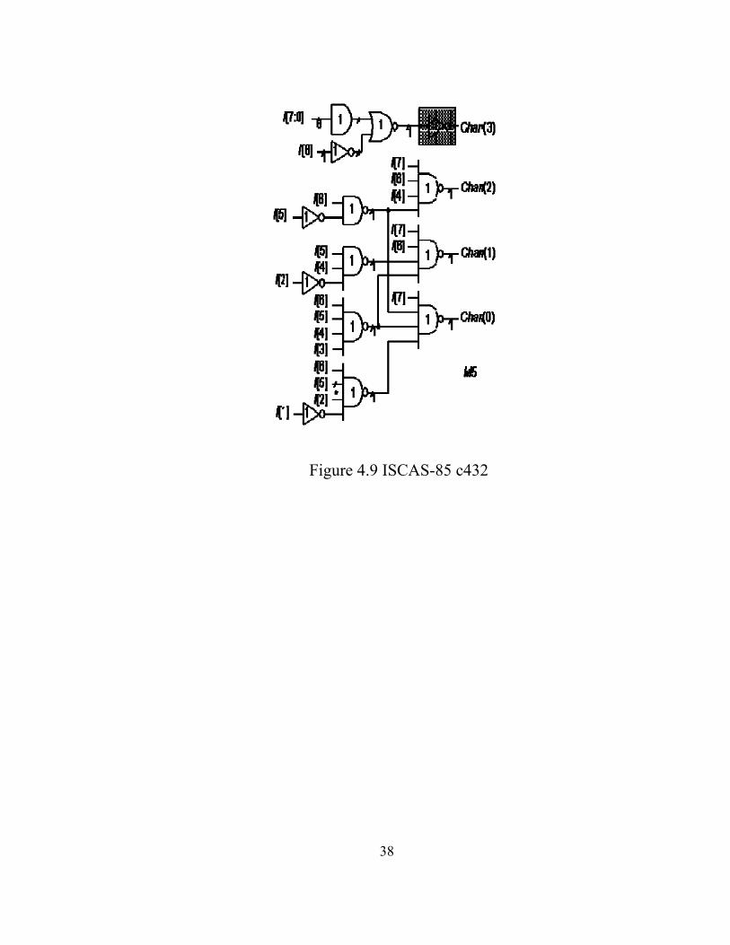
Figure 4.9 ISCAS-85 c432
38

CHAPTER V
RESULTS AND DISCUSSION
Simulation using standard LFSR pattern
The standard 36-bit pattern is generated using the LFSR configuration
as shown in figure 5.1 below. The schematic in the case of conventional
pattern generation consists of 36 flip-flops connected in series. The design is
modified as indicated in figure 5.2 below with feedback taps to generate a
maximal length pattern generator including all 0’s and 1’s. The number of
vectors expected in this case are 236. The outputs of the 36-bit LFSR are
used as the inputs to the c432 ISCAS-85 interrupt controller design circuit.
A common clock is supplied to all flip-flops. A seed value is assigned to the
output of each flip-flop. Each clock pulse thereafter shifts the logic value
present at the input of the flip-flop to its output.
39
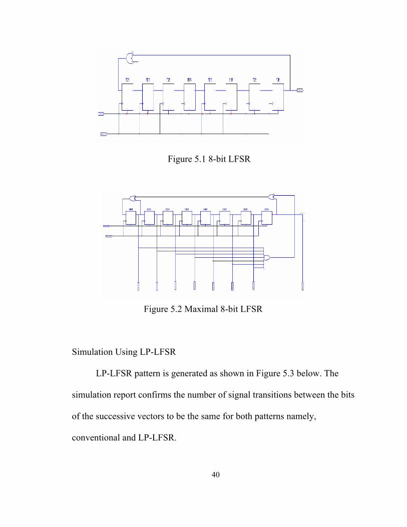
Figure 5.1 8-bit LFSR
Figure 5.2 Maximal 8-bit LFSR
Simulation Using LP-LFSR
LP-LFSR pattern is generated as shown in Figure 5.3 below. The
simulation report confirms the number of signal transitions between the bits
of the successive vectors to be the same for both patterns namely,
conventional and LP-LFSR.
40
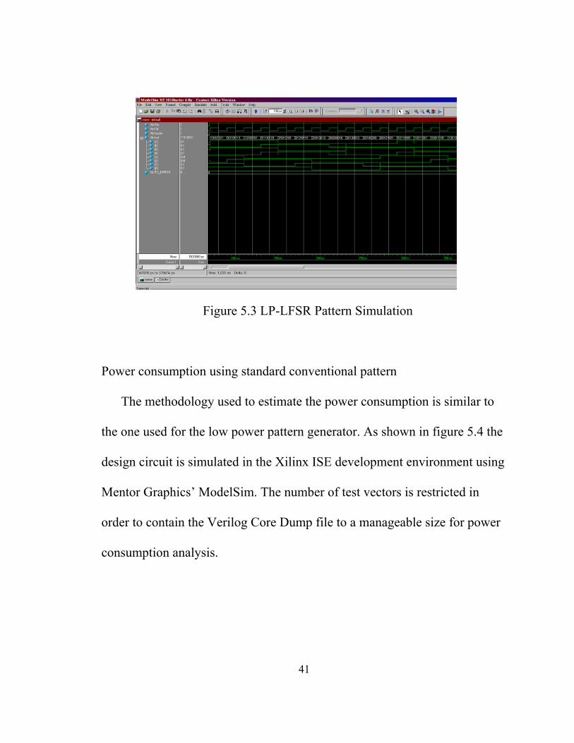
Figure 5.3 LP-LFSR Pattern Simulation
Power consumption using standard conventional pattern
The methodology used to estimate the power consumption is similar to
the one used for the low power pattern generator. As shown in figure 5.4 the
design circuit is simulated in the Xilinx ISE development environment using
Mentor Graphics’ ModelSim. The number of test vectors is restricted in
order to contain the Verilog Core Dump file to a manageable size for power
consumption analysis.
41

Fig 5.4 Power Estimation Flow
42

The VCD file contains the switching activity of the design circuit for the
number of test vectors. The number of test vectors is obtained from a Fault
simulation tool called TetraMax from Synopsys. This tool takes the VCD
file as the input file along with the c432 interrupt controller design file and
produces the number of test vectors required for the desired fault coverage.
Another way of generating specific number of vectors is by using the
clock period and simulation time. For instance if the clock period is 60ns
and the simulation time is 60us. The number of vectors produced will be
60us/60ns = 1000.
Using the standard pattern, the ATPG tool generates 330 vectors for
98% fault coverage which translates to approximately 16mw power
consumption by the c432 circuit.
Power consumption using low power pattern
The key to achieving Low power consumption in System-On-Chip
devices is by reducing the switching activity in the device under test. The
low power technique described in chapter 4 improves the correlation
between the signals of the successive vectors (i.e. input stimulus to the
43

circuit under test) resulting in reduced transitions of the primary inputs
hence reducing switching activity inside the circuit under test.
The methodology used in estimating the power consumption16,17 of
the device under test includes the generation of the 36-bit low power pattern,
synthesizing the c432 circuit using generic libraries, running the 36-bit
pattern on the c432 circuit and computing the power consumption using a
power estimation EDA tool.
Circuit Simulation is implemented using Mentor’s ModelSim tool in
the Xilinx ISE development environment. It is important to restrict the
simulation time (i.e. number of test vectors) to a few microseconds in order
to contain the VCD file to a manageable size for the purpose of evaluating
the switching activity. Xilinx xPower tool is used to read in the VCD file for
power consumption estimation. TetraMax was used to determine the number
of test vectors required for the desired fault coverage.
Power consumed by the c432 circuit is observed to be 10mw using
370 vectors for 98% fault coverage. Detailed reports on synthesis,
simulation and power estimation are included in Appendix C.
Power Consumption Comparison (Standard LFSR vs LP-LFSR)
44

Two test benches are designed using Verilog as labeled in Appendix B.
The first test bench uses a conventional test pattern generator and the
second test bench uses a low power pattern generator. Both test benches are
used to simulate a common design circuit which in this case is an industry
standard 27-channel interrupt controller benchmark circuit. Verilog code for
c432 is included in Appendix D.
Both test benches are designed to use the same pre-defined clock
period as well as identical simulation time. This ensures the same number of
test vectors generated by both test benches. The number of gates used by the
interrupt controller are 250 as indicated by the synthesis reports from the
Xilinx development environment. Logic gates used by the conventional test
bench are 60 and the number of gates used by the low power test bench are
135.
TetraMax ATPG and Fault simulation tool is used to estimate the
number of test vectors required for 98% fault coverage of the interrupt
controller. The tool generated 330 vectors for the conventional test bench
and 370 vectors for the low power test bench. Both test benches produced
almost the same number of test vectors for the desired fault coverage thus
demonstrating about the same test time used in both cases.
45

The two VCD files (for conventional and low power pattern)
containing the interrupt controller’s switching activity were used for power
consumption estimation by Xilinx xPower power analysis tool.
xPower calculates the average power consumed by the circuit for each
test vector applied by observing the logic value at each internal and external
node of the circuit. The transition in the logic value at each node (1 → 0 or 0
→ 1) results in the dynamic power consumption by the gate of the Xilinx
Spartan 2 device. Total power consumed by the circuit is the sum of the
power consumption by the circuit for each test vector.
The reported power consumption estimates as indicated above
demonstrates approximately 60% lower power consumption by the interrupt
controller using the low power test bench as compared with the conventional
pattern. This result demonstrates lower number of logic transitions at the
internal and external nodes of the test circuit. The difference in the power
consumption of the test logic between the two approaches (65 gates versus
135 gates is negligible).
46

Table 5.1 Power Consumption Comparison
Fault Coverage # of Test Vectors
# of Gates in the
Test Circuit
# of Gates in the Test
Controller Average Power Consumption
Conventional
The configurable logic blocks and input/output blocks used in most
field programmable gate arrays such as the Spartan 2 device are typically not
optimized for lowest power consumption compared with some options of the
gate array and Standard cell products. Therefore it is possible to achieve
even lower power consumption by the circuit in an ASIC implementation
compared with an FPGA.
Summary and Conclusion
The System on a chip revolution challenges both design and test
engineers especially in the area of power dissipation. Generally the chip
consumes more power in the manufacturing test mode than in normal
operation mode in its targeted system. The increase in the power
LFSR 0.98
330.00
250
65 16mW
LP-LPSR 0.98
370.00
250
130 10mW
47

consumption can result in un-repairable damages in the chip directly
impacting the overall yield and cost.
This thesis investigates the fundamental process used for IC Design, Test
and Manufacturing including design entry, tool flow methodology and hand-
off to Manufacturing. Specific detailed attention is focused on IC
verification and test.
Design-For-Test and Design-For-Manufacturing is the mainstream
approach today for IC Design. This approach is mandating the entire SOC
development team to collaborate very closely with each other in clearly
articulating adequate test requirements and methodology as well as ensuring
the manufacturability of the chip.
Various test methodologies such as external (ATE based), DFT-
SCAN/BIST and embedded (combination of low cost external tester and
SCAN/BIST) approaches are studied. The embedded approach is found to be
prevalent in SOC testing.
It may be easier, for the large Semiconductor component companies
when compared with smaller Fabless companies, to justify the cost of
expensive external ATE systems due to the higher utilization rate by the
48

former and inherent flexibility in expensive ATE’s to integrate test (e.g.
memory, mixed-signal, etc) specific electronics. Other trade-off factors
such as the impact of the number of pins required in the device for test,
external versus internal pattern generation, etc need to be carefully evaluated
for the most optimum cost versus performance test solution.
Including SCAN/BIST on the chip tends to increase the die size by a
small percentage and the power consumption of the chip. The increase in the
power consumption is attributed primarily to the increase in the circuit’s
switching activity. Random pattern generation theory is investigated along
with the correlation of the Linear Feedback Shift Register based PRPG,
matrix theory, characteristic polynomial and the generator polynomial.
A Technique to generate low power PRPG is implemented and
applied on an industry standard benchmark circuit for power consumption
estimation. The comparison of power consumption by the circuit
demonstrates 60% lower power consumed by the circuit when using low
power pattern as the input stimulus compared with the input stimulus
generated by the conventional LFSR based PRPG.
49
CHAPTER VI
RECOMMENDATIONS FOR FUTURE WORK
SOC designs are making a rapid shift from mostly digital to mixed
signal including millions of user defined logic gates and dozens of IP (Core
as well as I/O based). IC Verification and Test strategy needs to include
advanced controllers and pattern generators for testing digital as well as
analog components of the chip. Pattern generation inside the chip is well
known to cause increase in the power consumption of the IC during the
manufacturing test. New design and test techniques need to be investigated
to keep this increase in the power consumption by the chip as minimum as
possible.
The availability of advanced manufacturing process rules in the
design/verification libraries and tool flow methodologies is mandating the IC
front-end designers to verify the manufacturability of the chip much in
advance in the design process . Therefore development of the new SOC DFT
techniques needs to be compliant with the advanced DFM rules18.
50

SELECTED BIBLIOGRAPHY
1 1 Patrick Girard, “Survey of Low-Power Testing of VLSI Circuits, IEEE Design and Test of Computers, May-June 2002, Volume: 19 , Issue: 3, page(s): 80 – 90, ISSN: 0740-7475 2 2 S. Zhang, et. al, “Cost driven optimization of fault coverage in combined built-In-Self-Test/Automated Test Equipment Testing”, IEEE Instrumentation and Measurement Technology Conference, May 18-20, 2004 3 3 L. Ungar and T. Ambler, “Economics of Built-In-Self-Test”, IEEE Design and Test of Computers, Sept.-Oct. 2001, Volume: 18 , Issue: 5, page(s): 70 – 79, ISSN: 0740-7475 4 4 Benoit Nadeau-Dostie, “Design for AT-SPEED TEST, DIAGNOSIS and MESUREMENT, ISBN 0-7923-8669-8 5 5 T.Moon and W. Stirling, “ Mathematical Methods and Algorithms for Signal Processing”, ISBN 0-201-36186-8 6 6 A. J. van de Goor, “TESTING SEMICONDUCTOR MEMORIES theory and practice”, ISBN 90-80 4276-1-6 7 7 N.Ahmed, M. H. Tehranipour, M. Nourani, “Low Power Pattern Generation for BIST Architecture”, IEEE Circuits and Systems, 2004. ISCAS '04. Proceedings of the 2004 International Symposium, 23-26 May 2004, Vol. 2, pages 689-92 8 8 X. Zhang and K. Roy, “Peak Power reduction in low power BIST”, Quality Electronic Design, 2000. ISQED 2000. Proceedings. 20-22 March 2000, page(s): 425 – 432
51

9 9 G. Marsaglia and A. Zaman, “A New Class of Random Number Generators”, The annals of Applied Probability, 1991, Vol 1, No. 3, 462 – 480 10 10 G. Marsaglia and L. Tsay, “ Matrices and the Structure of Random Number Sequences”, Linear Algebra and its applications 67:147-156 (1985) 11 11 F. Nekoogar, “From ASICs to SOCs, A practical Approach”, ISBN 0-13-033857-5 12 12 Barabara Chappel, “The fine art of IC design”, IEEE Spectrum, July 1999, Volume: 36 , Issue: 7, page(s): 30 – 34, ISSN: 0018-9235 13 13 C. Wang and K. Roy, “Maximum Power Estimation for CMOS circuits using deterministic and statistic approaches”, 9th International conference on VLSI design, Jan 1996 14 14 E. Larson et, al, “Efficient Test Solutions for Core-Based Designs”, IEEE transactions on Computer aided design of integrated circuits and systems, vol. 23, May 2004 15 15 M.L. Mehta, “Some remarks on Random Number Generators”, Number theory and physics, 1990, Springer proceedings in Physics, Vol. 47, pages 253-259 16 16 F. Najm, “A survey of power estimation techniques in VLSI circuits”, IEEE Very Large Scale Integration (VLSI) Systems, Dec. 1994, Volume: 2 , Issue: 4, page(s): 446 – 455
52

17 17 F. Najm, “ Estimating power dissipation in VLSI circuits”, IEEE Circuits and Devices Magazine, July 1994, Volume: 10 , Issue: 4, page(s): 11 – 19 18 18 M. Schrader and R. McConnell, “SOC Design and Test considerations”, Design, Automation and Test in Europe Conference and Exhibition, 2003, page(s): 202 – 207, ISSN: 1530-1591
53

APPENDIX A
PATTERN GENERATION CONTROLLER
module top (Tte, Clk, resetn, out);
input Tte;
input Clk;
input resetn;
output [7:0] out;
wire En1;
wire En2;
wire Sel1;
wire Sel2;
wire anor;
wire [8:0] d;
//reg [8:0] q;
reg [8:5] q_upper;
reg [3:0] q_lower;
reg q_mid;
wire [7:0] out;
54

wire [7:0] qlfsr;
wire [7:0] dlfsr;
wire [7:0] rmuxout;
wire r;
lfsr_fsm lfsr_fsm_a
(.te(Tte), .clk(Clk), .en1(En1), .en2(En2), .sel1(Sel1), .sel2(Sel2));
always @(posedge En1 or negedge resetn)
begin
if (!resetn)
q_upper[8:5] <= 4'b0100;
else
q_upper[8:5] <= d[8:5];
end
always @(posedge En1 or negedge resetn)
begin
if (!resetn)
q_mid <= 1'b1;
else
q_mid <= d[4] ;
55

end
always @(posedge En2 or negedge resetn)
begin
if (!resetn)
q_lower[3:0] <= 4'b1011;
else
q_lower[3:0] <= d[3:0] ;
end
assign d[8:0] = {q_upper[8]^q_lower[0], q_upper[8:5], q_mid,
q_lower[3:1]};
//assign anor =
~(q_upper[8]|q_upper[7]|q_upper[6]|q_upper[5]|q_lower[3]|q_lower[2]|q_lo
wer[1]);
assign qlfsr = {q_upper[8:5],q_lower[3:0]};
assign dlfsr = {d[8:5],d[3:0]};
assign r = q_lower[0];
lfsr_andor_mux lfsr_andor_mux_a
(.qlfsr(qlfsr), .dlfsr(dlfsr), .r(r), .rmuxout(rmuxout));
assign out[7:4] = Sel1 ? q_upper[8:5] : rmuxout[7:4];
56
assign out[3:0] = Sel2 ? q_lower[3:0] : rmuxout[3:0];
endmodule
`timescale 1ns / 1ps
////////////////////////////////////////////////////////////////////////////////
// Company:
// Engineer:
// Create Date: 17:22:25 08/30/05
// Module Name: lfsr_andor_mux
// Revision 0.01 - File Created
// Additional Comments:
////////////////////////////////////////////////////////////////////////////////
module lfsr_andor_mux(qlfsr, dlfsr, r, rmuxout);
input [7:0] qlfsr;
input [7:0] dlfsr;
input r;
output [7:0] rmuxout;
wire [7:0] andout;
wire [7:0] orout;
assign andout[7:0] = qlfsr[7:0] & dlfsr[7:0];
57

assign orout[7:0] = qlfsr[7:0] | dlfsr[7:0];
assign rmuxout = r ? orout : andout;
endmodule
`timescale 1ns / 1ps
////////////////////////////////////////////////////////////////////////////////
// Module Name: lfsr_fsm
// Revision 0.01 - File Created
////////////////////////////////////////////////////////////////////////////////
module lfsr_fsm(te, clk, en1, en2, sel1, sel2);
input te;
input clk;
reg [2:0] count;
output en1;
output en2;
output sel1;
output sel2;
reg en1;
reg en2;
reg sel1;
58

reg sel2;
always @(posedge clk)
begin
if (te == 0)
count <= 3'b001;
else
count <= count + 1;
if (count >= 3'b100)
count <= 3'b001;
end
always @(posedge clk)
begin
if (te==1)
begin
if (count==3'b001)
begin
en1 <= 1'b1;
en2 <= 1'b0 ;
sel1 <= 1'b1 ;
59

sel2 <= 1'b1 ;
end
else if(count==3'b010)
begin
en1 <= 1'b0 ;
en2 <= 1'b0 ;
sel1 <= 1'b1 ;
sel2 <= 1'b0 ;
end
else if(count==3'b011)
begin
en1 <= 1'b0;
en2 <= 1'b1 ;
sel1 <= 1'b1;
sel2 <= 1'b1 ;
end
else if(count==3'b100)
begin
en1 <= 1'b0 ;
60

en2 <= 1'b0 ;
sel1 <= 1'b0;
sel2 <= 1'b1 ;
end
else
begin
en1 <= 1'b1;
en2 <= 1'b0 ;
sel1 <= 1'b1 ;
sel2 <= 1'b1 ;
end
end
end
endmodule
61

APPENDIX B
VERILOG TEST BENCH
`timescale 1ns / 1ps //////////////////////////////////////////////////////////////////////////////// // Company: // Engineer: // // Create Date: 17:08:47 12/08/2005 // Design Name: main // Module Name: testdec08.v // Project Name: projecta // Target Device: // Tool versions: // Description: // // Verilog Test Fixture created by ISE for module: main // // Dependencies: // // Revision: // Revision 0.01 - File Created // Additional Comments: // //////////////////////////////////////////////////////////////////////////////// module testdec08_v; // Inputs reg Clk; reg Reset; // Outputs
62

wire PA; wire PB; wire PC; wire [3:0] Chan; // Instantiate the Unit Under Test (UUT) main uut ( .PA(PA), .PB(PB), .PC(PC), .Chan(Chan), .Clk(Clk), .Reset(Reset) ); initial begin // Initialize Inputs Clk = 0; Reset = 0; // Wait 100 ns for global reset to finish #100; // Add stimulus here // Create a 60ns/16.7MHZ clock and run it for a few us Reset = 1; end always #30 Clk = ~ Clk; //Need to set sim time in modelsim for the VCD file - try atleast 6us // for sufficient switching activity. For 6us VCD file size is 26KB
63

initial begin $dumpfile ("conv.vcd") ; $dumpvars(1, testdec08_v.uut); end endmodule module conv36(clk, resetn, lout); input clk; input resetn; output [35:0] lout; wire znor,znor1,znor2; wire [35:0] d; reg [35:0] q; always @(posedge clk or negedge resetn) begin if (!resetn) q <= 36'H000000000; else q <= d; end assign d[35:0] = {q[35]^q[24]^znor,q[35:1]}; assign lout[35:0] = q[35:0]; assign znor1 = ~|q[23:0]; assign znor2 = ~|q[34:24]; assign znor = znor1&znor2; endmodule
64
`timescale 1ns / 1ps //////////////////////////////////////////////////////////////////////////////// // Company: // Engineer: // // Create Date: 13:29:29 11/01/05 // Design Name: // Module Name: lfsr36top // Project Name: // Target Device: // Tool versions: // Description: // // Dependencies: // // Revision: // Revision 0.01 - File Created // Additional Comments: // //////////////////////////////////////////////////////////////////////////////// module modpatt_v; // Inputs reg Clk; reg Reset; reg TE; // Outputs wire PA; wire PB; wire PC; wire [3:0] Chan; // Instantiate the Unit Under Test (UUT) main uut (
65
.PA(PA), .PB(PB), .PC(PC), .Chan(Chan), .Clk(Clk), .Reset(Reset), .TE(TE) ); initial begin // Initialize Inputs Clk = 0; Reset = 0; TE = 0; // Wait 100 ns for global reset to finish #100; // Add stimulus here Reset = 1; TE = 1; end //Clock is 16.7MHZ (60ns), simulate in modelsim for 6us for the VCD file always #30 Clk = ~ Clk; initial begin $dumpfile ("mod.vcd"); $dumpvars(1, modpatt_v.uut);
66

end endmodule `
67

APPENDIX C
XILINX REPORTS
TABLE OF CONTENTS
1) Synthesis Options Summary
2) HDL Compilation
3) HDL Analysis
4) HDL Synthesis
5) Advanced HDL Synthesis
5.1) HDL Synthesis Report
6) Low Level Synthesis
7) Final Report
7.1) Device utilization summary
* Synthesis Options Summary *
---- Source Parameters
Input File Name : "top.prj"
Input Format : mixed
Ignore Synthesis Constraint File : NO
---- Target Parameters
68

Output File Name : "top"
Output Format : NGC
Target Device : xc2s200-6-pq208
---- Source Options
Top Module Name : top
Automatic FSM Extraction : YES
FSM Encoding Algorithm : Auto
FSM Style : lut
RAM Extraction : Yes
RAM Style : Auto
ROM Extraction : Yes
ROM Style : Auto
Mux Extraction : YES
Mux Style : Auto
Decoder Extraction : YES
Priority Encoder Extraction : YES
Shift Register Extraction : YES
Logical Shifter Extraction : YES
XOR Collapsing : YES
69
Resource Sharing : YES
Multiplier Style : lut
Automatic Register Balancing : No
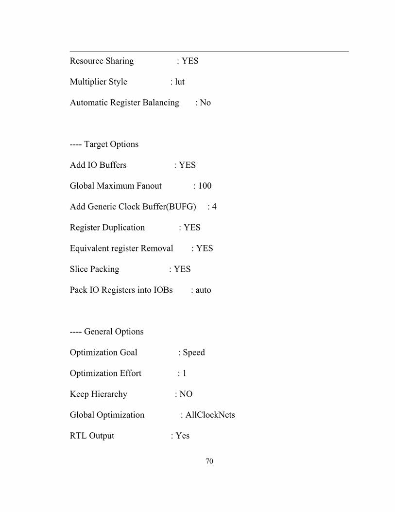
---- Target Options
Add IO Buffers : YES
Global Maximum Fanout : 100
Add Generic Clock Buffer(BUFG) : 4
Register Duplication : YES
Equivalent register Removal : YES
Slice Packing : YES
Pack IO Registers into IOBs : auto
---- General Options
Optimization Goal : Speed
Optimization Effort : 1
Keep Hierarchy : NO
Global Optimization : AllClockNets
RTL Output : Yes
70

Write Timing Constraints : NO
Hierarchy Separator : /
Bus Delimiter : <>
Case Specifier : maintain
Slice Utilization Ratio : 100
Slice Utilization Ratio Delta : 5
---- Other Options
lso : top.lso
Read Cores : YES
cross_clock_analysis : NO
verilog2001 : YES
safe_implementation : No
Optimize Instantiated Primitives : NO
tristate2logic : Yes
use_clock_enable : Yes
use_sync_set : Yes
use_sync_reset : Yes
enable_auto_floorplanning : No
71

======================================================
===================
* HDL Compilation *
Compiling verilog file "lfsr_fsm.v"
Module <lfsr_fsm> compiled
Compiling verilog file "lfsr_andor_mux.v"
Module <lfsr_andor_mux> compiled
Compiling verilog file "top.v"
Module <top> compiled
No errors in compilation
Analysis of file <"top.prj"> succeeded.
* HDL Analysis *
Analyzing top module <top>.
Module <top> is correct for synthesis.
Set property "resynthesize = true" for unit <top>.
Analyzing module <lfsr_fsm>.
72

Module <lfsr_fsm> is correct for synthesis.
Analyzing module <lfsr_andor_mux>.
Module <lfsr_andor_mux> is correct for synthesis.
* HDL Synthesis *
Synthesizing Unit <lfsr_andor_mux>.
Related source file is "lfsr_andor_mux.v".
Unit <lfsr_andor_mux> synthesized.
Synthesizing Unit <lfsr_fsm>.
Related source file is "lfsr_fsm.v".
Found 1-bit register for signal <en1>.
Found 1-bit register for signal <en2>.
Found 1-bit register for signal <sel1>.
Found 1-bit register for signal <sel2>.
Found 3-bit comparator greatequal for signal <$n0000> created at line 54.
73

Found 3-bit up counter for signal <count>.
Summary:
inferred 1 Counter(s).
inferred 4 D-type flip-flop(s).
inferred 1 Comparator(s).
Unit <lfsr_fsm> synthesized.
Synthesizing Unit <top>.
Related source file is "top.v".
WARNING:Xst:1780 - Signal <anor> is never used or assigned.
Found 1-bit xor2 for signal <$n0000> created at line 92.
Found 4-bit register for signal <q_lower>.
Found 1-bit register for signal <q_mid>.
Found 4-bit register for signal <q_upper>.
Summary:
inferred 1 D-type flip-flop(s).
Unit <top> synthesized.
* Advanced HDL Synthesis *
74

=================================================
Advanced RAM inference ...
Advanced multiplier inference ...
Advanced Registered AddSub inference ...
Dynamic shift register inference ...
HDL Synthesis Report
Macro Statistics
# Counters : 1
3-bit up counter : 1
# Registers : 7
1-bit register : 5
4-bit register : 2
# Comparators : 1
3-bit comparator greatequal : 1
# Xors : 1
1-bit xor2 : 1
75

* Low Level Synthesis *
Optimizing unit <top> ...
Optimizing unit <lfsr_fsm> ...
Optimizing unit <lfsr_andor_mux> ...
Loading device for application Rf_Device from file 'v200.nph' in
environment C:/Xilinx.
Mapping all equations...
Building and optimizing final netlist ...
Found area constraint ratio of 100 (+ 5) on block top, actual ratio is 0.
* Final Report *
Final Results
RTL Top Level Output File Name : top.ngr
Top Level Output File Name : top
Output Format : NGC
Optimization Goal : Speed
Keep Hierarchy : NO
76

Design Statistics
# IOs : 11
Macro Statistics :
# Registers : 17
# 1-bit register : 17
# Comparators : 1
# 3-bit comparator greatequal : 1
Cell Usage :
# BELS : 16
# INV : 1
# LUT2_L : 2
# LUT3 : 1
# LUT3_L : 5
# LUT4 : 6
# LUT4_L : 1
# FlipFlops/Latches : 16
# FDC : 4
# FDE : 4
# FDP : 5
77

# FDR : 2
# FDS : 1
# Clock Buffers : 1
# BUFGP : 1
# IO Buffers : 10
# IBUF : 2
# OBUF : 8
Device utilization summary:
---------------------------
Selected Device : 2s200pq208-6
Number of Slices: 9 out of 2352 0%
Number of Slice Flip Flops: 16 out of 4704 0%
Number of 4 input LUTs: 15 out of 4704 0%
Number of bonded IOBs: 11 out of 144 7%
Number of GCLKs: 1 out of 4 25%
78

Total memory usage is 86756 kilobytes
Number of errors : 0 ( 0 filtered)
Number of warnings : 1 ( 0 filtered)
Number of infos : 1 ( 0 filtered)
Release 7.1.02i - XPower SoftwareVersion:H.40 Copyright (c) 1995-2005 Xilinx, Inc. All rights reserved. Design: main.ncd Preferences: main.pcf VCD File: C:\Xilinx\bin\Design with inputs from low power lfsr\mod.vcd Part: 2s200pq208-6 Data version: PRELIMINARY,v1.0,07-31-02 XPower and Datasheet may have some Quiescent Current differences. This is due to the fact that the quiescent numbers in XPower are based on measurements of real designs with active functional elements reflecting real world design scenarios. Power summary: I(mA) P(mW) ---------------------------------------------------------------- Total estimated power consumption: 10 --- Vccint 2.50V: 1 2 Vcco33 3.30V: 2 8 --- Clocks: 0 0 Inputs: 1 2 Logic: 0 1 Outputs:
79
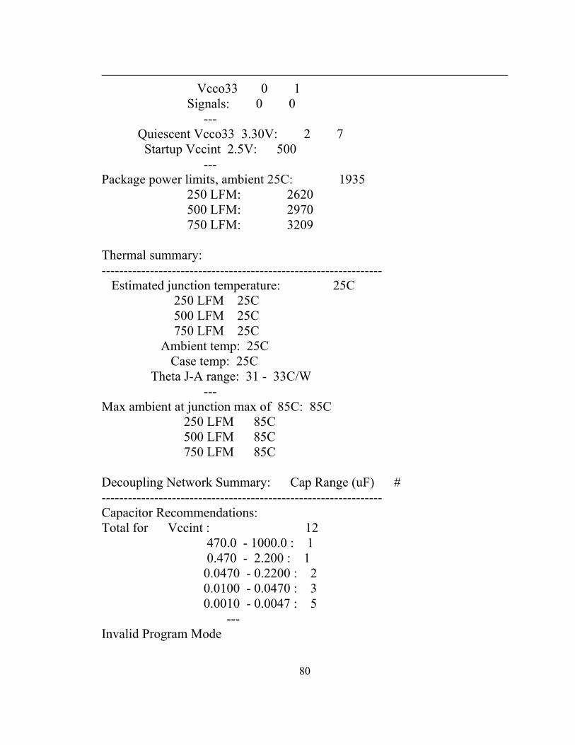
Vcco33 0 1 Signals: 0 0 --- Quiescent Vcco33 3.30V: 2 7 Startup Vccint 2.5V: 500 --- Package power limits, ambient 25C: 1935 250 LFM: 2620 500 LFM: 2970 750 LFM: 3209 Thermal summary: ---------------------------------------------------------------- Estimated junction temperature: 25C 250 LFM 25C 500 LFM 25C 750 LFM 25C Ambient temp: 25C Case temp: 25C Theta J-A range: 31 - 33C/W --- Max ambient at junction max of 85C: 85C 250 LFM 85C 500 LFM 85C 750 LFM 85C Decoupling Network Summary: Cap Range (uF) # ---------------------------------------------------------------- Capacitor Recommendations: Total for Vccint : 12 470.0 - 1000.0 : 1 0.470 - 2.200 : 1 0.0470 - 0.2200 : 2 0.0100 - 0.0470 : 3 0.0010 - 0.0047 : 5 --- Invalid Program Mode
80

Total for Vcco33 : 8 470.0 - 1000.0 : 1 0.0470 - 0.2200 : 1 0.0100 - 0.0470 : 2 0.0010 - 0.0047 : 4 Power details: ------------------------------------------------------------------------------- Inputs: Loads Loading(fF) C(pF) F(MHz) I(mA) P(mW) ------------------------------------------------------------------------------- Clk_BUFGP/IBUFG 16000 16.7 0.7 1.7 Reset_IBUF 2970 0.1 0.0 0.0 TE_IBUF 2970 0.1 0.0 0.0 ------------------------------------------------------------------------------- Outputs:1 Loads Loading(fF) C(pF) F(MHz) I(mA) P(mW) ------------------------------------------------------------------------------- Vcco33 PC_OBUF 35000 13 0.7 0.1 0.3 Chan_0_OBUF 35000 13 0.3 0.0 0.1 Chan_2_OBUF 35000 13 0.3 0.0 0.1 PB_OBUF 35000 13 0.3 0.0 0.1 Chan_1_OBUF 35000 13 0.2 0.0 0.1 Chan_3_OBUF 35000 13 0.1 0.0 0.0 PA_OBUF 35000 13 0.1 0.0 0.0 ------------------------------------------------------------------------------- Logic: Loads Loading(fF) C(pF) F(MHz) I(mA) P(mW) ------------------------------------------------------------------------------- sr2/_n00631 2400 0.9 0.0 0.0 sr2/_n00661 2400 0.9 0.0 0.0 M3/PC384_SW1_SW0 2400 0.8 0.0 0.0 M3/PC622_SW0 2400 0.8 0.0 0.0 sr2/_n00841 2400 0.8 0.0 0.0 sr2/_n00871 2400 0.8 0.0 0.0 sr2/_n00901 2400 0.8 0.0 0.0 M3/PC104 2400 0.7 0.0 0.0 M3/PC252_SW0 2400 0.7 0.0 0.0 M3/PC252_SW1 2400 0.7 0.0 0.0
81
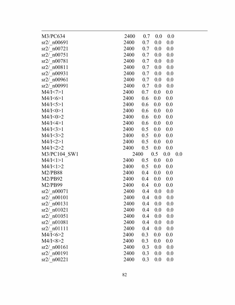
M3/PC634 2400 0.7 0.0 0.0 sr2/_n00691 2400 0.7 0.0 0.0 sr2/_n00721 2400 0.7 0.0 0.0 sr2/_n00751 2400 0.7 0.0 0.0 sr2/_n00781 2400 0.7 0.0 0.0 sr2/_n00811 2400 0.7 0.0 0.0 sr2/_n00931 2400 0.7 0.0 0.0 sr2/_n00961 2400 0.7 0.0 0.0 sr2/_n00991 2400 0.7 0.0 0.0 M4/I<7>1 2400 0.7 0.0 0.0 M4/I<6>1 2400 0.6 0.0 0.0 M4/I<5>1 2400 0.6 0.0 0.0 M4/I<0>1 2400 0.6 0.0 0.0 M4/I<0>2 2400 0.6 0.0 0.0 M4/I<4>1 2400 0.6 0.0 0.0 M4/I<3>1 2400 0.5 0.0 0.0 M4/I<3>2 2400 0.5 0.0 0.0 M4/I<2>1 2400 0.5 0.0 0.0 M4/I<2>2 2400 0.5 0.0 0.0 M3/PC104_SW1 2400 0.5 0.0 0.0 M4/I<1>1 2400 0.5 0.0 0.0 M4/I<1>2 2400 0.5 0.0 0.0 M2/PB88 2400 0.4 0.0 0.0 M2/PB92 2400 0.4 0.0 0.0 M2/PB99 2400 0.4 0.0 0.0 sr2/_n00071 2400 0.4 0.0 0.0 sr2/_n00101 2400 0.4 0.0 0.0 sr2/_n00131 2400 0.4 0.0 0.0 sr2/_n01021 2400 0.4 0.0 0.0 sr2/_n01051 2400 0.4 0.0 0.0 sr2/_n01081 2400 0.4 0.0 0.0 sr2/_n01111 2400 0.4 0.0 0.0 M4/I<6>2 2400 0.3 0.0 0.0 M4/I<8>2 2400 0.3 0.0 0.0 sr2/_n00161 2400 0.3 0.0 0.0 sr2/_n00191 2400 0.3 0.0 0.0 sr2/_n00221 2400 0.3 0.0 0.0
82
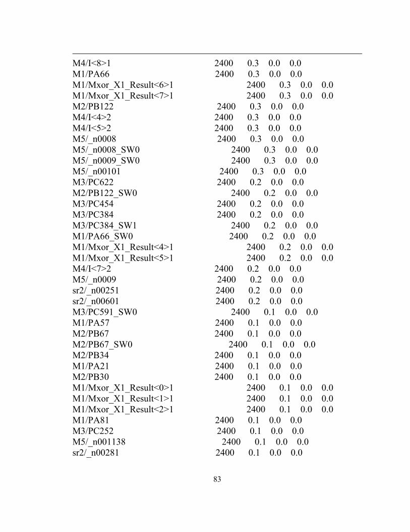
M4/I<8>1 2400 0.3 0.0 0.0 M1/PA66 2400 0.3 0.0 0.0 M1/Mxor_X1_Result<6>1 2400 0.3 0.0 0.0 M1/Mxor_X1_Result<7>1 2400 0.3 0.0 0.0 M2/PB122 2400 0.3 0.0 0.0 M4/I<4>2 2400 0.3 0.0 0.0 M4/I<5>2 2400 0.3 0.0 0.0 M5/_n0008 2400 0.3 0.0 0.0 M5/_n0008_SW0 2400 0.3 0.0 0.0 M5/_n0009_SW0 2400 0.3 0.0 0.0 M5/_n00101 2400 0.3 0.0 0.0 M3/PC622 2400 0.2 0.0 0.0 M2/PB122_SW0 2400 0.2 0.0 0.0 M3/PC454 2400 0.2 0.0 0.0 M3/PC384 2400 0.2 0.0 0.0 M3/PC384_SW1 2400 0.2 0.0 0.0 M1/PA66_SW0 2400 0.2 0.0 0.0 M1/Mxor_X1_Result<4>1 2400 0.2 0.0 0.0 M1/Mxor_X1_Result<5>1 2400 0.2 0.0 0.0 M4/I<7>2 2400 0.2 0.0 0.0 M5/_n0009 2400 0.2 0.0 0.0 sr2/_n00251 2400 0.2 0.0 0.0 sr2/_n00601 2400 0.2 0.0 0.0 M3/PC591_SW0 2400 0.1 0.0 0.0 M1/PA57 2400 0.1 0.0 0.0 M2/PB67 2400 0.1 0.0 0.0 M2/PB67_SW0 2400 0.1 0.0 0.0 M2/PB34 2400 0.1 0.0 0.0 M1/PA21 2400 0.1 0.0 0.0 M2/PB30 2400 0.1 0.0 0.0 M1/Mxor_X1_Result<0>1 2400 0.1 0.0 0.0 M1/Mxor_X1_Result<1>1 2400 0.1 0.0 0.0 M1/Mxor_X1_Result<2>1 2400 0.1 0.0 0.0 M1/PA81 2400 0.1 0.0 0.0 M3/PC252 2400 0.1 0.0 0.0 M5/_n001138 2400 0.1 0.0 0.0 sr2/_n00281 2400 0.1 0.0 0.0
83

sr2/_n00311 2400 0.1 0.0 0.0 sr2/_n00341 2400 0.1 0.0 0.0 sr2/_n00371 2400 0.1 0.0 0.0 sr2/_n00401 2400 0.1 0.0 0.0 sr2/_n00431 2400 0.1 0.0 0.0 sr2/_n00461 2400 0.1 0.0 0.0 sr2/lfsr_fsm_a/count__n0001<0>1 2400 0.1 0.0 0.0 sr2/lfsr_fsm_a/count__n0001<1>1 2400 0.1 0.0 0.0 sr2/lfsr_fsm_a/count__n0001<2>1 2400 0.1 0.0 0.0 M1/PA10 2400 0.1 0.0 0.0 M3/PC591_SW1 2400 0.1 0.0 0.0 M3/PC606 2400 0.0 0.0 0.0 M3/PC268_SW0 2400 0.0 0.0 0.0 M2/PB11 2400 0.0 0.0 0.0 M3/PC591 2400 0.0 0.0 0.0 M3/PC268 2400 0.0 0.0 0.0 Clk_BUFGP/BUFG.CE_POWER 0 0.0 0.0 0.0 M5/_n001112 2400 0.0 0.0 0.0 sr2/Mxor__n0000_Result1 2400 0.0 0.0 0.0 sr2/_n00491 2400 0.0 0.0 0.0 sr2/_n00521 2400 0.0 0.0 0.0 sr2/_n00551 2400 0.0 0.0 0.0 sr2/lfsr_fsm_a/_n00011 2400 0.0 0.0 0.0 sr2/lfsr_fsm_a/_n00021 2400 0.0 0.0 0.0 sr2/lfsr_fsm_a/_n00031 2400 0.0 0.0 0.0 sr2/lfsr_fsm_a/_n00041 2400 0.0 0.0 0.0 sr2/lfsr_fsm_a/count_0 275 0.0 0.0 0.0 sr2/lfsr_fsm_a/count_1 275 0.0 0.0 0.0 sr2/lfsr_fsm_a/count_2 275 0.0 0.0 0.0 sr2/lfsr_fsm_a/en1 275 0.0 0.0 0.0 sr2/lfsr_fsm_a/en2 275 0.0 0.0 0.0 sr2/lfsr_fsm_a/sel1 275 0.0 0.0 0.0 sr2/lfsr_fsm_a/sel2 275 0.0 0.0 0.0 sr2/q_lower_0 275 0.0 0.0 0.0 sr2/q_lower_1 275 0.0 0.0 0.0 sr2/q_lower_10 275 0.0 0.0 0.0 sr2/q_lower_11 275 0.0 0.0 0.0
84

sr2/q_lower_12 275 0.0 0.0 0.0 sr2/q_lower_13 275 0.0 0.0 0.0 sr2/q_lower_14 275 0.0 0.0 0.0 sr2/q_lower_15 275 0.0 0.0 0.0 sr2/q_lower_16 275 0.0 0.0 0.0 sr2/q_lower_17 275 0.0 0.0 0.0 sr2/q_lower_2 275 0.0 0.0 0.0 sr2/q_lower_3 275 0.0 0.0 0.0 sr2/q_lower_4 275 0.0 0.0 0.0 sr2/q_lower_5 275 0.0 0.0 0.0 sr2/q_lower_6 275 0.0 0.0 0.0 sr2/q_lower_7 275 0.0 0.0 0.0 sr2/q_lower_8 275 0.0 0.0 0.0 sr2/q_lower_9 275 0.0 0.0 0.0 sr2/q_mid 275 0.0 0.0 0.0 sr2/q_upper_0 275 0.0 0.0 0.0 sr2/q_upper_1 275 0.0 0.0 0.0 sr2/q_upper_10 275 0.0 0.0 0.0 sr2/q_upper_11 275 0.0 0.0 0.0 sr2/q_upper_12 275 0.0 0.0 0.0 sr2/q_upper_13 275 0.0 0.0 0.0 sr2/q_upper_14 275 0.0 0.0 0.0 sr2/q_upper_15 275 0.0 0.0 0.0 sr2/q_upper_16 275 0.0 0.0 0.0 sr2/q_upper_16.BY0 0 0.0 0.0 0.0 sr2/q_upper_17 275 0.0 0.0 0.0 sr2/q_upper_2 275 0.0 0.0 0.0 sr2/q_upper_3 275 0.0 0.0 0.0 sr2/q_upper_4 275 0.0 0.0 0.0 sr2/q_upper_5 275 0.0 0.0 0.0 sr2/q_upper_6 275 0.0 0.0 0.0 sr2/q_upper_7 275 0.0 0.0 0.0 sr2/q_upper_8 275 0.0 0.0 0.0 sr2/q_upper_9 275 0.0 0.0 0.0 ------------------------------------------------------------------------------- Signals: Loads Loading(fF) C(pF) F(MHz) I(mA) P(mW) -------------------------------------------------------------------------------
85

PC_OBUF 0 4 0.7 0.0 ~0.0 PB_OBUF 0 8 0.3 0.0 ~0.0 Reset_IBUF 0 14 0.1 0.0 0.0 srBus<24> 0 1 0.7 0.0 ~0.0 srBus<22> 0 1 0.7 0.0 ~0.0 srBus<20> 0 1 0.4 0.0 ~0.0 PA_OBUF 0 8 0.1 0.0 0.0 srBus<34> 0 0 0.9 0.0 ~0.0 srBus<12> 0 1 0.3 0.0 ~0.0 srBus<14> 0 1 0.3 0.0 ~0.0 srBus<17> 0 1 0.4 0.0 ~0.0 srBus<13> 0 1 0.3 0.0 ~0.0 srBus<16> 0 1 0.4 0.0 ~0.0 srBus<33> 0 0 0.9 0.0 ~0.0 srBus<30> 0 0 0.7 0.0 ~0.0 srBus<18> 0 0 0.4 0.0 ~0.0 srBus<25> 0 0 0.8 0.0 ~0.0 Chan_0_OBUF 0 1 0.3 0.0 ~0.0 N573 0 0 0.8 0.0 ~0.0 srBus<15> 0 0 0.4 0.0 ~0.0 Chan_1_OBUF 0 1 0.2 0.0 ~0.0 I<8> 0 0 0.3 0.0 ~0.0 I<4> 0 1 0.3 0.0 ~0.0 srBus<19> 0 0 0.4 0.0 ~0.0 Chan_2_OBUF 0 1 0.3 0.0 ~0.0 I<7> 0 1 0.2 0.0 ~0.0 X1<4> 0 1 0.2 0.0 ~0.0 I<5> 0 0 0.3 0.0 ~0.0 I<6> 0 0 0.3 0.0 ~0.0 srBus<5> 0 2 0.1 0.0 0.0 srBus<21> 0 0 0.4 0.0 ~0.0 srBus<11> 0 1 0.2 0.0 ~0.0 X1<6> 0 0 0.3 0.0 ~0.0 srBus<10> 0 1 0.1 0.0 0.0 X1<0> 0 1 0.1 0.0 0.0 srBus<28> 0 0 0.7 0.0 ~0.0 srBus<4> 0 1 0.1 0.0 0.0
86

M4/N4 0 0 0.5 0.0 ~0.0 srBus<7> 0 1 0.1 0.0 0.0 srBus<6> 0 1 0.1 0.0 0.0 srBus<9> 0 1 0.1 0.0 0.0 X1<2> 0 1 0.1 0.0 0.0 srBus<8> 0 1 0.1 0.0 0.0 CHOICE932 0 0 0.2 0.0 ~0.0 CHOICE788 0 1 0.1 0.0 ~0.0 Chan_3_OBUF 0 1 0.1 0.0 0.0 X1<7> 0 0 0.3 0.0 ~0.0 X1<1> 0 1 0.1 0.0 0.0 N555 0 0 0.2 0.0 ~0.0 CHOICE783 0 1 0.1 0.0 0.0 X1<5> 0 0 0.2 0.0 ~0.0 srBus<35> 0 0 0.2 0.0 ~0.0 CHOICE801 0 0 0.1 0.0 ~0.0 N559 0 0 0.1 0.0 ~0.0 CHOICE817 0 0 0.1 0.0 0.0 CHOICE818 0 0 0.1 0.0 ~0.0 N569 0 0 0.0 0.0 0.0 CHOICE980 0 0 0.0 0.0 0.0 CHOICE810 0 0 0.0 0.0 0.0 N567 0 0 0.1 0.0 0.0 CHOICE902 0 0 0.0 0.0 0.0 CHOICE769 0 0 0.0 0.0 0.0 CHOICE803 0 0 0.3 0.0 ~0.0 CHOICE826 0 0 0.1 0.0 ~0.0 CHOICE835 0 0 0.0 0.0 0.0 CHOICE836 0 0 0.0 0.0 0.0 CHOICE837 0 0 0.0 0.0 0.0 CHOICE869 0 0 0.0 0.0 0.0 CHOICE901 0 0 0.0 0.0 0.0 CHOICE945 0 0 0.2 0.0 ~0.0 CHOICE979 0 0 0.0 0.0 0.0 CHOICE981 0 0 0.2 0.0 ~0.0 I<0> 0 0 0.0 0.0 0.0 I<1> 0 0 0.0 0.0 0.0
87

I<2> 0 1 0.0 0.0 0.0 I<3> 0 1 0.0 0.0 0.0 M4/N0 0 0 0.3 0.0 ~0.0 M4/N10 0 0 0.5 0.0 ~0.0 M4/N12 0 0 0.6 0.0 ~0.0 M4/N14 0 0 0.7 0.0 ~0.0 M4/N16 0 0 0.6 0.0 ~0.0 M4/N2 0 0 0.6 0.0 ~0.0 M4/N6 0 0 0.5 0.0 ~0.0 M4/N8 0 0 0.6 0.0 ~0.0 N11 0 0 0.0 0.0 0.0 N547 0 0 0.1 0.0 ~0.0 N549 0 0 0.0 0.0 0.0 N557 0 0 0.2 0.0 ~0.0 N561 0 0 0.0 0.0 0.0 N563 0 0 0.0 0.0 0.0 N565 0 0 0.5 0.0 ~0.0 N571 0 0 0.2 0.0 ~0.0 N9 0 0 0.0 0.0 0.0 sr2/d<35> 0 0 0.0 0.0 0.0 sr2/lfsr_fsm_a/count<0> 0 2 0.0 0.0 0.0 sr2/lfsr_fsm_a/count<1> 0 2 0.0 0.0 0.0 sr2/lfsr_fsm_a/count<2> 0 3 0.0 0.0 0.0 sr2/lfsr_fsm_a/en1 0 9 0.0 0.0 0.0 sr2/lfsr_fsm_a/en2 0 9 0.0 0.0 0.0 sr2/lfsr_fsm_a/sel1 0 6 0.0 0.0 0.0 sr2/lfsr_fsm_a/sel2 0 6 0.0 0.0 0.0 sr2/q_lower<0> 0 12 0.0 0.0 0.0 sr2/q_lower<10> 0 1 0.0 0.0 0.0 sr2/q_lower<11> 0 1 0.0 0.0 0.0 sr2/q_lower<12> 0 1 0.0 0.0 0.0 sr2/q_lower<13> 0 1 0.0 0.0 0.0 sr2/q_lower<14> 0 1 0.0 0.0 0.0 sr2/q_lower<15> 0 1 0.0 0.0 0.0 sr2/q_lower<16> 0 1 0.0 0.0 0.0 sr2/q_lower<17> 0 1 0.0 0.0 0.0 sr2/q_lower<1> 0 1 0.0 0.0 0.0
88

sr2/q_lower<2> 0 1 0.0 0.0 0.0 sr2/q_lower<3> 0 1 0.0 0.0 0.0 sr2/q_lower<4> 0 2 0.0 0.0 0.0 sr2/q_lower<5> 0 1 0.0 0.0 0.0 sr2/q_lower<6> 0 1 0.0 0.0 0.0 sr2/q_lower<7> 0 1 0.0 0.0 0.0 sr2/q_lower<8> 0 1 0.0 0.0 0.0 sr2/q_lower<9> 0 1 0.0 0.0 0.0 sr2/q_mid 0 1 0.0 0.0 0.0 sr2/q_upper_0 0 1 0.0 0.0 0.0 sr2/q_upper_1 0 1 0.0 0.0 0.0 sr2/q_upper_10 0 1 0.0 0.0 0.0 sr2/q_upper_11 0 1 0.0 0.0 0.0 sr2/q_upper_12 0 1 0.0 0.0 0.0 sr2/q_upper_13 0 1 0.0 0.0 0.0 sr2/q_upper_14 0 2 0.0 0.0 0.0 sr2/q_upper_15 0 1 0.0 0.0 0.0 sr2/q_upper_16 0 1 0.0 0.0 0.0 sr2/q_upper_17 0 2 0.0 0.0 0.0 sr2/q_upper_2 0 1 0.0 0.0 0.0 sr2/q_upper_3 0 1 0.0 0.0 0.0 sr2/q_upper_4 0 1 0.0 0.0 0.0 sr2/q_upper_5 0 1 0.0 0.0 0.0 sr2/q_upper_6 0 2 0.0 0.0 0.0 sr2/q_upper_7 0 1 0.0 0.0 0.0 sr2/q_upper_8 0 1 0.0 0.0 0.0 sr2/q_upper_9 0 1 0.0 0.0 0.0 srBus<1> 0 2 0.0 0.0 0.0 srBus<23> 0 0 0.7 0.0 ~0.0 srBus<26> 0 0 0.8 0.0 ~0.0 srBus<27> 0 0 0.8 0.0 ~0.0 srBus<29> 0 0 0.7 0.0 ~0.0 srBus<2> 0 1 0.0 0.0 0.0 srBus<31> 0 0 0.7 0.0 ~0.0 srBus<32> 0 0 0.7 0.0 ~0.0 srBus<3> 0 2 0.0 0.0 0.0 -------------------------------------------------------------------------------
89
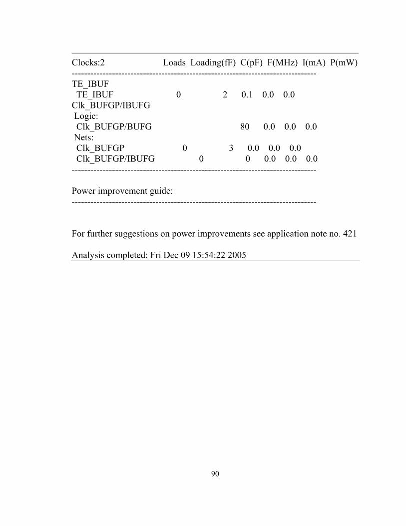
Clocks:2 Loads Loading(fF) C(pF) F(MHz) I(mA) P(mW) ------------------------------------------------------------------------------- TE_IBUF TE_IBUF 0 2 0.1 0.0 0.0 Clk_BUFGP/IBUFG Logic: Clk_BUFGP/BUFG 80 0.0 0.0 0.0 Nets: Clk_BUFGP 0 3 0.0 0.0 0.0 Clk_BUFGP/IBUFG 0 0 0.0 0.0 0.0 ------------------------------------------------------------------------------- Power improvement guide: ------------------------------------------------------------------------------- For further suggestions on power improvements see application note no. 421 Analysis completed: Fri Dec 09 15:54:22 2005
90
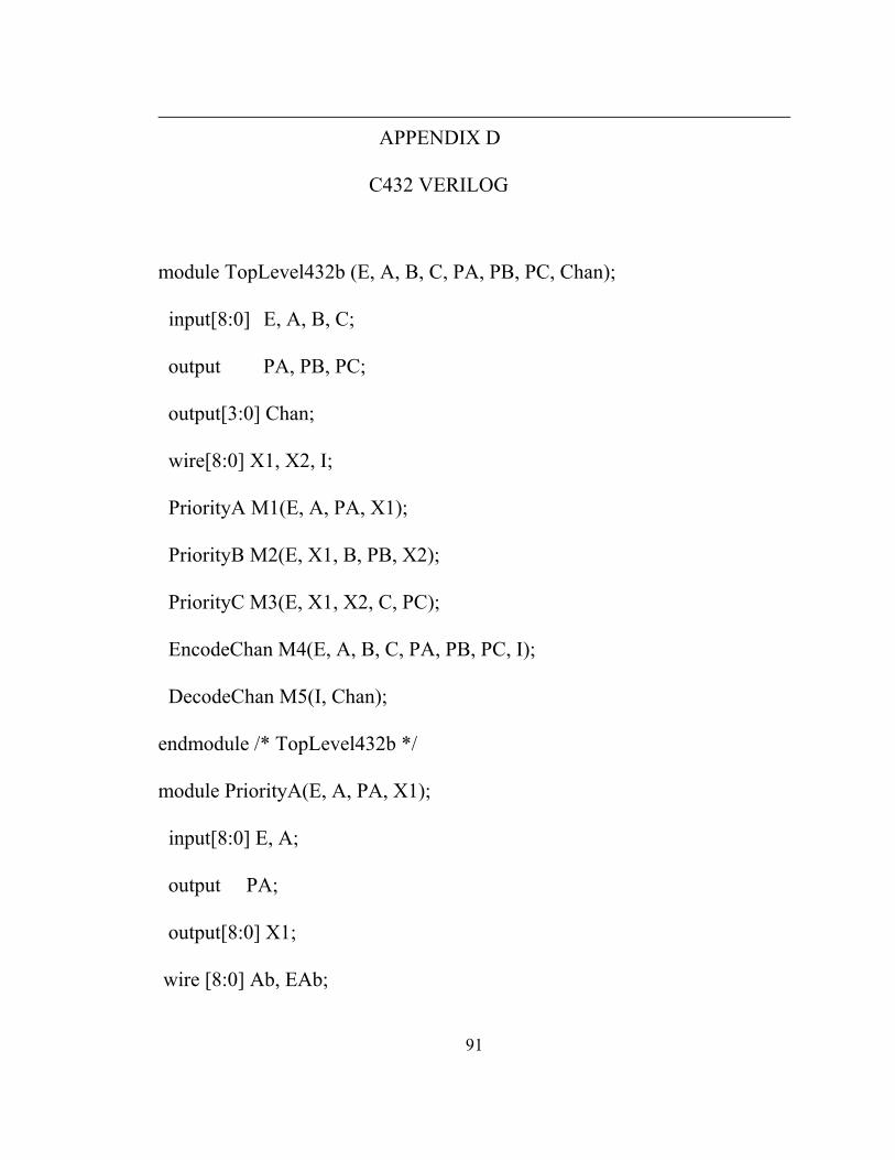
APPENDIX D
C432 VERILOG
module TopLevel432b (E, A, B, C, PA, PB, PC, Chan);
input[8:0] E, A, B, C;
output PA, PB, PC;
output[3:0] Chan;
wire[8:0] X1, X2, I;
PriorityA M1(E, A, PA, X1);
PriorityB M2(E, X1, B, PB, X2);
PriorityC M3(E, X1, X2, C, PC);
EncodeChan M4(E, A, B, C, PA, PB, PC, I);
DecodeChan M5(I, Chan);
endmodule /* TopLevel432b */
module PriorityA(E, A, PA, X1);
input[8:0] E, A;
output PA;
output[8:0] X1;
wire [8:0] Ab, EAb;
91

assign Ab = ~A;
assign EAb = ~(Ab & E);
assign PA = ~&EAb;
assign X1 = EAb ^ {9{PA}};
endmodule /* PriorityA */
module PriorityB(E, X1, B, PB, X2);
input[8:0] E, X1, B;
output PB;
output[8:0] X2;
wire [8:0] Eb, EbB, XEB;
assign Eb = ~E;
assign EbB = ~(Eb | B);
assign XEB = ~(X1 & EbB);
assign PB = ~&XEB;
assign X2 = XEB ^ {9{PB}};
endmodule /* PriorityB */
module PriorityC(E, X1, X2, C, PC);
input[8:0] E, X1, X2, C;
output PC;
92

wire [8:0] Eb, EbC, XEC;
assign Eb = ~E;
assign EbC = ~(Eb | C);
assign XEC = ~(X1 & X2 & EbC);
assign PC = ~&XEC;
endmodule /*PriorityC */
module EncodeChan(E, A, B, C, PA, PB, PC, I);
input[8:0] E, A, B, C;
input PA, PB, PC;
output[8:0] I;
wire [8:0] APA, BPB, CPC;
assign APA = ~(A & {9{PA}});
assign BPB = ~(B & {9{PB}});
assign CPC = ~(C & {9{PC}});
assign I = ~(E & APA & BPB & CPC);
endmodule /* EncodeChan */
module DecodeChan(I, Chan);
input[8:0] I;
93

output[3:0] Chan;
wire Iand, I8b, I1b, I2b, I3b, I5b, I56, I245, I3456, I1256;
assign I8b = ~I[8];
assign Iand = &I[7:0];
assign Chan[3] = ~(I8b | Iand);
assign I1b = ~I[1];
assign I2b = ~I[2];
assign I3b = ~I[3];
assign I5b = ~I[5];
assign I56 = ~(I5b & I[6]);
assign I245 = ~(I2b & I[4] & I[5]);
assign I3456 = ~(I3b & I[4] & I[5] & I[6]);
assign I1256 = ~(I1b & I[2] & I[5] & I[6]);
assign Chan[2] = ~(I[4] & I[6] & I[7] & I56);
assign Chan[1] = ~(I[6] & I[7] & I245 & I3456);
assign Chan[0] = ~(I[7] & I56 & I1256 & I3456);
endmodule /* DecodeChan */
94

PERMISSION TO COPY
In presenting this thesis in partial fulfillment of the requirements for a master’s
degree at Texas Tech University or Texas Tech University Health Sciences Center, I
agree that the Library and my major department shall make it freely available for
research purposes. Permission to copy this thesis for scholarly purposes may be granted
by the Director of the Library or my major professor. It is understood that any copying
or publication of this thesis for financial gain shall not be allowed without my further
written permission and that any user may be liable for copyright infringement.
Agree (Permission is granted.)
________Aftab Farooqi______________________________ __04-29-06_______ Student Signature Date Disagree (Permission is not granted.) _______________________________________________ _________________ Student Signature Date
![IEEE TRANSACTIONS ON COMPUTER-AIDED DESIGN OF …people.ee.duke.edu/~krish/Li_TCAD04.pdf · by the LFSR to embed deterministic test cubes. In [16], a hy-brid BIST method based on](https://static.fdocuments.us/doc/165x107/5fabb45297ac51415346b6d7/ieee-transactions-on-computer-aided-design-of-krishlitcad04pdf-by-the-lfsr.jpg)


![Introduction Pseudorandomness LFSR Design Refer to “Handbook of Applied Cryptography” [Ch 5 & 6] 1.](https://static.fdocuments.us/doc/165x107/56649ed45503460f94be55f4/-introduction-pseudorandomness-lfsr-design-refer-to-handbook.jpg)


