ThermalScope: Multi-Scale Thermal Analysis For...
8
ThermalScope: Multi-Scale Thermal Analysis For Nanometer-Scale Integrated Circuits Nicholas Allec * , Zyad Hassan † , Li Shang † , Robert P. Dick ‡ , and Ronggui Yang § * ECE Department Queen’s University Kingston, ON K7L 3N6, Canada [email protected] † ECE Department University of Colorado at Boulder Boulder, CO 80309, U.S.A {zyad.hassan, li.shang}@colorado.edu ‡ EECS Department Northwestern University Evanston, IL 60208, U.S.A [email protected] § ME Department University of Colorado at Boulder Boulder, CO 80309, U.S.A [email protected] Abstract—Thermal analysis has long been essential for designing reli- able, high-performance, cost-effective integrated circuits (ICs). Increasing power densities are making this problem more important. Characterizing the thermal profile of an IC quickly enough to allow feedback on the thermal effects of tentative design changes is a daunting problem, and its complexity is increasing. The move to nanoscale fabrication processes is increasing the importance of quantum thermal phenomena such as ballistic phonon transport. Accurate thermal analysis of nanoscale ICs containing hundreds of millions of devices requires characterization of thermal effects on length scales that vary by several orders of magnitude, from nanoscale quantum thermal effects to centimeter-scale cooling package impact. Existing chip–package thermal analysis methods based on classical Fourier heat transfer cannot capture nanoscale quantum thermal effects. However, accurate device-level modeling techniques, such as molecular dynamics methods, are far too slow for use in full-chip IC thermal analysis. In this work, we propose and develop ThermalScope, a multi-scale thermal analysis method for nanoscale IC design. It unifies microscopic and macroscopic thermal physics modeling methods, i.e., the Fourier and Boltzmann transport modeling methods. Moreover, it supports adaptive multi-resolution modeling. Together, these ideas enable efficient and accurate characterization of nanoscale quantum heat transport as well as chip–package level heat flow. ThermalScope is designed for full-chip thermal analysis of billion-transistor nanoscale IC designs, with accuracy at the scale of individual devices. ThermalScope enables accurate char- acterization of temperature-related effects, such as variation in leakage power and delay. ThermalScope has been implemented in software and used for full-chip thermal analysis and temperature-dependent leakage analysis of an IC design with more than 150 million transistors. It will be publicly released for free academic and personal use. I. I NTRODUCTION Process scaling and increasing device density increase power density and thermal effects. Increased integrated circuit (IC) power consumption and temperature affect circuit performance (via reduced transistor carrier mobility [1], decreased threshold voltage, and in- creased interconnect resistance), reliability (via electromigration [2], dielectric breakdown, and negative body biasing), power consumption (via increased sub-threshold current [3]), and cooling cost. IC thermal analysis is thus critical because it is possible to improve performance, reliability, and power consumption via run-time thermal management techniques as well as by considering thermal issues during the design process. CMOS technology is fast approaching the nanometer-scale regime. 45 nm CMOS fabrication technology is entering mainstream use. In the coming five years and beyond, ultra-thin body device structures, such as multi-gate MOSFET (FinFET) and silicon-on-insulator (SOI), will be used for mainstream ICs. Quantum thermal effects will become prominent in nanoscale devices. When the mean free path of phonons (lattice vibrations) approaches the device feature scale, ballistic phonon transport serves as the main mechanism of heat transfer. Heat transport within nanoscale devices is strongly affected by interface scattering and reflection effects. IC thermal analysis thus requires accurate modeling of heat transport across multiple scales, from nanoscale on-chip devices, through millimeter-scale silicon chip and centimeter-scale cooling package, to the ambient environment. This work was supported in part by the SRC under awards 2007-HJ-1593 and 2007-TJ-1589, in part by the NSF under awards CCF-0702761 and CNS- 0347941, and in part by the NSERC fellowship program. Conventional chip–package thermal analysis techniques have been so slow that evaluating numerous design alternatives was pro- hibitively expensive during IC design [4], [5], [6]. As a result, most thermal optimization was done during packaging and cooling solution design. Unfortunately, by that time the design is already tightly constrained. Recently, a number of researchers have developed fast thermal analysis techniques for use during the IC design process [7], [8], [9], [10], [11], [12], [13], [14], [15]. Using these methods, heat transfer through chip and cooling package is modeled using the classical Fourier transport model. IC chip and cooling packages are virtually partitioned into discrete three-dimensional thermal elements. Compact heat transfer equations are then derived and solved using numerical methods to characterize the thermal profile of IC chip and cooling package. Although some of these techniques are fast enough for use during IC design and within run-time thermal management techniques, they are all based on the Fourier heat flow model. This model cannot capture phonon quantum thermal effects and yields inaccurate results when used at length scales on the order of phonon mean free path [16]. These observations are supported by the data presented in Section IV-A. Techniques with different fidelities and efficiencies have been developed to model nanoscale device-level phonon heat transport, including molecular dynamics methods, Boltzmann transport equa- tion (BTE), and ballistic-diffusion model. Computational complexity has been the primary challenge of adopting nanoscale heat transfer methods for large-scale IC chip–package thermal analysis. Molecular dynamics methods model heat transfer by directly simulating inter- atomic interactions [17]. Approaches implemented using this method are highly accurate. However, they are extremely computationally ex- pensive. The BTE method and its variants model heat transfer by sim- ulating the transport of phonons [18]. It can accurately approximate ballistic phonon transport. BTE methods are much more efficient than molecular dynamics methods. However, their computational complexity remains prohibitive, and their use has been restricted to device-level analysis. The ballistic-diffusion based thermal analysis method is an approximation of the Boltzmann transport method [19]. Although the ballistic-diffusion model is the most efficient of these, it is still much more computationally-demanding than the Fourier model. In addition, results from the ballistic-diffusion model tend to have low fidelity [19]. In summary, there is a gap between the efficiency and accuracy of nanoscale and chip-package thermal analysis techniques that must be closed if high-quality temperature-aware design techniques and run-time thermal management algorithms are to be developed for ICs composed of nanoscale devices. Our goal is to close this gap. We propose and develop a multi-scale solution, named Ther- malScope, for unified device–chip–package thermal analysis target- ing billion-transistor nanoscale ICs. ThermalScope is a multi-scale solver that integrates microscopic and macroscopic thermal physics modeling methods (enabling characterization of nanoscale quantum heat transport as well as chip–package level heat flow), detailed and compact numerical analysis techniques (allowing the usage of computationally-intensive non-classical device-level modeling within full-chip thermal characterization), and multi-resolution adaptive Authorized licensed use limited to: University of Michigan Library. Downloaded on February 8, 2009 at 14:07 from IEEE Xplore. Restrictions apply.
Transcript of ThermalScope: Multi-Scale Thermal Analysis For...
ThermalScope: Multi-Scale Thermal Analysis For Nanometer-ScaleIntegrated Circuits
Nicholas Allec∗, Zyad Hassan†, Li Shang†, Robert P. Dick‡, and Ronggui Yang§
∗ ECE DepartmentQueen’s University
Kingston, ON K7L 3N6, [email protected]
† ECE DepartmentUniversity of Colorado at Boulder
Boulder, CO 80309, U.S.Azyad.hassan, [email protected]
‡ EECS DepartmentNorthwestern University
Evanston, IL 60208, [email protected]
§ ME DepartmentUniversity of Colorado at Boulder
Boulder, CO 80309, [email protected]
Abstract—Thermal analysis has long been essential for designing reli-able, high-performance, cost-effective integrated circuits (ICs). Increasingpower densities are making this problem more important. Characterizingthe thermal profile of an IC quickly enough to allow feedback on thethermal effects of tentative design changes is a daunting problem, andits complexity is increasing. The move to nanoscale fabrication processesis increasing the importance of quantum thermal phenomena such asballistic phonon transport. Accurate thermal analysis of nanoscale ICscontaining hundreds of millions of devices requires characterization ofthermal effects on length scales that vary by several orders of magnitude,from nanoscale quantum thermal effects to centimeter-scale coolingpackage impact. Existing chip–package thermal analysis methods basedon classical Fourier heat transfer cannot capture nanoscale quantumthermal effects. However, accurate device-level modeling techniques, suchas molecular dynamics methods, are far too slow for use in full-chip ICthermal analysis.
In this work, we propose and develop ThermalScope, a multi-scalethermal analysis method for nanoscale IC design. It unifies microscopicand macroscopic thermal physics modeling methods, i.e., the Fourier andBoltzmann transport modeling methods. Moreover, it supports adaptivemulti-resolution modeling. Together, these ideas enable efficient andaccurate characterization of nanoscale quantum heat transport as wellas chip–package level heat flow. ThermalScope is designed for full-chipthermal analysis of billion-transistor nanoscale IC designs, with accuracyat the scale of individual devices. ThermalScope enables accurate char-acterization of temperature-related effects, such as variation in leakagepower and delay. ThermalScope has been implemented in software andused for full-chip thermal analysis and temperature-dependent leakageanalysis of an IC design with more than 150 million transistors. It willbe publicly released for free academic and personal use.
I. INTRODUCTION
Process scaling and increasing device density increase powerdensity and thermal effects. Increased integrated circuit (IC) powerconsumption and temperature affect circuit performance (via reducedtransistor carrier mobility [1], decreased threshold voltage, and in-creased interconnect resistance), reliability (via electromigration [2],dielectric breakdown, and negative body biasing), power consumption(via increased sub-threshold current [3]), and cooling cost. IC thermalanalysis is thus critical because it is possible to improve performance,reliability, and power consumption via run-time thermal managementtechniques as well as by considering thermal issues during the designprocess.
CMOS technology is fast approaching the nanometer-scale regime.45 nm CMOS fabrication technology is entering mainstream use. Inthe coming five years and beyond, ultra-thin body device structures,such as multi-gate MOSFET (FinFET) and silicon-on-insulator (SOI),will be used for mainstream ICs. Quantum thermal effects willbecome prominent in nanoscale devices. When the mean free pathof phonons (lattice vibrations) approaches the device feature scale,ballistic phonon transport serves as the main mechanism of heattransfer. Heat transport within nanoscale devices is strongly affectedby interface scattering and reflection effects. IC thermal analysis thusrequires accurate modeling of heat transport across multiple scales,from nanoscale on-chip devices, through millimeter-scale silicon chipand centimeter-scale cooling package, to the ambient environment.
This work was supported in part by the SRC under awards 2007-HJ-1593and 2007-TJ-1589, in part by the NSF under awards CCF-0702761 and CNS-0347941, and in part by the NSERC fellowship program.
Conventional chip–package thermal analysis techniques have beenso slow that evaluating numerous design alternatives was pro-hibitively expensive during IC design [4], [5], [6]. As a result, mostthermal optimization was done during packaging and cooling solutiondesign. Unfortunately, by that time the design is already tightlyconstrained. Recently, a number of researchers have developed fastthermal analysis techniques for use during the IC design process [7],[8], [9], [10], [11], [12], [13], [14], [15]. Using these methods, heattransfer through chip and cooling package is modeled using theclassical Fourier transport model. IC chip and cooling packages arevirtually partitioned into discrete three-dimensional thermal elements.Compact heat transfer equations are then derived and solved usingnumerical methods to characterize the thermal profile of IC chip andcooling package. Although some of these techniques are fast enoughfor use during IC design and within run-time thermal managementtechniques, they are all based on the Fourier heat flow model. Thismodel cannot capture phonon quantum thermal effects and yieldsinaccurate results when used at length scales on the order of phononmean free path [16]. These observations are supported by the datapresented in Section IV-A.
Techniques with different fidelities and efficiencies have beendeveloped to model nanoscale device-level phonon heat transport,including molecular dynamics methods, Boltzmann transport equa-tion (BTE), and ballistic-diffusion model. Computational complexityhas been the primary challenge of adopting nanoscale heat transfermethods for large-scale IC chip–package thermal analysis. Moleculardynamics methods model heat transfer by directly simulating inter-atomic interactions [17]. Approaches implemented using this methodare highly accurate. However, they are extremely computationally ex-pensive. The BTE method and its variants model heat transfer by sim-ulating the transport of phonons [18]. It can accurately approximateballistic phonon transport. BTE methods are much more efficientthan molecular dynamics methods. However, their computationalcomplexity remains prohibitive, and their use has been restricted todevice-level analysis. The ballistic-diffusion based thermal analysismethod is an approximation of the Boltzmann transport method [19].Although the ballistic-diffusion model is the most efficient of these,it is still much more computationally-demanding than the Fouriermodel. In addition, results from the ballistic-diffusion model tend tohave low fidelity [19].
In summary, there is a gap between the efficiency and accuracyof nanoscale and chip-package thermal analysis techniques thatmust be closed if high-quality temperature-aware design techniquesand run-time thermal management algorithms are to be developedfor ICs composed of nanoscale devices. Our goal is to close thisgap. We propose and develop a multi-scale solution, named Ther-malScope, for unified device–chip–package thermal analysis target-ing billion-transistor nanoscale ICs. ThermalScope is a multi-scalesolver that integrates microscopic and macroscopic thermal physicsmodeling methods (enabling characterization of nanoscale quantumheat transport as well as chip–package level heat flow), detailedand compact numerical analysis techniques (allowing the usage ofcomputationally-intensive non-classical device-level modeling withinfull-chip thermal characterization), and multi-resolution adaptive
Authorized licensed use limited to: University of Michigan Library. Downloaded on February 8, 2009 at 14:07 from IEEE Xplore. Restrictions apply.
modeling granularities (permitting modeling on length scales rangingfrom nanoscale devices to centimeter-scale packaging and coolingstructures). The proposed solution overcomes the limitations of ex-isting chip–package level and device-level thermal analysis methods.It provides a unified modeling infrastructure for IC heat flow analysisfrom nanoscale devices to billion-device IC chips. We have appliedThermalScope to an IC design containing over 150 million transistors.
The rest of this article is organized as follows. Section II intro-duces the nanoscale IC thermal analysis problem and highlights thechallenges of efficient and accurate thermal analysis of nanoscaleICs. Section III describes the proposed multi-scale thermal analysismethod. Section IV evaluates and demonstrates the use of Ther-malScope. We conclude in Section V.
II. CHALLENGES
This section gives an overview of the IC thermal analysis prob-lem, and discusses the challenges for accurate thermal analysis ofnanoscale ICs.
IC thermal analysis is the process of characterizing the three-dimensional thermal profile of an IC chip and cooling package. AnIC thermal profile is a complex function of its design, fabricationtechnology, cooling and package configuration, power consumption,and ambient environment. The thermal profile of a nanoscale ICdepends on power consumption variation at multiple scales. Hotspotsin the active layer are often caused by high power density functionalunits, e.g., a floating point unit. Inside a transistor, a hotspot oftenoccurs near the drain terminal region, mainly due to the accumulationof slow-moving (optical) phonons (which are quanta of vibrationalenergy, i.e., heat particles). IC thermal analysis thus requires accuratemodeling of heat transport across multiple scales, from nanoscaleon-chip devices through millimeter-scale silicon chip and centimeter-scale cooling package to the ambient environment.
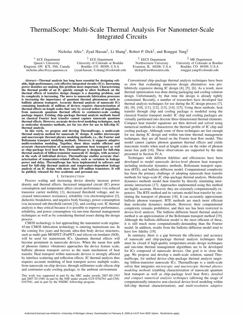
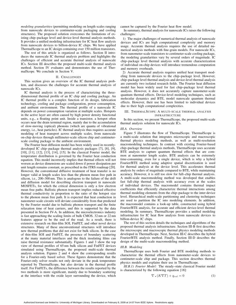
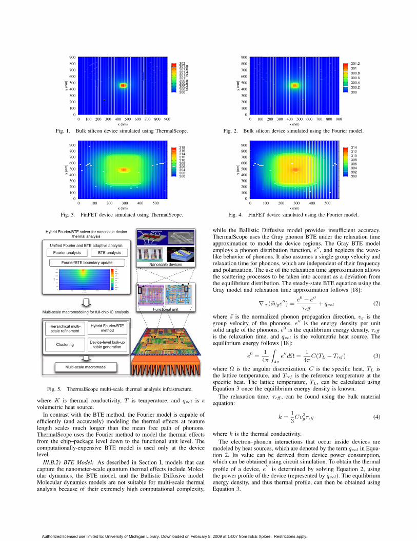
The Fourier heat diffusion model has been widely used in recently-developed IC chip–package thermal analysis packages [7], [8], [9],[10], [11], [12], [13], [14], [15]. In the classical Fourier model, thetemperature distribution is governed by the Fourier heat conductionequation. This model incorrectly implies that thermal effects will notworsen as device dimensions are scaled down if power dissipation perunit length remains constant, as prescribed in the ITRS roadmap [20].However, the conventional diffusive treatment of heat transfer is nolonger valid at length scales less than the phonon mean free path insilicon, i.e., 200–300 nm. This is analogous to the failure of the driftand diffusion model for describing electron transport in nanoscaleMOSFETs, for which the critical dimension is only a few electronmean free paths. Ballistic phonon transport implies reduced effectivethermal conductivity in proportion to the ratio of the hotspot sizeto the phonon mean free path. It is expected that heat conduction innanometer-scale circuits will deviate considerably from that predictedby the Fourier model due to ballistic phonon transport and the finiterelaxation time of heat carriers, and this is supported by the datapresented in Section IV-A. In addition, the microelectronics industryis fast approaching the scaling limits of bulk CMOS. 32 nm or 22 nmfeatures appear to be the end of the road. As a result, there isextensive research on thin-film SOI, FinFET, and other novel devicestructures. Many of these unconventional structures will introducenew thermal problems that did not exist for bulk silicon. In the caseof thin-film SOI and FinFET, the presence of boundary scatteringat the many material interfaces and the thick insulating films canraise thermal resistance substantially. Figures 1 and 3 show the topview of thermal profiles of 65 nm bulk silicon and FinFET devicessimulated using ThermalScope, the proposed multi-scale thermalanalysis solution. Figures 2 and 4 show the corresponding resultsfor a Fourier-only based solver. These figures demonstrate that theFourier-only solver results not only deviate in the peak temperaturereported by ThermalScope, but also deviate in the thermal profileitself. For FinFETs, the difference between the results reported by thetwo methods is more significant, mainly due to boundary scatteringat the interface with the oxide layer surrounding the device, which
cannot be captured by the Fourier heat flow model.In summary, thermal analysis for nanoscale ICs raises the following
challenges:
1) The major challenges of numerical thermal analysis of nanoscaledevices and ICs are high computational complexity and memoryusage. Accurate thermal analysis requires the use of detailed nu-merical analysis methods with fine-grain models. For nanoscale ICs,from nanometer-scale transistors to centimeter-scale cooling package,the modeling granularities vary by several orders of magnitude. ICchip–package level thermal analysis with accurate characterizationof individual on-chip devices will introduce tremendous computationand memory overheads.
2) Accurate thermal analysis requires unified heat transport mod-eling from nanoscale devices to the chip–package level. However,chip–package level thermal analysis and device-level thermal analysisare currently two isolated research fields. The Fourier heat diffusionmodel has been widely used for fast chip–package level thermalanalysis. However, it does not accurately capture nanometer-scalequantum thermal effects. Device-level modeling techniques, such asmolecular dynamics and BTE, model nanoscale quantum thermaleffects. However, their use has been limited to individual devicesdue to their high computational complexities.
III. THERMALSCOPE: A MULTI-SCALE THERMAL ANALYSIS
INFRASTRUCTURE
In this section, we present ThermalScope, the proposed multi-scalethermal analysis solution for nanoscale ICs.
III.A. Overview
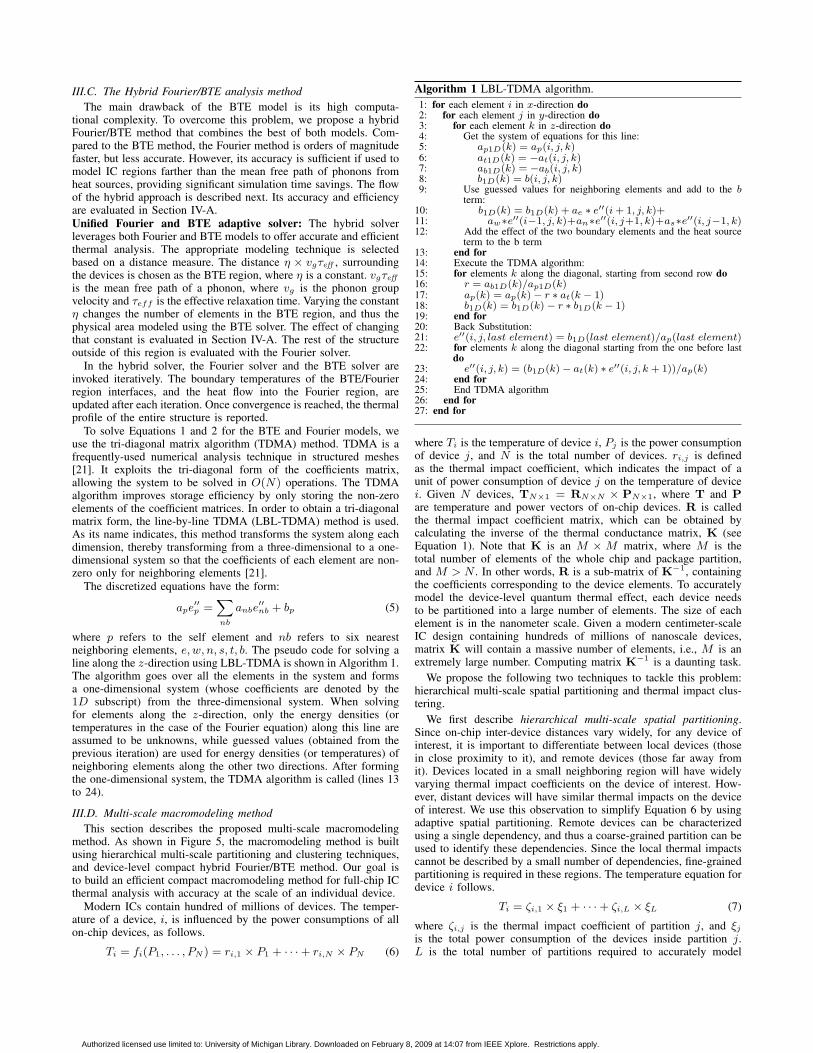
Figure 5 illustrates the flow of ThermalScope. ThermalScope isa multi-scale solution that integrates microscopic and macroscopicthermal physics modeling methods, as well as multi-resolutionmacromodeling techniques. In contrast with existing Fourier-basedchip–package thermal analysis methods, ThermalScope uses accurateBTE analysis to capture quantum thermal effects that are com-mon at nanometer length scales. BTE analysis can be extremelytime-consuming, even for a single device, which is why a hybridFourier/BTE method using adaptive spatial discretization is usedfor thermal analysis at the device level. This accelerates thermalanalysis by orders of magnitude compared to BTE, while maintainingaccuracy. However, it is still too slow for full–chip thermal analysis.A multi-scale macromodeling method was developed that enablesfast full-chip thermal analysis with accuracy even at the scalesof individual devices. The macromodel contains thermal impactcoefficients that efficiently characterize thermal interactions amongthermal modeling elements from the chip–package to the inter-devicelevel. Hierarchical multi-scale partitioning and clustering techniquesare used to partition the IC into modeling elements. In addition,the macromodel contains a look-up table, constructed using hybridFourier/BTE analysis, for accurate and efficient device-level thermalmodeling. In summary, ThermalScope provides a unified modelinginfrastructure for IC heat flow analysis from nanoscale devices tobillion-device IC chips.
The rest of this section details the techniques and algorithms of theproposed thermal analysis infrastructure. Section III-B first describesthe microscopic and macroscopic thermal physics modeling methodsdeveloped in ThermalScope. Next, Section III-C describes the hybridFourier/BTE analysis method. Finally, Section III-D describes thedesign of the multi-scale macromodeling method.
III.B. Modeling
ThermalScope uses both Fourier and BTE modeling methods tocharacterize the thermal effects from nanometer-scale devices tocentimeter-scale chip and package. This section describes thermalphysics models and explains their use in ThermalScope.
III.B.1) Fourier Model: The steady–state classical Fourier modelis characterized by the following equation [18]:
∇ (K∇T ) + qvol = 0 (1)
Authorized licensed use limited to: University of Michigan Library. Downloaded on February 8, 2009 at 14:07 from IEEE Xplore. Restrictions apply.
300 300.2 300.4 300.6 300.8 301 301.2 301.4 301.6 301.8 302
x (nm)
y (
nm
)
0 100 200 300 400 500 600 700 800 900
0
100
200
300
400
500
600
700
800
900
300
300.2
300.4
300.6
300.8
301
301.2
x (nm)
y (
nm
)
0 100 200 300 400 500 600 700 800 900
0
100
200
300
400
500
600
700
800
900
Fig. 1. Bulk silicon device simulated using ThermalScope. Fig. 2. Bulk silicon device simulated using the Fourier model.
300 302 304 306 308 310 312 314 316 318
x (nm)
y (
nm
)
0 100 200 300 400 500
0
100
200
300
400
500
600
700
800
900
300 302 304 306 308 310 312 314
x (nm)
y (
nm
)
0 100 200 300 400 500
0
100
200
300
400
500
600
700
800
900
Fig. 3. FinFET device simulated using ThermalScope. Fig. 4. FinFET device simulated using the Fourier model.
Functional unit
Nanoscale devices
Multi-scale macromodeling for full-chip IC analysis
Unified Fourier and BTE adaptive analysis
Fourier analysis BTE analysis
Fourier/BTE boundary update
Hybrid Fourier/BTE solver for nanoscale device thermal analysis
Hierarchical multi-scale refinement
ClusteringDevice-level look-up
table generation
Hybrid Fourier/BTE method
Multi-scale macromodel
300
300.5
301
301.5
302
302.5
303
303.5
304
304.5
0 500 1000 1500 2000
y (nm)
0
50
100
150
200
250
300
z (n
m)
Fig. 5. ThermalScope multi-scale thermal analysis infrastructure.
where K is thermal conductivity, T is temperature, and qvol is avolumetric heat source.
In contrast with the BTE method, the Fourier model is capable ofefficiently (and accurately) modeling the thermal effects at featurelength scales much longer than the mean free path of phonons.ThermalScope uses the Fourier method to model the thermal effectsfrom the chip–package level down to the functional unit level. Thecomputationally-expensive BTE model is used only at the devicelevel.
III.B.2) BTE Model: As described in Section I, models that cancapture the nanometer-scale quantum thermal effects include Molec-ular dynamics, the BTE model, and the Ballistic Diffusive model.Molecular dynamics models are not suitable for multi-scale thermalanalysis because of their extremely high computational complexity,
while the Ballistic Diffusive model provides insufficient accuracy.ThermalScope uses the Gray phonon BTE under the relaxation timeapproximation to model the device regions. The Gray BTE modelemploys a phonon distribution function, e′′, and neglects the wave-like behavior of phonons. It also assumes a single group velocity andrelaxation time for phonons, which are independent of their frequencyand polarization. The use of the relaxation time approximation allowsthe scattering processes to be taken into account as a deviation fromthe equilibrium distribution. The steady-state BTE equation using theGray model and relaxation time approximation follows [18]:
∇ (svge′′) =
e0− e′′
τeff
+ qvol (2)
where s is the normalized phonon propagation direction, vg is thegroup velocity of the phonons, e′′ is the energy density per unitsolid angle of the phonons, e0 is the equilibrium energy density, τeff
is the relaxation time, and qvol is the volumetric heat source. Theequilibrium energy follows [18]:
e0 =
1
4π
Z
4π
e′′dΩ =
1
4πC(TL − Tref ) (3)
where Ω is the angular discretization, C is the specific heat, TL isthe lattice temperature, and Tref is the reference temperature at thespecific heat. The lattice temperature, TL, can be calculated usingEquation 3 once the equilibrium energy density is known.
The relaxation time, τeff , can be found using the bulk materialequation:
k =1
3Cv
2
gτeff (4)
where k is the thermal conductivity.
The electron–phonon interactions that occur inside devices aremodeled by heat sources, which are denoted by the term qvol in Equa-tion 2. Its value can be derived from device power consumption,which can be obtained using circuit simulation. To obtain the thermal
profile of a device, e′′
is determined by solving Equation 2, usingthe power profile of the device (represented by qvol). The equilibriumenergy density, and thus thermal profile, can then be obtained usingEquation 3.
Authorized licensed use limited to: University of Michigan Library. Downloaded on February 8, 2009 at 14:07 from IEEE Xplore. Restrictions apply.
III.C. The Hybrid Fourier/BTE analysis method
The main drawback of the BTE model is its high computa-tional complexity. To overcome this problem, we propose a hybridFourier/BTE method that combines the best of both models. Com-pared to the BTE method, the Fourier method is orders of magnitudefaster, but less accurate. However, its accuracy is sufficient if used tomodel IC regions farther than the mean free path of phonons fromheat sources, providing significant simulation time savings. The flowof the hybrid approach is described next. Its accuracy and efficiencyare evaluated in Section IV-A.
Unified Fourier and BTE adaptive solver: The hybrid solverleverages both Fourier and BTE models to offer accurate and efficientthermal analysis. The appropriate modeling technique is selectedbased on a distance measure. The distance η × vgτeff , surroundingthe devices is chosen as the BTE region, where η is a constant. vgτeff
is the mean free path of a phonon, where vg is the phonon groupvelocity and τeff is the effective relaxation time. Varying the constantη changes the number of elements in the BTE region, and thus thephysical area modeled using the BTE solver. The effect of changingthat constant is evaluated in Section IV-A. The rest of the structureoutside of this region is evaluated with the Fourier solver.
In the hybrid solver, the Fourier solver and the BTE solver areinvoked iteratively. The boundary temperatures of the BTE/Fourierregion interfaces, and the heat flow into the Fourier region, areupdated after each iteration. Once convergence is reached, the thermalprofile of the entire structure is reported.
To solve Equations 1 and 2 for the BTE and Fourier models, weuse the tri-diagonal matrix algorithm (TDMA) method. TDMA is afrequently-used numerical analysis technique in structured meshes[21]. It exploits the tri-diagonal form of the coefficients matrix,allowing the system to be solved in O(N) operations. The TDMAalgorithm improves storage efficiency by only storing the non-zeroelements of the coefficient matrices. In order to obtain a tri-diagonalmatrix form, the line-by-line TDMA (LBL-TDMA) method is used.As its name indicates, this method transforms the system along eachdimension, thereby transforming from a three-dimensional to a one-dimensional system so that the coefficients of each element are non-zero only for neighboring elements [21].
The discretized equations have the form:
ape′′
p =X
nb
anbe′′
nb + bp (5)
where p refers to the self element and nb refers to six nearestneighboring elements, e, w, n, s, t, b. The pseudo code for solving aline along the z-direction using LBL-TDMA is shown in Algorithm 1.The algorithm goes over all the elements in the system and formsa one-dimensional system (whose coefficients are denoted by the1D subscript) from the three-dimensional system. When solvingfor elements along the z-direction, only the energy densities (ortemperatures in the case of the Fourier equation) along this line areassumed to be unknowns, while guessed values (obtained from theprevious iteration) are used for energy densities (or temperatures) ofneighboring elements along the other two directions. After formingthe one-dimensional system, the TDMA algorithm is called (lines 13to 24).
III.D. Multi-scale macromodeling method
This section describes the proposed multi-scale macromodelingmethod. As shown in Figure 5, the macromodeling method is builtusing hierarchical multi-scale partitioning and clustering techniques,and device-level compact hybrid Fourier/BTE method. Our goal isto build an efficient compact macromodeling method for full-chip ICthermal analysis with accuracy at the scale of an individual device.
Modern ICs contain hundred of millions of devices. The temper-ature of a device, i, is influenced by the power consumptions of allon-chip devices, as follows.
Ti = fi(P1, . . . , PN ) = ri,1 × P1 + · · · + ri,N × PN (6)
Algorithm 1 LBL-TDMA algorithm.
1: for each element i in x-direction do2: for each element j in y-direction do3: for each element k in z-direction do4: Get the system of equations for this line:5: ap1D(k) = ap(i, j, k)6: at1D(k) = −at(i, j, k)7: ab1D(k) = −ab(i, j, k)8: b1D(k) = b(i, j, k)9: Use guessed values for neighboring elements and add to the b
term:10: b1D(k) = b1D(k) + ae ∗ e′′(i + 1, j, k)+11: aw∗e′′(i−1, j, k)+an∗e′′(i, j+1, k)+as∗e′′(i, j−1, k)12: Add the effect of the two boundary elements and the heat source
term to the b term13: end for14: Execute the TDMA algorithm:15: for elements k along the diagonal, starting from second row do16: r = ab1D(k)/ap1D(k)17: ap(k) = ap(k) − r ∗ at(k − 1)18: b1D(k) = b1D(k) − r ∗ b1D(k − 1)19: end for20: Back Substitution:21: e′′(i, j, last element) = b1D(last element)/ap(last element)22: for elements k along the diagonal starting from the one before last
do23: e′′(i, j, k) = (b1D(k) − at(k) ∗ e′′(i, j, k + 1))/ap(k)24: end for25: End TDMA algorithm26: end for27: end for
where Ti is the temperature of device i, Pj is the power consumptionof device j, and N is the total number of devices. ri,j is definedas the thermal impact coefficient, which indicates the impact of aunit of power consumption of device j on the temperature of devicei. Given N devices, TN×1 = RN×N × PN×1, where T and P
are temperature and power vectors of on-chip devices. R is calledthe thermal impact coefficient matrix, which can be obtained bycalculating the inverse of the thermal conductance matrix, K (seeEquation 1). Note that K is an M × M matrix, where M is thetotal number of elements of the whole chip and package partition,and M > N . In other words, R is a sub-matrix of K
−1, containingthe coefficients corresponding to the device elements. To accuratelymodel the device-level quantum thermal effect, each device needsto be partitioned into a large number of elements. The size of eachelement is in the nanometer scale. Given a modern centimeter-scaleIC design containing hundreds of millions of nanoscale devices,matrix K will contain a massive number of elements, i.e., M is anextremely large number. Computing matrix K
−1 is a daunting task.
We propose the following two techniques to tackle this problem:hierarchical multi-scale spatial partitioning and thermal impact clus-tering.
We first describe hierarchical multi-scale spatial partitioning.Since on-chip inter-device distances vary widely, for any device ofinterest, it is important to differentiate between local devices (thosein close proximity to it), and remote devices (those far away fromit). Devices located in a small neighboring region will have widelyvarying thermal impact coefficients on the device of interest. How-ever, distant devices will have similar thermal impacts on the deviceof interest. We use this observation to simplify Equation 6 by usingadaptive spatial partitioning. Remote devices can be characterizedusing a single dependency, and thus a coarse-grained partition can beused to identify these dependencies. Since the local thermal impactscannot be described by a small number of dependencies, fine-grainedpartitioning is required in these regions. The temperature equation fordevice i follows.
Ti = ζi,1 × ξ1 + · · · + ζi,L × ξL (7)
where ζi,j is the thermal impact coefficient of partition j, and ξj
is the total power consumption of the devices inside partition j.L is the total number of partitions required to accurately model
Authorized licensed use limited to: University of Michigan Library. Downloaded on February 8, 2009 at 14:07 from IEEE Xplore. Restrictions apply.
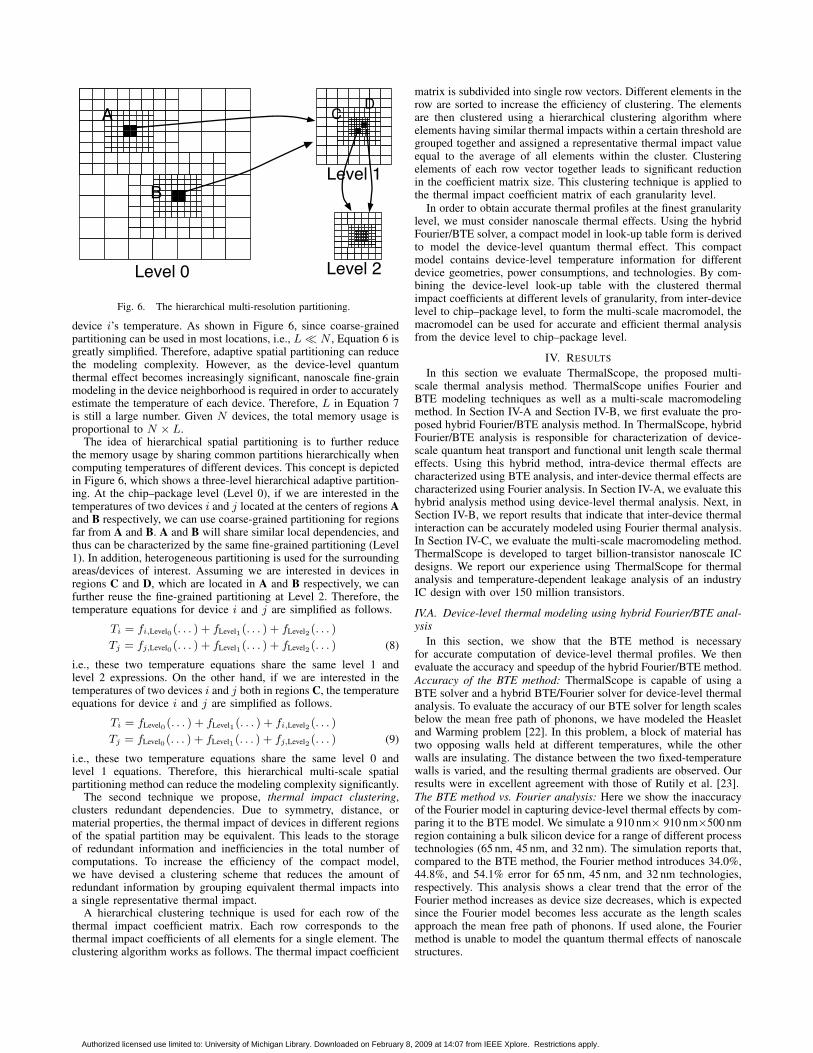
CD
A
B
Level 0
Level 1
Level 2
Fig. 6. The hierarchical multi-resolution partitioning.
device i’s temperature. As shown in Figure 6, since coarse-grainedpartitioning can be used in most locations, i.e., L ≪ N , Equation 6 isgreatly simplified. Therefore, adaptive spatial partitioning can reducethe modeling complexity. However, as the device-level quantumthermal effect becomes increasingly significant, nanoscale fine-grainmodeling in the device neighborhood is required in order to accuratelyestimate the temperature of each device. Therefore, L in Equation 7is still a large number. Given N devices, the total memory usage isproportional to N × L.
The idea of hierarchical spatial partitioning is to further reducethe memory usage by sharing common partitions hierarchically whencomputing temperatures of different devices. This concept is depictedin Figure 6, which shows a three-level hierarchical adaptive partition-ing. At the chip–package level (Level 0), if we are interested in thetemperatures of two devices i and j located at the centers of regions Aand B respectively, we can use coarse-grained partitioning for regionsfar from A and B. A and B will share similar local dependencies, andthus can be characterized by the same fine-grained partitioning (Level1). In addition, heterogeneous partitioning is used for the surroundingareas/devices of interest. Assuming we are interested in devices inregions C and D, which are located in A and B respectively, we canfurther reuse the fine-grained partitioning at Level 2. Therefore, thetemperature equations for device i and j are simplified as follows.
Ti = fi,Level0(. . . ) + fLevel1(. . . ) + fLevel2(. . . )
Tj = fj,Level0(. . . ) + fLevel1(. . . ) + fLevel2(. . . ) (8)
i.e., these two temperature equations share the same level 1 andlevel 2 expressions. On the other hand, if we are interested in thetemperatures of two devices i and j both in regions C, the temperatureequations for device i and j are simplified as follows.
Ti = fLevel0(. . . ) + fLevel1(. . . ) + fi,Level2(. . . )
Tj = fLevel0(. . . ) + fLevel1(. . . ) + fj,Level2(. . . ) (9)
i.e., these two temperature equations share the same level 0 andlevel 1 equations. Therefore, this hierarchical multi-scale spatialpartitioning method can reduce the modeling complexity significantly.
The second technique we propose, thermal impact clustering,clusters redundant dependencies. Due to symmetry, distance, ormaterial properties, the thermal impact of devices in different regionsof the spatial partition may be equivalent. This leads to the storageof redundant information and inefficiencies in the total number ofcomputations. To increase the efficiency of the compact model,we have devised a clustering scheme that reduces the amount ofredundant information by grouping equivalent thermal impacts intoa single representative thermal impact.
A hierarchical clustering technique is used for each row of thethermal impact coefficient matrix. Each row corresponds to thethermal impact coefficients of all elements for a single element. Theclustering algorithm works as follows. The thermal impact coefficient
matrix is subdivided into single row vectors. Different elements in therow are sorted to increase the efficiency of clustering. The elementsare then clustered using a hierarchical clustering algorithm whereelements having similar thermal impacts within a certain threshold aregrouped together and assigned a representative thermal impact valueequal to the average of all elements within the cluster. Clusteringelements of each row vector together leads to significant reductionin the coefficient matrix size. This clustering technique is applied tothe thermal impact coefficient matrix of each granularity level.
In order to obtain accurate thermal profiles at the finest granularitylevel, we must consider nanoscale thermal effects. Using the hybridFourier/BTE solver, a compact model in look-up table form is derivedto model the device-level quantum thermal effect. This compactmodel contains device-level temperature information for differentdevice geometries, power consumptions, and technologies. By com-bining the device-level look-up table with the clustered thermalimpact coefficients at different levels of granularity, from inter-devicelevel to chip–package level, to form the multi-scale macromodel, themacromodel can be used for accurate and efficient thermal analysisfrom the device level to chip–package level.
IV. RESULTS
In this section we evaluate ThermalScope, the proposed multi-scale thermal analysis method. ThermalScope unifies Fourier andBTE modeling techniques as well as a multi-scale macromodelingmethod. In Section IV-A and Section IV-B, we first evaluate the pro-posed hybrid Fourier/BTE analysis method. In ThermalScope, hybridFourier/BTE analysis is responsible for characterization of device-scale quantum heat transport and functional unit length scale thermaleffects. Using this hybrid method, intra-device thermal effects arecharacterized using BTE analysis, and inter-device thermal effects arecharacterized using Fourier analysis. In Section IV-A, we evaluate thishybrid analysis method using device-level thermal analysis. Next, inSection IV-B, we report results that indicate that inter-device thermalinteraction can be accurately modeled using Fourier thermal analysis.In Section IV-C, we evaluate the multi-scale macromodeling method.ThermalScope is developed to target billion-transistor nanoscale ICdesigns. We report our experience using ThermalScope for thermalanalysis and temperature-dependent leakage analysis of an industryIC design with over 150 million transistors.
IV.A. Device-level thermal modeling using hybrid Fourier/BTE anal-ysis
In this section, we show that the BTE method is necessaryfor accurate computation of device-level thermal profiles. We thenevaluate the accuracy and speedup of the hybrid Fourier/BTE method.
Accuracy of the BTE method: ThermalScope is capable of using aBTE solver and a hybrid BTE/Fourier solver for device-level thermalanalysis. To evaluate the accuracy of our BTE solver for length scalesbelow the mean free path of phonons, we have modeled the Heasletand Warming problem [22]. In this problem, a block of material hastwo opposing walls held at different temperatures, while the otherwalls are insulating. The distance between the two fixed-temperaturewalls is varied, and the resulting thermal gradients are observed. Ourresults were in excellent agreement with those of Rutily et al. [23].
The BTE method vs. Fourier analysis: Here we show the inaccuracyof the Fourier model in capturing device-level thermal effects by com-paring it to the BTE model. We simulate a 910 nm× 910 nm×500 nmregion containing a bulk silicon device for a range of different processtechnologies (65 nm, 45 nm, and 32 nm). The simulation reports that,compared to the BTE method, the Fourier method introduces 34.0%,44.8%, and 54.1% error for 65 nm, 45 nm, and 32 nm technologies,respectively. This analysis shows a clear trend that the error of theFourier method increases as device size decreases, which is expectedsince the Fourier model becomes less accurate as the length scalesapproach the mean free path of phonons. If used alone, the Fouriermethod is unable to model the quantum thermal effects of nanoscalestructures.
Authorized licensed use limited to: University of Michigan Library. Downloaded on February 8, 2009 at 14:07 from IEEE Xplore. Restrictions apply.
0
2
4
6
8
10
12
14
16
18
0 1 2 3 4 5
1
10
100
1000E
rro
r (%
)
Sp
ee
du
p
The number of mean free paths the BTE region is extended
Error for 65nmSpeedup for 65nm
Error for 45nmSpeedup for 45nm
Error for 32nmSpeedup for 32nm
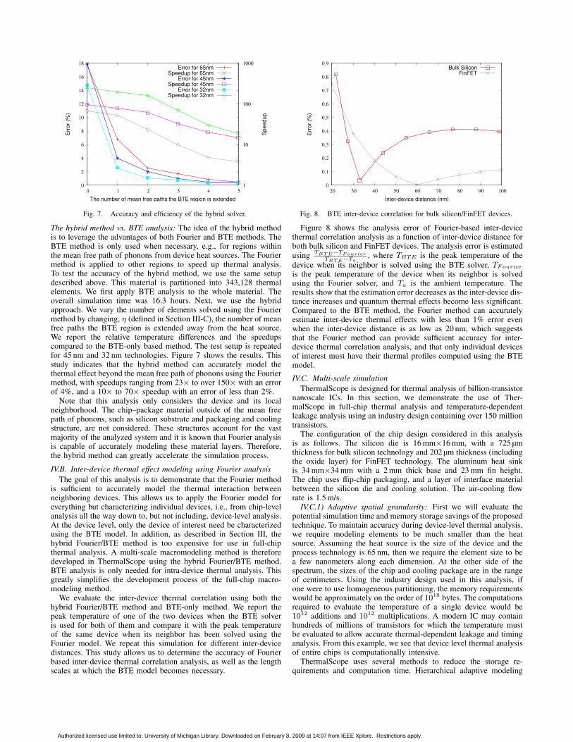
Fig. 7. Accuracy and efficiency of the hybrid solver.
The hybrid method vs. BTE analysis: The idea of the hybrid methodis to leverage the advantages of both Fourier and BTE methods. TheBTE method is only used when necessary, e.g., for regions withinthe mean free path of phonons from device heat sources. The Fouriermethod is applied to other regions to speed up thermal analysis.To test the accuracy of the hybrid method, we use the same setupdescribed above. This material is partitioned into 343,128 thermalelements. We first apply BTE analysis to the whole material. Theoverall simulation time was 16.3 hours. Next, we use the hybridapproach. We vary the number of elements solved using the Fouriermethod by changing, η (defined in Section III-C), the number of meanfree paths the BTE region is extended away from the heat source.We report the relative temperature differences and the speedupscompared to the BTE-only based method. The test setup is repeatedfor 45 nm and 32 nm technologies. Figure 7 shows the results. Thisstudy indicates that the hybrid method can accurately model thethermal effect beyond the mean free path of phonons using the Fouriermethod, with speedups ranging from 23× to over 150× with an errorof 4%, and a 10× to 70× speedup with an error of less than 2%.
Note that this analysis only considers the device and its localneighborhood. The chip–package material outside of the mean freepath of phonons, such as silicon substrate and packaging and coolingstructure, are not considered. These structures account for the vastmajority of the analyzed system and it is known that Fourier analysisis capable of accurately modeling these material layers. Therefore,the hybrid method can greatly accelerate the simulation process.
IV.B. Inter-device thermal effect modeling using Fourier analysis
The goal of this analysis is to demonstrate that the Fourier methodis sufficient to accurately model the thermal interaction betweenneighboring devices. This allows us to apply the Fourier model foreverything but characterizing individual devices, i.e., from chip-levelanalysis all the way down to, but not including, device-level analysis.At the device level, only the device of interest need be characterizedusing the BTE model. In addition, as described in Section III, thehybrid Fourier/BTE method is too expensive for use in full-chipthermal analysis. A multi-scale macromodeling method is thereforedeveloped in ThermalScope using the hybrid Fourier/BTE method.BTE analysis is only needed for intra-device thermal analysis. Thisgreatly simplifies the development process of the full-chip macro-modeling method.
We evaluate the inter-device thermal correlation using both thehybrid Fourier/BTE method and BTE-only method. We report thepeak temperature of one of the two devices when the BTE solveris used for both of them and compare it with the peak temperatureof the same device when its neighbor has been solved using theFourier model. We repeat this simulation for different inter-devicedistances. This study allows us to determine the accuracy of Fourierbased inter-device thermal correlation analysis, as well as the lengthscales at which the BTE model becomes necessary.
0
0.1
0.2
0.3
0.4
0.5
0.6
0.7
0.8
0.9
20 30 40 50 60 70 80 90 100
Err
or
(%)
Inter-device distance (nm)
Bulk SiliconFinFET
Fig. 8. BTE inter-device correlation for bulk silicon/FinFET devices.
Figure 8 shows the analysis error of Fourier-based inter-devicethermal correlation analysis as a function of inter-device distance forboth bulk silicon and FinFET devices. The analysis error is estimated
usingTBT E−TF ourier
TBT E−Ta, where TBTE is the peak temperature of the
device when its neighbor is solved using the BTE solver, TFourier
is the peak temperature of the device when its neighbor is solvedusing the Fourier solver, and Ta is the ambient temperature. Theresults show that the estimation error decreases as the inter-device dis-tance increases and quantum thermal effects become less significant.Compared to the BTE method, the Fourier method can accuratelyestimate inter-device thermal effects with less than 1% error evenwhen the inter-device distance is as low as 20 nm, which suggeststhat the Fourier method can provide sufficient accuracy for inter-device thermal correlation analysis, and that only individual devicesof interest must have their thermal profiles computed using the BTEmodel.
IV.C. Multi-scale simulation
ThermalScope is designed for thermal analysis of billion-transistornanoscale ICs. In this section, we demonstrate the use of Ther-malScope in full-chip thermal analysis and temperature-dependentleakage analysis using an industry design containing over 150 milliontransistors.
The configuration of the chip design considered in this analysisis as follows. The silicon die is 16 mm×16 mm, with a 725 µmthickness for bulk silicon technology and 202 µm thickness (includingthe oxide layer) for FinFET technology. The aluminum heat sinkis 34 mm×34 mm with a 2 mm thick base and 23 mm fin height.The chip uses flip-chip packaging, and a layer of interface materialbetween the silicon die and cooling solution. The air-cooling flowrate is 1.5 m/s.
IV.C.1) Adaptive spatial granularity: First we will evaluate thepotential simulation time and memory storage savings of the proposedtechnique. To maintain accuracy during device-level thermal analysis,we require modeling elements to be much smaller than the heatsource. Assuming the heat source is the size of the device and theprocess technology is 65 nm, then we require the element size to bea few nanometers along each dimension. At the other side of thespectrum, the sizes of the chip and cooling package are in the rangeof centimeters. Using the industry design used in this analysis, ifone were to use homogeneous partitioning, the memory requirementswould be approximately on the order of 1018 bytes. The computationsrequired to evaluate the temperature of a single device would be1012 additions and 1012 multiplications. A modern IC may containhundreds of millions of transistors for which the temperature mustbe evaluated to allow accurate thermal-dependent leakage and timinganalysis. From this example, we see that device level thermal analysisof entire chips is computationally intensive.
ThermalScope uses several methods to reduce the storage re-quirements and computation time. Hierarchical adaptive modeling
Authorized licensed use limited to: University of Michigan Library. Downloaded on February 8, 2009 at 14:07 from IEEE Xplore. Restrictions apply.
granularities are used from the chip level down to the inter-devicelevel. This adaptive modeling reduces the problem size to requiringstorage on the order of 108 bytes for the thermal impact coefficientmatrices for the same problem as described above. For comparison,the input power profile of the industry design itself requires morethan 7×108 bytes of storage. The computations required to evaluatethe temperature of a single device would also be reduced to 108
additions and multiplications, and the results from the majority ofthese computations can be reused among devices. The amount ofcomputation is further reduced by clustering. The simulation run-timeand memory usage results for the device-level temperature evaluation(after obtaining the coefficient matrices) for clustering are shown inTable I. The chip evaluated contained over 150 million devices andwas evaluated for both a bulk silicon design and a FinFET design. Theresults show that although the memory usage may not be significantlyreduced using a clustering technique, significant speed-up can beachieved. For the clustering technique, memory usage for indexing isrequired in addition to storing the clustered information, which canexplain the lack of significant memory reduction.
TABLE IEFFICIENCY EVALUATION.
Bulk silicon FinFET
Clustering No clustering Clustering No clustering
tCP U (min) 167 485 179 607
Memory (MB) 548 604 620 604
IV.C.2) Thermal Analysis and Temperature-Dependent LeakagePower Estimation: Accurate thermal analysis is critical for evalu-ation of temperature-dependent effects. ThermalScope is capable ofhandling large IC designs with device-level accuracy. In this section,we report the use of ThermalScope for full-chip thermal analysis andtemperature-dependent IC leakage analysis using the large industrydesign.
Since the leakage power of the chip is strongly affected by temper-ature, it is necessary to include the leakage power estimation in thethermal analysis simulation flow. To determine thermal profile whiletaking into account the leakage power, the following iterative processcan be used. From the data set of the industry design, the initialdynamic and leakage power are estimated at the ambient temperatureof 55C. The device-level thermal profile is then evaluated for thegiven initial power. The results of this simulation are then used toupdate the leakage power of the chip. This iterative process continuesuntil convergence is reached for the simulated thermal and the powerprofiles. In this study, the temperature-leakage power dependency isobtained using curve fitting of a measured industrial design data set,which contains power numbers for various temperatures.
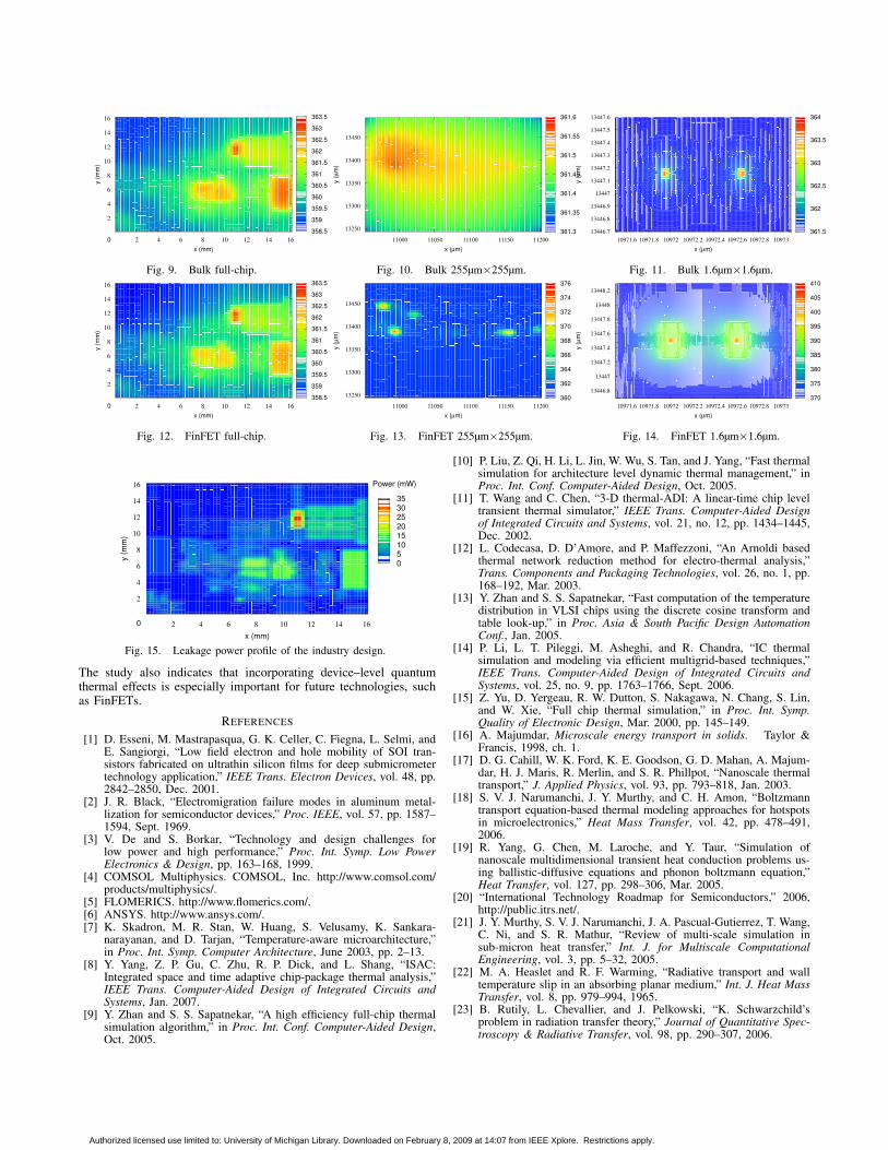
We consider both bulk silicon and FinFET technologies. Thethermal profile of the IC design is characterized using the multi-scalemacromodeling method using the described iterative analysis process.During thermal analysis, the temperature of every device is evaluated,and the leakage power of each device is adjusted based on its changein temperature. This process is carried out for every single deviceon the chip. The temperature profiles obtained for three differentlevels of granularity are shown in Figures 9 through 11 for bulksilicon technology, and Figures 12 through 14 for FinFET technology.Figures 10 and 13 are enlarged fine-grained thermal profiles of ahotspot on the chip. Figures 11 and 14 illustrate a further enlargementof the area, showing the device-level information for two devicesout of the hundreds of millions for which temperature is calculated.Although ThermalScope evaluates the temperature of every device,it is also capable of coarse-grained thermal analysis. The thermalprofiles demonstrate the capability of ThermalScope to evaluate thethermal profile at different scales, which vary through six orders ofmagnitude. The profiles also indicate the inaccuracy resulting fromusing coarse-grained estimates of device temperatures.
Figures 9 through 14 show the information lost when device-
level thermal analysis is not considered. Using coarse-grained ther-mal analysis, large inaccuracies occur due to the assumption thatall devices within a single coarse-grained element have the sametemperature. For the bulk silicon designs, at the intermediate level(255µm×255µm) this may be a valid assumption, however at thedevice level we clearly see a significant deviation from the averagecoarse-grained temperature. This demonstrates that thermal analysisof the entire chip at the intermediate level would not be sufficient tocharacterize device temperatures. The strength of ThermalScope isthat it reports the temperature of each device allowing detailed full-chip thermal analysis. In coarse-grained thermal analysis, the featuresoccurring at device level are not considered, which leads to inaccurateestimation of device temperatures, as shown in Figures 9–14.
In addition to thermal analysis, ThermalScope can also be usedto estimate the leakage power. The leakage power is determined bythe same iterative process described earlier. We have compared theresults of the leakage power obtained using four distinct techniques.
The first leakage power value to be compared, P1, is the leakagepower from the industrial benchmark data set at an ambient tempera-ture of 55C. The second leakage power, P2, was obtained by estimat-ing the leakage power after full-chip thermal analysis, using device-level modeling granularity. The third and fourth leakage powers wereevaluated using the iterative process. The iterative process was carriedout for both the coarse-grained thermal analysis (chip divided into64×64 elements) for P3, and full-chip thermal analysis, using device-level modeling granularity for P4. By comparing the leakage powerobtained with the various techniques, we can gain insight into theimportance of device-level information on leakage power estimationand the significance of iterative solutions. The leakage power resultsare presented in Table II.
The results indicate that iterative solutions converge to a signif-icantly higher leakage power and thus single-iteration evaluationmethods are not sufficient for accurate leakage power estimation.The results also demonstrates the effect of considering device-levelthermal behavior during leakage analysis. For both the FinFET andbulk silicon designs, the leakage power reported using multipleiterations of device-level thermal analysis is higher than the otherleakage powers reported. The leakage power profile of the industrydesign, obtained using the iterative full-chip thermal analysis withdevice-level modeling granularity technique is shown in Figure 15.
From the results presented in this section, we can conclude thatdevice-level thermal analysis is necessary for both accurate thermalprofile information, and leakage power estimation. By using a com-pact macromodeling method, ThermalScope is able to obtain thisinformation given reasonable time and storage.
TABLE IILEAKAGE POWER ESTIMATION.
P1 P2 P3 P4
Bulk silicon Pleak (mW) 13277.4 16452.5 16454.3 16563.4
FinFET Pleak (mW) 13277.4 16565.0 16242.6 16983.8
V. CONCLUSIONS
Thermal analysis and optimization are now critical in nanoscaleIC design. The goal of this work is to develop thermal modelingtechniques that are accurate at nanometer length scales and alsocomputationally-efficient for full-chip thermal analysis. To achievethis goal, we have developed ThermalScope, a multi-scale thermalanalysis solution. It unifies microscopic and macroscopic thermalphysics modeling methods and multi-resolution adaptive macromod-eling methods, permitting accurate thermal modeling on length scalesranging from nanoscale devices to centimeter-scale packaging andcooling structures. We have used ThermalScope in a large IC designconsisting of more than 150 million transistors. The study shows thatThermalScope is suitable for thermal analysis and characterizationof thermal-related effects for billion-transistor nanoscale IC designs.
Authorized licensed use limited to: University of Michigan Library. Downloaded on February 8, 2009 at 14:07 from IEEE Xplore. Restrictions apply.
358.5
359
359.5
360
360.5
361
361.5
362
362.5
363
363.5
x (mm)
y (
mm
)
0 2 4 6 8 10 12 14 16
2
4
6
8
10
12
14
16
361.3
361.35
361.4
361.45
361.5
361.55
361.6
11000 11050 11100 11150 11200
x (µm)
13250
13300
13350
13400
13450
y (
µm
)
361.5
362
362.5
363
363.5
364
10971.6 10971.8 10972 10972.2 10972.4 10972.6 10972.8 10973
x (µm)
13446.7
13446.8
13446.9
13447
13447.1
13447.2
13447.3
13447.4
13447.5
13447.6
y (
µm
)
Fig. 9. Bulk full-chip. Fig. 10. Bulk 255µm×255µm. Fig. 11. Bulk 1.6µm×1.6µm.
358.5
359
359.5
360
360.5
361
361.5
362
362.5
363
363.5
x (mm)
y (
mm
)
0 2 4 6 8 10 12 14 16
2
4
6
8
10
12
14
16
360
362
364
366
368
370
372
374
376
11000 11050 11100 11150 11200
x (µm)
13250
13300
13350
13400
13450
y (
µm
)
370
375
380
385
390
395
400
405
410
10971.6 10971.8 10972 10972.2 10972.4 10972.6 10972.8 10973
x (µm)
13446.8
13447
13447.2
13447.4
13447.6
13447.8
13448
13448.2
y (
µm
)
Fig. 12. FinFET full-chip. Fig. 13. FinFET 255µm×255µm. Fig. 14. FinFET 1.6µm×1.6µm.
0 5 10 15 20 25 30 35
x (mm)
y (
mm
)
Power (mW)
0 2 4 6 8 10 12 14 16
2
4
6
8
10
12
14
16
Fig. 15. Leakage power profile of the industry design.
The study also indicates that incorporating device–level quantumthermal effects is especially important for future technologies, suchas FinFETs.
REFERENCES
[1] D. Esseni, M. Mastrapasqua, G. K. Celler, C. Fiegna, L. Selmi, andE. Sangiorgi, “Low field electron and hole mobility of SOI tran-sistors fabricated on ultrathin silicon films for deep submicrometertechnology application,” IEEE Trans. Electron Devices, vol. 48, pp.2842–2850, Dec. 2001.
[2] J. R. Black, “Electromigration failure modes in aluminum metal-lization for semiconductor devices,” Proc. IEEE, vol. 57, pp. 1587–1594, Sept. 1969.
[3] V. De and S. Borkar, “Technology and design challenges forlow power and high performance,” Proc. Int. Symp. Low PowerElectronics & Design, pp. 163–168, 1999.
[4] COMSOL Multiphysics. COMSOL, Inc. http://www.comsol.com/products/multiphysics/.
[5] FLOMERICS. http://www.flomerics.com/.[6] ANSYS. http://www.ansys.com/.[7] K. Skadron, M. R. Stan, W. Huang, S. Velusamy, K. Sankara-
narayanan, and D. Tarjan, “Temperature-aware microarchitecture,”in Proc. Int. Symp. Computer Architecture, June 2003, pp. 2–13.
[8] Y. Yang, Z. P. Gu, C. Zhu, R. P. Dick, and L. Shang, “ISAC:Integrated space and time adaptive chip-package thermal analysis,”IEEE Trans. Computer-Aided Design of Integrated Circuits andSystems, Jan. 2007.
[9] Y. Zhan and S. S. Sapatnekar, “A high efficiency full-chip thermalsimulation algorithm,” in Proc. Int. Conf. Computer-Aided Design,Oct. 2005.
[10] P. Liu, Z. Qi, H. Li, L. Jin, W. Wu, S. Tan, and J. Yang, “Fast thermalsimulation for architecture level dynamic thermal management,” inProc. Int. Conf. Computer-Aided Design, Oct. 2005.
[11] T. Wang and C. Chen, “3-D thermal-ADI: A linear-time chip leveltransient thermal simulator,” IEEE Trans. Computer-Aided Designof Integrated Circuits and Systems, vol. 21, no. 12, pp. 1434–1445,Dec. 2002.
[12] L. Codecasa, D. D’Amore, and P. Maffezzoni, “An Arnoldi basedthermal network reduction method for electro-thermal analysis,”Trans. Components and Packaging Technologies, vol. 26, no. 1, pp.168–192, Mar. 2003.
[13] Y. Zhan and S. S. Sapatnekar, “Fast computation of the temperaturedistribution in VLSI chips using the discrete cosine transform andtable look-up,” in Proc. Asia & South Pacific Design AutomationConf., Jan. 2005.
[14] P. Li, L. T. Pileggi, M. Asheghi, and R. Chandra, “IC thermalsimulation and modeling via efficient multigrid-based techniques,”IEEE Trans. Computer-Aided Design of Integrated Circuits andSystems, vol. 25, no. 9, pp. 1763–1766, Sept. 2006.
[15] Z. Yu, D. Yergeau, R. W. Dutton, S. Nakagawa, N. Chang, S. Lin,and W. Xie, “Full chip thermal simulation,” in Proc. Int. Symp.Quality of Electronic Design, Mar. 2000, pp. 145–149.
[16] A. Majumdar, Microscale energy transport in solids. Taylor &Francis, 1998, ch. 1.
[17] D. G. Cahill, W. K. Ford, K. E. Goodson, G. D. Mahan, A. Majum-dar, H. J. Maris, R. Merlin, and S. R. Phillpot, “Nanoscale thermaltransport,” J. Applied Physics, vol. 93, pp. 793–818, Jan. 2003.
[18] S. V. J. Narumanchi, J. Y. Murthy, and C. H. Amon, “Boltzmanntransport equation-based thermal modeling approaches for hotspotsin microelectronics,” Heat Mass Transfer, vol. 42, pp. 478–491,2006.
[19] R. Yang, G. Chen, M. Laroche, and Y. Taur, “Simulation ofnanoscale multidimensional transient heat conduction problems us-ing ballistic-diffusive equations and phonon boltzmann equation,”Heat Transfer, vol. 127, pp. 298–306, Mar. 2005.
[20] “International Technology Roadmap for Semiconductors,” 2006,http://public.itrs.net/.
[21] J. Y. Murthy, S. V. J. Narumanchi, J. A. Pascual-Gutierrez, T. Wang,C. Ni, and S. R. Mathur, “Review of multi-scale simulation insub-micron heat transfer,” Int. J. for Multiscale ComputationalEngineering, vol. 3, pp. 5–32, 2005.
[22] M. A. Heaslet and R. F. Warming, “Radiative transport and walltemperature slip in an absorbing planar medium,” Int. J. Heat MassTransfer, vol. 8, pp. 979–994, 1965.
[23] B. Rutily, L. Chevallier, and J. Pelkowski, “K. Schwarzchild’sproblem in radiation transfer theory,” Journal of Quantitative Spec-troscopy & Radiative Transfer, vol. 98, pp. 290–307, 2006.
Authorized licensed use limited to: University of Michigan Library. Downloaded on February 8, 2009 at 14:07 from IEEE Xplore. Restrictions apply.