THERMAL PROPERTIES OF DISORDERED ORGANIC SOLIDS AND ...
151
THERMAL PROPERTIES OF DISORDERED ORGANIC SOLIDS AND INTERFACES INVOLVING ORGANICS by Yansha Jin A dissertation submitted in partial fulfillment of the requirements for the degree of Doctor of Philosophy (Materials Science and Engineering) in The University of Michigan 2013 Doctoral Committee: Associate Professor Max Shtein, Co-Chair Associate Professor Kevin P. Pipe, Co-Chair Professor Jay L. Guo Associate Professor Anton Van der Ven
Transcript of THERMAL PROPERTIES OF DISORDERED ORGANIC SOLIDS AND ...

THERMAL PROPERTIES OF DISORDEREDORGANIC SOLIDS AND INTERFACES
INVOLVING ORGANICS
by
Yansha Jin
A dissertation submitted in partial fulfillmentof the requirements for the degree of
Doctor of Philosophy(Materials Science and Engineering)
in The University of Michigan2013
Doctoral Committee:
Associate Professor Max Shtein, Co-ChairAssociate Professor Kevin P. Pipe, Co-ChairProfessor Jay L. GuoAssociate Professor Anton Van der Ven

c© Yansha Jin 2013
All Rights Reserved

ACKNOWLEDGEMENTS
First and foremost, I would like to express my profound gratitude to my committee
members: to the Chairs, Professor Max Shtein and Professor Kevin P. Pipe for their
support through my doctoral study and their wise guidance in research and invaluable
suggestions in life; to Professor Anton van der Ven and Professor L. Jay Guo, who has
for many years helped and encouraged me, their advice has helped substantially to my
study. Especially, I am deeply grateful to Professor Max Shtein. He has been a role
model in creativity thinking, work ethics and family values, and his encouragements
and suggestions during some frustrating periods in these five years were eminently
helpful to me. I am also very thankful to Professor Pramod Reddy and Professor
John Kieffer for their valuable input to my research.
I am pleased to acknowledge the financial support from United States Air Force
Office of Scientific Research under Grant No. FA9550-080-1-0340 throughout the Mul-
tidisciplinary University Research Initiative Program. The gratitude also extended to
Rackham graduate school - Barbour scholarship program and University of Michigan,
Materials Sciences and Engineering department.
I owe a great deal to many fellow students in my research lab and other labs I have
worked and collaborated at various stages of my doctoral study: Kanika Agrawal,
Kwang Hyup An, Adam Barito, Andrea Bianchini, Shaurjo Biswas, Victor Chan,
Susan Gentry, Chelsea Haughn, Mark Hendryx, Lei Jiang, Jongdoo Ju, Myungkoo
Kang, Gunho Kim, Jingjing Li, Steven Morris, Denis Northern, Olga Shalev, Chen
Shao, Huarui Sun, Matt Sykes, Abhishek Yadav, Kejia Zhang, Yiying Zhao and many
ii

others. I would like to offer my sincere thanks to Abhishek Yadav for unselfishly
teaching and helping me in the starting stage of my project with endless patience,
also for buying me my first beer in Ann Arbor; To Yiying Zhao for being my best
friend in the lab and I am constantly amazed by her personality and her wisdom
in life; To my lovely peers Steven Morris and Shaurjo Biswas who has always been
there for me, it has been a real pleasure to have my the most pessimistic and most
optimistic friends’ accompany.
My heartfelt appreciation also goes out to all my friends. Especially, to my dearest
Emmy Lei who has been my best friend for 8 years, from the Beijing days to the Ann
Arbor era; To Yilu Wang for sharing the unexpected challenges in life with me; To
Diana Sykes for being the best hostess and making my life in Ann Arbor more colorful.
Special gratitude to Deborah Des Jardins. Without her help, this thesis would
have contain thousands more grammar mistakes and even more unfriendly to the
readers. Moreover, she has not only helped me in academic English writing, but also
offered guidances in many other aspects in my life. Her intelligence and integrity have
always been an inspiration.
I am enormously grateful to have my parents Ming Jin and Jun Wang supporting
me throughout my life, words are not enough to express my love and gratefulness.
Finally, this thesis is dedicated to my husband, Weiran Li.
iii

TABLE OF CONTENTS
ACKNOWLEDGEMENTS . . . . . . . . . . . . . . . . . . . . . . . . . . ii
LIST OF FIGURES . . . . . . . . . . . . . . . . . . . . . . . . . . . . . . . vii
LIST OF TABLES . . . . . . . . . . . . . . . . . . . . . . . . . . . . . . . . xii
LIST OF APPENDICES . . . . . . . . . . . . . . . . . . . . . . . . . . . . xiii
LIST OF ABBREVIATIONS . . . . . . . . . . . . . . . . . . . . . . . . . xiv
ABSTRACT . . . . . . . . . . . . . . . . . . . . . . . . . . . . . . . . . . . xvi
CHAPTER
I. Introduction . . . . . . . . . . . . . . . . . . . . . . . . . . . . . . 1
1.1 Transport Properties of Disordered Organics . . . . . . . . . 21.1.1 Excitons . . . . . . . . . . . . . . . . . . . . . . . . 41.1.2 Phonons . . . . . . . . . . . . . . . . . . . . . . . . 71.1.3 Polarons . . . . . . . . . . . . . . . . . . . . . . . . 121.1.4 “Thermal” Factors . . . . . . . . . . . . . . . . . . 13
1.2 Systematic Thermal Analysis . . . . . . . . . . . . . . . . . . 161.2.1 Heating in Organic Light-Emitting Diodes . . . . . 19
1.3 Thermoelectrics . . . . . . . . . . . . . . . . . . . . . . . . . 221.3.1 Thermoelectric Effects . . . . . . . . . . . . . . . . 221.3.2 Efficiency of Thermoelectric Devices . . . . . . . . . 231.3.3 Organic Thermoelectrics . . . . . . . . . . . . . . . 25
1.4 Organization of the Thesis . . . . . . . . . . . . . . . . . . . 26
II. Methods for Thin-Film Thermal Property Measurements . . 28
2.1 Three-Omega Method . . . . . . . . . . . . . . . . . . . . . . 292.2 Time-Domain Thermo-Reflectance Method . . . . . . . . . . 342.3 Three-Omega on Organic Thin Film . . . . . . . . . . . . . . 36
iv

III. Thermal Boundary Conductance at Organic-Metal Interfaces 39
3.1 Introduction: a Significant Boundary Contribution . . . . . . 393.2 Thermal Conductivity of Organic/Metal Multilayer . . . . . . 423.3 Thermal Boundary Conductance at Organic/Metal Interfaces 433.4 Effect of Morphology and Growth Conditions on Thermal Prop-
erties of Organic Thin Films . . . . . . . . . . . . . . . . . . 473.5 Confirmation of Thermal Conductivity Measurements by Molec-
ular Dynamics Simulations . . . . . . . . . . . . . . . . . . . 493.6 Further Details on Experimental Methods . . . . . . . . . . . 513.7 Summary . . . . . . . . . . . . . . . . . . . . . . . . . . . . . 53
IV. Boundary Effects on Thermal and Electrical Transport of Or-ganic/Metal Nanocomposite . . . . . . . . . . . . . . . . . . . . 54
4.1 Introduction: Organic Thermoelectrics . . . . . . . . . . . . . 544.2 Characterization of Co-Deposited Organic/Metal Films . . . . 564.3 Electrical/Thermal Conductivity of Organic/Metal Nanocom-
posites . . . . . . . . . . . . . . . . . . . . . . . . . . . . . . 584.3.1 Electrical Conductivity: Percolation and Charge Trap-
ping . . . . . . . . . . . . . . . . . . . . . . . . . . . 584.3.2 Thermal Conductivity of Organic/Metal Nanocom-
posites . . . . . . . . . . . . . . . . . . . . . . . . . 604.4 Finite Element Simulation on Transport Properties of Nanocom-
posites . . . . . . . . . . . . . . . . . . . . . . . . . . . . . . 614.4.1 Conductivity Simulation Set-up . . . . . . . . . . . 614.4.2 Pseudo-3D Simulation . . . . . . . . . . . . . . . . . 644.4.3 Tunable parameter I: Particle Size . . . . . . . . . . 664.4.4 Tunable parameter II: Thermal Boundary Conductance 674.4.5 Proof of Validity of the FEM simulation . . . . . . . 674.4.6 TE Figure of Merit Enhancement . . . . . . . . . . 70
4.5 Potential Optimization of ZT for Organic Semiconductors . . 744.6 Summary . . . . . . . . . . . . . . . . . . . . . . . . . . . . . 74
V. Origins of TBC: Interfacial Bonding . . . . . . . . . . . . . . . 76
5.1 Introduction . . . . . . . . . . . . . . . . . . . . . . . . . . . 765.1.1 Mismatch Models for TBC . . . . . . . . . . . . . . 775.1.2 Failure of Mismatch Models . . . . . . . . . . . . . 795.1.3 Other Contributing Factors to TBC . . . . . . . . . 81
5.2 Correlation Between Interfacial Bonding vs TBC at Organic/MetalInterfaces . . . . . . . . . . . . . . . . . . . . . . . . . . . . . 82
5.2.1 Peel-off Test . . . . . . . . . . . . . . . . . . . . . . 835.2.2 Experimental Confirmation . . . . . . . . . . . . . . 84
5.3 TBC Modeling with Bonding Modifications . . . . . . . . . . 86
v

5.3.1 Modified Acoustic Mismatch Model . . . . . . . . . 875.3.2 Scattering Boundary Model . . . . . . . . . . . . . . 895.3.3 Lattice Dynamics Simulations . . . . . . . . . . . . 915.3.4 Molecular Dynamics Simulations . . . . . . . . . . . 92
5.4 Molecular Dynamics Simulations on CuPc-Metal Junctions . 945.5 TBC at CuPc/Metal Interfaces: Results and Discussion . . . 965.6 TBC at Organic/Organic Interfaces . . . . . . . . . . . . . . 985.7 Other Supporting Evidence . . . . . . . . . . . . . . . . . . . 995.8 Summary . . . . . . . . . . . . . . . . . . . . . . . . . . . . . 101
VI. Origins of TBC: Anharmonicity and Spatial Non-Uniformity 102
6.1 Introduction . . . . . . . . . . . . . . . . . . . . . . . . . . . 1026.2 Mismatch Models with Interfacial Bonding Modifications . . . 1036.3 Anharmonic Contribution to Interfacial Thermal Transport . 1076.4 Spatially Non-Uniform Phonon Transmission . . . . . . . . . 110
VII. Summary and Future Directions . . . . . . . . . . . . . . . . . . 114
7.1 Doctoral Research Summary . . . . . . . . . . . . . . . . . . 1147.2 Future Work Proposals . . . . . . . . . . . . . . . . . . . . . 116
7.2.1 Interfacial Science in Organic Electronic Devices . . 1167.2.2 Thermal Stability of Organic Electronics in Bio-Medical
Applications . . . . . . . . . . . . . . . . . . . . . . 1177.2.3 Thermal Transport in Carbon Nanoelectronics . . . 117
APPENDICES . . . . . . . . . . . . . . . . . . . . . . . . . . . . . . . . . . 118
BIBLIOGRAPHY . . . . . . . . . . . . . . . . . . . . . . . . . . . . . . . . 126
vi

LIST OF FIGURES
Figure
1.1 Wannier-Mott Exciton and Frenkel Exciton . . . . . . . . . . . . . . 5
1.2 Energy Diagram of the Dimer of a Two-Level Molecule . . . . . . . 5
1.3 Effective Mass versus Band Width . . . . . . . . . . . . . . . . . . . 6
1.4 Dispersion Relation of Monatomic and Diatomic 1-D chain . . . . . 8
1.5 Dispersion Relation of F.C.C Lattice along 100 and 110 Direction . 9
1.6 Phonon Density of States of F.C.C Lattice . . . . . . . . . . . . . . 11
1.7 Temperature Dependence of Organic Charge Mobility - Experiements 15
1.8 Temperature Dependence of Organic Charge Mobility - Theory . . . 17
1.9 Waste Heat Management at Google Data Center . . . . . . . . . . . 18
1.10 Structure of Organic Light-Emitting Diode . . . . . . . . . . . . . . 20
1.11 Infrared Images of Operating OLED on Different Substrates . . . . 20
1.12 Transient Temperature Profile of OLED . . . . . . . . . . . . . . . . 21
1.13 Local Thermal Failure of OLED . . . . . . . . . . . . . . . . . . . . 22
1.14 Peltier Cooler . . . . . . . . . . . . . . . . . . . . . . . . . . . . . . 23
1.15 Relationship between Thermoelectric Efficiency and ZT . . . . . . . 24
1.16 ZT’s relation to the temperature . . . . . . . . . . . . . . . . . . . . 26
vii

2.1 Thermal Measurement Apparatus in the 1960s . . . . . . . . . . . . 29
2.2 Schematic Illustration of 3-ω Method of Thermal Measurement . . . 30
2.3 3-ω Measurements on SiO2 . . . . . . . . . . . . . . . . . . . . . . . 33
2.4 Time-Domain Thermo-Reflectance (TDTR) . . . . . . . . . . . . . 34
2.5 Time-Domain Thermo-Reflectance Measurement on CuPc Film on SiSubstrate . . . . . . . . . . . . . . . . . . . . . . . . . . . . . . . . . 35
2.6 3-ω Method Experimental Set-Up . . . . . . . . . . . . . . . . . . . 36
2.7 3-ω Method Data Reduction . . . . . . . . . . . . . . . . . . . . . . 38
3.1 Transmission Electron Microscopy (TEM) Images and Schematic Draw-ings of (a) Single layer of CuPc; (b) Mixture of CuPc and Ag; (c)Multilayer of CuPc and Ag . . . . . . . . . . . . . . . . . . . . . . . 41
3.2 Thermal Conductivity versus Layer Thickness; Materials system: CuPc-Ag . . . . . . . . . . . . . . . . . . . . . . . . . . . . . . . . . . . . 43
3.3 Thermal Conductivity versus Number of layers; Materials system:CuPc-Ag . . . . . . . . . . . . . . . . . . . . . . . . . . . . . . . . . 44
3.4 Thermal Conductivity of CuPc Thin Films with Different Thickness 45
3.5 Thermal Boundary Conductance of CuPc/Metal (Al, Au, Ag, Mg)Interfaces . . . . . . . . . . . . . . . . . . . . . . . . . . . . . . . . 46
3.6 Thermal Conductivities of CuPc Thin Films on Si substrate De-posited with Different Substrate Temperature. . . . . . . . . . . . . 48
3.7 Surface and Interface Morphology of Room Temperature (RT) andCryogenic Temperature (CT) Thin Films . . . . . . . . . . . . . . . 49
3.8 Thermal Conductivity of Multilayer Structure; Material Systems:CuPc-Ag and CuPc-Al . . . . . . . . . . . . . . . . . . . . . . . . . 50
3.9 Molecular Dynamics Simulations (MDS) of CuPc Thermal Conduc-tivity . . . . . . . . . . . . . . . . . . . . . . . . . . . . . . . . . . . 50
3.10 X-ray Diffraction Pattern of CuPc Thin Films, RT and CT . . . . . 51
3.11 3-ω Sample Illustration . . . . . . . . . . . . . . . . . . . . . . . . . 52
viii
3.12 Illustration of Parasitic Current Test . . . . . . . . . . . . . . . . . 53
4.1 ZT of inorganic thermoelectric materials . . . . . . . . . . . . . . . 55
4.2 ZT of conductive polymer PEDOT . . . . . . . . . . . . . . . . . . 56
4.3 Transmission electron microscopy on CuPc/Ag nanocomposites . . . 57
4.4 X-ray Diffraction pattern of CuPc-Ag nanocomposites . . . . . . . . 58
4.5 Measurements of electrical conductivities of CuPc/Ag Nanocomposites 59
4.6 Measurements of thermal conductivities of CuPc/Ag Nanocomposites 60
4.7 Illustration of Torquato model and its preliminary results . . . . . . 62
4.8 Finite Element Modeling (FEM) of nanocomposites’ thermal conduc-tivity . . . . . . . . . . . . . . . . . . . . . . . . . . . . . . . . . . . 63
4.9 Comparison between 2D and 3D simulations . . . . . . . . . . . . . 65
4.10 The particle size effect on thermal conductivity of CuPc/Ag nanocom-posites . . . . . . . . . . . . . . . . . . . . . . . . . . . . . . . . . . 66
4.11 The boundary effect on thermal conductivity of CuPc/Ag nanocom-posites . . . . . . . . . . . . . . . . . . . . . . . . . . . . . . . . . . 68
4.12 The FEM simulation/Hybrid Model/Experimental data on CuPc/Agnanocomposites . . . . . . . . . . . . . . . . . . . . . . . . . . . . . 69
4.13 Calculation of Seebeck coefficient from electrical conductivity . . . . 71
4.14 Multi-parameter optimization of ZT . . . . . . . . . . . . . . . . . . 72
4.15 Potential boost in ZT with optimized filler volume percentage . . . 73
5.1 Schematic Illustration of AMM and DMM . . . . . . . . . . . . . . 78
5.2 TBC vs Debye Temperature Ratio . . . . . . . . . . . . . . . . . . . 79
5.3 TBC of CuPc/metal Interfaces calculated by AMM, DMM and Mea-sured by 3-ω . . . . . . . . . . . . . . . . . . . . . . . . . . . . . . . 80
5.4 TBC’s Relationship to Interfacial Oxidation Level . . . . . . . . . . 81
ix

5.5 Phonon Transmission Peaks/Dips changes due to Size Effect . . . . 82
5.6 MDS of TBC’s Dependence on Interfacial Bonding; Material system:CNT/Au . . . . . . . . . . . . . . . . . . . . . . . . . . . . . . . . . 83
5.7 Schematic Illustration of the Peel-off Test and Sample Images . . . 84
5.8 Experimental Proof of the Correlation between TBC and InterfacialBonding Strength . . . . . . . . . . . . . . . . . . . . . . . . . . . . 85
5.9 X-ray Photoelectron Spectroscopy on Samples from the Peel-Off Tests 86
5.10 Modeling TBC using Modified AMM model . . . . . . . . . . . . . 88
5.11 Atomic Junction Illustration for the Scattering Boundary Model . . 89
5.12 TBC dependence on interfacial spring constant calculated by Scat-tering Boundary Model . . . . . . . . . . . . . . . . . . . . . . . . . 90
5.13 Transmission Coefficient’s Dependence on Interfacial Spring Constantcalculated by Lattice Dynamics Simulations . . . . . . . . . . . . . 92
5.14 Transmission Coefficient’s Dependence on Interfacial Spring Constantcalculated by Molecular Dynamics Simulation; Materials system, Au-SAM-Si . . . . . . . . . . . . . . . . . . . . . . . . . . . . . . . . . 93
5.15 Work of Adhesion between CuPc/metal versus Bond Ratio . . . . . 94
5.16 MD simulated TBC versus Effective Modulus, with ExperimentalData Mapped. . . . . . . . . . . . . . . . . . . . . . . . . . . . . . . 95
5.17 Effective modulus of CuPc/metal interfaces. . . . . . . . . . . . . . 96
5.18 Compare TBC of Organic/Organic Interfaces to Organic/Metal In-terfaces . . . . . . . . . . . . . . . . . . . . . . . . . . . . . . . . . . 99
5.19 Thermal Conductivity Measurements for SubPc/Metals, C60 /MetalsMultilayer Structures. . . . . . . . . . . . . . . . . . . . . . . . . . . 100
5.20 Thermal Conductivity Measurements for C60 /SubPc, CuPc Multi-layer Structures. . . . . . . . . . . . . . . . . . . . . . . . . . . . . . 100
6.1 Drawing of crystal structures of OSC and TBC predicted by differentmodels on various OSC/metal interfaces . . . . . . . . . . . . . . . 105
x

6.2 Compare . . . . . . . . . . . . . . . . . . . . . . . . . . . . . . . . . 106
6.3 Interface . . . . . . . . . . . . . . . . . . . . . . . . . . . . . . . . . 107
6.4 Anharmonic . . . . . . . . . . . . . . . . . . . . . . . . . . . . . . . 109
6.5 Discrepancy between Modified AMM and MD simulation. Materialssystem: CuPc:Al . . . . . . . . . . . . . . . . . . . . . . . . . . . . 110
6.6 Evidence of Spatial Non-Uniform Phonon Transmission . . . . . . . 111
6.7 Illustration of the Non-Linear Dependence of TBC on InterfacialSpring Constant . . . . . . . . . . . . . . . . . . . . . . . . . . . . . 112
6.8 Illustration of TBC Calculation with Spatial Non-Uniform Effect . . 113
C.1 Schematic Drawing of the Detailed Balance of 3-Phonon Process . . 124
C.2 Schematic Drawing of the Detailed Balance of 4-Phonon Process . . 124
xi

LIST OF TABLES
Table
3.1 Thermal Conductivity of Organic Semiconductors. . . . . . . . . . . 39
3.2 Thermal Boundary Conductance of Various Interfaces . . . . . . . . 47
4.1 Silver particle radius in co-deposited CuPc/Ag nanocomposites . . . 56
6.1 TBC for CuPc/Al and CuPc/Au calculated by MDS; Modified AMM;Analytical Model considering Interfacial Bonding and Spatial Non-Uniformity. . . . . . . . . . . . . . . . . . . . . . . . . . . . . . . . 113
xii
LIST OF APPENDICES
Appendix
A. Dimer of Two-Level Molecules . . . . . . . . . . . . . . . . . . . . . . 119
B. Polaron Transport Model . . . . . . . . . . . . . . . . . . . . . . . . . 121
C. Anharmonic Phonon Transmission Model . . . . . . . . . . . . . . . . 123
xiii

LIST OF ABBREVIATIONS
TBC Thermal Boundary Conductance
CuPc Copper Phthalocyanine
Ag Silver
DOS Density of States
OLED Organic Light Emitting Diodes
NPD N,N’-di-1-naphthyl-N, N’- diphenyl-1, 1’-biphenyl-4, 4’diamine
Alq3 aluminum hydroxiquinoline
AFM Atomic Force Microscopy
F.C.C. Face-Centered Cubic
TE Thermoelectric
ZT Figure of Merit
TDTR Time-Domain Thermo-Reflectance
TEM Transmission Electron Microscopy
RMS Root Mean Square
SEM Scanning Electron Microscopy
RT Room Temperature
CT Cryogenic Temperature
MDS Molecular Dynamics Simulations
LDS Lattice Dynamics Simulations
XRD X-ray Diffraction
xiv

FEM Finite Element Modeling
PEDOT:PSS poly(3,4-ethylenedioxythiophene) poly(styrenesulfonate)
DMM Diffuse Mismatch Model
BOE Buffered Oxide Etch
SEM Scanning Electron Microscopy
ITO Indium Tin Oxide
XPS X-ray Photoelectron Spectroscopy
SAM Self-Assembled Monolayers
SubPc chloro-subphtalocyaninato boron(III)
xv

ABSTRACT
Thermal Properties of Disordered Organic Solids and Interfaces involving Organics
by
Yansha Jin
Co-Chair: Professor Max Shtein and Professor Kevin P. Pipe
Research interest in energy conversion in organic materials has been growing steadily,
driven in part by the potential advantages of light weight, mechanical flexibility,
scalability and low-cost manufacturing capability. Among the unique properties of
these materials is the strong coupling between charge carriers and phonons. Under
this strong coupling, the organic molecules deform and rearrange in the presence of the
charge carrier; the resulting carrier accompanied by local polarization of the solid is
termed “Polaron”. The detailed physics of the polaronic behavior in organic materials
is still relatively poorly understood, particularly at the interfaces between the organic
semiconductor and the inorganic phase in energy conversion devices. Thus, there
remain vast possibilities for future leaps in the development of new materials and
device architectures.
This thesis is aimed to generate some of this needed knowledge, focusing on phonon
dynamics and heat transport in van der Waals bonded organic thin films, especially
at organic-inorganic interfaces.
Thermal Boundary Conductance (TBC) values are reported here for interfaces
between several metals and small molecule organic semiconductors. Both experimen-
xvi

tal and simulation results suggest that for interfaces with large acoustic mismatch,
the TBC is closely correlated to the bonding strength at the interface. Interfacial
bonding between Copper Phthalocyanine (CuPc) and Silver (Ag) is van der Waals
in nature, and the TBC value at this interface is 1∼2 orders of magnitude lower
than that of metal-inorganic dielectric interfaces. Therefore, the boundary effects
cannot be neglected in the systematic thermal analysis of nanostructured organic op-
toelectronic/thermoelectric devices, and must be elucidated during material selection
and design for these applications. One exceptional example demonstrated through
simulations in this thesis is the 10-fold increase of thermoelectric figure of merit in
organic-metal nanocomposites due to low values of TBC in the hybrid systems under
consideration. The fundamentals of this low-conductance phenomenon are discussed
in detail in this dissertation, with simulation results suggesting that it is the anhar-
monic nature of phonon transmission at weakly bonded interfaces, as well as a unique
spatially non-uniform interfacial vibration at some (e.g. CuPc-Al) interfaces that can
be at the root of the observed thermal transport behavior.
xvii

CHAPTER I
Introduction
The organic semiconductor industry has grown at a tremendous rate since the
discovery of highly conductive organic materials in 1977. In the past decade, organic
semiconductors have become a functional class of materials in the electronics industry
because of their promising properties such as low cost, light weight, scalability and
flexibility. The science discussed in this thesis is aimed at elucidating the thermal
properties of organic semiconductors and organic semiconductor/inorganic interfaces.
No study has adequately explored these properties to date.
This chapter aims to demonstrate the importance of exploring the thermal prop-
erties of the organic semiconductors. Starting with the physics of charge transport in
organics, Section 1.1 focuses on the temperature dependence and its relation to the
phonon transport. Section 1.2 discusses the thermal issues on a macroscopic scale:
the overheating in nanodevices and the thermal management at device and packaging
levels. Section 1.3 introduces the Thermoelectric (TE) devices, and covers the basic
principles and efficiency calculation of the general TE devices along with the recent
advances in the organic based ones. The last section (Section 1.4) gives an overview
and the organization of this thesis.
1

1.1 Transport Properties of Disordered Organics
Let us start with a recap of the history of transport theories (Ashcroft and Mermin
(1976), Fox (2001), Huang (1997)). Drude was the first to come up with a widely
accepted theory of the transport properties of metals. This theory, also referred to
as the Drude model, applied the kinetic theory of gases to transport of charge in
metals. In the Drude model of electrical conductivity, electrons are supposed to move
in a straight line until they collide with the ions. Following this idea, conductivity is
written as
σe = neeµe =nee
2τeme
(1.1)
where ne is the electron density, µe is the electron mobility, me is the electron mass, e
is the unit charge and τe is the relaxation time that represents the average time before
an electron hits an ion. τe can be estimated as τe = le/ve. However, Drude assumed
the velocity of an electron ve from the classical equipartition of energy 12mv2
e = 32kBT
and the electron mean free path le as the ions’ separation – these two assumptions
cause a cancellation of errors that result in a model that fits observations for many
metals.
The discovery of quantum mechanics led to the realization that ve in Drude’s
classical estimation was an order of magnitude smaller than the real Fermi velocity of
electron vF . At the same time, the electrons are not bumping off the ions which makes
the mean free path le one order of magnitude larger. Two wrongs did make a right for
Drude. Though people like me sometimes mentioned Drude in this mocking tone to
make the story more dramatic, his significant contribution cannot be overstated. It
turns out Eq 1.1 is the most frequent used equation throughout my research because
of its accurate depiction of the physical picture under semiclassical approximation:
The electrons do hit something, though not the ions; they “hit” the defects and
impurities, and they “hit” the phonons. Scientifically speaking, this “hit” is referred
2

to as scattering and this scattering concept can be generalized to all kinds of transport
mechanisms.
Another leap in the transport theory was the development of band theory. Band
theory is based on the periodic potential produced by the crystal lattice. This pe-
riodic potential is the keystone for the modern solid state physics. One approach
towards the band theory is to assume the variation of the periodic potential is small
enough that can be treated as a perturbation. This perturbation only affects the
degenerate states at the edge of the Brillouin zone. The degeneracy is broken as a
result of the perturbation and the energy level splits to form an energy gap, which is
usually referred to as the “bandgap.” Metals, semiconductors and insulators can be
distinguished by the width of the bandgap and the fillings of the energy levels.
A direct consequence of the band model and, for semiconductors, the most impor-
tant concept in understanding charge transport is the effective mass. The electrons
are no longer free as they are in metals; the periodic lattice potential has a bigger
impact on the electrons in semiconductors. The effective mass is written as,
m∗ = ~(d2E
dk2)−1 (1.2)
The above equation shows that the value of the effective mass is proportional to the
inverse to the curvature the energy dispersion. Many interactions, such as electron-
electron, electron-phonon, have to be considered in the calculation of this curvature.
m∗ directly correlates with the µe mobility, as shown in Eq 1.1.
Here, the result of ~k · ~p theorem on effective mass is presented. The theory purely
considers the periodic potential and treats each electron separately. While Eq 1.2
still holds, using the degenerate perturbation theory yields,
1
m∗=
1
m+
2
mk2
∑l 6=n
〈un0|~k · ~p|ul0〉En0 − El0
(1.3)
3

Eq 1.3 indicates a well-known conclusion, the larger the bandgap, (En0 − El0), the
larger the effective mass and less mobile the charge carriers are.
The scattering and the effective mass concepts can both be generalized to the
transport of organic semiconductors. However, more in-depth discussion of band
theory does not apply to disordered organic materials because of some special char-
acteristics of the organics charge transport:
1. The existence of the tightly bonded electron-hole pairs;
2. Disordered structure which yields no periodic potential.
The electron-hole pair is called exciton; The disordered structure results in charge
transport assisted by the phonons; Electron-phonon interaction produces another
type of quasi-particles, polarons, which all leads to the complications of transport
theory of organics. The transport mechanisms of the three quasi-particles above are
discussed separately in the following subsections.
1.1.1 Excitons
Electron-hole pair generation is an important process in semiconductor devices.
An electron and a hole bounded by the Coulomb attraction is called an exciton. The
energy of the bonding categorizes the excitons. Figure 1.1 shows a free exciton with
a large radius (Wannier-Mott excitons) and a tightly-bonded one with a small radius
(Frenkel excitons). Take a typical inorganic semiconductor, GaAs as an example (Fox
(2001)), the largest exciton binding energy is 4.2 meV, which equals to the thermal
energy, kBT , at 49 K. Therefore, these Wannier-Mott excitons in GaAs can only be
observed at cryogenic temperature. For organic semiconductors, on the other hand,
the molecules/polymers are held together by weak van der Waals forces. As a result,
the excitons in these materials are highly localized and coupled strongly with the
phonons.
4

Figure 1.1: Wannier-Mott exciton (Left) is referred to as free exciton with large ra-dius; the electrons and holes are weakly bonded in Wannier-Mott exciton;Frenkel exciton (Right) is referred to as tight-bonded exciton, these ex-citons are much less mobile than Wannier-Mott excitons. (Figure byYansha Jin)
To better understand the above statement, one can use a dimer system of a two-
level molecule as an example. The detailed mathematical derivation is shown in
Appendix A, which is adapted from Agranovich and Bassani (2003).
The resulting energy diagram for the dimer system, shown in Figure 1.2, indicates
the degenerated states split into two with the separation of 2|J12|. Thus, the smaller
the intermolecular overlap |J12|, the smaller the energy level separation.
Figure 1.2: A 2-level molecule is presented as a ground state, |g〉 and an excitedstates, |e〉. For a dimer system of this molecule, the interaction betweenthe two atoms split the excited states by the width of 2|J12| (Figure byYansha Jin)
5

N -molecule system can be generalized from the above dimer case: N degenerated
states split into N levels, where the span of these N energy levels is the band width.
Similarly, the width of the band will be narrow if the intermolecular overlap is small.
Figure 1.3: Effective mass theory suggests that if the band width is narrow (upperimage), the curvature of the band diagram is very small, indicating a largeeffective mass; vice versa. (Figure by Yansha Jin)
Under the assumption of a narrow band, the curvature of the energy diagram
should be very small, resulting in a huge effective mass m∗ (Eq 1.2). By applying
the Bohr model to the excitons, the exciton radius (quantum number n = 1) yields,
rexciton =me
m∗· εraH (1.4)
where εr is the dielectric constant and aH is the Bohr radius for Hydrogen atom. Eq
1.4 shows that large m∗ leads to small exciton radius.
In organics, the interactions among molecules are weak - in another words, the
intermolecular overlap is small. As a result, the band is narrow, m∗ is large and
the exciton radius calculated by Eq 1.4 is often less than the size of the molecule,
6

indicating the excitons in organics are tightly-bonded. This conclusion can also be
derived from an equivalent tight-bonding model, details can be find in Baldo (2001).
The narrow band and the large effective mass also lead to many other crucial
facts: the large exciton-phonon coupling strength and the lack of coherent transport
under room temperature. These effects will be discussed in Subsection 1.1.3 with
more details.
1.1.2 Phonons
This subsection presents the basics of phonons. The concepts introduced here will
be encountered later in the thesis (Ch. II and Ch. III); Many theoretical models
on the thermal transport are based on the fundamental ideas presented here, such as
Lattice Dynamics Simulations (LDS) and Scatter Boundary model in Ch. V.
Phonons are defined as the quantizations of vibrations modes of interacting parti-
cles. Both Huang (1997) and Ashcroft and Mermin (1976) have comprehensive chap-
ters on the phonon theory. Both of these book chapters begin with solving normal
vibrational modes of 1D monatomic lattice, assuming nearest-neighbor interactions
and a harmonic interacting potential written as
V1D-M =1
2Ksp
∑n
(un − un+1)2 (1.5)
where Ksp is the spring constant between the nearest neighbors and ui is the dis-
placement of i-th atom in the 1-D chain. The dispersion relation of frequency ω
versus wave vector k is shown in Figure 1.4 (a). If the 1D lattice is not monatomic
but diatomic, another curve appears in dispersion in addition (shown in Figure 1.4
(b)): the lower branch, which is similar to the monatomic, is the acoustic branch;
the upper branch is called the optical branch. Generalizing to 3-D cases: for 3D
monoatomic lattice, there are no optical branches but 3 acoustic branches; for 3D lat-
7

tice with p atoms on each site, the dispersion should contain 3 acoustic and 3(p− 1)
optical branches. Here, I perform a simplified calculation of dispersion relation of
Figure 1.4: Dispersion relation of monatomic (left) and diatomic (right) 1-D chain.Dispersion of monatomic 1-D chain has a single acoustic branch, whilethat of the diatomic chain has one acoustic and one optical branch. (Fig-ure by Yansha Jin)
Face-Centered Cubic (F.C.C.) monoatomic lattice. Based on this example many im-
portant concepts will be introduced, e.g. Density of States (DOS), sound velocity,
thermal conductivity.
The assumptions made for F.C.C monoatomic lattice are similar to 1D, only near-
est neighbors are considered. Instead of Eq 1.5, the interacting potential is written
as,
V3 D,M =1
2
∑i,j
~uiD(~Ri − ~Rj)~uj (1.6)
where ~Ri is the Bravais lattice position for atom i and D is the interaction matrix.
To solve the equation of motion is to find the eigenvalues for D,
ω2 = eig(D(~k)) , where D(~k) = −2∑i
D(~Ri) sin(1
2~k · ~Ri) (1.7)
8

The summation is over the nearest neighbors in F.C.C. Because the six nearest neigh-
bors are equivalent, D(~Ri) can be simplified as D(~Ri) = I ·Ksp. The dispersion curves
along [100] and [110] are shown in Figure 1.5. No optical branches are observed,
which is expected for monoatomic lattice. Important concepts can be introduced
starting with these dispersion curves.
Figure 1.5: Dispersion relations of monoatomic F.C.C. lattice along [100]-left and[110]-right direction. A F.C.C. monoatomic lattice has 3 acousticbranches: two transverse and one longitudinal. The acoustic branchescan be degenerate due to symmetry of the lattice, e.g. [100] direction ofF.C.C. (Figure by Yansha Jin)
Longitudinal and transverse acoustic waves: Along direction [110], there
are three curves corresponding to one longitudinal waves and two transverse waves;
Along direction [100], the two transverse waves are degenerated due to the symmetry
of the lattice.
Sound velocity: When ~k is small, the wavelength is much larger than the lattice
constant and the solid can be seen as continuous. In this regime, the dispersion
relation is linear. The slope of this line by definition is the velocity of the vibrational
wave, often referred to as the sound velocity, vs. In 1D monoatomic case, the sound
velocity is calculated to be,
vs = d0
√Ksp
ma
(1.8)
9

where d0 is the lattice constant, ma is the mass of the atom. Eq 1.8 leads to the
general sound velocity formula.
vs =
√EBM
ρ(1.9)
where EBM is the bulk modulus of the material and ρ is the material’s density. The
sound velocity is directly related to the materials’ thermal conductivity,
kth =1
3Cvτpv
2s (1.10)
where Cv is the volume heat capacity, and τp is the phonon relaxation time. This
relaxation time is affected by several phonon-scattering mechanism, including phonon-
impurity scattering, phonon-electron scattering, phonon-boundary scattering and phonon-
phonon scattering. τp follows the Matthiessen’s rule, 1/τp =∑i
1/τi, where τi is the
relaxation time of each scattering mechanism.
The above expression, (Eq 1.10) is for the phonon’s contribution in thermal
transport, the total kth is also affected by the charge transport,
kth = kth,e + kth,p (1.11)
where kth,e is the charge contribution to the thermal transport which will be discussed
in Section 1.3.
Density of States (DOS): Under the assumption that the dispersion is linear
ωp = vsk, where ωp is the phonon frequency, vs is sound velocity and k is the wave
vector, the phonon density states for 3D is in form of,
g(ωp) =Vvol
2π2v3s
ω2p (1.12)
This is the Debye density of states, which is widely used in thermal property modeling
discussed in Ch. V. The key assumption for this Debye model is the frequency is
10

capped by a cut-off frequency, ωp,max, because no mode with wavelength smaller than
the lattice spacing can exist. The definition of the Debye temperature,
TDebye =~ωp,max
kB(1.13)
The more realistic phonon DOS (Figure 1.6) can be obtained using a more
realistic dispersion relation, such as Figure 1.5.
Figure 1.6: Phonon DOS of F.C.C. monoatomic lattice calculated by lattice dynamics- Eq 1.7. (Figure by Yansha Jin)
Lastly, the phonon quanta are introduced in the language of second quantization.
Back to 1D monatomic lattice, the harmonic potential contains cross terms (Eq 1.5).
Transformation using a set of orthonormal basis Qn can get rid of these terms,
Hph =1
2
∑n
mu2n +
1
2Ksp
∑n
(un − un+1)2 =1
2
∑n
mQ2n +
1
2
∑n
ω2pQ
2n (1.14)
After introducing the basic creation and annihilation operators for the Bosons, the
Hamiltonian yields,
Hph =∑Q
~ωp(b†QbQ +1
2) (1.15)
where bn and b†n are the annihilation and creation operators for the phonons, the
11
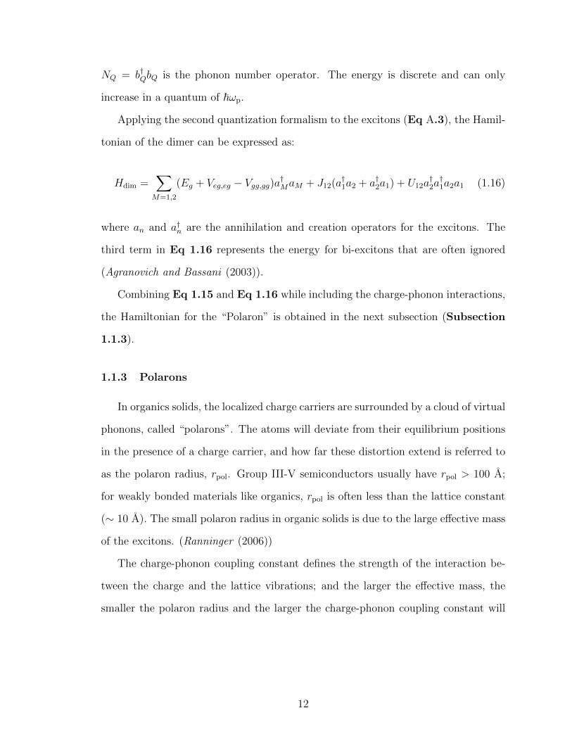
NQ = b†QbQ is the phonon number operator. The energy is discrete and can only
increase in a quantum of ~ωp.
Applying the second quantization formalism to the excitons (Eq A.3), the Hamil-
tonian of the dimer can be expressed as:
Hdim =∑M=1,2
(Eg + Veg,eg − Vgg,gg)a†MaM + J12(a†1a2 + a†2a1) + U12a†2a†1a2a1 (1.16)
where an and a†n are the annihilation and creation operators for the excitons. The
third term in Eq 1.16 represents the energy for bi-excitons that are often ignored
(Agranovich and Bassani (2003)).
Combining Eq 1.15 and Eq 1.16 while including the charge-phonon interactions,
the Hamiltonian for the “Polaron” is obtained in the next subsection (Subsection
1.1.3).
1.1.3 Polarons
In organics solids, the localized charge carriers are surrounded by a cloud of virtual
phonons, called “polarons”. The atoms will deviate from their equilibrium positions
in the presence of a charge carrier, and how far these distortion extend is referred to
as the polaron radius, rpol. Group III-V semiconductors usually have rpol > 100 A;
for weakly bonded materials like organics, rpol is often less than the lattice constant
(∼ 10 A). The small polaron radius in organic solids is due to the large effective mass
of the excitons. (Ranninger (2006))
The charge-phonon coupling constant defines the strength of the interaction be-
tween the charge and the lattice vibrations; and the larger the effective mass, the
smaller the polaron radius and the larger the charge-phonon coupling constant will
12
be. The Frohlich charge-phonon coupling constant, g, is written as,
g =e2
εpol
√m∗
2~3ωLO
(1.17)
where εpol is the dielectric constant of polaron and m∗ is it effective mass, ωLO is the
longitudinal optical phonon frequency.
Once the exciton, phonon and charge-phonon coupling are all well-defined, the
Hamiltonian of the polaron yields,
Hpol =∑MN
JMNa†MaN +
∑Q
~ωQ(b†QbQ +1
2) +
∑MQ
~ωQgQMM(b†Q + bQ)a†MaM (1.18)
where the first term in Eq 1.18 is the dipole interaction, generalized from the second
term in Eq 1.16; the second term in Eq 1.18 is the Hamiltonian for the phonons (Eq
1.15); the last term is the charge-phonon interaction, where (b†Q + bQ) is the phonon
displacement operator and gQMM is the charge-phonon coupling constant between M -
th exicton and Q-th phonon (Eq 1.17). Starting with this complicated Hamiltonian,
“thermal” factors in organic charge transport are discussed.
1.1.4 “Thermal” Factors
The experimental explorations on the organic charge mobility showed different
temperature dependence for crystalline and disordered organics. In Warta and Karl
(1985), a decrease in mobility with temperature in crystalline ultrapure naphthalene
was observed. In contrast, the temperature dependence was the opposite in Veres
et al. (2003): the hole mobility decreased with the inverse of the temperature in
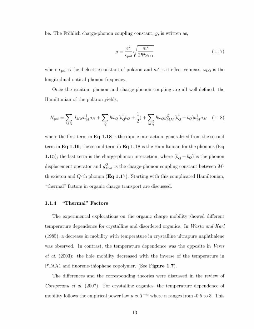
PTAA1 and fluorene-thiophene copolymer. (See Figure 1.7).
The differences and the corresponding theories were discussed in the review of
Coropceanu et al. (2007). For crystalline organics, the temperature dependence of
mobility follows the empirical power law µ ∝ T−α where α ranges from -0.5 to 3. This
13

dependence can be understood as that the relaxation time τe (in Eq 1.1) decreases due
to increasing phonon scattering at high T . Another approach to explain the inverse
relation starts with the narrow band nature of the organics: since the band width
is comparable to the thermal energy, kBT at 300K, the coherent charge transport is
disrupted by the thermal energy under room temperature. The coherent part of the
mobility can be written following the Boltzmann transport equation:
µcoh =
√πeτe
2NckBT
∫k
nk(1− nk)(v∗)2dk (1.19)
where Nc is the number of the charge carriers, nk is the Fermi-Dirac or Bose-Einstein
distribution depending on the charge of the particles. v∗ is the group velocity derived
from m∗.
Strong charge-phonon coupling and the impurities in the crystals both create
“traps”. If the depth of these traps is larger than kBT , the coherent transport will
be hindered. Therefore, in highly disordered systems, charge transport is phonon-
assisted and proceeds via hopping. The temperature dependence of the hopping
transport follows Arrhenius-like law:
µhop ∝ exp(−∆/kBT ) (1.20)
where ∆ is the activation energy that increases with the disorder level. Other methods
like Monte-Carlo simulation (Bassler (1993)) produce different temperature depen-
dence, such as
µhop,MC ∝ exp(−Tdis/T )2 (1.21)
µhop,MC is the Monte-Carlo simulated mobility, where Tdis represents the disorder.
An extensive discussion of the polaron model is presented in Appendix B,
adapted from Ortmann et al. (2009). The modeling results are shown in Figure
14
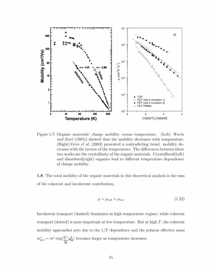
Figure 1.7: Organic materials’ charge mobility versus temperature. (Left) Wartaand Karl (1985)) showed that the mobility decreases with temperature.(Right)Veres et al. (2003) presented a contradicting trend: mobility de-creases with the inverse of the temperature. The differences between thesetwo works are the crystallinity of the organic materials. Crystallized(Left)and disordered(right) organics lead to different temperature dependenceof charge mobility.
1.8. The total mobility of the organic materials in this theoretical analysis is the sum
of the coherent and incoherent contribution,
µ = µcoh + µinc (1.22)
Incoherent transport (dashed) dominates in high temperature regime, while coherent
transport (dotted) is more important at low temperature. But at high T , the coherent
mobility approaches zero due to the 1/T dependence and the polaron effective mass
m∗pol = m∗ exp(∑Q
g2Q) becomes larger as temperature increases.
15

The incoherent mobility at low T is negligible, because,
µinc,low ∼g2Q
Te−~ωQ/kBT (1.23)
and at high T , the incoherent mobility yields,
µinc,high ∝ T−3/2e−Epol/kBT (1.24)
this effect is also referred to as self-trapping and the polaron energy is the reorgani-
zation energy of the molecules which can be written as
Epol =1
2g2Q~ωQ (1.25)
where gQ is the charge-phonon coupling constant of phonon mode Q; ~ωQ is the
energy of the phonon in this mode.
Note that, the charge-phonon coupling is a crucial parameter for organic charge
transport (See Figure 1.8) and the phonon energy can affect the charge transport
as well. However, there were no adequate study on the thermal properties and the
phonon dynamics for organic materials, and this missing knowledge will be discussed
in Ch. III and Ch. V.
In conclusion, charge and heat transport are interconnected. Thus, it is vital
to characterize the thermal properties of thin-film phase organics in order to better
understand the performance of organic-based devices at the molecular level.
1.2 Systematic Thermal Analysis
Thus far, the discussion has been confined to the thermal effects at microscopic
level. In this section, the heating effects are considered macroscopically.
The great demand for smaller, faster and more efficient electronic devices has led
16

Figure 1.8: Theoretical calculation of charge mobility of organics from Ortmann et al.(2009). The solid lines represent the total charge mobility. The coherent(dotted lines) and incoherent (dashed lines) contributions are also plotted.The mobility strongly depends on the electron-phonon coupling constantg, which is referred to as gQ in this thesis.
to a higher power consumption density. For example, the power density Pmp of a
microprocessor is written as
Pmp = NCV 2f (1.26)
where N is the number density of the devices, f is the operating frequency and C
and V are the capacitance and the voltage of the operating device. Higher N and f
result in a higher power dissipation and higher heat generation.
Figure 1.9 (left) is a picture of the Google data center in North Carolina. The
servers in the room are operating year-around and producing a huge amount of waste
heat and considerable effort has been made to redirect and utilize this waste energy. In
this Google data center, a massive water cooling system (Figure 1.9 (right)) is driving
the excess heat away, which prevents the overheating of the crucial components in
the servers. Similar data centers have been reported to redirect heat to the nearby
households, offices, swimming pools and greenhouse. Considerable research efforts
17

Figure 1.9: Data centers consume huge amounts of electricity, estimated to beup to 1.5 percent of all the world’s electricity. The left imageshows the google data center at North Carolina. However, prodi-gious amount of the electricity is dumped as heat. If it is not forthe water cooling plants (Right), the temperature accumulations cancause overheating problems to the crucial components. (Figure fromthe web: http://mpictcenter.blogspot.com/2012/10/google-throws-open-doors-to-its-top.html.)
focus on heat management at the environmental level, but their overview is beyond
the scope of this thesis. The focus of my work is the thermal management and analysis
at device and packing levels.
Analysis at the device level includes the estimation of how much heat is generated
inside the device and how long the device can operate. Increasing power density and
current levels, as mentioned before, generates more heat and this overheating can be
catastrophic to the electronic devices. The device temperature has to be maintained
at a reasonable level to prevent thermal failure and to extent the operation lifetime.
Therefore, the heat is directed out of the device and handled at the packaging level:
advanced packaging materials must have enough thermal dissipation power and micro-
cooling devices are often integrated into the electronic packaging. One of the micro-
cooling device, TE device, will be introduced in Section 1.3.
18

1.2.1 Heating in Organic Light-Emitting Diodes
The rest of Section 1.2 discusses the thermal analysis of Organic Light Emitting
Diodes (OLED). The amount of the temperature increase in a conventional LED is
written as (Efremov et al. (2006))
∆T = (1− ηeff)WkthdLED/ALED (1.27)
where ∆T is the amount of the temperature increase, ηeff is the efficiency of the
LED, W is the driving power, kth is the effective thermal conductivity and dLED,
ALED are the device thickness and active area, respectively. In the case of organic
LEDs, whose sample structure is shown in Figure 1.10 (Agrawal et al. (2013)), the
total thickness of the active layers is less than 200 nm while the substrate thickness
is a thousand times larger. Therefore, it is the thermal properties of the substrate
and packaging materials that most affect the temperature build-up in the device.
Chung et al. (2009) demonstrated the substrate’s effect on heat dissipation in OLED,
see Figure 1.11. Heat dissipation is more efficient for OLED on silicon substrate
than the same device on other low thermal conductivity substrates, such as glass and
stainless steel. However, glass is the most common substrate for OLEDs due to its
transparency. The temperature increase of OLED on glass is significant: T rises to 65
C after a 3-minute operation. Further increase of the device temperature can cause
degradation of the thin-film organics and result in the device failure. Adamovich et al.
(2005) showed the critical temperature of operation (120 C) for two specific types of
OLED (Red RD61 and Green GD33).
As mentioned above, Eq 1.27 indicates that the organic layers in OLED are so
thin that they barely contribute to the temperature increase. Here, I present a simple
simulation of the heat dissipation in OLED active layers, showing the speed of the
thermalization process inside these organic layers. The simulation follows transient
19

Figure 1.10: Materials was deposited onto glass substrate using VTE. From bottomto top: Al (40 nm)/ NiO (4 nm)/α−NPD (50 nm)/Alq3 (60 nm)/Al:LiF(2.5 nm)/Ag (20 nm). (Figure from Agrawal et al. (2013))
Figure 1.11: IR images of the temperature profile of the operating OLEDs on differentsubstrates. Substrate: Glass (Top); Substrate: Stainless Steel (Middle);Substrate: Silicon (Bottom). (Figure from Chung et al. (2009))
heat conduction equation
kth∇2T + qth = CpdT
dt(1.28)
where Cp is the heat capacity at constant pressure and qth is the heat flux related to
the current density and the device efficiency. Applying Eq 1.28 to the OLED struc-
ture in Figure 1.10 while assuming the heat generation is confined in organic active
layer (aluminum hydroxiquinoline (Alq3)) with rate of 1 W/cm2, the temperature pro-
file is calculated and the results are shown in Figure 1.12. The temperature at the
top surface, which is exposed to the ambient, rises quickly to match the temperature
of the active layer within 1 ns; due to the low thermal conductivity of the organic hole
20
Figure 1.12: Transient temperature profile of the OLED in Figure 1.10 modeled at0s, 60fs, 450 ns. Thermalization within the organic layers is less than 60fs. (Figure by Yansha Jin)
transport layer N,N’-di-1-naphthyl-N, N’- diphenyl-1, 1’-biphenyl-4, 4’diamine (NPD)
and the glass substrate, the thermalization process at the bottom side is comparably
slower. In less than 1 µs, the temperature distribution in the organic layers becomes
nearly uniform. Thus, if one is interested in investigating the microscopic “heating”
processes in the organics, the time resolution should be several nano-seconds.
However, the thermal conductivity of organic layers is still crucial for OLEDs,
especially when analyzing nano-scaled features. One major advantages of organic
materials lies in the large-area lighting applications. However, as the size of the OLED
increases, the “hot spots” become unavoidable. The hot spots originate from the
rough surface of the substrate, even a tiny spike can cause current crowding and local
heat generation (Park et al. (2011)). The localized current injection was also observed
in nanoscale light sources (Zhao et al. (2007)), where OLED was deposited onto an
Atomic Force Microscopy (AFM) tip. Shown in Figure 1.13, heat accumulates at
the tip due to the high local current density, and the organic materials melted after
the standard operation.
The breakdown mechanism of nanoscale features such as hot spots, edges and
21

Figure 1.13: Thermal failure of non-planar OLED causing by local joule heating.SEM images of the organic heterostructure device on AFM probe tipbefore and after normal operation; The region at the center of the tipmelted and imaged at 2× magnifications; The intense joule heating atthis region is due to the tip geometry. (Figure from Zhao et al. (2007))
tips is closely related to the thermal conductivities of the organic layers. Thus, the
characterization of thermal conductivity of these organic semiconductors in thin-film
phase is crucial for analyzing the device performances.
1.3 Thermoelectrics
Two problems originated from the excessive heating in electronic devices have
been briefly discussed in the previous section (Section 1.2) : how to cool down the
devices and how to manage the waste heat. The use of TE devices can be the solution
to both because of their ability to convert temperature gradients into voltage, and
can also realize the conversion in a reverse direction.
1.3.1 Thermoelectric Effects
To cool down a hot component using a thermoelectric device, one can apply a
voltage to create a temperature difference. This phenomena is called thermoelectric
cooling effect, also known as Peltier effect. The image of a commercial Peltier cooler
is shown in Figure 1.14. A temperature difference can be generated between the top
and the bottom side of the device with the applied voltage, causing heat extraction
from the cold side to the hot side. Attaching the electronic device to the cold side,
22

Figure 1.14: The working principle and the schematic drawing of the Peltier cooler.The image on the left shows the real design of a Peltier cooler. Theright image shows the working principle by drawing the Seebeck circuit.“The Peltier effect is the presence of heating or cooling at an electrifiedjunction of two different conductor” - defined by Wikipedia. (Left imagefrom the web: http://www.kryotherm.ru/?tid=23 and Right image fromSnyder and Toberer (2008))
the heat generated in the device can be directed out. In this way, the device can be
maintained at its normal operating temperature.
To manage the waste heat, one can scavenge the unused heat to create a “hot
side”: the temperature difference converts to electricity within the TE device. This
conversion is the well-known Seebeck effect and the corresponding devices are often
referred to as the thermoelectric generators.
Despite how promising the principle seems to be, challenges remain in making the
thermoelectric devices more efficient and cost-effective.
1.3.2 Efficiency of Thermoelectric Devices
The relation between the temperature difference, ∆T = Th − Tc, (Th, hot side
temperature and Tc, cold side temperature), and the electric voltage, ∆V , is written
as
∆V = −S∆T (1.29)
23

Figure 1.15: TE efficiency versus temperature with various of ZT . The maximum ef-ficiency of thermoelectric device increases with ZT . (Figure from Yadav(2010))
where S is the thermopower, also known as Seebeck coefficient. The maximum effi-
ciency for a thermoelectric generator is
ηmax = (1− ThTc
)
√1 + ZTavg − 1√1 + ZTavg + Tc
Th
(1.30)
where Figure of Merit (ZT) is
Z =σeS
2
kth
(1.31)
and Tavg = 12(Tc + Th). The relation between ηmax and Th at different ZTavg is
plotted in Figure 1.15 (Yadav (2010)) while setting Tc to be room temperature. It
is evident that material with a larger ZTavg can make better TE devices at the same
operating temperature Th. Usually, a material that exhibits ZTavg ∼ 1 is considered
as a promising candidate for TE.
To obtain a larger ZTavg, a larger S, a smaller kth and a large σe are desired.
However, this is a conflicting combination of material properties (Snyder and Toberer
(2008)).
24
The Seebeck coefficient S for metals or degenerate semiconductors is given by:
(Cutler et al. (1964))
S =8π2k2
B
3eh2m∗T (
π
3n)2/3 (1.32)
where m∗ is the effective mass of the carrier and n is the carrier concentration. Small
n benefits the thermopower, S. A large electrical conductivity, however (See Eq
1.1), requires a large n. Moreover, kth often increases with σ. The electron (charge)
contribution to thermal transport kth,e in Eq 1.11 is directly related to σ,
kth,e = σLwfT (1.33)
where Lwf is the Lorenz factor. Lwf is 2.4×10⁻⁸ J2K−2C−2 for the free electron (Sny-
der and Toberer (2008)). Achieving the combination of the desired material proper-
ties seems to be a mission impossible for conventional materials, but the nanoscale
manipulation of materials’ structure provides many novel pathways to overcome this
difficulty. Moreover, ZT will not remain constant while temperature changes, Figure
1.15 is just an unrealistic illustration. ZT ’s relation versus the temperature of several
materials is shown in More details on the nanostructure manipulation to increase ZT
will be discussed in Ch. IV.
1.3.3 Organic Thermoelectrics
Organic materials have low thermal conductivity kth and large effective mass m∗
intrinsically that are both desired for TE materials. One of the major problematic
properties is its low electrical conductivity, σe. Highly conductive polymers and
organic semiconductors with higher σe were investigated for the potential in making
TE devices. With the scalability and the affordable price of the organics, cost-effective
TE devices for the large-scale heat harvesting can be realized potentially.
kth plays an important role in the efficiency of thermoelectric materials, as can
25

Figure 1.16: ZT versus temperature for several materials. (Figure from Minnich et al.(2009))
be seen in Eq 1.31. But no adequate study has explored the thermal properties
of organic semiconductors and research on organic thermoelectrics is not mature.
Recently, many interesting studies have presented some promising results for organic
TE (Kim et al. (2011); Wang et al. (2009)) and proposed ways to optimize ZTavg in
organics (Bubnova et al. (2011); Aıch et al. (2009)).
In this thesis, the measurements and discussions on the thermal conductivity of
organic semiconductors and organic/inorganic hybrids, along with novel ideas for the
next generation organic thermoelectric devices are presented. (Refer to Ch. III, Ch.
V and Ch. IV)
1.4 Organization of the Thesis
Thermal properties of the disordered organic solids are crucial for researching
the charge transport and the mobility characterization of the organic semiconductor;
26
also crucial for the thermal analysis of the thin-film organic electronic devices and
the performance of organic thermoelectric devices. Despite the importance of the
research, there has yet to be a complete study on the thermal properties of organics
and its hybrids with the inorganics. In this thesis, organic thermal conductivities
are measured and interesting facts of the interfacial contribution at organic/metal in-
terfaces are discovered. The boundary/interfacial contribution to the thermal trans-
port cannot be neglected in thermal analysis of nanostructured organic optoelec-
tronic/thermoelectric devices. Especially for thermoelectric devices, the boundary
effect can assist in enhancing the figure of merit in organic/metal nanocomposites.
The fundamental physics of this boundary effect is also discussed.
The organization of the thesis is as follows,
Chapter II gives a review on the thin-film thermal properties measurement tech-
niques, focusing on the technique used for this work, the 3-ω method.
Chapter III reports the results of the thermal conductivity measurements on
organics and organic/metal hybrids. The concept, thermal boundary conductance, is
introduced and its significance in organic/metal systems is presented.
Chapter IV continues the discussions on the boundary effect with a focus on the
impact to the thermoelectric material design.
Chapter V and Chapter VI focuses on the fundamentals of the thermal bound-
ary conductance at the interfaces involving organics, along with an extensive discus-
sion on the existing analytical and computational modeling techniques.
The final chapter, Chapter VII presents the summary for the present work and
further research directions.
27
CHAPTER II
Methods for Thin-Film Thermal Property
Measurements
The unit of thermal conductivity kth is W/mK, suggesting that kth is the trans-
mitted power under a temperature gradient per unit thickness,
kth =d
A
q
∆T(2.1)
Eq. 2.1 is the governing equation for the thermal conductivity measurement: for a
sample with a known dimension, its thermal conductivity can be calculated from the
measured quantities: the driven power q and the temperature difference ∆T .
Figure 2.1 shows the giant apparatus for thermal conductivity measurement in
1967. This early apparatus was based on steady-state method, with the sample is at
the equilibrium state. The main disadvantages of the steady-state method are the
long time to reach equilibrium and the radiative energy loss at room temperature.
These disadvantages can be avoid in the transient measurements. Well-known
transient measurements include the 3-ω method and the Time-Domain Thermore-
flectance (TDTR) method. 3-ω method is simpler to operate and cost-effective;
TDTR is a non-contact method based on the pump-probe technique. Both these
methods are discussed in detail in the following sections (Section 2.1 and Section
28
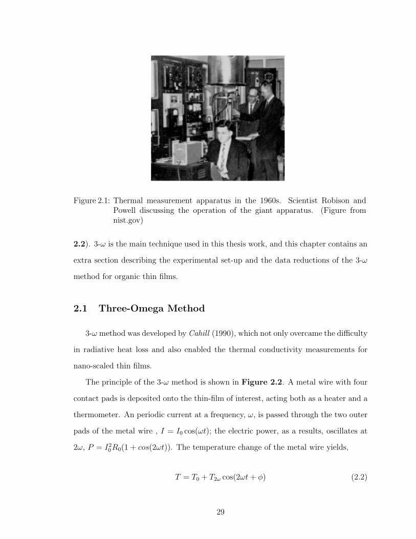
Figure 2.1: Thermal measurement apparatus in the 1960s. Scientist Robison andPowell discussing the operation of the giant apparatus. (Figure fromnist.gov)
2.2). 3-ω is the main technique used in this thesis work, and this chapter contains an
extra section describing the experimental set-up and the data reductions of the 3-ω
method for organic thin films.
2.1 Three-Omega Method
3-ω method was developed by Cahill (1990), which not only overcame the difficulty
in radiative heat loss and also enabled the thermal conductivity measurements for
nano-scaled thin films.
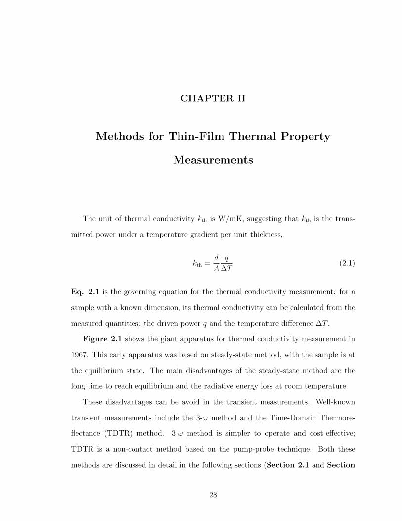
The principle of the 3-ω method is shown in Figure 2.2. A metal wire with four
contact pads is deposited onto the thin-film of interest, acting both as a heater and a
thermometer. An periodic current at a frequency, ω, is passed through the two outer
pads of the metal wire , I = I0 cos(ωt); the electric power, as a results, oscillates at
2ω, P = I20R0(1 + cos(2ωt)). The temperature change of the metal wire yields,
T = T0 + T2ω cos(2ωt+ φ) (2.2)
29

Figure 2.2: Schematic Illustration of 3-ω method for thermal conductivity measure-ments. (Left) The thin film is deposited onto a planar substrate anda metal wire with four contact pads is deposited atop of the thin film.The exact design of the metal wire is l = 4mm and 2b = 80µm; Simplyillustration of the principle of the 3-ω method for thermal conductivitymeasurements is presented in the right image: A periodic current withfrequency ω is passed through the two outer contact pads, the electricpower is oscillating at double the frequency. The temperature rise in thewire correlates to the power and kth of the film of interest and also ownsa frequency of 2ω. However, the temperaure rise (T2ω) is too small todetect accurately; so instead probing the temperature signal, 3-ω methodmeasure the voltage signal between the two inner pads which containsthe information of T2ω. Voltage signal can be amplified by lock-in am-plifier and measured at higher frequency. (Figure by Yansha Jin and Dr.Abhishek Yadav)
30

where φ is the phase shift. This temperature fluctuation correlates to the thermal
conductivity of the thin film underneath the metal wire. With a small temperature
fluctuation, T2ω ∼ 5K, the resistance of metal reacts linearly to the temperature,
R = R0 +R0CrtT2ω cos(2ωt+ φ) (2.3)
where R is the resistance, R0 is the initial resistance; and Crt is the resistance tem-
perature coefficient, which is written as,
Crt =∆R
R0∆T(2.4)
As a result, the voltage probed from the two inner pads yields,
V = IR = I0 cos(ωt)(R0 +R0CrtT2ω cos(2ωt+ φ)) (2.5)
= I0R0 cos(ωt) + I0R0CrtT2ω1
2(cos(3ωt+ φ)− cos(ωt+ φ))
= Vω cos(ωt+ φ′) + V3ω cos(3ωt+ φ)
For nanoscaled thin films, the temperature fluctuation T2ω is too small for direct
measurements. 3-ω method provides a way to transfer this temperature signal to a
voltage signal, V3ω, which can be amplified using a lock-in and detected at a higher
accuracy.
The temperature fluctuation can be extracted from the experiment using the mea-
sured quantities,
T2ω =2V3ω
I0R0Crt(2.6)
However, this fluctuation’s relation to the thermal conductivity is much more com-
plicated than Eq 2.1 considering a 3 -D film with a line heater. Following the Fick’s
31
law and the Fourier’s law, T2ω yields (Cahill (1990)),
T2ω =P
lπkth
∞∫0
sin2(kb)
(kb)2(k2 + q2)1/2dk (2.7)
where 2b is the width of the metal line heater; q is the penetration depth, defined as,
q = (κ/2iω)1/2 (2.8)
where κ is the thermal diffusivity,
κ =kth
ρCv(2.9)
Under the condition |qb| 1, the temperature fluctuation calculated from the heat
conduction model Eq 2.7 can be approximated as,
T2ω =P
2πlkth
[ln(κ
b2)− ln(2ω)]− i P
4lkth
= Tin−phase + Tout−phase (2.10)
Comparing Eq 2.7 and Eq 2.6, the temperature fluctuation from a periodic
current load can be measured and calculated. The calculation has only one sensible
parameter, the thermal conductivity of the film, kth. Figure 2.3 shows the in-
phase T2ω for a 45 nm SiO2 film deposited on Si substrate (Lee and Cahill (1997)).
The markers are the experimental values while the curves represent the Tin−phase
calculated using SiO2’s thermal conductivity. The agreement between experimental
and calculation confirms the validity of the 3-ω method for kth measurements.
Recall that steady-state methods are not applicable at room temperature due to
32

Figure 2.3: An example data analysis of 3-ω measurement. In-phase T2ω calculatedfrom V3ω for a 45 nm SiO2 film on Si substrate. (Figure from Lee andCahill (1997))
the large radiative loss. In 3-ω method, the radiation heat loss is,
Grad ' 2σεT 3(2A) = 2σεT 3(2l|1/q|) (2.11)
the total heat generation rate is G ' lkth and the radiation error of 3-ω method
yields,
Grad/G ∼ |1/q|T 3 (2.12)
Generally, if |1/q| < 100µm, the radiation error is negligible.
3-ω method has been shown to be accurate for many inorganic dielectric materials
and some organic semiconductors (Kim et al. (2005)). In this thesis, I will discuss in-
depth how to apply this method to more organic semiconductors and extend the study
to organic/inorganic hybrids. A detailed discussion of the 3-ω method for organics is
presented in the last section (Section 2.3) of this chapter .
33

Figure 2.4: Principle of TDTR thermal conductivity measurement. A pump pulse in-troduces local heating and temperature rises suddenly then exponentiallydecay during the interval of the pump pulses. The probe pulse followsto detect the instant change in reflectance caused by this local heating.(Figure from Schmidt et al. (2008) and adapted by Yansha Jin)
2.2 Time-Domain Thermo-Reflectance Method
Besides introducing temperature gradient using electrical heating like the 3-ω
method, supplying heat by laser beam is another promising alternative in thermo-
property measurements.
Time-domain Thermoreflectance (TDTR) is the method based on laser heating.
Picosecond or nanosecond laser pulses introduce the thermal energy to the thin films,
and the changes in the reflectance are then detected by time-delayed probe pulses.
The TDTR principle is shown in Figure 2.4 (a). A pump pulse causes the
local heating in the thin film structure, followed by a probe pulse to detect the
instant reflectance changes caused by the local heating. In Figure 2.4 (b) (Daly
et al. (2002)), the temperature profile of the film is presented (the blue line), T rises
instantaneously with the pump pulses and decays exponentially during the intervals,
∆T (t) ∝ exp(−t/τd), where τd =dfdsCvkth
(2.13)
in which df and ds are the thickness of the film and the substrate, respectively. The
34

Figure 2.5: CuPc thermal conductivity measurement by TDTR. The change re-flectance represents the temperature fluctuation; the best fitting yieldsto kth,CuPc = 0.34 W/mK. (Figure from Sun (2013))
signals probed are plotted in the black line, the change in the reflectance is directly
correlated to ∆T . Thermal conductivity can be extracted by fitting the calculated ∆T
by 3-D heat conduction model (Cahill (2004)) to the measured temporal temperature
profile.
Details on TDTR measurements of organic kth can be found in Sun (2013). Mea-
surement result for CuPc is presented in Figure 2.5, kth is 0.34 W/mK. The fitting
is very sensitive to the value of kth and the error-bar is smaller than 10%.
Compared with the 3-ω method, TDTR is more versatile. For example, the strain-
echoes contains information of materials’ sound velocity; besides, using GHz pulses
in this pump and probe techniques can excite coherent acoustic modes in the samples
which enables the study on other interesting physics and applications, such as acoustic
cavity (Sun et al. (2013)).
However, the experimental apparatus for TDTR is more complicated and expen-
sive compared to that of the 3-ω method. If the work is only confined to thermal
conductivity measurements for organics, like in this thesis, 3-ω method is preferred
35

Figure 2.6: Experimental set-up for 3-ω method for the work in this thesis. (a) Topview of the heating wire on top of the film imaged by optical microscopy.(b) Sample was put on a glass slide as adiabatic bottom with a copperblock and a Peltier cooler underneath. A heat sink and a fan are attachedat the bottom. (c) Schematic cross-section view of the sample structure.Film is deposited on the undoped silicon substrate and placed on a glassslide. (d) Circuit design. (Figure adapted from Jin et al. (2012))
due to its simplicity and the satisfactory accuracy of the measurements.
2.3 Three-Omega on Organic Thin Film
In this section, the details on 3-ω measurements of organics are presented, includ-
ing its limitations and technical difficulties, experimental set-up, sample preparation
and data reduction details.
Borca-Tasciuc et al. (2001); Tong and Majumdar (2006) are excellent review pa-
pers for the 3-ω method. Effects of anisotropy, substrate-film thermal conductivity ra-
tio, heater capacitance and substrate-film interface conductance have been discussed.
The paper also compared differential and slope methods and the data reduction for
the multilayer film structure.
36

For organic thin films, the thermal conductivity is 100 times smaller than that
of the Si substrate; and the heater capacitance and the substrate-film interfacial
conductance effect is negligible. Besides, there is no anisotropy to consider in the
disordered organic films. Thus, the major limitation in testing organic semiconductor
thin films and their hybrids with metals is the high electrical conductance of the film
which might cause the parasitic current.
In order to minimize the parasitic current, highly resistive Si substrate (ρs >
10000 Ω cm) is used. Moreover, for conductive thin films, such as CuPc/Ag hybrids,
an electrically insulating capping layer is essential to be on the top of the film stack,
in order to eliminate the unwanted leakage current.
The experimental set-up is shown in Figure 2.6. Figure 2.6 (a) shows the
film with the metal heating wire; Figure 2.6 (b) is the photo of the probe station;
Figure 2.6 (c) shows the schematic sample structure, the whole sample was placed
on glass slide which is treated as an adiabatic bottom boundary; Figure 2.6 (d) is
the drawing of the experimental circuit design by Dr. Abhishek Yadav.
If the thin-film entity contains multiple layers, the heat conduction modeling for
such film is slightly modified from Eq 2.7 (Borca-Tasciuc et al. (2001)),
∆T = − P
πlkth,1
∞∫0
1
A1B1
sin2(bk)
b2k2dk (2.14)
where
Ai−1 =Ai
kth,iBi
kth,i−1Bi−1− tanh(Bi−1di−1)
1− Aikth,iBi
kth,i−1Bi−1tanh(Bi−1di−1)
, i = 2 . . . n, (2.15)
Bi = (k2 +i2ω
κi)1/2 (2.16)
In the above expressions, subscript i represents the i-th layer starting from the top
surface. Following these relations, the temperature change can be calculated by dif-
ferent kth input, then compared with the experiment to extract the most accurate
37

Figure 2.7: Data reduction of 3-ω thermal conductivity measurement of CuPc film onundoped Si. (a) In-phase and out-of-phase T2ω calculated from Eq 2.14and measured by lock-in amplifier; the transformation of the measuredvoltage signal to the temperature signals follows Eq 2.6 (b) Measurementof temperature coefficient of resistance. The four point-probe resistanceof the wire changes linearly with the temperature near room temperature.(Figure adapted from Jin et al. (2011))
kth.
In the measurements, the V3ω is recorded by a lock-in amplifier; the resistance R0
is measured using a multimeter; I0 is the known and adjustable current source. Crt
value is obtained by measuring the wire resistance under a series of temperatures near
the room temperature. Figure 2.7 presents a typical fitting of kth and an example
of Crt data reduction.
The experimental values of the thermal conductivity in following chapters are
obtained by the 3-ω technique. Further discussion on measurements on conductive
samples, such as organic/metal multilayers will be discussed in Section 3.6.
38
CHAPTER III
Thermal Boundary Conductance at Organic-Metal
Interfaces
3.1 Introduction: a Significant Boundary Contribution
Research interest in the thermal properties of organics was discussed in Ch. I.
With the ability to measure the thermal conductivity, kth (See Ch. II), kth values
of several organic semiconductors in the thin-film phase were measured using the 3-ω
method. Jin et al. (2011); Kim et al. (2005). The room temperature kth of these
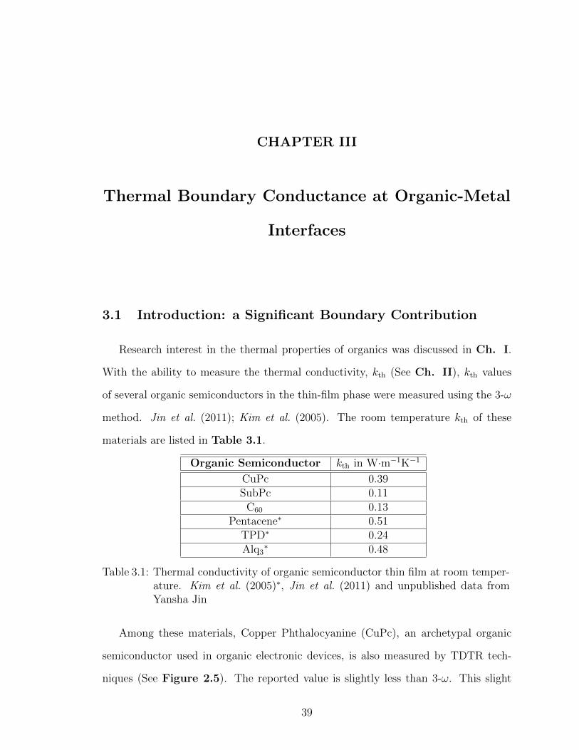
materials are listed in Table 3.1.
Organic Semiconductor kth in W·m−1K−1
CuPc 0.39SubPc 0.11
C60 0.13Pentacene∗ 0.51
TPD∗ 0.24Alq3
∗ 0.48
Table 3.1: Thermal conductivity of organic semiconductor thin film at room temper-ature. Kim et al. (2005)∗, Jin et al. (2011) and unpublished data fromYansha Jin
Among these materials, Copper Phthalocyanine (CuPc), an archetypal organic
semiconductor used in organic electronic devices, is also measured by TDTR tech-
niques (See Figure 2.5). The reported value is slightly less than 3-ω. This slight
39

reduction is due to the interfacial thermal resistance at the film-substrate interface.
Interfacial contribution to the thermal transport in nanostructures have proved to be
significant and very useful in various of applications, such as data storage elements
and thermal barrier coating (Peng et al. (1997); Kim et al. (2000)). Recently, ultralow
thermal conductivity for the thermal barrier coating was achieved in metal/dielectric
multilayer films because of the large interfacial thermal resistance. Likewise, thermal
transport across dissimilar (i.e., organic/metal) interfaces can play a role in the un-
derstanding and the operation of organic optoelectronic devices, where organic/metal
junction widely existed. While packaging often dominates heat dissipation in such
devices, as mentioned in Subsection 1.2.1, the nanoscale heat transfer can be im-
portant in analyzing smaller features, such as hot spot, edges and tips. Moreover, the
charge transport is closely related to thermal transport Section 1.1. Thus, exploring
the interfacial thermal transport can be beneficial to the understanding of the charge
injections from metal electrodes to organic active layers.
The next logical question to ask is “Is the interfacial resistance at organic/metal
interfaces significant enough to make a difference?”. and the answer is “Yes”.
The thermal conductivities of three nanostructured films were measured. The
first sample was a single CuPc film; the second sample was a co-deposited CuPc and
Ag film with a 50% volume fraction of each; the third sample was an alternating
multilayer structure consisting CuPc and Ag, with layer thickness, tCuPc = tAg. Thus
the volume fraction of Ag was also 50% in the third sample, same as the second
sample.
kth of the Vacuum Thermal Evaporated (VTE) CuPc film is 0.39 ± 0.04 W/mK
and its surface morphology is shown in Figure 3.1 (a). This Transmission Electron
Microscopic (TEM) image was taken by JEOL 2010, imaging the CuPc film deposited
on a copper TEM grid covered by holy carbon film.
Metals like silver are thermally conductive. kth of silver is 439 W/mK, thus the
40

Figure 3.1: TEM images and schematic drawings of (a) Single layer of CuPc filmon Si (b) Film of the mixture of CuPc and Ag on Si, with Ag volumefraction 50%; (c) Three-period multilayers of CuPc/Ag, with identical Agand CuPc layer thickness, thus the silver volume fraction is also 50%).(Figure from Yansha Jin)
second sample, the mixture of Ag and CuPc, was measured to possess a kth of 1.3
± 0.28 W/mK by the 3-ω method. This structure was also deposited onto the TEM
grid and imaged by TEM, see Figure 3.1 (b). Silver formed nanoparticles that are
dispersed in the CuPc matrix.
However, the alternating multilayers with the same Ag volume fraction didn’t give
the rise to kth. Instead, a three-period CuPc/Ag multilayer structure with tCuPc =
tAg = 10 nm is measured to have kth = 0.19 ± 0.03 W/mK. Surprisingly, this value
is significantly less than the thermal conductivity of the single CuPc films. Such
multilayer systems containing interfaces between dissimilar materials exhibit lower
thermal conductivity than their pure constituents, indicating the significance of the
interfacial contribution to the thermal transport in nanoscale films.
The purpose of this chapter is to quantify the organic/metal interfacial contri-
bution to the thermal transport, known as Thermal Boundary Conductance (TBC).
41
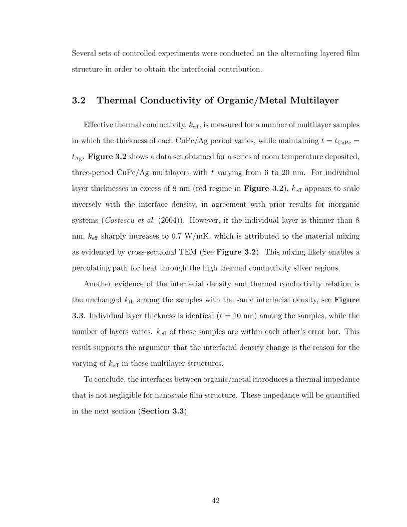
Several sets of controlled experiments were conducted on the alternating layered film
structure in order to obtain the interfacial contribution.
3.2 Thermal Conductivity of Organic/Metal Multilayer
Effective thermal conductivity, keff , is measured for a number of multilayer samples
in which the thickness of each CuPc/Ag period varies, while maintaining t = tCuPc =
tAg. Figure 3.2 shows a data set obtained for a series of room temperature deposited,
three-period CuPc/Ag multilayers with t varying from 6 to 20 nm. For individual
layer thicknesses in excess of 8 nm (red regime in Figure 3.2), keff appears to scale
inversely with the interface density, in agreement with prior results for inorganic
systems (Costescu et al. (2004)). However, if the individual layer is thinner than 8
nm, keff sharply increases to 0.7 W/mK, which is attributed to the material mixing
as evidenced by cross-sectional TEM (See Figure 3.2). This mixing likely enables a
percolating path for heat through the high thermal conductivity silver regions.
Another evidence of the interfacial density and thermal conductivity relation is
the unchanged kth among the samples with the same interfacial density, see Figure
3.3. Individual layer thickness is identical (t = 10 nm) among the samples, while the
number of layers varies. keff of these samples are within each other’s error bar. This
result supports the argument that the interfacial density change is the reason for the
varying of keff in these multilayer structures.
To conclude, the interfaces between organic/metal introduces a thermal impedance
that is not negligible for nanoscale film structure. These impedance will be quantified
in the next section (Section 3.3).
42

Figure 3.2: Thermal conductivity versus layer thickness of the three-period multilay-ers CuPc/Ag. Above 8 nm per layer, kth increases with layer thicknesswhile the volume fraction is kept the same, strongly suggesting the in-terfacial contribution to the thermal transport; Below 8 nm per layer,kth rapidly increases with decreasing layer thickness due to the mixingof CuPc and Ag. No layered structure is observed for 6 nm per layerfilm, shown in the cross-sectional TEM image at left; while the right im-age shows a CuPc/Ag multilayer with 20 nm per layered with distinctinterfaces between CuPc/Ag. (Figure adapted from Jin et al. (2011))
3.3 Thermal Boundary Conductance at Organic/Metal In-
terfaces
The impedance introduced by the interfaces leads to a temperature discontinuity
∆T in the presence of heat flux. The thermal boundary conductance (TBC) (Kapitza
(1941); Pollack (1969)) is defined as
Gb = q/∆T (3.1)
where ∆T is the temperature discontinuity and q (W/m2) is the applied heat flux.
To extract the numerical value of the organic/metal thermal boundary conduc-
43
Figure 3.3: Thermal conductivity of CuPc/Ag multilayer versus number of layerswhile keeping the layer thickness constant. The thermal conductivityslightly fluctuates because the interface densities are the same amongthis series of samples. (Figure from Yansha Jin)
tance Gb, a series of thermal resistances corresponding to the organic film, metal film,
and interface is presented:
NtCuPc
Akth,CuPc
+Ntth,MAkth,M
+n
AsGb
+1
AGbottom
=N(tCuPc + tM)
Akeff
(3.2)
where keff is the cross-sectional effective thermal conductivity of the whole multi-
layer structure, kth,CuPc and kth,M are the thermal conductivities of CuPc and the
metal, tCuPc and tM are the layer thicknesses; Gb is the TBC of CuPc/metal interface
and Gbottom is the TBC at the bottom metal/Si interface, n is the number of the
CuPc/metal interfaces, N is the number of periods of the alternating multilayers, A
is the cross-sectional area and As is the effective interface area measured by AFM.
A quartz crystal microbalance monitor with a system error of approximately 2% was
used during the deposition to keep the layers’ equal t = tCuPc = tM; AFM measure-
ments confirmed the film’s Root Mean Square (RMS) roughness to be approximately
2∼4 nm for a 15 nm thick film. For a three-period multilayer structure used in this
44

study, n = 5 and N = 3. Thus, Eq 3.2 yields:
A
Ast= 0.6 ·Gb(
2
keff
− 1
kth,CuPc
− 1
kth,M
− 1
3tGbottom
) (3.3)
A linear fit of the LHS versus the RHS of Eq 3.3 was used to derive Gb: the TBC
of CuPc/metal interfaces. Note that for the alternating layered systems, the phonon
interference generally needs to be considered (Hu et al. (2010)). However, because
the short phonon mean free path in CuPc films (1∼2 nm) is comparable to the RMS
roughness of CuPc/metal interfaces and much smaller than the layer thickness (∼10
nm), the phonons are no longer coherent. This suggests that the phonon interference
effects can be neglected in this study.
Figure 3.4: Thermal conductivity of CuPc thin film stays at 0.39 W/mK as filmthickness increases from 10 to 40 nm. (Figure from Jin et al. (2012))
Because my approach relies on varying the individual layer thickness, it is im-
portant to understand whether the thermal conductivity of a given layer can change
significantly with the variations in thickness. Experimental show that kth,CuPc does
not vary appreciably (only about 5% fluctuation) for films ranging between 10∼40
nm in thickness (See Figure 3.4), and consequently, the error introduced by possible
variations in kth,CuPc into the calculation of TBC is less than 5%. Moreover, kth,M is
45

1000 times larger than kth for the organic films, thus a physically realistic variation
in this term with thickness make little difference in the value of TBC extracted via
Eq 3.3.
Figure 3.5: Thermal boundary conductance values of CuPc/metal interfaces. Usingan equivalent circuit model for thermal conduction through the multilayerstack. TBC values are extracted from the slopes of the linear plot (theLHS and RHS of Eq 3.3). (Figure adapted from Jin et al. (2012))
Results of 3-ω measurements of thermal boundary conductance of CuPc/gold,
CuPc/magnesium, CuPc/aluminum and CuPc/silver interfaces are presented. Using
the modified Fourier’s law (Eq 3.3) with TBC as the additional term, the slope
of the linear fit of a series of samples with different interface densities is 1/Gb this
specific material system. Figure 3.5 shows the linear fits for all four CuPc/metal
combinations; the TBC values for the different interfaces were calculated from these
fits and listed in Figure 3.5 as indicated.
These values are lower compared to other metal dielectric interfaces, whose TBC
values are also listed in Table 3.2 along with the TBC of CuPc/metal interfaces.
46

Materials System Gb in MW·m−2K−1
CuPc : Ag 13 ± 3 †
CuPc : Al 50 ± 15 †
CuPc : Mg 40 ± 10 †
CuPc : Au 19 ± 5 †
Au : Si 145
Pt : Si 140
Cr : Si 180
Cr : sapphire 190
Cr : GaN 230
Cr : AlN 200
Al : Si 120
Al : sapphire 200, 105 ∗
Al : GaN 190
Al : AlN 230
Al : Si 120
Al : sapphire 200
Pb: sapphire 55 ∗
Au: sapphire 45 ∗
Table 3.2: Thermal boundary conductance of various of materials system. Stevenset al. (2005), Stoner and Maris (1993)∗, Jin et al. (2012)†
3.4 Effect of Morphology and Growth Conditions on Ther-
mal Properties of Organic Thin Films
Growth conditions influence the thermal properties of the film and the inter-
faces. CuPc films were deposited onto Si substrates at different substrate temper-
ature. Scanning Electron Microscopy (SEM) images show the surface morphology
of these films (See Figure 3.6). Thermal conductivities, kth, of the corresponding
films are presented along with the SEM images, and a drop in kth with decreasing
deposition temperature is observed. Another interesting phenomenon observed was
the cracking of the CuPc film below -60C due to the large mismatch of the thermal
expansion coefficient of the substrate and the CuPc film.
Beyond the critical temperature for film cracking, the low temperature deposition
can create smoother films. AFM images revealed that films deposited at -60 C are
47

Figure 3.6: Thermal conductivities and the surface morphology of CuPc thin filmson Si substrates, with the deposition temperature varying. (Figure fromYansha Jin)
smoother, with root-mean-square roughness values and grain sizes four times smaller
than those of the RT-deposited films (See Figure 3.7). The influence on interface
mixing on TBC can be further assessed by comparing the RT results to those for
samples deposited onto colder substrates, since these latter samples have interfaces
which are more distinct. As shown in Figure 3.8, we measure lower effective thermal
conductivities for CuPc/Ag multilayers deposited at -60 C than for pure CuPc films
deposited at -60 C (0.32 W/mK), implying that the TBR of CuPc/Ag interfaces
remains a major contributor to the overall thermal resistance. Because the interfaces
in the -60 C samples are sharper than those in the 20 C samples at the same layer
thickness, the thermal conductivities of the former samples are generally lower than
those of the latter samples. Similar trends in keff with layer thickness were observed
for three-period CuPc/Al multilayers as shown in Figure 3.8.
48

Figure 3.7: Surface and interface morphology of RT and CT CuPc and CuPc/Al thinfilms. Upper images are taken by AFM: 50 nm CuPc are deposited at 20C and -60 C; the RMS roughnesses for RT deposited sample is 4.48 nm,and CT deposited sample is 0.78 nm; Bottom images are taken by TEM:these cross-sectional images of CuPc/Al layers show that RT deposited Alon CuPc has larger interfacial regime, ∼ 10 nm. (Figure from Jin et al.(2011))
3.5 Confirmation of Thermal Conductivity Measurements by
Molecular Dynamics Simulations
Thermal conductivities of Room Temperature (RT) and Cryogenic Temperature
(CT) deposited CuPc are verified by Molecular Dynamics Simulations (MDS) by my
collaborator Chen Shao.Shao et al. (2013)
In recent years, Molecular Dynamics Simulations (MDS) have emerged as a power-
ful tool for calculating of thermal properties including organic involved systems. MD
49

Figure 3.8: Lower thermal conductivity can be achieved by deposition onto cold sub-strates. Less interface roughness lead to thinner layered structure withlower kth. (Left), Thermal conductivity of CuPc/Ag multilayers depositedat RT and CT; (Right), Thermal conductivity of CuPc/Al multilayers de-posited at RT and CT. (Figure adapted from Jin et al. (2011))
simulation involving complicated organic molecules like CuPc, however, has seldom
been reported before. Chen has built a force-field for CuPc solids and the thermal
conductivity of the crystalline CuPc and the amorphous CuPc are calculated using
the Green-Kubo formalism. Integral of heat flux autocorrelation represents the equi-
librium process of MD simulation, see Figure 3.9. The converged values are the
thermal conductivities of the corresponding simulation collections: kth of amorphous
CuPc is 0.32 W/mK; kth of amorphous CuPc is 0.39 W/mK.
Figure 3.9: MDS on kth of crystalline and amorphous CuPc films, along with a draw-ing of CuPc molecule. (Figure from Shao et al. (2013))
50
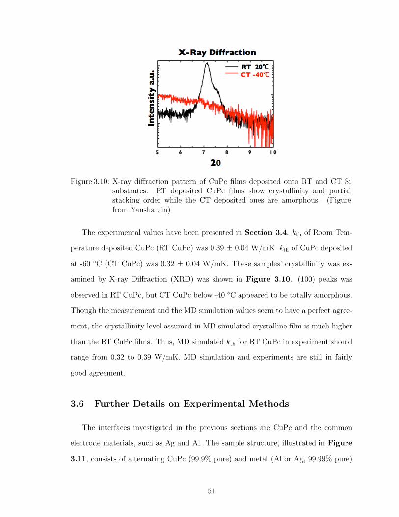
Figure 3.10: X-ray diffraction pattern of CuPc films deposited onto RT and CT Sisubstrates. RT deposited CuPc films show crystallinity and partialstacking order while the CT deposited ones are amorphous. (Figurefrom Yansha Jin)
The experimental values have been presented in Section 3.4. kth of Room Tem-
perature deposited CuPc (RT CuPc) was 0.39 ± 0.04 W/mK. kth of CuPc deposited
at -60 C (CT CuPc) was 0.32 ± 0.04 W/mK. These samples’ crystallinity was ex-
amined by X-ray Diffraction (XRD) was shown in Figure 3.10. (100) peaks was
observed in RT CuPc, but CT CuPc below -40 C appeared to be totally amorphous.
Though the measurement and the MD simulation values seem to have a perfect agree-
ment, the crystallinity level assumed in MD simulated crystalline film is much higher
than the RT CuPc films. Thus, MD simulated kth for RT CuPc in experiment should
range from 0.32 to 0.39 W/mK. MD simulation and experiments are still in fairly
good agreement.
3.6 Further Details on Experimental Methods
The interfaces investigated in the previous sections are CuPc and the common
electrode materials, such as Ag and Al. The sample structure, illustrated in Figure
3.11, consists of alternating CuPc (99.9% pure) and metal (Al or Ag, 99.99% pure)
51

layers of identical thickness, deposited by vacuum thermal evaporation at 1 A/s and
10−7 Torr onto 0.5 mm thick, [100] silicon substrates (resistivity > 10 000 Ω cm).
An electrically insulating 30 nm thick film of CuPc was deposited on top of the
multilayer stack to eliminate parasitic cross-plane leakage current (Koh et al. (2009)),
followed by a 50 µm wide wire of 40 nm nickel/400 nm silver. This top metal strip
acts as both a heater and a thermometer, with heating accomplished by applying
a low harmonic distortion current. Since the heater width is much greater than the
multilayer thickness, the measurement is primarily sensitive to cross-plane rather than
in-plane heat transfer. (Borca-Tasciuc et al. (2001))
Figure 3.11: Schematic illustration (not scaled) of the 3-ω sample on glass slides. Themultilayer CuPc/metal films request insulating capping layers to preventparasitic current. (Figure from Yansha Jin)
Recall the requirements for 3-ω method in Section 2.3 :
Firstly, kth,s kth,f , substrate thermal conductivity has to be much larger than
that of the film.
For the specific experiments in the previous section, the substrate used is Si
whose kth,s is 150 W/m−1K−1. The films’ thermal conductivity ranges from 0.2 ∼
1 W/m−1K−1, which satisfies kth,s kth,f .
Secondly, for conductive samples, an insulating layer has to be inserted to prevent
parasitic current. A 30 nm CuPc layer acts as an effective insulating layer for multi-
layer CuPc/Ag films. Proof is shown in Figure 3.12: the resistance between point
A and B in is 3.2 Ω, while between point C and D is 4.5 MΩ. The resistance values
52
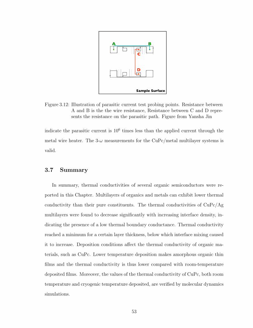
Figure 3.12: Illustration of parasitic current test probing points. Resistance betweenA and B is the the wire resistance, Resistance between C and D repre-sents the resistance on the parasitic path. Figure from Yansha Jin
indicate the parasitic current is 106 times less than the applied current through the
metal wire heater. The 3-ω measurements for the CuPc/metal multilayer systems is
valid.
3.7 Summary
In summary, thermal conductivities of several organic semiconductors were re-
ported in this Chapter. Multilayers of organics and metals can exhibit lower thermal
conductivity than their pure constituents. The thermal conductivities of CuPc/Ag
multilayers were found to decrease significantly with increasing interface density, in-
dicating the presence of a low thermal boundary conductance. Thermal conductivity
reached a minimum for a certain layer thickness, below which interface mixing caused
it to increase. Deposition conditions affect the thermal conductivity of organic ma-
terials, such as CuPc. Lower temperature deposition makes amorphous organic thin
films and the thermal conductivity is thus lower compared with room-temperature
deposited films. Moreover, the values of the thermal conductivity of CuPc, both room
temperature and cryogenic temperature deposited, are verified by molecular dynamics
simulations.
53

CHAPTER IV
Boundary Effects on Thermal and Electrical
Transport of Organic/Metal Nanocomposite
4.1 Introduction: Organic Thermoelectrics
Thermoelectric devices can be an effective in scavenging waste heat and generating
electricity, for solid-state cooling, for temperature sensing and for other applications.
Since the discovery of Bi2Te3 alloy’s thermopower in 1960s, the ZT of inorganic mate-
rials have exceeded unity. (Venkatasubramanian et al. (2001); Majumdar (2004), see
Figure 4.1). However, these materials are high cost and not environmental friendly.
Unlike Bi2Te3 and its inorganic counterparts, the synthesis of organic materials is
cheaper and less toxic, and offers other advantages, such as mechanical flexibility.
However, in terms of the ZT , organic materials are still in deficiency. One of the best
experimental demonstrations of ZT in organic semiconductors is the conducting poly-
mer PEDOT-Tos with oxidation level of 23% with a reported ZT ∼0.25.(Bubnova
et al. (2011), Leclerc and Ahmed (2011), Kwok (2012) see Figure 4.2) The bot-
tleneck for increase ZT in bulk semiconductors is the conflicting traits that favors
ZT (Section 1.3). Nanostructured materials, such as polymer nanocomposites, can
lead to enhanced thermoelectric power factors (S2σ).(Zhang et al. (2010); Kim et al.
(2010); See et al. (2010)) In these cases, the electrical conductivities of the nanos-
54

Figure 4.1: ZT ’s temperature dependence of inorganic thermoelectric materials. p-Bi2Te3 (10A)/Sb2Te3 (50A) superlattice owns the best ZT . Figure fromVenkatasubramanian et al. (2001)
tructure were increased significantly without affecting the thermopower S. Though
slightly increases in thermal conductivities were reported in some nanocomposites
(Zhang et al. (2010)), the variation in thermal conductivities of these nanostructures
were not discussed extensively, which will be addressed in this work. Inspired by the
phonon blocking and electron transmitting superlattice such as Bi2Te3 alloy, I demon-
strate the idea of using organic/metal nanocomposites with low thermal boundary
resistance between the comprising materials. The measured thermal conductivity
decreases with increasing volume fraction of the conductive fillers, while the FEM
simulation shows an ZT enhancement 10 fold around the concentration that reaches
the lowest thermal conductivity.(Jin et al. (2013)) It is anticipated that the combi-
nation of chemical modifications, power factor optimization and thermal boundary
engineering can amount the maximum ZT of organics close to 1.
55

Figure 4.2: ZT optimization of PEDOT:Tos. By controlling the oxidation level ofthe polymer, the maximum ZT = 0.25 is reached. Figure from Bubnovaet al. (2011)
4.2 Characterization of Co-Deposited Organic/Metal Films
The composites in this work were fabricated using vacuum thermal evaporation,
and CuPc and Ag were co-deposited in the vacuum chamber. I first characterized
these co-deposit films.
TEM images is shown in Figure 4.3, on samples with various of thickness, growth
rate and filler concentrations. The images prove that co-deposition of CuPc and
silver produced films of CuPc with dispersed Ag nanoparticles. The average radius
of particle of shown in Table 4.1, ranging from 1.8 nm to 2.9 nm.
xAg Thickness in nm Nanoparticle radius in nm
10% 50 1.9±0.210% 50 1.8±0.410% 150 2.2±0.820% 150 2.9±0.6
Table 4.1: Jin et al. (2013)
56

Figure 4.3: TEM images of CuPc/Ag nanocomposites with various thickness, silverconcentrations and growth rates. (a) 50 nm xAg = 10%, growth rate ∼0.1 A/s, particle radius 1.9 ± 0.2 nm; (b) 50 nm xAg = 10%, growth rate∼ 0.5 A/s, particle radius 1.8 ± 0.4 nm; (c) 150 nm xAg = 10%, growthrate ∼ 0.5 A/s, particle radius 2.2 ± 0.8 nm; (d) 150 nm xAg = 20%,growth rate ∼ 0.5 A/s, particle radius 2.9 ± 0.6 nm. Figure from Jinet al. (2013)
57

Figure 4.4: (Left) X-ray diffraction pattern of CuPc/Ag nanocomposites with differ-ent concentrations. Silver peaks (111) and (002) were observed. (Right)X-ray diffraction of single CuPc film with various of thickness. Full-WidthHalf Maximum (FWHM) is directly related to level of crystallinity. Theinset indicates the crystallinity is proportional to the thickness. Figurefrom yansha.
The X-ray diffraction patterns of these samples are shown in Figure 4.4 (Left).
Comparing to single CuPc films in Figure 4.4 (Right), the peak at 6 degree (CuPc
(100)) was not observed in the mixed films; the only peak that can be seen is the silver
(100). These suggested the short ranged order in organic matrix(CuPc) was broken
by the filler (Ag), and Ag formed smaller crystalline particles inside the matrix.
4.3 Electrical/Thermal Conductivity of Organic/Metal Nanocom-
posites
The work in this section is collaborated with Sam Nola and the experimental data
on electrical and thermal measurements was collected by her.
4.3.1 Electrical Conductivity: Percolation and Charge Trapping
Results from electrical measurement on organic-metal nanocomposite films are
presented in Figure 4.5. The electrical conductivity (σe) showed a percolation-
58

Figure 4.5: Electrical conductivity measurements on CuPc/Ag nanocomposites withvarious xAg%. Dotted line is the fitting from the percolation model. Fig-ure from Jin et al. (2013)
like behavior above xAg% = 10%, with critical fraction of silver by volume xc,e% =
20%. Also observed was an abrupt dip of σe in the ultra dilute regime (xAg ∼
5%). This is potentially due to the mismatch between organic and metal in charge
carrier mobility and in Fermi levels. The work function of silver and the nature of
metal/organic semiconductor interfaces is such that the injection barrier for holes,
which have a comparatively high mobility in CuPc, is greater than the injection
barrier for electrons, (Kahn et al. (2003); Antohe et al. (1991)) see inset of Figure
4.5. Isolated silver particles act as traps, and the barrier for re-injection would likely
decrease electrical conductivity. Similar phenomena have been reported in pentacene
films with gold nanoparticles embedded (Tseng and Tao (2009)), where the gold
nanoparticles acted as a floating gate by trapping carrier charges.
In conclusion, the electrical conductivity follows the percolation trend in general,
with abrupt dip at lower concentrations due to charge trapping.
59

Figure 4.6: Thermal conductivities of CuPc/Ag nanocomposites with various xAg%are plotted with error bars. The dashed line are the Hybrid model devel-oped by Sam Nola (Macromolecular Engineering, University of Michigan,Ann Arbor). Figure from Jin et al. (2013)
4.3.2 Thermal Conductivity of Organic/Metal Nanocomposites
Both σe and kth scale similarly with charge carrier concentration in most materials,
however, in CuPc-Ag nanocomposites, they appeared to be decoupled in the dilute
regime. No percolation threshold was observed for thermal conductivity (kth) below
xAg% = 30%. Moreover, shown in Figure 4.6, kth first decreased at low xAg%
and reached a minimum value before increasing again. Effective medium theory
considering the boundary effects had predicted similar trend for general conductivity
of composites. Torquato and Rintoul (1995) introduced a resistive interfacial media
between the two phases and rigorously modeled the composites as a 3-phase system.
The model suggested the initial drop in conductivity can only be achieved in systems
with extra low thermal boundary conductance, of which CuPc-Ag nanocomposites
happened to be an example. For thermal conductivity, a simplification of the Torquato
60

model can be written as
kth = km[1 + x(1− α + 3R)/α]−1 (4.1)
where α is the conductivity ratio between filler and matrix α = kCuPc/kAg and R =
kCuPc/rGb in which r is particle radius.
Figure 4.7 shows an illustration of 3rd phase modeling and Torquato’s results
following Eq. 4.1, it is clear that the model is only valid at the low concentration
regime. The limitation is due to the assumption from Torquato and Rintoul (1995)
that the particles are not overlapping with each other.
4.4 Finite Element Simulation on Transport Properties of
Nanocomposites
To quantitatively evaluate the thermal conductivity kth of organic/metal nano-
composite at the entire range of filler concentration, the corresponding 2D composite
structure was generated and its thermal conductivity was solved using the finite ele-
ment modeling package in COMSOL MULTIPHYSICS with MATLAB v4.2.
4.4.1 Conductivity Simulation Set-up
The simulation collection consists of a Copper Phthalocyanine (CuPc) matrix with
randomly distributed Silver (Ag) particles confined in a 2D/3D box. A 2D example
and the general principles of the simulation is shown in Figure 4.8. The Ag particles
were assumed to be round(2D)/spherical(3D) with radius r and their coordinates are
randomly generated by MATLAB. By varying the number of Ag particles N , the Ag
volume fraction xAg% could be controlled. The thermal boundary conductance was
introduced as a third phase by selecting the Thin Thermally Resistive Layer boundary
condition in COMSOL. The layer thickness δ was set to be 1 nm: the experimentally
61
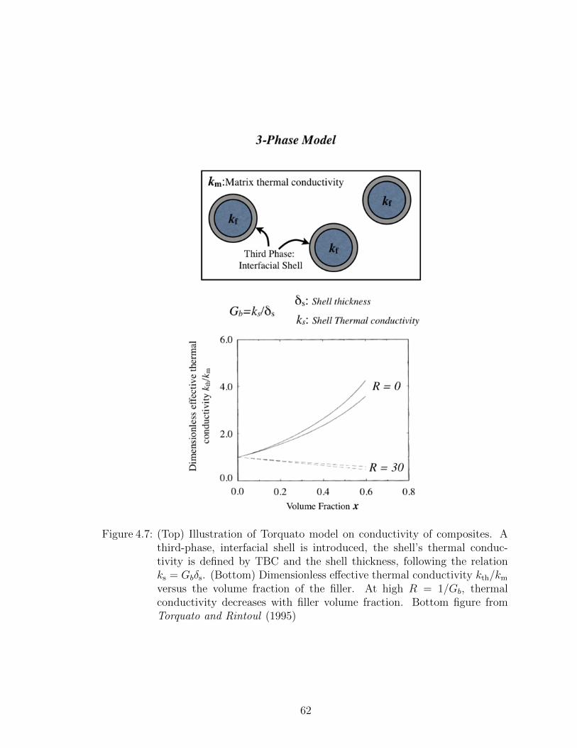
Figure 4.7: (Top) Illustration of Torquato model on conductivity of composites. Athird-phase, interfacial shell is introduced, the shell’s thermal conduc-tivity is defined by TBC and the shell thickness, following the relationks = Gbδs. (Bottom) Dimensionless effective thermal conductivity kth/km
versus the volume fraction of the filler. At high R = 1/Gb, thermalconductivity decreases with filler volume fraction. Bottom figure fromTorquato and Rintoul (1995)
62

Figure 4.8: FEM of nanocomposites’ thermal conductivity. (Top), General principleof thermal conductivity modeling: A temperature gradient of 0.2 K is setbetween the top and bottom boundaries; other sides are made to be adia-batic. Thermal conductivity equals the total normal heat flux(integratedheat flux from all nodes at the top boundary) over the temperature gra-dient. Figure from yansha.
63

measured RMS roughness of the CuPc/Ag interfaces in the composite; its thermal
conductivity k∗th was determined using equation
k∗th = δ ·Gb (4.2)
where Gb is the thermal boundary conductance of CuPc/Ag interfaces, which was
found to be 13 MW/m2K. By applying a temperature difference ∆T between the top
and bottom surfaces of the box and setting all other surfaces as adiabatic, the thermal
conductivity of the composite can be obtained by the relation Eq. 2.1, where q is
the heat flux integrated over all nodes at the top surface. ∆T is selected to be 0.2 K
and the distance between the top and bottom surfaces is chosen as 100 nm, matching
to the temperature change in 3ω measurements which ranges from 0.05 K to 0.25 K
and the thickness of the multilayer structure tested that is 80 nm to 120 nm.
4.4.2 Pseudo-3D Simulation
The simulation results used to compare with experiment are “pseudo 3D”, calcu-
lated from the 2D results following the equation:
kth,3D = kCuPc −As,3D
As,2D
(kCuPc − kth,2D) (4.3)
where As represents the surface area. With the constraints that the concentration
xAg% is identical in both 2D and 3D cases
xAg% =N3D · 4
3πa3
V=N2D · πa2
A(4.4)
the pre-factor in 4.3 can be expressed as
As,3D
As,2D
=N3D/V
N2D/A· 4πa2
2πa= 1.5 (4.5)
64

Figure 4.9: 2D and 3D FEM simulation at sam silver concentration in ultra diluteregime (xAg = 0.8%). Thermal conductivity value from FEM for 2D and3D agree well with the “pseudo 3-D” extrapolation, Eq. 4.5. FigurefromJin et al. (2013).
The reason for doing “pseudo 3D” other than real 3D is the the complexity of geometry
grows tremendously from 2D to 3D under same silver volume concentrations. The
more than ten thousand of pieces are needed to be united and defined as resistive
boundaries which increase the manual setting-time and calculation time.
The “pseudo 3D” kth is within 10% margin of error compared to real 3D FEM
simulation at low concentrations, proved by low concentration “real” 3D FEM simula-
tions. FEM simulation set-up is illustrated in Figure 4.9. The 2D simulation output
of COMSOL is shown in Figure 4.9 (a), with randomized particle coordinate within
the 2D simulation box. In Figure 4.9 (b). The 2D and 3D simulation shares a same
silver volume fraction at ultra dilute regime xAg% = 0.8%, the thermal conductivity
is simulated to be kth,2D = 0.3789 W/mK. Following Eq. 4.3, kth,3D = 0.3734 W/mK,
the pre-factor A3D/As,2D is 1.43, within 5% error compared with our calculated value.
The degree of accuracy in the “pseudo” 3D calculations enabled us to use the ap-
proximation to compare with experimental data and conduct multi-parameter anal-
ysis in the following sections.
65

Figure 4.10: The particle size effect on kth of CuPc/Ag nanocomposites. FEM resultsfor composites with radius of 2 nm, 3nm, 4 nm and 5 nm. The inter-facial area increases with the smaller particle sizes at the same xAg%,thus the thermal conductivity drops with the decreasing particle size.The percolation threshold for the corresponding particle sizes are listed,which increases with the particle sizes. Figure from Jin et al. (2013)
4.4.3 Tunable parameter I: Particle Size
Curves of thermal conductivity of the CuPc-Ag nanocomposites with different par-
ticle radii were plotted against xAg%. Percolation threshold increases with the silver
particle radius as listed in Figure 4.10. Statistically it is easier for smaller particles
to form percolation path at the same filler volume fraction. Before the percolation
threshold, however, a reduction of kth is observed at lower concentrations (Figure
4.10). This trend is attribute to the boundary effect: under the same silver concen-
trations, the interfacial area also changes with silver particle size. This reasoning is
similar to our discussion for the difference between 2D and 3D.
This strong influence of particle size on nanocomposites’ thermal conductivity re-
66

quest us to use the accurate particle radii comparing to the experiment. In terms of
tuning thermoelectric properties, the particle radius is one of the tunable parameters.
For particles smaller than 1 nm diameter, which is the phonon mean free path of CuPc
matrix, quantum effects and ballistic transport might interfere with the continue de-
creasing trend of kth with the particle radius. However, for CuPc-Ag nanocomposites,
the particle radius larger than 4 nm diameter and our current results hold.
4.4.4 Tunable parameter II: Thermal Boundary Conductance
Another tunable parameter for the thermoelectric properties in nanocomposites
are the thermal boundary conductance Gb. Thermal conductivity is calculated with
different Gb at a fixed particle radius. The particle radius is set at 5 nm for the thermal
conductivity plots Figure 4.11. kth is found to be increasing monotonically with
xAg% without the boundary effect, which is presented by the perfect(∞) interfacial
conductance. As the interfacial conductance decreases, kth starts to drop at first
then rises up at higher concentrations, which matches the experimental trend of kth
discussed in Section 4.3.2, which proved adding the thermal boundary conductance
is the reason for the drop of kth.
In addition of supporting the boundary effect on thermal conductivity of com-
posites, the simulation results also suggesting another interesting fact: the xAg% for
the minimum kth also changes with Gb. As shown in Figure 4.11 and replotted in
the inset Figure 4.11, the lower the thermal boundary conductance, the higher the
xAg%(min). This piece of information on where kth the minimizes is very important
in optimizing thermoelectric efficiency.
4.4.5 Proof of Validity of the FEM simulation
Recall that the advantages of FEM simulation over the analytical Torquato model
is that FEM can predict in the entire range of silver concentrations and the “pseudo
67

Figure 4.11: Boundary effect on kth of CuPc/Ag nanocomposites. FEM results forcomposites with various values of thermal boundary conductance (Gb).Smaller Gb yields to smaller kth. The xAg% that reaches the minimumthermal conductivity also changes Gb. The inset shows this critical con-centration for each TBC values. Figure fromJin et al. (2013)
68

Figure 4.12: Thermal conductivity measurements on nanocomposites with variousfiller concentrations are plotted with error bars. Red dashed line iscalculated by Hybrid model (Sam Nola). Black dotted lines are FEMresults corresponded to 2 nm and 3 nm Ag particle radii, respectively.Figure adapted from Jin et al. (2013).
3D” results extracted from 2D simulation is enough accurate to compare to the mea-
surements. The simulations adopted the measured particle radius 2 nm to 3 nm (in
Table 4.1) and the measured TBC in Table 3.2 for CuPc/Ag nanocomposites in
order to seek better agreement with the experiment.
Thermal conductivities calculated from FEM simulations with 2 nm and 3 nm
radius are plotted in Figure 4.12 along with the experimental value. As can be seen,
most of the measured data points lie within the range of the 2 nm and 3 nm simulation
curves. Note the hybrid model presented in the Figure 4.12 was developed by Sam
Nola, combining some of the existing models, the hybrid model is discussed in Jin
et al. (2013).
The agreement between experiment and modeling data strongly proves the va-
lidity of the FEM simulations and further in this chapter, a novel way to optimize
69

thermoelectric efficiency for organic/inorganic hybrids is presented based on the FEM
simulations.
4.4.6 TE Figure of Merit Enhancement
The thermoelectric Figure of merit (ZT ) (Eq. 1.31) can represent the efficiency of
TE devices, and lowering thermal conductivity, enhancing electrical conduction can
optimize ZT .
Electrical conductivities are modeled in the same set of structures, while electrical
and thermal conduction can be decoupled in composites, if electrical conduction is not
hindered by the boundary phase, and particularly if σe increases with filler concen-
tration, as shown in Figure 4.13. The Seebeck coefficient values are approximated
from the simulated σe following the linear relationship between S and ln(σe)(Kim
et al. (2011); Yu et al. (2011)) in moderately doped organic semiconductor system,
plotted in Figure 4.13.
S = −kBq
lnσe + C1 (4.6)
where C1 is related to carrier mobility and density of states and we assume to be a
constant in our study.
A multi-parameter contour plot of ZT versus particle radius, r, and filler con-
centration, xf% is shown in Figure 4.14, based on the well-characterized system of
CuPc - silver nanocomposites (Jin et al. (2011, 2012)). TBC is a constant in the plot,
which is 13 MW/m2K – the Gb for CuPc-Ag interfaces. The contours are normalized
to the ZT of CuPc, and a maximum ZT enhancement factor of 5 is achieved relative
to bulk CuPc. Another finding that can guide the design of TE materials is the op-
timized filler concentration for filler particles of different sizes. The optimized filler
concentration ranges from 20% to 30% as the filler particle size grows.
With the optimized percentages extrapolated from a set of contour plots with
different Gb, the maximum enhancement is calculated using two parameters: Thermal
70

Figure 4.13: FEM calculated electrical conductivity and the Seebeck coefficient ex-tracted from the linear relation between S and ln(σe)Jin et al. (2013)
boundary conductanceGb (ranges from 10 to 30 MW/m2K), and the radius of the filler
particles r, (ranging from 2 to 6 nm), shown in Figure 4.15. Previous work showed
that Gb at organic-metal interface originates from phonon-phonon scattering, due to
the fact that electron-phonon contribution to the boundary resistance is negligible
compared to phonon-phonon scattering (Majumdar and Reddy (2004)). In weakly-
bonded organic-inorganic hybrids(Jin et al. (2012)), TBC is mainly affected by the
interfacial bonding strength. There are also reports suggesting that the interfacial
bonding strength could be adjusted by surface modifications, like changing the side
group of a self-assembled monolayer coating (Losego et al. (2012)). Further decrease
in filler particle radius might introduce complications, such as quantum confinement
and ballistic transport. Even with these concerns, the simulation is reliable down to
r = 2 nm, because the filler particle size is still larger than the phonon mean free path
of most organic materials.(Huang et al. (2007); Sun et al. (2013)) The temperature
gradient within the higher conducting filler particle is minor influence.
71

Figure 4.14: Multi-parameter optimization of ZT of CuPc-Ag nanocomposites (Gb =13 MW/m2K). The volume fraction of the filler ranges from 0 % to 50% and particle radii from 2 to 6 nm. The optimum xAg% for differentparticle radii is indicated as the dashed black line. The enhancement ofZT is as large as 5 times. Figure from Jin et al. (2013).
72
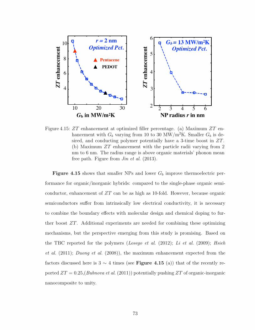
Figure 4.15: ZT enhancement at optimized filler percentage. (a) Maximum ZT en-hancement with Gb varying from 10 to 30 MW/m2K. Smaller Gb is de-sired, and conducting polymer potentially have a 3-time boost in ZT .(b) Maximum ZT enhancement with the particle radii varying from 2nm to 6 nm. The radius range is above organic materials’ phonon meanfree path. Figure from Jin et al. (2013).
Figure 4.15 shows that smaller NPs and lower Gb improve thermoelectric per-
formance for organic/inorganic hybrids: compared to the single-phase organic semi-
conductor, enhancement of ZT can be as high as 10-fold. However, because organic
semiconductors suffer from intrinsically low electrical conductivity, it is necessary
to combine the boundary effects with molecular design and chemical doping to fur-
ther boost ZT . Additional experiments are needed for combining these optimizing
mechanisms, but the perspective emerging from this study is promising. Based on
the TBC reported for the polymers (Losego et al. (2012); Li et al. (2009); Hsieh
et al. (2011); Duong et al. (2008)), the maximum enhancement expected from the
factors discussed here is 3 ∼ 4 times (see Figure 4.15 (a)) that of the recently re-
ported ZT = 0.25,(Bubnova et al. (2011)) potentially pushing ZT of organic-inorganic
nanocomposite to unity.
73

4.5 Potential Optimization of ZT for Organic Semiconduc-
tors
The FEM simulation suggested that smaller NPs and lower thermal boundary
conductance Gb is needed to achieve better a thermoelectric performance for or-
ganic/inorganic hybrids. Enhancement compared to the pure organic semiconductor
can reach as high as 10 times. However, organic semiconductor intrinsically suffers
from low electrical conductivity, it is necessary to combine the molecule structure
modifications and the boundary effects to achieve greater boost in ZT .
Discussed in Bubnova et al. (2011), the replacing of the PSS in poly(3,4-ethylenedioxythiophene)
poly(styrenesulfonate) (PEDOT:PSS) by small anions, for example Tos, increases σe
for several orders of magnitude but the Seebeck coefficient remains competitive. Ad-
ditional experiments are needed for compiling this mechanism with boundary effects
from the fillers, but the perspective is promising: for the conductive polymers like
PEDOT, the lowest Gb reported are around 20 MW/m2K. Thus, the maximum en-
hancement is 3× the current reported ZT = 0.25 which makes the ZT of organic
close to unity.
4.6 Summary
In organic semiconductors the Wiedemann-Franz law is often violated, potentially
enabling independent control over electrical and thermal conductivity, as observed
here with the organic-metal nanocomposites. This effect is attributed to the inter-
face between metal particles and organic matrix materials impeding thermal trans-
port. Thermal conductivity (kth) can be decoupled from electrical conductivity (σe)
in the composite of an archetypal organic semiconductor (Copper Phthalocyanine,
CuPc) and silver, with thermal boundary conductance as low as 13 MW/m2K at
the interface. We show that kth decreases with volume fraction occupied by silver
74

nanoparticles (xAg%) in the dilute limit, reaching a minimum value concentration,
xAg%(min)= 18%, while σe exceeds that of the pure organic semiconductor. Further
modeling indicates that ZT values of organic-inorganic nanocomposites can be po-
tentially enhanced 10 fold around xf%(min), compared to ZT of the pure compounds.
These findings suggest a novel pathway for the future design of organic thermoelectric
materials.
Introducing conductive filler particles into an organic matrix can achieve the goal
of ZT > 1 by virtue of boundary effects, which were quantitatively measured (Jin
et al. (2012)). A novel design principle emerges for tuning the overall TE behavior
of nanocomposites, demonstrated in simulations and validated by experiments for
composites comprising copper phthalocyanine (CuPc) and silver (Ag) nanoparticles.
The resistive nature of the thermal boundary between CuPc and Ag results in a kth
decrease by as much as 50%. Once the Seebeck coefficient is calculated from the
simulated electrical conductivity, and ZT ’s dependence on thermal boundary con-
ductance, effects of particle radii and filler volume concentrations can be examined.
With the interfacial engineering and particle size control, ZT enhancement by more
than a factor of 10 for organic TE materials can potentially be realized. Such a large
boost in performance calls for a nanocomposite system with low thermal boundary
conductance and small particle radii. With a combination of chemical doping, surface
treatment and thermal boundary effects, ZT > 1 is achievable for organic semicon-
ductors.
75

CHAPTER V
Origins of TBC: Interfacial Bonding
5.1 Introduction
This chapter and Ch. VI discuss the fundamental physics of thermal boundary
conductance (TBC), focusing on interfaces involving disordered organics. Interfacial
bonding strength is proposed and proved to be a crucial factor for TBC at van der
Waals bonded interfaces in this chapter. For the specific material system, CuPc/Al,
TBC is shown to be influenced by spatial non-uniformity and anharmonic phonon
transmission which are both presented in Ch. VI.
TBC values between copper phthalocyanine (CuPc) and several metals (aluminum,
gold, magnesium, silver) have been measured using the 3-ω method in Ch. III. In
conventional theories, TBC is supposed to be related to the acoustic properties of
the solid state materials. Acoustic Mismatch Model (AMM) and Diffuse Mismatch
Model (DMM) have been proposed to model the phonon transmission (Swartz and
Pohl (1989)). This section starts with the discussion of these two mismatch models,
followed by the discrepancies between the experimental and their modeling results.
Several possible factors aide from the mismatch that may influence the TBC are
discussed, and the interfacial bonding strength is the one that will be extensively
discussed in the following sections.
76

5.1.1 Mismatch Models for TBC
Mismatch models consider only the mismatch the intrinsic thermal properties of
the two materials comprising the interface. TBC is written as, Gb = q/∆T in Eq
3.1, and the heat flux q can be generally expressed by
q =
T2∫T1
Dp(ω)fp(ω)vp(ω)τpdω (5.1)
where T1 and T2 are the temperature at each side of the interface, Dp is the phonon
density of states, vp is the phonon velocity: both Dp and vp have been discussed in
Subsection 1.1.2. fp is Bose-Einstein distribution which is a function of T .
The most difficult task is the determination of τp in Eq 5.1, the transmission
coefficient. AMM and DMM have different approaches in calculating this crucial
coefficient.
Acoustic Mismatch Model (AMM): AMM assumes a perfect flatness of the
interface where phonons scatter specularly. The model shares the fundamentals with
the optics: the transmission coefficient has similar form with the Fresnel Law. Under
the assumption of normal incidence, τp,AMM yields,
τp,AMM = 4Z1Z2
(Z1 + Z2)2(5.2)
Z in Eq 5.2 is Acoustic Impedance, the product of material density ρ and sound
velocity vp (Eq 1.9), Z = ρvp. The subindexes represent the two material comprising
the interface, respectively.
Diffuse Mismatch Model (DMM): DMM on the other hand, assumes the
interface is rough compared to the dominant phonon wavelength. All phonons lost
their memory after hitting the interface and scatter in all direction diffusively. The
77

Figure 5.1: Acoustic Mismatch Model (Left) -The calculation of transmission coeffi-cient in AMM is an analogy to optical transmission, the main assumptionis coherent transport through the interface. Diffuse Mismatch Model(Right) - The transmission coefficient in DMM is related to the over-lapping of materials’ phonon DOS; Debye model, sine model and latticedynamics simulation can be used to calculated phonon DOS. (Figure byYansha Jin)
transmission coefficient in DMM is expressed as:
τp,DMM =
∑mode Dp,2fp,2vp,2∑
modeDp,1fp,1vp,1 +∑
mode Dp,2fp,2vp,2(5.3)
This transmission coefficient relates to the phonon DOS of both materials and the
overlapping between the two. For simplicity, most of work use the Debye model (Eq
1.12) as phonon DOS.
The principles of AMM and DMM are shown in Figure 5.1, both have their
limitations and advantages. However, for organic/metal multilayer as deposited under
RT by VTE, diffuse scattering is a more reasonable assumption (Hopkins (2009)).
The nature of the scattering, whether specular or diffuse, is decided by the thermal
coherence length Lcoh and the RMS roughness of the interfaces, δrms. An quantified
parameter is defined to represent the nature of scattering, the degree of specularity,
psp
psp = exp
[− 16π2δ2
rms
L2coh
](5.4)
In case of the CuPc/Ag multilayers measured in Chap III, the roughness of the
78

interfaces δrms is around 1∼2 nm. The coherent phonon length, Lcoh = hvp/kBT ,
where vp is the sound velocity of CuPc. Measurements in Sun et al. (2013) suggest
vp for CuPc is 3000 m/s. Thus, Lcoh ∼ 5 A. Obviously, the coherent phonon length
is nearly 5 times less than the RMS roughness, that leads to psp ∼ 0. Degree of
specularity close to zero suggests a diffuse scattering at CuPc/Ag interface.
Figure 5.2: TBC vs Debye temperature ratio. Debye model is often used as an ap-proximation for phonon DOS. If DMM is valid, TBC should correlateto the Debye temperature ratio. TBC values shown here roughly followthe monotonic increasing trend, but some data points including TBC ofCuPc/metal interfaces do not follow this general trend. (Figure fromStevens et al. (2005) and adapted from Jin et al. (2012))
5.1.2 Failure of Mismatch Models
However, DMM also cannot accurately predict the TBC values of material systems
such as CuPc-metal, and the discrepancies also exist in other material systems. In
Stevens et al. (2005), a collective set of TBC values is shown in Figure 5.2, plotted
versus the Debye temperature ratio. Generally, Debye model is a good estimation to
79

the phonon DOS, thus the Debye temperature ratio roughly correlates to the TBC
values. Roughly, the TBC monotonically increases with this ratio. However, quite a
few data points deviate from the monotonically trend, this discrepancy is more severe
in for the CuPc-metal interfaces.
Figure 5.3: TBC of CuPc/metal interfaces calculated by AMM, DMM and measuredby 3-ω. The values predicted by AMM and DMM are five times than themeasured values. (Figure from Jin et al. (2012))
While both AMM and DMM predict that CuPc/gold interface has the lowest
transmission probability and TBC among the four CuPc/metal interfaces measured
here, see Figure 3.5, the experimental results indicate otherwise: TBC of CuPc/Ag
is lowest (1.3 ± 0.3 × 10⁷W/m2K) and CuPc/Al has the largest interface thermal
conductance (5.0 ± 1.5 × 10⁷W/m2K). (See Table 3.2). If one considers only the
materials’ intrinsic vibrational properties (AMM and DMM), the observed trends in
TBC cannot be explained and the predicted values are approximately 5 to 50 times
larger than that measured by experiment. (See Figure 5.3, Jin et al. (2012))
80

Figure 5.4: TBC changes with the oxidation level of the interfaces. Experimentallymeasured TBC values w/ and w/o BOE treatment are plotted with errorbars. Dashed black line corresponds to DMM, and colored lines are themodeling results from Hopkins et al. (2010). (Figure from Hopkins et al.(2010))
5.1.3 Other Contributing Factors to TBC
Many theories have been proposed to explain the discrepancies between the various
mismatch models and the experiments. The interfacial disorder and the size effect
have been proved to be part of the reason. Oxide layer was introduced to change the
chemistry and the morphology at the interface in Hopkins et al. (2010). Gb increases
after the Buffered Oxide Etch (BOE) treatment (See Figure 5.4). The size effect
is presented in Li and Yang (2012), shown in Figure 5.5, the phonon confinement
results in new peaks/dips in the phonon transmission.
Among the possible factors that are contributing to the TBC, the interfacial bond-
ing strength is the most important factor for systems involving organics, because the
organic materials are weakly bonded by van der Waals interaction. Another reason
81

Figure 5.5: Phonon transmission peaks/dips change due to the size effect. Phonontransmission is calculated using the Green Function Method in Si withdifferent transverse confined sizes. (Figure from Li and Yang (2012))
for the research attention to interfacial bonding is that its correlation to TBC only
existed in theory before the year 2010. One example of the theoretic modeling is Ong
and Pop (2010), see Figure 5.6: As interfacial bonding strengthened in molecular
dynamics simulation, the temperature discontinuity ∆T became small indicating a
larger TBC.
5.2 Correlation Between Interfacial Bonding vs TBC at Or-
ganic/Metal Interfaces
In this section, a definite relation between interfacial bonding strength, which is
qualified by peel-off tests, and TBC at CuPc/metal interfaces experimentally.
82

Figure 5.6: MDS of TBC’s dependence on the interfacial bonding for CNT/Au in-terfaces. (a) The decay of the normalized CNT temperature varies withthe CNT/Au substrate interaction strength χ. (b) Natural logarithm of(a). (c) Cross-sectional view of (10, 10) CNT for different χ values: CNTdeforms more when χ becomes larger. (Figure from Ong and Pop (2010))
5.2.1 Peel-off Test
Briefly, several Indium Tin Oxide (ITO) substrates were vacuum-coated with 100
nm thick CuPc films simultaneously. The samples were then masked and different
metals were vacuum evaporated through arrays of 1 mm apertures in the masks,
capped by silver to prevent corrosion in the ambient and ensure identical adhesion
to the scotch tape. After the test, the samples were imaged using optical microscopy
and SEM. A similar approach to characterizing interfacial adhesion strength was
introduced by Losego et al. (2012): by varying the laser fluency, the induced stress
load is modified, and failure of the interface resulting in delamination was observed
at different stress amplitudes for different material systems.
The schematic drawing of the peel-off test is present in Figure 5.7 along with a
83

Figure 5.7: (Top) - Schematic representation of the peel-off test. (Bottom) - Opticalmicrographs of the deposited structure (rolling direction indicated) alongwith images of 1 mm -diameter dot before and after peel off. (Figure fromJin et al. (2012))
plane view of the films along with optical micrographs of the 1 mm diameter dot be-
fore and after the peel-off (CuPc-Ag interface). Peel-off percentage was defined as the
statistical average over 10 or more dots as the ratio of the area of the layered struc-
ture (Ag/metal/CuPc/ITO) that breaks at the metal/CuPc interfaces to the total
area covered by metal. The peel-off percentage can indirectly quantify the bonding
strength by comparing the interfacial bonding of CuPc/metal with CuPc/ITO and
bonding of CuPc to itself. Interface bonding of CuPc/ITO is observed via peel-off
tests to be approximately of the same strength as CuPc interior bonding.
5.2.2 Experimental Confirmation
The peel-off test can semi-quantitatively describes the interfacial bonding strength,
and a definite correlation between these bonding strength and TBC is shown: as we
plot the TBC against the peel-off percentage, the trend clearly indicates that the
weaker the interfacial bonding (which is represented by larger peel-off percentage),
84

Figure 5.8: Experimental proof of the correlation between TBC and interfacial bond-ing strength. (Top) - Representative SEM images of the stacks afterpeel-off. Metal was deposited on CuPc film using masks with dots of 1mm diameter arrays. (Bottom) - TBC of CuPc-metal interfaces versuspeel-off percentage. Peel-off percentage is the ratio of the area of thelayered structure (Ag/metal/CuPc/ITO) that breaks at the metal/CuPcinterfaces to the total area covered by metals. (Figure from Jin et al.(2012))
the smaller the TBC of the corresponding CuPc/metal system. (See Figure 5.8 -
bottom) SEM images are arranged from left to right starting from the interface with
the highest peel-off percentage to the lowest in Figure 5.8 -top.
To further confirm the precise location in the stack where delamination occurs dur-
85

Figure 5.9: X-ray photoelectron spectroscopy evidences on peel-off tests. (a) Beforethe peel-off test. Ag, Cu, C, N,O peaks were observed, indicating thatAg and CuPc are at the surface of the film. (b) After the peel-off test.the C, N, Cu, O, Indium peaks suggest that Indium tin oxide and CuPcare on the top surface. (Figure by Yansha Jin)
ing peel-off, we have performed X-ray Photoelectron Spectroscopy (XPS) on CuPc/Au
sample before and after peel-off as an additional test. The results have confirmed that
the bright region is indeed the ITO substrate devoid of any organic or metal films
(See Figure 5.9). Thus, the significant contribution of the interfacial bonding ef-
fect to TBC is experimentally confirmed for this type of van der Waals interfaces.
Noted that the interfacial bonding effect overrides the trend of the materials thermo-
property mismatch, represented by the Z ratios in Figure 5.8, which leads to the
next question: How to evaluate the balance of the contributions from two major con-
tributors to TBC at van der Waals bonded interfaces, the thermo-property mismatch
and the interfacial bonding.
5.3 TBC Modeling with Bonding Modifications
Further understanding of the above question can be provided the TBC model-
ing and simulations. A short review of previous models/simulations that consider
both material property and interfacial bonding are discussed in this section. Both
86
analytical modelings and computer simulations showed proofs of interfacial bonding
involvements: Prasher (2009) proposed a model that incorporates the weak nature
of van der Waals bonding into the traditional acoustic mismatch model, relating the
bond strength to TBC. More recently, Zhang et al. (2011) presented the scattering
boundary model in atomic junctions to investigate the significance of bonding. The
model indicates that the cut-off frequency and the TBC are linearly dependent with
the interface bonding strength in 1D chains. In terms of computer simulations, using
lattice dynamics, Stoner and Maris (1993) and Young and Maris (1989) showed that
the phonon transmission coefficient is strongly affected by the spring constant linking
the two materials. Molecular dynamics simulation work from Ong and Pop (2010),
mentioned earlier in Section 5.1.3, predicted a linear dependence of the TBC on the
strength of the interface interaction for weakly bonded carbon nanotubes and SiO2.
These works above are summarized in the following subsections.
5.3.1 Modified Acoustic Mismatch Model
Prasher (2009) presented a model that incorporates the weak van der Waals
bonding into the traditional acoustic mismatch model, relating the interfacial bond
strength to TBC. The model is based on the harmonic approximation that the two
materials are connected by a spring. The transmission coefficient under this condition
is written as
τp,Prasher =4Z1Z2
(Z1 + Z2)2 + ω2
n2K2sp
(Z1Z2)2(5.5)
where n is the number density of the interfacial atoms and Ksp is the spring constant.
The spring constant can be obtained by the second derivative of the interacting po-
tential, φ(r). Take Lenard Jones (LJ) potential for example,
φ(r) = −4ε
[(σLJr
)6
−(σLJr
)12](5.6)
87

where σLJ is the length scale parameter for LJ potential. The spring constant Ksp
yields,
Ksp =
(∂2φ
∂r2
)r=r0
=72ε
21/3σ2LJ
(5.7)
I replot the transmission coefficient’s dependence on the acoustic impedance ratio
Figure 5.10: Transmission coefficient modeled following the work,Prasher (2009),with acoustic impedance ratio Z2/Z1 as 1 and 5. (Figure by YanshaJin)
and the spring constant in Figure 5.10. Comparing the two curves under Z2/Z1 = 1
and Z1/Z2 = 5 conditions, while the range of Ksp is kept the same, τp,Prasher continues
varying at high spring constant regime in the Z1/Z2 = 5 while τp,Prasher of the Z1/Z2 =
1 is already saturated.
Prasher’s model is modified from acoustic mismatch model, thus not rigorous
in describing rough interfaces. Another limitation for this model is the assumption
of the harmonic spring connecting the two materials, which exclude the multiple
phonon transmission. Multiple phonon (anharmonic) transmission is important at
high temperature (T TDebye), and this effect will be discussed extensively in Ch.
VI.
88

5.3.2 Scattering Boundary Model
Zhang et al. (2011) reported the Scattering Boundary Model with interfacial bond-
ing modification based on an atomic junction. The schematic representation of a 1D
atomic junction is shown in Figure 5.11. The mathematical derivation is similar
with 1-D monatomic chain (Eq 1.14).
Figure 5.11: Schematic illustration of the two-junction atomic chain in the ScatteringBoundary Model. The right and left regimes are semi-infinite represent-ing the two materials. The middle part is the interfacial regime whichis coupled by harmonic springs to each sides, with spring constants rep-resented by k12 and k23. The mass and spring constants are defined asindicated. (Figure from Zhang et al. (2011))
The main idea of the model is the introduction of a few atoms of intermediate
chain, with its own mass and spring constants, creating a two-junction atomic chain.
(See Figure 5.11). Solution of the equation of motion yields to the expression for
transmission coefficient as follows,
τp,SB =(1− |r12|2)(1− |r23|2)
|1− r23r21λ22(Nc − 1)|2
(5.8)
where rij is
rij =ki(λi − 1/λi)(kj − kij − kj/λj)
(ki − kij − ki/λj)(kj − kij − kj/λj)− k2ij
− 1 (5.9)
where λj = eiqjaj , qj is the wave vector, aj represents the interatomic spacing for the
atom at jth atomic site.
The major result for this model is that a maximum transmission happens at
89

Figure 5.12: TBC dependence on interfacial spring constant (k12) calculated by one-junction atomic junction, Scattering Boundary Model, with k12 as thepoint-junction spring constant. k1 = 1.0 and m1 = 1.0. (Figure fromZhang et al. (2011))
k12 = 2k1k2k1+k2
for a single junction. This value is the geometric average of the bulk
spring constants of the two materials. As a result, an asymptote is observed in TBC
at this interfacial spring constant value (See Figure 5.12).
Scattering Boundary Model is more fundamental in physics than the Prasher’s
model, but has difficulties defining the mass and spring constant in complicated 3-
D complex with non-trivial molecular structure, such as CuPc and other organic
molecules.
To sum up Subsection 5.3.1 and Subsection 5.3.2, theories like Prasher (2009)
ascribe the interfacial bonding dependence to the low-pass filter effect: the harmonic
interfacial spring only supportes vibrational modes with frequencies smaller than the
cut-off frequency ωc, which is proportional to the interfacial bonding strength rep-
resented by the interfacial spring constant Ksp; When the bonding is strong enough
(and ωc large enough), nearly all the existing modes are supported and TBC is max-
90
imized at a saturation value, Gb0. Other works likeZhang et al. (2011) suggest the
TBC is maximized at the harmonic average of the two spring constants of the leads,
and decrease, asymptoting to a constant Gb0.
Due to the various of limitations of the analytical models, some computational
efforts come in aiming for a more complete understanding on TBC. The following
subsections present Lattice Dynamics Simulations (LDS) and Molecular Dynamics
Simulations (MDS), while still focusing interfacial bonding strength and TBC rela-
tions.
5.3.3 Lattice Dynamics Simulations
Stoner and Maris (1993) and Young and Maris (1989) are among the earliest the-
oretical works relating the interfacial spring constant to phonon transmission. The
frameworks of lattice dynamics has been described in Subsection 1.1.2. The phys-
ical picture is similar to Scattering Boundary Model, Subsection 5.3.2, with single
junction connecting by a tunable harmonic spring.
Related results from these works are shown in Figure 5.13. The average phonon
transmission coefficient is plotted against the transmission frequency; while the in-
terfacial springs strength varies in this series of plots. For small Ksp (less than effec-
tive spring constants of the materials), the transmission coefficient decreases because
the weak bonding strength cannot support transmission at higher frequencies. As
Ksp increases, transmission at higher frequencies increases, suggesting the ability of
the connecting spring’s in supporting the phonon modes at these higher frequencies.
These results share the similarity with the low-pass filter effect as Prasher (2009). At
the same time, further increase of Ksp reduces the transmission. In Young and Maris
(1989), this effect is well-explained by considering the extreme condition, Ksp →∞,
which makes the interface a completely rigid entity with the interfacial particle mass
the sum of the two comprising materials’ atomic masses. This produces a heavier
91

Figure 5.13: Average phonon transmission coefficient versus frequency with variousof interface spring constants values. Material 1: k=1, m=1; Material 2:k=4, m=1. For weak interface springs, high frequency phonon modes arenot supported. If the springs strengthen further, all phonon modes canbe supported; Phonon transmission drops slightly after an asymptotepoint. (Figure from Young and Maris (1989))
interface junction, which explains the transmission reduction at high Ksp.
5.3.4 Molecular Dynamics Simulations
In recent years, Molecular Dynamics Simulations (MDS) has emerged as a pow-
erful tool for calculating of thermal properties including those of organic materials
(Hu et al. (2009), Hu et al. (2010), Ong and Pop (2010)). Besides Ong’s work that
mentioned in the Subsection 5.1.3, Hu et al. (2010) also discussed MDS results on
Au/Si interface by inserting Self-Assembled Monolayers (SAM) in between, shown in
Figure 5.14. The tuning of the interfacial bonding strength was achieved by varying
the SAM-Si interaction in the MD simulations. Increasing the Si-SAM interaction to
five times of the original value significantly decreased the temperature discontinuity
92

at the Si-SAM interface, which indicated a smaller TBC.
Figure 5.14: (Top) Side-view of the simulation collection, Au-SAM-Si. (Middle) Equi-librium temperature profile for a standard Au-SAM-Si junction. (Bot-tom) - Equilibrium temperature profile for the same junction, with five-time stronger Si-SAM interaction. (Figure from Hu et al. (2010))
MDS on systems involving complicated molecules like CuPc, however, has seldom
been reported. While more extensive details regarding the MDS of the CuPc/metal
systems will be provided in Chen Shao’s publications and thesis (Kieffer group, Uni-
versity of Michigan, Ann Arbor, Materials Science and Engineering), the following
section briefly describes how the interfacial bonding strength is tuned, along with its
relationship to the Young’s modulus relevant to the discussion.
93

5.4 Molecular Dynamics Simulations on CuPc-Metal Junc-
tions
A Lennard-Jones 9-6 potential, UvdW is employed to describe the interface and to
represent the strength of interfacial interactions.
UvdW =∑i,j
χεij
[2
(r 0ij
rij
)9
− 3
(r 0ij
rij
)6](5.10)
where rij is the distance between atoms; εij is defined as the square root of the product
of the energy parameter of the materials at each side of the interface.
εij =√εiεj (5.11)
The geometric mean is a good approximation for the interface energy parameter when
systems do not involve highly polar molecules.
Figure 5.15: Work of adhesion scales linearly with the bond ratio (a) CuPc/Au, (b)CuPc/Ag and (c) CuPc/Al. (Figure from Jin et al. (2012))
The interfacial bonding strength could be further tuned by the bond ratio χ
in Eq 5.10. To confirm this, the work of adhesion at the interface is calculated.
The sandwiched CuPc/metal junction is first relaxed under room temperature with
94
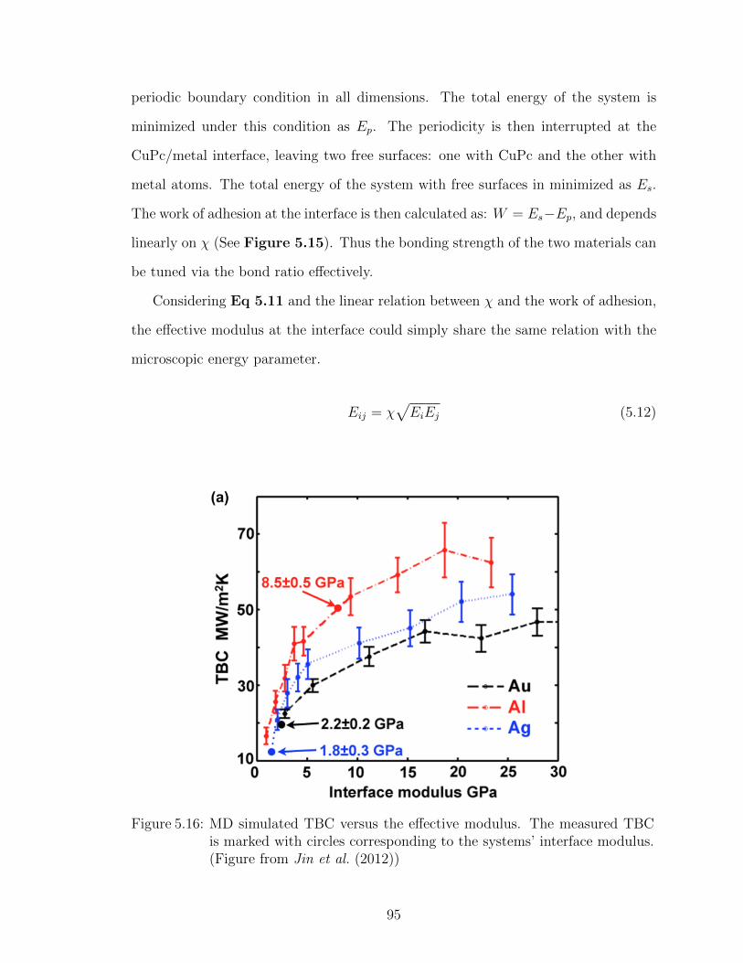
periodic boundary condition in all dimensions. The total energy of the system is
minimized under this condition as Ep. The periodicity is then interrupted at the
CuPc/metal interface, leaving two free surfaces: one with CuPc and the other with
metal atoms. The total energy of the system with free surfaces in minimized as Es.
The work of adhesion at the interface is then calculated as: W = Es−Ep, and depends
linearly on χ (See Figure 5.15). Thus the bonding strength of the two materials can
be tuned via the bond ratio effectively.
Considering Eq 5.11 and the linear relation between χ and the work of adhesion,
the effective modulus at the interface could simply share the same relation with the
microscopic energy parameter.
Eij = χ√EiEj (5.12)
Figure 5.16: MD simulated TBC versus the effective modulus. The measured TBCis marked with circles corresponding to the systems’ interface modulus.(Figure from Jin et al. (2012))
95

Figure 5.16 presents the MD simulated TBC versus the effective modulus for
CuPc/Ag, CuPc/Au and CuPc/Al. Though the MD simulated results cannot explic-
itly exclude the asymptoting behavior nor the monotonic increase trend, it supports
the low-pass filter theory and considers two and multiple phonon transmission pro-
cesses.
The next section presents the comprehensive analysis of MD simulation on TBC,
TBC measurement data and the peel-off test results, focusing on the consistency of
these results.
Figure 5.17: Experimentally measured TBC values of different materials system madeby VTE plotted versus their effective interface modulus extracted fromMDS. (Figure from Jin et al. (2012))
5.5 TBC at CuPc/Metal Interfaces: Results and Discussion
The MD-calculated work of adhesion is in agreement with the peel-off tests and the
X-Ray standing wave experiments, so that the correspondence between TBC derived
from MD simulations and experimentally measured TBC values ultimately allows the
interfacial modulus to be extrapolated. The colored points in Figure 5.16 represent
96

the experimentally measured values of TBC, while the interface moduli are given
by the x-coordinates of these data points. The interfacial modulus is extracted and
re-plotted in Figure 5.17; the values reported here for the vacuum evaporated CuPc-
metal interfaces are: CuPc/silver? 1.8 ± 0.3 GPa; CuPc/gold, 2.2 ± 0.2 GPa and
CuPc/aluminum, 8.5 ± 0.5 GPa. Using these values and comparing them with the
reference line (CuPc/ITO interfacial modulus Figure 5.17, the consistency between
this set of results and the peel-off test is observed. ( See Figure 5.8): when the in-
terface modulus value lies left to the reference line (CuPc-silver and CuPc-gold), over
90% of the film breaks at the CuPc/metal interface in the silver/metal/CuPc/ITO
structure; interface bonding for CuPc/aluminum is stronger than that of CuPc/ITO
and, indeed, less than 1% peel-off percentage is observed.
The trend in the interfacial bonding strength among these CuPc/metal systems
(CuPc/Ag < CuPc/Au < CuPc/Al(Mg)) is consistent, with recent results from X-
ray standing wave and spot-profile low energy electron diffraction experiments on
sub-monolayer adsorption of CuPc on different metal substrates as described in the
literature (Kroger et al. (2011); Stadler et al. (2009); Kroger et al. (2010)). Inter-
molecular interactions are purely van der Waals (vdW)-like for CuPc/gold interface,
while repulsive forces are observed between CuPc molecules near the interface in the
CuPc/silver system. X-ray standing wave analysis shows that the C-Ag and N-Ag
distances are larger for CuPc/silver interfaces, which suggests that the substrate-
mediated repulsive intermolecular interaction causes a weaker molecule-substrate ad-
hesion. In the case of the CuPc-aluminum interface, charge transfer gives rise to an
electrostatic moment in CuPc and strengthens the bonding between CuPc and the
metal.
Up until this point, the agreements between MDS, peel-off test, TBC measure-
ments and literature on nature of interfacial bondings at CuPc/metal interfaces are
confirmed. But, the question still remains: how to evaluate the significance of the
97
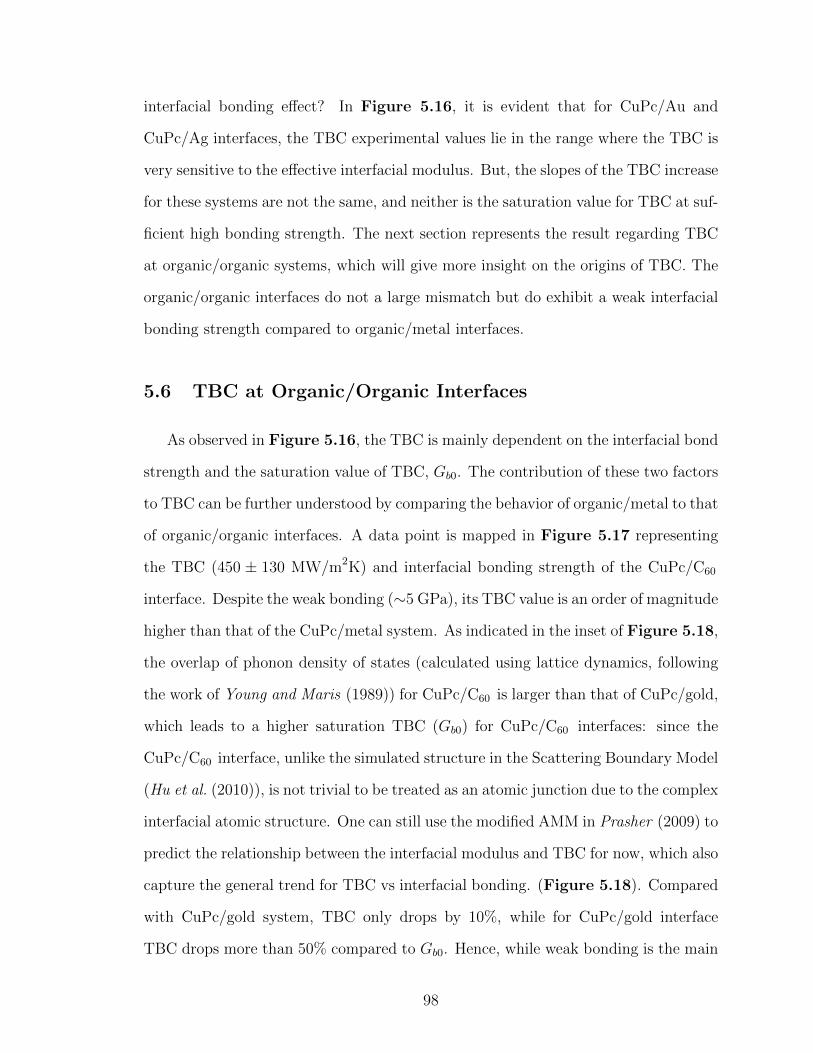
interfacial bonding effect? In Figure 5.16, it is evident that for CuPc/Au and
CuPc/Ag interfaces, the TBC experimental values lie in the range where the TBC is
very sensitive to the effective interfacial modulus. But, the slopes of the TBC increase
for these systems are not the same, and neither is the saturation value for TBC at suf-
ficient high bonding strength. The next section represents the result regarding TBC
at organic/organic systems, which will give more insight on the origins of TBC. The
organic/organic interfaces do not a large mismatch but do exhibit a weak interfacial
bonding strength compared to organic/metal interfaces.
5.6 TBC at Organic/Organic Interfaces
As observed in Figure 5.16, the TBC is mainly dependent on the interfacial bond
strength and the saturation value of TBC, Gb0. The contribution of these two factors
to TBC can be further understood by comparing the behavior of organic/metal to that
of organic/organic interfaces. A data point is mapped in Figure 5.17 representing
the TBC (450 ± 130 MW/m2K) and interfacial bonding strength of the CuPc/C60
interface. Despite the weak bonding (∼5 GPa), its TBC value is an order of magnitude
higher than that of the CuPc/metal system. As indicated in the inset of Figure 5.18,
the overlap of phonon density of states (calculated using lattice dynamics, following
the work of Young and Maris (1989)) for CuPc/C60 is larger than that of CuPc/gold,
which leads to a higher saturation TBC (Gb0) for CuPc/C60 interfaces: since the
CuPc/C60 interface, unlike the simulated structure in the Scattering Boundary Model
(Hu et al. (2010)), is not trivial to be treated as an atomic junction due to the complex
interfacial atomic structure. One can still use the modified AMM in Prasher (2009) to
predict the relationship between the interfacial modulus and TBC for now, which also
capture the general trend for TBC vs interfacial bonding. (Figure 5.18). Compared
with CuPc/gold system, TBC only drops by 10%, while for CuPc/gold interface
TBC drops more than 50% compared to Gb0. Hence, while weak bonding is the main
98

limiting factor for TBC for the VTE deposited CuPc/metal interfaces, for systems
with a small mismatch like CuPc/C60 , interface bonding effects appear to be less
significant.
Figure 5.18: Plots of the normalized TBC versus varying modulus at the interface forCuPc/Au and CuPc/C60 . The arrows are pointed to the TBC of thecorresponding bonding strength at the interface of each systems. Theinset represents the DOS of metal, C60 and CuPc calculated using latticedynamics (acoustic phonon only). (Figure from Jin et al. (2012))
5.7 Other Supporting Evidence
Besides CuPc/C60 and CuPc/metal interfaces, Thermal conductivities were mea-
sured for chloro-subphtalocyaninato boron(III) (SubPc)/metals, C60 /metals and Sub-
Pc/C60 multilayer structures. Figure 5.19 and Figure 5.20 present the results for
these measurements. C60 /Ag shares similar slope with CuPc/Ag while the slope rep-
resents the TBC (Eq 3.3). For SubPc/metal interfaces, limited samples are tested
without varying the layer thickness. Compare with the previous CuPc/metals re-
sults, these few data points match well with CuPc/metal, suggesting similar TBC.
For organic/organic interfaces, the thermal conductivities of multilayers are close to
99
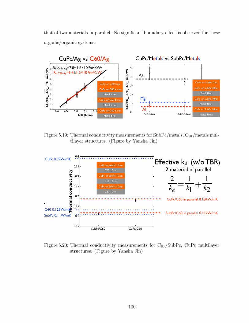
that of two materials in parallel. No significant boundary effect is observed for these
organic/organic systems.
Figure 5.19: Thermal conductivity measurements for SubPc/metals, C60 /metals mul-tilayer structures. (Figure by Yansha Jin)
Figure 5.20: Thermal conductivity measurements for C60 /SubPc, CuPc multilayerstructures. (Figure by Yansha Jin)
100

5.8 Summary
The thermal boundary conductance of CuPc/metal (Al, Ag, Au, Mg) system is
found to be closely correlated to the bonding strength at the organic semiconductor-
metal interface. Molecular dynamics calculations of TBC were performed on these
systems with varying interface bonding strength. Combining MD simulations with
the experimentally measured values of TBC, an effective interface modulus was ex-
tracted for each system, showing results consistent with adhesion tests. Finally,
organic/organic interfaces were studied; regardless of the similar bonding strength
between the organic/metal and organic/organic systems, the latter exhibits an order
of magnitude higher TBC due to the larger overlap in the acoustic phonon spectrum
between CuPc and C60 , suggesting that the TBC of the organic-organic interface is
less sensitive to bonding. In conclusion, one need to have a comprehensive knowledge
of the material acoustic properties (Phonon DOS, sound velocity) and the interfacial
bonding strength to accurately evaluate the thermal boundary conductance of the
corresponding material system. For van der Waals interfaces (effective bonding mod-
ulus: 1∼10 GPa) that have a small DOS overlap, interfacial bonding is the major
factor in boundary phonon transmission; while the systems have less mismatch, the
TBC is still dominated by acoustic properties.
101

CHAPTER VI
Origins of TBC: Anharmonicity and Spatial
Non-Uniformity
6.1 Introduction
In the previous chapter, different analytical models and computer simulation tech-
niques were discussed in items of their ability in calculating the Thermal Boundary
Conductance (TBC) of interfaces involving disordered organics. The limitations of
these techniques are also presented, and it is believed that the Molecular Dynamics
Simulations (MDS) is the most comprehensive and accurate way to analyze the TBC.
However, despite the accuracy of the MDS, it can be time-consuming for systems
involving complicated molecules such as CuPc. Developing a better analytical model
that considers other important factors such as interfacial bonding, can help character-
izing the interfacial thermal transport and assisting prescreening materials in device
design, such as thermoelectric and optoelectronic devices.
In this chapter, the discussion starts with the comparison between the mismatch
models (Section 5.3.1) and MDS (Section 5.3.4) on the CuPc/metal interfaces,
aiming to extract the missing physics for the current analytical models.
Specifically, there are two central influence on TBC at organic/metal interfaces
that cause the inaccuracy of the analytical models like the Modified AMM. One is
102

the anharmonic phonon transmission processes discussed in Section 5.3: the con-
tribution from the anharmonic processes to TBC is extracted from MDS and will
be presented in Section 6.3. Another important factor is the spatial non-uniform
phonon transmission, which has been never proposed in any material systems before.
The evidence for this spatial non-uniform transmission also examined by MDS by
analyzing the displacements of the atoms near the interface, see Section 6.4.
6.2 Mismatch Models with Interfacial Bonding Modifications
It has been widely realized that the mismatch models are not adequate to describe
the physical processes of the interfacial thermal transport. Especially for interfaces
such as organic semiconductor and metal, whose bonding is weak and material mis-
match is large, the interfacial bonding strength is the main influence in thermal trans-
port across the interface. By modifying the expression of transmission coefficient, this
bonding influence can introduced to both AMM and DMM. The former was discussed
in Prasher’s work, the interfacial bonding is represented by the harmonic spring, with
spring constant Ksp. The transmission coefficient, τAMM,K is expressed as, (re-wrote
Eq 5.2)
τAMM,K(ω) =4ZoZm
(Zo + Zm)2 + Z2oZ
2mω2
NintK2sp
(6.1)
the above transmission coefficient is frequency dependent, indicating the interfacial
spring behaves differently according to the phonon frequency. Several works have de-
scribed the physics as the low-pass filter, thus, we could also modify the transmission
coefficient as follows,
τDMM,K(ω) =γ2
γ2 + (ω − ωint)2τDMM (6.2)
103

the pre-multiplier is in form of a damped oscillator, centered at ωint =Ksp
(MoMm)1/2,
where γ/2 is the damping constant. γ2 = 1025 is estimated based on the definition
that at ωint ± γ/2, amplitude is reduced to half the value of the peak.
Figure 6.1 presents the measured and modeled Gb of varies organic semicon-
ductor and metal interfaces. The crystal structures of these organic semiconductor
molecules are also shown in top panel of Figure 6.1. Gb values predicted by the
above mismatch models are presented in the bottom plot. The interfacial spring
constant is derived from the effective modulus at the interface obtained in our previ-
ous publication. Note that AMM and DMM without bonding modifications are far
from satisfactory, while DMM has a closer prediction. This is because the interfa-
cial roughness in the measured structure is around 2 nm, and the coherent phonon
length, Lcoh = ~v/kBT of CuPc, for example, is around 5 A. As a result, the phonon
scattering at the interface is pure diffuse in nature. The weak interfacial bonding
between organic semiconductor and metal will lead to deduction in Gb and achieve
much closer estimation of Gb, see Figure 6.1.
However, introducing Ksp appears to be an over correction. A comparison between
these models and the Molecular Dynamic Simulations (MDS) on CuPc/Ag interface
is shown in Figure 6.2; AMM+Ksp generally agrees with MDS than DMM+Ksp;
This is due to the fact that in MDS simulation, the interface is perfectly flat, and the
formalism confined the transmission as specular. The discrepancy at low interfacial
bonding strength regime applies for both models, where the experimental data lies.
This overcorrection is attribute to the lack of consideration of the anharmonic phonon
transmission.
104

Figure 6.1: (Top) Drawings of the structure of three small-molecule organic semicon-ductors involved in this work. (Bottom) Thermal boundary conductance(Gb) values of the organic semiconductor and metal interfaces measuredexperimentally, modeled by AMM and DMM; along with the modeledvalues of modified AMM and DMM considering the interfacial bondingstrength, whose effect is represented by the interfacial spring constantKsp.
105

Figure 6.2: Thermal boundary conductance of CuPc/Ag versus interfacial spring con-stant, calculated by Molecular Dynamics Simulations (MDS), AMM andDMM with bonding modification. The discrepancy between MDS andAMM+Ksp and DMM+Ksp at lower bonding strength is due to the an-harmonic phonon transmissions. The measured TBC (marked with thegreen star) lies within regime with large anharmonic contribution.
106

6.3 Anharmonic Contribution to Interfacial Thermal Trans-
port
The anharmonic transmission have been discussed in several works and proved to
be important in interfacial thermal transport. However, recall Eq. 6.1 and Eq. 6.2,
both models assume a single harmonic spring constant connecting the two materials.
The phonon frequency stay the same before and after the transmission. The anhar-
monic processes are overlooked. On the other hand, molecular dynamics simulation
can provide a more comprehensive description of atomic interaction potential, in-
cluding the anharmonic contribution. Moreover, MDS work on the material systems
studied this work have been proved to be accurate in predicting Gb. Thus, here in
this work, the anharmonic contribution is extracted from the simulation collection of
molecular dynamics.
Figure 6.3: Top view (Top) and side view (Bottom) of the CuPc-metal interfaces inmolecular dynamics simulation collection.
107

The CuPc/Metal (Ag, Al, Au) interface simulated by MDS is presented in Fig
6.3. The interfacial bonding potential is in form of the Lenard-Jones 9-6 potential
(Eq 5.10).
Expanding this potential around the equilibrium position r0, using the Taylor
expansion formalism yields,
UvdW = U0 +1
2Ksp(∆r)2 +
1
6κ(∆r)3 +O(∆r)3 (6.3)
where
Ksp =d2Uvdw
dr2
∣∣∣∣r=r0ij
and κ =d3Uvdw
dr3
∣∣∣∣r=r0ij
(6.4)
∆r is the displacement to equilibrium position, Ksp is the interfacial spring constant,
κ is the thermal expansion coefficient of the interface. In Eq 6.3, the third term,
16κ(∆r)3, is the leading term that stands for the anharmonic phonon transmission -
the three phonon processes. A three phonon process involves two phonons on one side
of the interface which combine and emit one phonon at the other side of the interface.
Previous work shows these inelastic processes provide an extra tunnel for thermal
transport thus increase the TBC (Hopkins et al. (2011); Stevens et al. (2007); Hopkins
(2009)). In this thesis, the contribution from the anharmonic processes is estimated
using the ratio of anharmonic energy Ua to the total energy Utot = UvdW − U0, with
a re-defined energy zero point at U0),
UaUtot
=16κ(∆r)3
16κ(∆r)3 + 1
2Ksp(∆r)2
=κ∆r
κ∆r + 3Ksp
(6.5)
Apply Eq 6.5 to LJ 9-6 potential, the anharmonic energy ratio, Ua/Utot, can be
rewritten as,
UaUtot
=972
∑i, jχεij(r
0ij)−3
972∑i, jχεij(r0
ij)−3 + 162
∑i, jχεij(r0
ij)−2∼ 6〈∆r〉
6〈∆r〉+ d0
(6.6)
108

Figure 6.4: Anharmonic contribution percentage (Blue) in interfacial pair potentialversus interfacial bond ratio (χ). The AMM+Ksp deviation from MDSversus the interfacial bond ratio (Green) scales with the anharmonic en-ergy percentages. The higher the bond ratio, the less the atoms movementperpendicular to the interfaces (∆z), shown in the bottom image series.
109

Fig 6.4 presents the anharmonic energy percentage (Eq 6.6) versus the interfacial
bonding ratio, χ. Note that the lower the interfacial bonding, the higher the per-
centage. This is due the high vibration amplitude, ∆z, at low bonding strength, see
bottom of Fig 6.4, while atoms at the interface move out of the anharmonic zone and
anharmonic transmission processes have to be taken into consideration as a result.
Previous work shows these anharmonic processes provide an extra tunnel for thermal
transport thus increase the TBC (Hopkins et al. (2011); Stevens et al. (2007); Hopkins
(2009)). The green curve in Fig 6.4 represents the amount that Gb-MDS is larger
than Gb- AMM+Ksp. The differences scale proportionally with the anharmonic en-
ergy percentage, suggesting the anharmonic phonon transmission is a crucial factor
that mismatch models have been neglecting.
6.4 Spatially Non-Uniform Phonon Transmission
Figure 6.5: Plot of TBC versus effective modulus at the interface of CuPc-Al in-terfaces. AMM and MDS do not match each other like CuPc-Ag andCuPc-Au. (Figure from Yansha Jin)
However, in the case of CuPc-Al, the fitting between Prasher (2009) and MD
simulation is not satisfactory. The saturated TBC value Gb0 does not match with
110

Figure 6.6: Spatial distribution of the average displacements of the 1st layer CuPc(a) at the CuPc-Al interface, (b) at CuPc-Au interface; For CuPc-Alinterface, the atoms at the center of the CuPc molecule are more confinedthan other atoms at the side of the molecule, indicating a spatial non-uniformity. (Figure by Yansha Jin)
each other (See Figure 6.5). This could potentially be explained by the break-down
of spatially uniform transmission assumption in all existing analytical models. When
we compared the average displacement of CuPc-Al in Figure 6.6 (a) and CuPc-Au in
Figure 6.6 (b) under same bond ratio 1.25, it is evident that the spatial distribution
of vibration amplitude of atoms are uniform at CuPc-Au interface, while in case of
CuPc-Al, though the average amplitude is smaller, the center of the molecule (features
near the copper atoms) are more confined than other atoms in the same molecule.
Assuming a spatial uniform transmission coefficient at the CuPc-Al interface is not
valid according to this analysis. Unlike CuPc/Ag and CuPc/Au, the saturation TBC
of CuPc/Al interfaces is only 1/4 of the predicted value of the modified acoustic
mismatch model. After extracting the movements of each atom of the 1st layer CuPc
near the interface in the MD simulation, we find that when heat is transported across
the CuPc/Al interfaces, within the CuPc molecule, the center atom displacements
are smaller than C and H atoms at the side which means the bonding strength to
the Al atoms is different. This spatial non-uniformity effect is only significant for
111

CuPc/Al, but not for CuPc/Ag and CuPc/Au and could potentially explain the
overestimation of TBC calculated by the mismatch models. After considering the
spatial non-uniformity by taking into account the transmission of each atoms, the
predicted TBC is more closely matched to the experimental value and the value
obtained by MD simulation.
Figure 6.7: TBC has a non-linear dependence on the interfacial bonding strength.The average spring constants for CuPc/Al and CuPc/Ag are mappedin theses plot, respectively. Using this average spring constant lead toinaccurate prediction for TBC of CuPc-Al, since the TBC dependence isnot linear and using arithmetic average of spring constant in the models,such as the Modified AMM can be problematic. (Figure by Yansha Jin)
To estimate the contribution of spatial non-uniformity in atomic vibrations to
lowering TBC, we averaged individual Ksp values in randomly distributed sampling
circles 1 nm in diameter (corresponding to the phonon mean free path of CuPc).
Figure 6.7 illustrate the reason why using the average Ksp spatially can be prob-
lematic. TBC’s dependence on Ksp is not linear, simply averaging Ksp before cal-
culating TBC does not return the accurate average TBC. Thus, we calculated TBC
at each position using the sampled Ksp within the phonon mean free path of CuPc,
then take the average. The illustration of this process is shown in Figure 6.8, and
the result is shown in Table 6.1.
Our model shows better agreement with experimentally measured TBC values, as
112

Figure 6.8: Illustration of TBC calculation considering the spatial non-uniform effect.TBC is calculated separately for each atom, then sampled in the circleswith radii of CuPc’s phonon mean free path. (Figure by Yansha Jin)
CuPc/Aluminum CuPc/Gold
MDS(in agreement w/ exp.) 70 ± 5 MW/m2K 46 ± 6 MW/m2K
ModifiedAMM 201 MW/m2K 52 MW/m2K
Model w/ bondingnon-uniformity 94 MW/m2K 44 MW/m2K
Table 6.1: TBC for CuPc/Al and CuPc/Au calculated by MDS; Modified AMM;Analytical model considering bonding and spatial non-uniformity.
well as with MD simulated TBC values than other models, suggesting that phonon
transmission is indeed strongly influenced by spatial non-uniformity of bonding and
atomic vibrations at the interface.
113

CHAPTER VII
Summary and Future Directions
7.1 Doctoral Research Summary
My doctoral research work is one of the first reports on the measurements of the
thermal boundary conductance values at organic/metal interfaces. (Ch. III) I fab-
ricated multilayer films consisting of an archetypal organic semiconductor, CuPc and
metals(Al, Ag) by vacuum thermal evaporation. The TBC values for such interfaces
are shown to be as low as 13 MW/m2K, (Jin et al. (2011)) strongly suggesting the no-
table interfacial contribution to the thermal transport in nano-structured materials.
Quantifying this interfacial contribution is thus extremely essential for the advance of
energy conversion applications and the thermal managements for organic electronic
device. For example, the TBC values reported by my work are then considered to be
a crucial factor in accurate temperature-dependent modeling on the performances of
organic light-emitting diodes.(Qi and Forrest (2011); Bergemann et al. (2012))
As for the thermoelectric applications (Ch. IV), the thermally resistive nature of
these interfaces can provide us a novel way for tuning the thermoelectric properties of
composite materials.(Jin et al. (2013)) Our simulations and experiments show that in
the CuPc/Ag composite, the percolation threshold for thermal transport xc,th% shifts
to a higher concentration compared to that for electrical transportxc,e% due to the
low thermal boundary conductance and the high electrical boundary conductance. A
114
maximum ratio of electrical conductivity σe over thermal conductivity kth is observed
near xth,min, the volume fraction that reaches the lowest kth. This maximum ratio
is 3 times larger than that of pure CuPc, potentially increasing the thermoelectric
figure of merit by more than a factor of 10 times for organic TE materials. This
dramatically increased performance potential calls for a composite system with high
thermal boundary resistance but low electrical contact resistance, which is more easily
achievable, and can allow σe/kth to be maximized in the regime where S, Seebeck
coefficient is relatively stable.
I have also investigated the fundamental physics of the TBC at the interfaces in-
volving small-molecule organics based on our observation of the low TBC at CuPc/metal
interfaces.(Ch. V) I found that for highly mismatched interfaces like organics/metal,
the TBC was closely correlated to the bonding strength at the interface. Evidence
from Molecular Dynamics Simulations (MDS) also showed the significant impact of
interfacial bonding on TBC. I also examined the TBC of the organic/organic inter-
faces and the measured TBC values of these interfaces suggested that regardless of the
similar bonding strength between organic/metal and organic/organic systems. The
latter exhibited an order of magnitude higher TBC due to the larger overlap in the
acoustic phonon spectrum between the organics, indicating that low mismatched sys-
tems are not as sensitive to the interfacial bonding strength. The thermal property
mismatch and interfacial bonding are now widely accepted as the two dominating
factors that are attributed to the TBC, and our work is one of the first experimental
demonstrations of the bonding effect.
Aside from the two aspects of thermal boundary transport discussed above, which
can be applied to all general interfaces, we found another central influence on our
specific small-molecule organics/metal system: spatially non-uniform transmission.
(Chap VI) The physical models with interfacial bonding modifications can produce
results similar to the MD simulations and the experiments. However, in some systems
115

like CuPc/Al, the predicted TBC deviates from the exact value, suffering a 3-time
overestimation. This discrepancy is attributed to the spatially non-uniform phonon
transmission verified by extracting the movements of the interfacial atoms in the
MD simulations. By adding in this factor to the existing model, the accuracy of the
phonon transmission modeling was drastically improved, with the margin of error was
reduced to 25%. This work presented a more rigorous way in analyzing the thermal
transport at van der Waals interfaces.
In conclusion, organic/metal interfaces are ubiquitous in organic electronics and
thermoelectric devices and can have a strong influence on the overall behavior of
those devices. Our work can provide some new approaches for optimizing the device
performances that have been discussed as well as some fundamental insights into the
microscopic mechanisms of phonon coupling across interfaces. The following section
presents the outlook regarding follow-on.
7.2 Future Work Proposals
7.2.1 Interfacial Science in Organic Electronic Devices
Electronic devices based on organic semiconductor with metal nanoparticles (NP)
incorporated have been demonstrated, such as memory elements, photodetectors (Guo
et al. (2012)) and transistors (Tseng and Tao (2009)). The nanostructure are similar
to the nanocomposites for thermoelectric applications discussed in Chap IV. Charges
trap/de-trap rate in organic FET memory devices is crucial to the speed of the device.
Exploring the charge trapping mechanism while tuning the phonon modes at the
NPs/organic interfaces is a promising plan, considering the strong coupling between
the phonon modes and charge carrier transport.
116

7.2.2 Thermal Stability of Organic Electronics in Bio-Medical Applica-
tions
Considerable amount of research on organic electronics are focus on bio-medical
applications due to the mechanical flexibility and bio-compatibility of the organic
materials. One of the major problem is the the thermal stability of the organic device
(Kuribara et al. (2012)). Temperature of sterilization processes can be as high as 121
Celsius, and the thermal stability of organic material under this condition is crucial
for the device operations. Thermal property measurements and system analysis of
the device can be obtained using the methods in this thesis, (Chap III and Chap
I) that can be valuable in understanding the thermal stability of organic electronic
device for bio-medical applications.
7.2.3 Thermal Transport in Carbon Nanoelectronics
Carbon-nanoelectronic devices are becoming increasingly widespread. However,
most of its thermal properties are derived from those of graphite, but the heat dis-
sipation in these devices are primarily limited by the edges and the in-plane van der
Waals bonds that are not considered as a bulk.(Baloch et al. (2010, 2012); Pop et al.
(2012)) My study on thermal boundary conductance at van de Waals interfaces can
bring new understanding in this area and potentially create a novel way in tuning the
thermal properties of graphene/CNT devices with interface/surface treatments.
117

APPENDICES
118

APPENDIX A
Dimer of Two-Level Molecules
This Appendix is based on the book of Agranovich and Bassani (2003).
Let’s start with the Hamiltonian for a single molecule. Assume a two-level molecule
system: |g〉 – ground state; |e〉 – excited state.
Hmol = ~ωg|g〉〈g|+ ~ωex|e〉〈e| (A.1)
In the solid phase, there are more than one molecule so that the intermolecular
interactions have to be considered. The simplest illustration of solid is a dimer system:
Hdim = Hmol,1 + Hmol,2 + V1,2 (A.2)
V1,2 is supposed to contain all the Coulomb interactions among excitons and nuclei
between molecule 1 and 2 rigorously, but the exciton-exciton interaction is often
ignored for simplicity.
The dimer system has four energy states: |g1g2〉, |e1g2〉, |g1e2〉 and |e1e2〉. |e1g2〉,
|g1e2〉 are degenerated and have notable interactions in between. All other cross-
interactions are negligible compared to the |e1g2〉, |g1e2〉 interactions. The Hamilto-
119

nian can be re-written as:
Hdim = 2Eg +
|g1g2〉 |e1g2〉 |g1e2〉 |e1e2〉
〈g1g2| Vgg,gg 0 0 0
〈e1g2| 0 Eex + Veg,eg J12 0
〈g1e2| 0 J12 Eex + Vge,ge 0
〈e1e2| 0 0 0 2Eex + Vee,ee
(A.3)
where Eg = ~ωg and Eex = ~ωex. Vab,cd = 〈ab|V1,2|cd〉 and J12 = 〈g1e2|V1,2|e1g2〉
is a special quantity representing the intermolecular overlap integral under certain
assumptions.
The new eigenstates, |±〉, are the linear combinations of the degenerated states:
|±〉 = (|e1g2〉 ± |g1e2〉)/√
2 (A.4)
with new energy levels
E± = ~ωex + (Veg,eg − Vgg,gg)± J1,2 (A.5)
120

APPENDIX B
Polaron Transport Model
This model follows the work of Ortmann et al. (2009).
Though this model does not take lattice disorder into account, it describes the
charge transport with both coherent and hopping contribution included. Starting
with the polaron Hamiltonian in Eq 1.18 and adopting the Green-Kubo formalism,
the mobility yields,
µGK =1
2eNckBT
∞∫−∞
dt〈j(t)j(0)〉H (B.1)
And since the current density j and the polarization P = e∑M
RMa†MaM relate by
j = dPdt
, j can be written as,
j =1
i~[P, H] =
e
i~∑MN
(RM −RN)JMNa†MaN (B.2)
The approach in Ortmann et al. (2009) is the polaron transform in form of,
H = eSHeS†, where S =
∑MQ
gQMMa†MaM(b†Q − b−Q) (B.3)
121

Thus,
H =∑MN
a†MEMNaN +∑Q
~ωQ
(b†QbQ +
1
2
)(B.4)
where EMN = eCMεMNe−CN and CM =
∑Q
gQMM(b†Q − b−Q) Use the thermal average
of the transfer integral
εMN = εMN exp
[−∑Q
(1
2+NQ
)|gQMM − g
QNN|
2
](B.5)
The Hamiltonian yields,
H =∑MN
a†MεMNaN +∑Q
~ωQ
(b†QbQ +
1
2
)(B.6)
Define the thermal average 〈 〉H as
〈 j(t)j(0) 〉H =Tr(e−(H/kBT )j(t)j(0))
Tr(e−(H/kBT ))(B.7)
with Eq B.2 and Eq B.7, the mobility (Eq B.1) splits into two terms,
µ = µcoh + µinc (B.8)
µcoh =
√πeτe
2NckBT
∫k
nk(1− nk)(v∗)2dk (B.9)
µinc =e
2NckBT~∑R
(RJR)2 1
NΩ
(B.10)
×∫
k1k2
nk2(1− nk2)dk1k2
∞∫∞
dte(it/~)[J(k1)−J(k2)]
× exp2∑Q
[NQeiωQt + (1 +NQ))gQ]− 1e−(t/τe)2
122
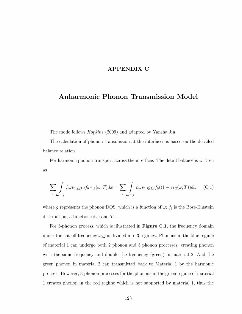
APPENDIX C
Anharmonic Phonon Transmission Model
The mode follows Hopkins (2009) and adapted by Yansha Jin.
The calculation of phonon transmission at the interfaces is based on the detailed
balance relation.
For harmonic phonon transport across the interface. The detail balance is written
as
∑j
∫ωc,1,j
~ωv1,jg1,jf0τ1,2(ω, T )dω =∑j
∫ωc,2,j
~ωv2,jg2,jf0((1− τ1,2(ω, T ))dω (C.1)
where g represents the phonon DOS, which is a function of ω; f) is the Bose-Einstein
distribution, a function of ω and T .
For 3-phonon process, which is illustrated in Figure C.1, the frequency domain
under the cut-off frequency ωc,2 is divided into 3 regimes. Phonons in the blue regime
of material 1 can undergo both 2 phonon and 3 phonon processes: creating phonon
with the same frequency and double the frequency (green) in material 2; And the
green phonon in material 2 can transmitted back to Material 1 by the harmonic
process. However, 3-phonon processes for the phonons in the green regime of material
1 creates phonon in the red regime which is not supported by material 1, thus the
123

Figure C.1: Schematic drawing of detailed balance of 3-phonon process. (Figure fromYansha Jin)
reverse transmission is forbidden. The detailed balance of the 3-phonon processes is
written as,
2(~ω)v1,jg1,jf0(1− τ (2)12 )τ
(3)12 = h(2ω)v2.jg2,jf0τ
(2)12 (1− τ (3)
12 ) (C.2)
when 0 < ω < ωc,1,j/2;
2(~ω)v1,jg1,jf0(1− τ (2)12 )τ
(3)12 = h(2ω)v2.jg2,jf0(1− τ (3)
12 ) (C.3)
when ωc,1,j/2 < ω < ωc,1,j;
Figure C.2: Schematic drawing of detailed balance of 4-phonon process. (Figure fromYansha Jin)
124

The schematic drawing of 4-phonon process is shown in Figure C.2, and the
generalized n phonon process is shown in Hopkins (2009).
125

BIBLIOGRAPHY
126

BIBLIOGRAPHY
Adamovich, V. I., M. S. Weaver, R. C. Kwong, and J. J. Brown (2005), High Temper-ature Operation and Stability of Phosphorescent OLEDs, Current Applied Physics,5, 15.
Agranovich, V., and G. Bassani (2003), Electronic Excitations in Organic BasedNanostructures, 1st ed., 5-20 pp., Elsevier Academic Press.
Agrawal, K., M. E. Sykes, and M. Shtein (2013), Influence of Exciton Lifetime onCharge Carrier Dynamics in an Organic Heterstructure, Applied Physics Letters,102, 113,304.
Aıch, R. B., N. Blouin, A. Nouchard, and M. Leclerc (2009), Electrical and Ther-moelectric Properties of poly(2,7-carbazole) Derivatives., Chemical Materials, 24,751.
Antohe, S., N. Tomozeiu, and S. Gogonea (1991), Properties of the Organic-on-Inorganic Semiconductor Barrier Contact Diodes In/PTCDI/p-Si and Ag/CuPc/p-Si, Physica Status Solidi (a), 125, 397–408.
Ashcroft, N. W., and N. D. Mermin (1976), Solid State Physics, 1st ed., 1-212 pp.,Harcourt College Publishers.
Baldo, M. (2001), The Electronic and Optical Properties of Amorphous Organic Semi-condutors, Princeton University (Disseration).
Baloch, K. H., N. Voskanian, and J. Cumings (2010), Controlling the Thermal Con-tact Resistance of a Carbon Nanotube Heat Spreader, Applied Physics Letters, 97,063,105.
Baloch, K. H., N. Voskanian, M. Bronsgeest, and J. Cumings (2012), Remote JouleHeating By a Carbon Nanotube, Nature Nanotechnology, 7, 316.
Bassler, H. (1993), Charge Transport in Disordered Organic Photocunductors Simu-lation Study, Physica Status Solidi (b), 1, 15.
Bergemann, K. J., R. Krasny, and S. R. Forrest (2012), Thermal Properties of OrganicLight-Emitting Diodes, Organic Electronics, 12, 1565.
127

Borca-Tasciuc, T., A. R. Kumar, and G. Chen (2001), Data Reduction in 3ω Methodfor Thin-Film Thermal Conductivity Determination, Review of Scientific Instru-ments, 72, 2139.
Bubnova, O., Z. U. Khan, A. Malti, S. Braun, M. Fahlman, M. Berggren, andX. Crispin (2011), Optimization of the Thermoelectric Figure of Merit in the Con-ducting Polymer Poly(3,4-ethylenedioxythiophene), Nature Materials, 10, 429.
Cahill, D. G. (1990), Thermal Conductivity Measurement From 30 to 750 K: The 3ωMethod, Review of Scientific Instruments, 61, 802.
Cahill, D. G. (2004), Analysis of Heat Flow in Layered Structures for Time-DomainThermoreflectance, Review of Scientific Instruments, 75, 5119.
Chung, S., J.-H. Lee, J. Jeong, J.-J. Kim, and H. Yongtaek (2009), Substrate ThermalConductivity Effect on Heat Dissipation and Lifetime Improvement of OrganicLight-Emitting Diodes, Applied Physics Letters, 94, 253,302.
Coropceanu, V., J. Cornil, D. da Silva Filho, Y. Oliver, R. Silbey, and J. Bredas(2007), Charge Transport in Organic Semiconductor, Chemical Review, 107, 926.
Costescu, R. M., D. G. Cahill, F. H. Fabreguette, Z. A. Sechrist, and S. M. George(2004), Ultra-Low Thermal Conductivity in W/Al2O3 Nanolaminates, Science, 303,989.
Cutler, M., J. F. Leavy, and R. I. Fltzpartick (1964), Electronic Transport inSemimetallic Cerium Sulfide., Physical Review, 133, 1143.
Daly, B. C., H. J. Maris, W. K. Ford, G. A. Antonelli, L. Wong, and E. Andideh(2002), Optical Pump-Probe Measurements of Sound Velocity and Thermal Con-ductivity of Hydrogenated Amorphous Carbon Films, Journal of Applied Physics,92, 6005.
Duong, H. M., D. V. Papavassiliou, K. J. Mullen, and S. Maruyama (2008), Com-putational Modeling of the Thermal Conductivity of Single-Walled Carbon Nan-otubePolymer Composites, Nanotechnology, 19, 065,702.
Efremov, A. A., N. I. Bochkareva, R. I. Gorbunov, D. A. Lavrinovich, Y. T. Rebane,T. D. V., and S. Y. G. (2006), Effect of the Houle Heating on the Quantum Effi-ciency and Choice of Thermal Condition for High-Power Blue InGaN/GaN LEDs,Physics of Semiconductor Devices, 40, 621.
Fox, M. (2001), Optical Properties of Solids, 1st ed., 76-222 pp., Oxford University.
Guo, F., B. Yang, Y. Yuan, Z. Xiao, Q. Dong, Y. Bi, and J. Huang (2012), ANanocomposite Ultraviolet Photodetector Based on Interfacial Trap-ControlledCharge Injection, Nature Technology, 7, 798.
128

Hopkins, P. E. (2009), Thermoelectricity in Semiconductor Nanostructures, Journalof Applied Physics, 106, 013,528.
Hopkins, P. E., L. M. Phinney, J. R. Serrano, and T. E. Beechem (2010), Effectsof Surface Roughness and Oxide Layer on the Thermal Boundary Conductance atAluminum/Silicon Interfaces, Physical Review B, 82, 085,307.
Hopkins, P. E., J. C. Duda, and P. M. Norris (2011), Anharmonic Phonon Interactionsat Interfaces and Contributions to Thermal Boundary Conductance, Journal ofHeat Transfer, 133, 062,401.
Hsieh, W.-P., M. D. Losego, P. V. Braun, S. Shenogin, P. Keblinski, and D. G.Cahill (2011), Testing the Minimum Thermal Conductivity Model for AmorphousPolymers using High Pressure, Physical Review B, 83, 174,205.
Hu, L., L. Zhang, M. Hu, J.-S. Wang, B. Li, and P. Keblinski (2010), Phonon Inter-ference at Self-Assembled Monolayer interfaces: Molecular Dynamics Simulations,Physical Review B, 81, 235,427.
Hu, M., P. Kelinski, and P. K. Schelling (2009), Kapitza Conductance of Silicon-Amorphous Polyethylene Interfaces by Molecular Dynamics Simulations, PhysicalReview B, 79, 104,305.
Huang, B. L., Z. Zi, A. Millward, A. McGaughey, C. Uher, M. Kaviany, and O. Yaghi(2007), Thermal Conductivity of a Metal-Organic Framework (MOF-5): Part II.Measurement, International Journal of Heat and Mass Transfer, 50, 405.
Huang, K. (1997), Solid State Physics (Chinese), 1st ed., 76-283 pp., Beijing Univer-sity.
Jin, Y., A. Yadav, H. Sun, K. Sun, K. P. Pipe, and M. Shtein (2011), ThermalBoundary Resistance of Copper Phthalocyanine-Metal Interface, Applied PhysicsLetters, 98, 093,305.
Jin, Y., C. Shao, J. Kieffer, K. P. Pipe, and M. Shtein (2012), Origins of ThermalBoundary Conductance of Interfaces involving Organic Semiconductors, Journal ofApplied Physics, 112, 093,503.
Jin, Y., S. Nola, K. P. Pipe, and M. Shtein (2013), Improving Thermoelectric Effi-ciency in Organic-Metal Nanocomposites via Extra-Low Thermal Boundary Con-ductance, Journal of Applied Physics, 1, 000,000.
Kahn, A., N. Koch, and W. Gao (2003), Electronic Structure and Electrical Proper-ties of Interfaces between Metals and pi-Conjugated Molecular Films, Journal ofPolymer Science, 41, 2529–2548.
Kapitza, P. (1941), Kapitza Resistance, Journal of Physics, USSR, 4.
129

Kim, D., Y. Kim, K. Choi, J. C. Grunlan, and C. Yu (2010), Improved Ther-moelectric Behavior of Nanotube-Filled Polymer Composites with Poly(3,4-ethylenedioxythiophene) Poly(styrenesulfonate), ACS Nano, 4, 513.
Kim, E.-K., S.-I. Kwun, S.-M. Lee, H. Seo, and J.-G. Yoon (2000), Thermal BoundaryResistance at Ge2Sb2Te5/ZnS:SiO2 Interface, Applied Physics Letters, 76, 3864.
Kim, G., K. P. Pipe, and M. Shtein (2011), Thermoelectric and Bulk Mobility Mea-surements in Pentacene Thin Films, Applied Physics Letters, 98, 093,303.
Kim, N., B. Domercq, S. Yoo, A. Christensen, B. Kippelen, and S. Graham (2005),Thermal Transport Properties of Thin Films of Small Molecule Organic Semicon-ductors, Applied Physics Letters, 87, 241,908.
Koh, Y. K., S. L. Singer, W. Kim, J. M. O. Zide, H. Lu, D. G. Cahill, A. Majum-dar, and A. C. Gossard (2009), Comparison of the 3-ω Method and Time-DomainThermoreflectance for Measurements of the Cross-Plane Thermal Conductivity ofEpitaxial Semiconductors, Journal of Applied Physics, 105, 054,303.
Kroger, I., B. Stadtmuller, F. Reinert, and C. Kumpf (2011), Normal-Incidence X-rayStanding-Wave Study of Copper Phthalocyanine Submonolayers on Cu(111) andAu(111), Physical Review B, 83, 195,414.
Kroger, I., et al. (2010), Submonolayer Growth of Copper-Phthalocyanine on Ag(111),New J. Phys., 12, 083,038.
Kuribara, K., et al. (2012), Organic Transistors with High Thermal Stability forMedical Applications, Nature Communications, 3, 723.
Kwok, H. L. (2012), Thermoelectric Power and ZT in Conducting Organic Semicon-ductor, Journal of Electronic Materials, 41, 476.
Leclerc, M., and N. Ahmed (2011), Green Energy From a Blue Polymer, NatureMaterials, 10, 409.
Lee, S.-M., and D. G. Cahill (1997), Heat Transport in Thin Dielectric Films, Journalof Applied Physics, 81, 2590.
Li, Q., C. Liu, and S. Fan (2009), Thermal Boundary Resistances of Carbon Nan-otubes in Contact with Metals and Polymers, Nano Letters, 9, 3805.
Li, X., and R. Yang (2012), Size-Dependent Phonon Transmission Across DissimilarMaterial Interfaces, Physical Review B, 24, 155,302.
Losego, M. D., M. E. Grady, N. R. Sottos, N. R. Cahill, and P. V. Braun (2012),Molecular Dynamics Simulation of Thermal Boundary Conductance between Car-bon Nanotubes and SiO2, Nature Materials, 11, 502.
Majumdar, A. (2004), Thermoelectricity in Semiconductor Nanostructures, Nature,303, 777.
130

Majumdar, A., and P. Reddy (2004), Role of electronphonon coupling in thermalconductance of metalnonmetal interfaces, Appl. Phys. Lett., 84, 4786.
Minnich, A. J., M. S. Dresselhaus, R. Z. F., and C. G. (2009), Bulk nanostructuredthermoelectric materials: current research and future prospects, Energy Environ.Sci., 2, 466.
Ong, Z.-Y., and E. Pop (2010), Molecular Dynamics Simulation of Thermal BoundaryConductance between Carbon Nanotubes and SiO2, Physical Review B, 81, 155,408.
Ortmann, F., F. Bechstedt, and K. Hannewald (2009), Theory of Charge Transportin Organic Crystals: Beyond Holsteins Small-polaron Model, Physical Review B,79, 235,206.
Park, J. W., D. C. Shin, and S. H. Park (2011), Large-Area OLED Lightings andtheir Applications, Semiconductor Science and Technology, 26, 034,002.
Peng, C., L. Cheng, and M. Mansuripur (1997), Experimental and Theoretical In-vestigations of Laser-induced Crystallization and Amorphization in Phase-ChangeOptical Recording Media, Journal of Applied Physics, 82, 4183.
Pollack, G. L. (1969), Kapitza Resistance, Review of Modern Physics, 41, 48.
Pop, E., V. Varshney, and A. K. Roy (2012), Thermal Properties of graphene: Fun-damentals and applications, MRS Bulletin, 37, 1273.
Prasher, R. (2009), Acoustic Mismatch Model for Thermal Contact Resistance of vander Waals Contacts, Applied Physics Letters, 94, 041,905.
Qi, X., and S. R. Forrest (2011), Thermal Analysis of High Intensity Organic Light-Emitting Diodes Based on a Transmission Matrix Approach, Journal of AppliedPhysics, 110, 124,516.
Ranninger, J. (2006), Introduction to Polaron Physics: Basic Concepts and Models,arXiv:cond-mat, 1, 0606,665.
Schmidt, A. J., M. Chiesa, X. Chen, and G. Chen (2008), An Optical Pump-ProbeTechnique for Measuring the Thermal Conductivity of Liquids, Review of ScientificInstruments, 79, 064,902.
See, K. C., J. P. Feser, C. E. Chen, A. Majumdar, J. J. Urban, and R. A. Segal-man (2010), Water-Processable Polymer-Nanocrystal Hybrids for Thermoelectrics,Nano Letters, 10, 4664.
Shao, C., X. Ma, C. Zheng, Y. Jin, K. P. Pipe, M. Shtein, and J. Kieffer (2013), ForceField Development and Thermal Conductivity Calculation for Copper Phthalocya-nine Molecule, JPPC, 1, 000,000.
Snyder, G. J., and E. S. Toberer (2008), Complex thermoelectric materials, NatureMaterials, 7, 105.
131
Stadler, C., S. Hansen, I. Kroger, C. Kumpf, and E. Umbach (2009), Tuning Inter-molecular Interaction in Long-range-ordered Submonolayer Organic Films, NaturePhysics, 5, 153.
Stevens, R. J., A. N. Smith, and P. M. Norris (2005), Measurement of ThermalBoundary Conductance of a Series of Metal-Dielectric Interfaces by the TransientThermoreflectance Technique, Journal of Heat Transfer, 127, 315.
Stevens, R. J., L. V. Zhigilei, and P. M. Norris (2007), Effects of Temperature andDisorder on Thermal Boundary Conductance at Solid-Solid Interfaces: Nonequi-librium Molecular Dynamics Simulations, International Journal of Heat Transfer,50, 3977.
Stoner, R. J., and H. J. Maris (1993), Kapitza Conductance and Heat Flow BetweenSolids at Temperatures from 50 to 300K, Physical Review B, 48, 16,373.
Sun, H. (2013), Acoustic phonon transport at nanostructured interface, University ofMichigan (Disseration).
Sun, H., V. A. Stoica, M. Shtein, R. Clarke, and K. P. Pipe (2013), Coherent Controlof GHz Resonant Modes by an Integrated Acoustic Etalon, Physics Review Letters,110, 086,109.
Swartz, E. T., and R. Pohl (1989), Thermal Boundary Resistance, Review of ModernPhysics, 61, 605.
Tong, T., and A. Majumdar (2006), Reexamining the 3-omega Technique for ThinFilm Thermal Characterization, Review of Scientific Instruments, 77, 104,902.
Torquato, S., and M. D. Rintoul (1995), Effect of the Interface on the Properties ofComposite Media, Physical Review Letters, 75 (22), 4067–4070.
Tseng, C.-W., and Y.-T. Tao (2009), Electric Bistability in Pentacene Film-BasedTransistor Embedding Gold Nanoparticles, Journal of the American Chemical So-ciety, 131, 12,441.
Venkatasubramanian, R., E. Silvola, T. Colpitts, and B. O’Quinn (2001), Thin-FilmThermoelectric Devices with High Room-Temperature Figures of Merit, Nature,413, 597.
Veres, J., S. D. Ogier, S. W. Leeming, D. C. Cupertino, and S. Mohialdin Khaffaf(2003), Low-k Insulators as the Choice of Dielectric in Organic Filed-Effect Tran-sistor, Advanced Functional Materials, 13, 199.
Wang, D., L. Tang, M. Lomg, and Z. Shuai (2009), First-principles Investigationof Organic Semiconductors for Thermoelectric Applications, Journal of ChemicalPhysics, 131, 224,704.
132

Warta, W., and N. Karl (1985), Hot Holes in Naphthalene: High, Electric-Field-Dependent Mobilities, Physical Review B, 32, 1172.
Yadav, A. (2010), Thermal Physics in Electronic and Optoelectronic Materials andDevices, University of Michigan (Disseration).
Young, D. A., and H. J. Maris (1989), Lattice Dynamical Calculation of the KapitzaResistance between fcc Lattice, Physical Review B, 40, 3685.
Yu, C., K. Choi, L. Yin, and G. J. C. (2011), Light-Weight Flexible Carbon NanotubeBased Organic Composites with Large Thermoelectric Power Factors, ACS Nano,5, 7885.
Zhang, B., J. Sun, H. E. Katz, F. Fang, and R. L. Opila (2010), Promising Thermo-electric Properties of Commercial PEDOT:PSS Materials and Their Bi2Te3 PowderComposites, ACS Applied Materials and Interfaces, 11, 3170.
Zhang, L., P. Keblinski, J.-S. Wang, and B. Li (2011), Interfacial thermal transportin atomic junction, Physical Review B, 83, 064,303.
Zhao, Y., H. A. Kwang, S. Chen, B. O’Connor, K. P. Pipe, and M. Shtein (2007),Localized Current Injection and Submicron Organic Light-Emitting Device on aPyramidal Atomic Force Microscopy Tip, Nano Letters, 7, 3645.
133
![1 Electronic Process in Organic Solids...1.2 Structure Characteristics and Properties of Organic Solids 3phenomena in organic solids [2] . To date, many experimental and theoretical](https://static.fdocuments.us/doc/165x107/613cd4604c23507cb635a1a9/1-electronic-process-in-organic-solids-12-structure-characteristics-and-properties.jpg)


![1 Electronic Process in Organic Solids COPYRIGHTED …1.2 Structure Characteristics and Properties of Organic Solids 3 phenomena in organic solids [2] . To date, many experimental](https://static.fdocuments.us/doc/165x107/61278126da36ba090050fb13/1-electronic-process-in-organic-solids-copyrighted-12-structure-characteristics.jpg)