Thermal conductivity measurements of non-metals …...Thermal conductivity measurements of...
15
Thermal conductivity measurements of non-metals via combined time- and frequency-domain thermoreflectance without a metal film transducer L. Wang, R. Cheaito, J. L. Braun, A. Giri, and P. E. Hopkins Citation: Review of Scientific Instruments 87, 094902 (2016); doi: 10.1063/1.4962711 View online: http://dx.doi.org/10.1063/1.4962711 View Table of Contents: http://scitation.aip.org/content/aip/journal/rsi/87/9?ver=pdfcov Published by the AIP Publishing Articles you may be interested in Accurate measurements of cross-plane thermal conductivity of thin films by dual-frequency time-domain thermoreflectance (TDTR) Rev. Sci. Instrum. 87, 075101 (2016); 10.1063/1.4954969 Examining thermal transport through a frequency-domain representation of time-domain thermoreflectance data Rev. Sci. Instrum. 85, 124903 (2014); 10.1063/1.4903463 Parametric study of the frequency-domain thermoreflectance technique J. Appl. Phys. 112, 103105 (2012); 10.1063/1.4761977 Characterization of thin metal films via frequency-domain thermoreflectance J. Appl. Phys. 107, 024908 (2010); 10.1063/1.3289907 A frequency-domain thermoreflectance method for the characterization of thermal properties Rev. Sci. Instrum. 80, 094901 (2009); 10.1063/1.3212673 Reuse of AIP Publishing content is subject to the terms at: https://publishing.aip.org/authors/rights-and-permissions. Download to IP: 137.54.25.105 On: Thu, 22 Sep 2016 13:57:06
Transcript of Thermal conductivity measurements of non-metals …...Thermal conductivity measurements of...

Thermal conductivity measurements of non-metals via combined time- andfrequency-domain thermoreflectance without a metal film transducerL. Wang, R. Cheaito, J. L. Braun, A. Giri, and P. E. Hopkins Citation: Review of Scientific Instruments 87, 094902 (2016); doi: 10.1063/1.4962711 View online: http://dx.doi.org/10.1063/1.4962711 View Table of Contents: http://scitation.aip.org/content/aip/journal/rsi/87/9?ver=pdfcov Published by the AIP Publishing Articles you may be interested in Accurate measurements of cross-plane thermal conductivity of thin films by dual-frequency time-domainthermoreflectance (TDTR) Rev. Sci. Instrum. 87, 075101 (2016); 10.1063/1.4954969 Examining thermal transport through a frequency-domain representation of time-domain thermoreflectancedata Rev. Sci. Instrum. 85, 124903 (2014); 10.1063/1.4903463 Parametric study of the frequency-domain thermoreflectance technique J. Appl. Phys. 112, 103105 (2012); 10.1063/1.4761977 Characterization of thin metal films via frequency-domain thermoreflectance J. Appl. Phys. 107, 024908 (2010); 10.1063/1.3289907 A frequency-domain thermoreflectance method for the characterization of thermal properties Rev. Sci. Instrum. 80, 094901 (2009); 10.1063/1.3212673
Reuse of AIP Publishing content is subject to the terms at: https://publishing.aip.org/authors/rights-and-permissions. Download to IP: 137.54.25.105 On: Thu, 22 Sep
2016 13:57:06
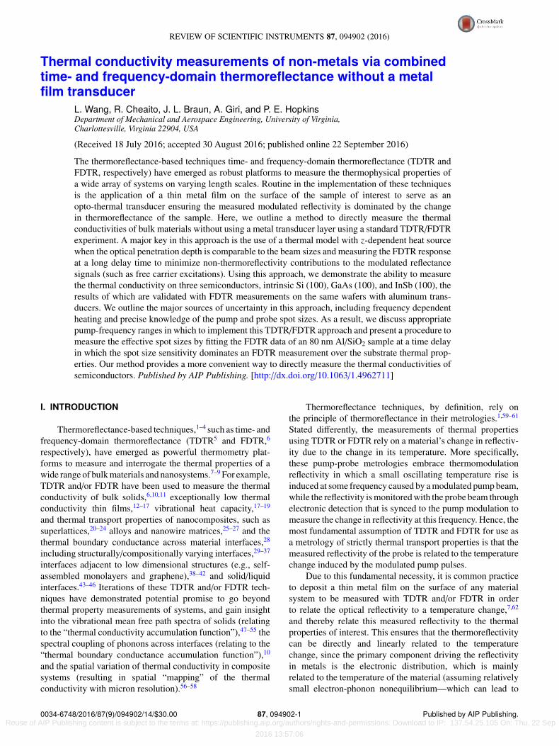
REVIEW OF SCIENTIFIC INSTRUMENTS 87, 094902 (2016)
Thermal conductivity measurements of non-metals via combinedtime- and frequency-domain thermoreflectance without a metalfilm transducer
L. Wang, R. Cheaito, J. L. Braun, A. Giri, and P. E. HopkinsDepartment of Mechanical and Aerospace Engineering, University of Virginia,Charlottesville, Virginia 22904, USA
(Received 18 July 2016; accepted 30 August 2016; published online 22 September 2016)
The thermoreflectance-based techniques time- and frequency-domain thermoreflectance (TDTR andFDTR, respectively) have emerged as robust platforms to measure the thermophysical properties ofa wide array of systems on varying length scales. Routine in the implementation of these techniquesis the application of a thin metal film on the surface of the sample of interest to serve as anopto-thermal transducer ensuring the measured modulated reflectivity is dominated by the changein thermoreflectance of the sample. Here, we outline a method to directly measure the thermalconductivities of bulk materials without using a metal transducer layer using a standard TDTR/FDTRexperiment. A major key in this approach is the use of a thermal model with z-dependent heat sourcewhen the optical penetration depth is comparable to the beam sizes and measuring the FDTR responseat a long delay time to minimize non-thermoreflectivity contributions to the modulated reflectancesignals (such as free carrier excitations). Using this approach, we demonstrate the ability to measurethe thermal conductivity on three semiconductors, intrinsic Si (100), GaAs (100), and InSb (100), theresults of which are validated with FDTR measurements on the same wafers with aluminum trans-ducers. We outline the major sources of uncertainty in this approach, including frequency dependentheating and precise knowledge of the pump and probe spot sizes. As a result, we discuss appropriatepump-frequency ranges in which to implement this TDTR/FDTR approach and present a procedure tomeasure the effective spot sizes by fitting the FDTR data of an 80 nm Al/SiO2 sample at a time delayin which the spot size sensitivity dominates an FDTR measurement over the substrate thermal prop-erties. Our method provides a more convenient way to directly measure the thermal conductivities ofsemiconductors. Published by AIP Publishing. [http://dx.doi.org/10.1063/1.4962711]
I. INTRODUCTION
Thermoreflectance-based techniques,1–4 such as time- andfrequency-domain thermoreflectance (TDTR5 and FDTR,6
respectively), have emerged as powerful thermometry plat-forms to measure and interrogate the thermal properties of awide range of bulk materials and nanosystems.7–9 For example,TDTR and/or FDTR have been used to measure the thermalconductivity of bulk solids,6,10,11 exceptionally low thermalconductivity thin films,12–17 vibrational heat capacity,17–19
and thermal transport properties of nanocomposites, such assuperlattices,20–24 alloys and nanowire matrices,25–27 and thethermal boundary conductance across material interfaces,28
including structurally/compositionally varying interfaces,29–37
interfaces adjacent to low dimensional structures (e.g., self-assembled monolayers and graphene),38–42 and solid/liquidinterfaces.43–46 Iterations of these TDTR and/or FDTR tech-niques have demonstrated potential promise to go beyondthermal property measurements of systems, and gain insightinto the vibrational mean free path spectra of solids (relatingto the “thermal conductivity accumulation function”),47–55 thespectral coupling of phonons across interfaces (relating to the“thermal boundary conductance accumulation function”),10
and the spatial variation of thermal conductivity in compositesystems (resulting in spatial “mapping” of the thermalconductivity with micron resolution).56–58
Thermoreflectance techniques, by definition, rely onthe principle of thermoreflectance in their metrologies.1,59–61
Stated differently, the measurements of thermal propertiesusing TDTR or FDTR rely on a material’s change in reflectiv-ity due to the change in its temperature. More specifically,these pump-probe metrologies embrace thermomodulationreflectivity in which a small oscillating temperature rise isinduced at some frequency caused by a modulated pump beam,while the reflectivity is monitored with the probe beam throughelectronic detection that is synced to the pump modulation tomeasure the change in reflectivity at this frequency. Hence, themost fundamental assumption of TDTR and FDTR for use asa metrology of strictly thermal transport properties is that themeasured reflectivity of the probe is related to the temperaturechange induced by the modulated pump pulses.
Due to this fundamental necessity, it is common practiceto deposit a thin metal film on the surface of any materialsystem to be measured with TDTR and/or FDTR in orderto relate the optical reflectivity to a temperature change,7,62
and thereby relate this measured reflectivity to the thermalproperties of interest. This ensures that the thermoreflectivitycan be directly and linearly related to the temperaturechange, since the primary component driving the reflectivityin metals is the electronic distribution, which is mainlyrelated to the temperature of the material (assuming relativelysmall electron-phonon nonequilibrium—which can lead to
0034-6748/2016/87(9)/094902/14/$30.00 87, 094902-1 Published by AIP Publishing. Reuse of AIP Publishing content is subject to the terms at: https://publishing.aip.org/authors/rights-and-permissions. Download to IP: 137.54.25.105 On: Thu, 22 Sep
2016 13:57:06
094902-2 Wang et al. Rev. Sci. Instrum. 87, 094902 (2016)
nonlinear reflectivities59,60,63—and relatively small strain—which can lead to changes in the piezoreflectance coefficientthat will also impact the changes in reflectivity).64–66 Thisis unlike non-metals where not only temperature but alsoconduction band carrier population can change the reflectiv-ity,67–69 and therefore, the pump excitation in a TDTR and/orFDTR measurement will change both of these components tothe modulated reflectivity (i.e., both the thermo- and carrier-reflectivity contributions in the measured signal).
However, the advantage of using a metal film as athermoreflectivity transducer goes beyond just this optical-thermal transduction. This configuration ensures a relativelysmall optical penetration depth (on the order of ∼10–20 nmfor most metals over a wide swath of near-UV, visible, and IRwavelengths),70 validating the assumption of a surface heatingevent, which facilitates traditionally used models for modu-lated heat transfer in composite media.5,71–74 Furthermore, dueto the relatively fast equilibration of electrons into a Fermidistribution and with the lattice,75–77 a single temperature onthe surface of the metal-coated sample can be assumed.
Taken together, the advantages of using a metal film inTDTR and/or FDTR measurements lie in:
(i) near surface optical absorption;(ii) direct relationship between reflectivity change and
temperature change (i.e., nearly entirely thermore-flectance dominated signal);
(iii) single temperature assumption among excited states.
Addressing assumption (i), recent work by Yang et al.78
incorporated a finite pump and probe penetration depth intoFDTR analysis and demonstrated the ability to implement thismodel in thermal conductivity measurements of amorphoussilicon coated SiO2 and Si by fitting the thermal conductivityof the amorphous silicon and the combined optical penetrationdepth of the pump and probe. This advancement demonstratespromise in the quest for wider implementation of FDTR,but still is limited in the fact that (ii) and (iii) mustbe assumed, which is strongly dependent on the materialsystem of interest; furthermore, the approach of Yang et al.78
exemplifies the fitting of both the thermal property of interestand the combined penetration depth. As we demonstratein this work, for bulk systems, the sensitivities of FDTRmeasurements to the optical and energy penetration depths andthe thermal conductivity can be of similar magnitudes, therebyincreasing measurement uncertainties if both quantities aresimultaneously fit.
Assumptions (ii) and (iii) are relatively similar whenconsidering non-metals, and these were addressed previouslyby Hurley et al.79 and Khafizov et al.80 for pump-probe timedomain thermoreflectivity-based measurements with pulsedlasers. In these works, the authors used a time-domainapproach (as opposed to the strictly frequency domain demon-stration of Yang et al.78) with spatially varying offset pump andprobe beams to measure the thermal conductivity of varioussilicon samples by directly probing the silicon without a metaltransducer. Their approach analyzed the thermoreflectivitydata at time scales after electronic recombination occurredin their silicon samples, thereby validating assumption (iii)(nonequilibrium), and ensuring that the measured change
in reflectivity in silicon was dominated by the temperaturechange and not the excited carrier distribution (since thecarriers had recombined), thereby validating assumption (ii).These works enhanced recombination on the surface of theirSi samples by mechanically roughening the surface.
Even taking into account these previous advances ofTDTR or FDTR in Refs. 78–80, there still lacks a standardapproach to measure the thermal conductivity of solids usingTDTR and/or FDTR without the use of a metal film transducer,as some combination of assumptions (i)–(iii) must be appliedvia either modification to the sample, which is not idealfor nondestructive evaluation, or fitting for the absorptionprofile, which can lead to decreased sensitivities (increaseduncertainties) in thermophysical property determination. Inresponse, our present work details a metrology to directlymeasure the thermal conductivity of non-metallic systemsthrough a combined TDTR/FDTR method (FDTR at judi-ciously chosen pump-probe delay times) without the use ofa metal film transducer. A major advance in this approach isthe ability to use TDTR in its standardized and well-adoptedconfiguration5 to choose delay times in which the majorityof electronic recombination has occurred, thereby ensuringthat the measured change in reflectivity is dominated by thethermoreflectance and not the change in carrier density orstrain. We identify this thermoreflectance dominated delaytime via examination of the in-phase component of our TDTRsignal using different pump and probe powers, with additionaltheoretical considerations of carrier effects on the change inreflectivity described in Section III. Furthermore, we establisha rule-of-thumb that can be checked using the standardTDTR/FDTR configuration to ensure that measurements areconducted in the thermal-dominated regime (as opposed to thecarrier regime), a procedure for which has been established inthe transient thermal grating technique;81–83 note, the transientthermal grating technique has demonstrated the ability tomeasure in-plane thermal conductivity of materials withoutthe use of a metal layer.81,82
Following the identification of the thermoreflectance-dominated delay time, we then analyze the FDTR signal atthis set time, allowing for standard TDTR/FDTR analyses tobe applied (i.e., the use of the out-of-phase signal and theratio of the in-phase to out-of-phase signals), regardless ofthe lack of a metal transducer. To permit this approach, wederive a thermal model with a z-dependent heat source andprobe depth that is used to fit the experimental data in order toextract the thermal conductivities; we do not fit for these depthsand use literature values thereby ensuring maximal sensitivity(minimal uncertainty) in our thermal conductivity fits, which isthe only fitting parameter applied to our non-metallic systemsusing this approach.
Our paper is organized as follows: first, we describeour TDTR/FDTR experimental setup. Second, we present adetailed discussion of this technique, including carrier andthermoreflectivity calculations, the thermal model, and thedelay times to which we fit the FDTR data, along with thefrequency range to perform these FDTR measurements. Wethen present our FDTR results on bulk Si, GaAs, and InSbwafers and compare the results with the thermal conductivitiesmeasured on the same semiconductor wafers with a thin
Reuse of AIP Publishing content is subject to the terms at: https://publishing.aip.org/authors/rights-and-permissions. Download to IP: 137.54.25.105 On: Thu, 22 Sep
2016 13:57:06
094902-3 Wang et al. Rev. Sci. Instrum. 87, 094902 (2016)
aluminum transducer layer deposited on top. Finally, weperform a sensitivity analysis and discuss the potential sourcesof error that should be taken into account, which identifies thelimitations of this method.
II. EXPERIMENTAL SETUP
In this work, we develop the methodology to measurethe thermal conductivity of silicon (100), GaAs (100), andInSb (100) wafers using our combined TDTR/FDTR approachwithout the use of a metal transducer; we purchased the GaAs(100) wafers from two different vendors: UniversityWafer andMTI Corporation. For comparison, we also deposited ∼80 nmAl film (precise thicknesses verified with picosecond acousticsand mechanical profilometry)64–66 on the same semiconductorwafers with electron beam evaporation and measured thethermal conductivities with FDTR. Our various TDTR/FDTRmeasurements described in this work are performed using atypical optical pump-probe thermometry experiment2–4,84 ina nearly identical geometry to the now standardized, well-adopted TDTR configuration.5 A mode-locked Ti:Sapphirelaser produces a series of sub-picosecond optical pulses ata central wavelength of 800 nm and a repetition rate of80 MHz. The laser output is split into a pump beam and aprobe beam by a polarizing beam splitter. The pump pulsesare sinusoidally modulated by an electro-optic modulator(EOM) at frequencies up to 10 MHz, and then passedthrough a Bismuth Triborate (BiB3O6, or “BiBO”) crystal thatapplies a second harmonic generation to the incident light,85
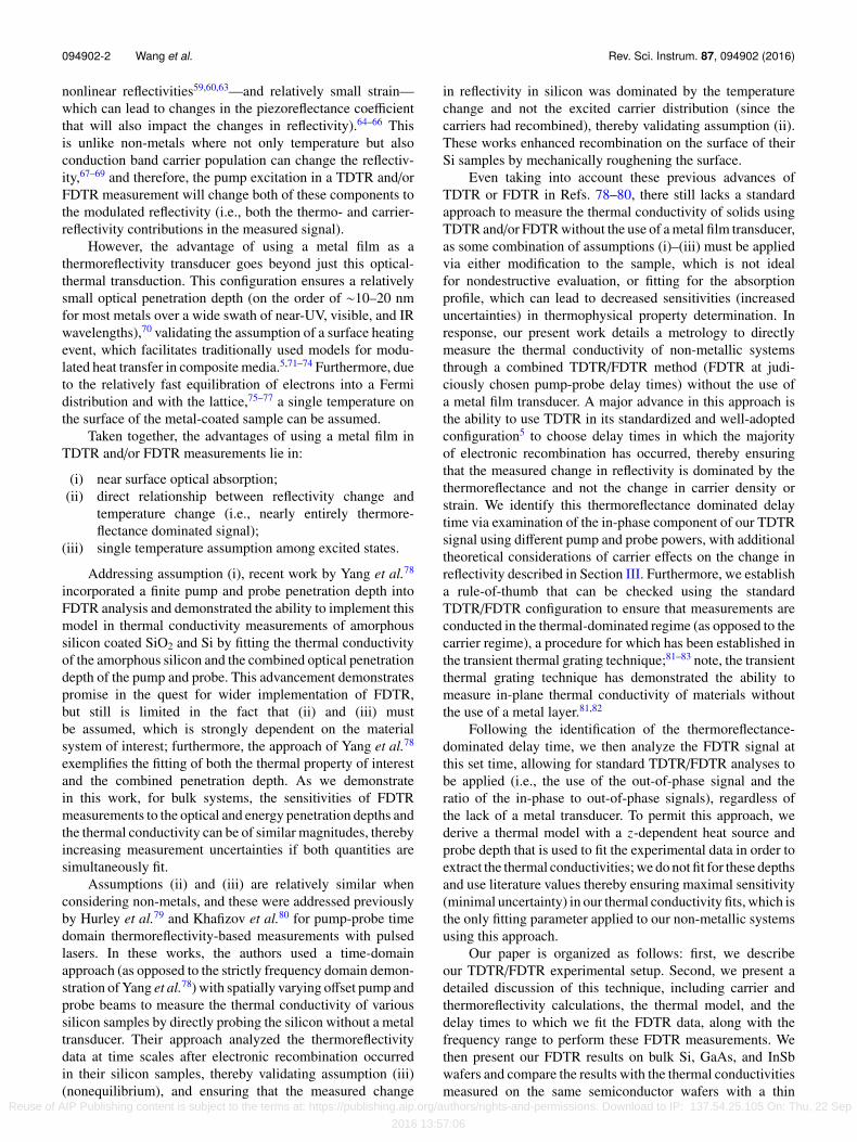
therefore converting the pump pulses to 400 nm. The probepulses are delayed up to 7 ns relative to the pump pulseswith a mechanical delay stage—in our current approach toTDTR/FDTR measurements without metal transducer, thisdelay is the first step used to assess the time after pumpexcitation in which the majority of the excited carriers haverelaxed, thereby ensuring the measured change in reflectivityis dominated by the thermoreflectivity component. To achievethese time delays, we use a doubling approach of the probepath on the delay stage as shown in Fig. 1, as opposed to thecommon approach of using multiple retroreflectors. A λ/2-wave plate is adjusted to ensure the probe beam is p-polarizedand gets fully transmitted through a polarizing beam splitter.
FIG. 1. A schematic showing the method of doubling the probe path overthe delay stage in our TDTR/FDTR setup. A λ/2 wave plate sends thep-polarized light into a polarizing beam splitter. Then a λ/4 wave plateconverts the linearly polarized light into circularly polarized light. The lightis reflected by a retro-reflector and then reaches a zero-degree mirror, whichreflects the light back along the same path. By adjusting the λ/4 wave plate,the reflected light can be converted into partially s-polarized, so that thiscomponent is reflected by the beam splitter.
A λ/4-wave plate is adjusted so that its fast axis is at 45 withprobe polarization to convert the linearly polarized light intocircularly polarized light. The probe is reflected by the retro-reflector to reach a zero-degree mirror, which reflects the lightback along the same path, doubling the distance traveled andthe resulting time delay. The circularly polarized probe is thenconverted to s-polarized light and is totally reflected by thepolarizing beam splitter after passing through the λ/4-waveplate. In practice, we find that sending the probe beam backalong its same incident path helps to minimize unintentionalmisalignment in the delay stage. A dichroic mirror is thenused to reflect the 400 nm pump light and transmit the 800 nmprobe light onto the sample. Both the pump and the probeare coaxially focused on the sample by an objective lens. Thechange in reflectivity of the probe off the sample surface,which is coaxially aligned with the pump, is monitored with abalanced amplified photodetector (Thorlabs PDB450A-AC),and the resulting converted voltage is directed to a lock-in-amplifier that is synced to the pump-modulation frequency. Wemonitor the in-phase (Vin) and out-of-phase (Vout) componentsof this lock-in signal.
III. DIRECT TDTR/FDTR PROBING PROCEDURE
A. Thermal and carrier effects
Photothermal reflectance signal generation in semicon-ductors can be understood in terms of the induced modulationof the refractive index. There are two mechanisms thatcontribute to the modulation of refractive index: the thermaleffect due to the local temperature change and the plasma effectdue to excited carrier density. Thus, the total photoreflectancesignal change can be expressed as the sum of these twocomponents86
∆R =∂R∂T∆T +
∂R∂N∆N, (1)
where ∂R/∂T is the temperature reflectance coefficient and∂R/∂N is the free-carrier reflectance coefficient. These twocoefficients of reflectance can be opposite in sign,69,86 resultingin a partial net cancellation of the observed signal. In orderto satisfy assumption (i) in nonmetals, an appropriate delaytime must be determined at which to perform FDTR such thatthe carrier contribution to the reflectance signal is negligiblecompared to the thermal contribution.
Several prior works have studied the variations inreflectivity caused by the relative contributions from thethermal and plasma effects. Previous works by the Mandelisgroup87,88 have discussed that the relative importance ofthe two mechanisms, which in the first approximation isdetermined by the ωτ product, where ω = 2π f is the angularmodulation frequency, and τ is the lifetime of the photoexcitedfree carriers. For ωτ ≪ 1, the change in reflectivity ismainly due to the local temperature rise since the excitedcarriers have decayed. Therefore, at low frequencies, thephotothermal reflectance signal has predominantly thermalorigins. In our work, the measurements on the samples withouta metal film transducer were carried out in the frequencyrange of 10 kHz–1 MHz, which is in the regime where
Reuse of AIP Publishing content is subject to the terms at: https://publishing.aip.org/authors/rights-and-permissions. Download to IP: 137.54.25.105 On: Thu, 22 Sep
2016 13:57:06
094902-4 Wang et al. Rev. Sci. Instrum. 87, 094902 (2016)
the thermal effects dominate the photothermal response andthe plasma contribution to the response is negligible in oursamples.
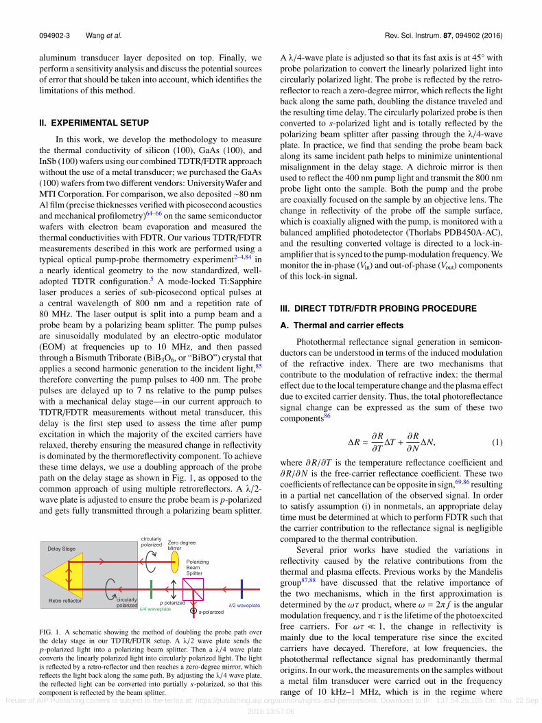
Furthermore, Guidotti and van Driel89 have shown thatthe photoexcited carriers thermalize to the lattice temperaturewithin a few picoseconds in Si; therefore, after relaxationof these photoexcited carriers in which a temperature canbe defined, any excess energy contributed by non-radiativelyrecombined phonons is thermalized into the Bose-Einsteindistribution during the time prescribed by our FDTR/TDTRmeasurements. Regardless, it is important to note that weconduct our measurements in the “low temperature perturba-tion” regime, so any deviation from equilibrium distributionsis assumed small, as we validate with various pump and probepowers, described in more detail in Section III D.
Another consideration when determining the delay timeis laser wavelength. Salnick and Opsal90 demonstrated therole of the pump and probe wavelengths on the thermal andplasma wave behavior, concluding that with a 400 nm (3.1 eV)pump and 800 nm (1.55 eV) probe (the wavelengths weapplied for our TDTR/FDTR measurements), thermal waveeffects are the primary mechanism affecting the change inreflectivity. Therefore, our proposed approach ensures thatour TDTR/FDTR measurements are always directly probingthe thermal transport (and not carrier transport) in our systemssince: (1) the modulation frequency that we employ duringour measurements ensures ωτ ≪ 1; (2) the pump and probewavelengths we use ensure the thermal wave effects aredominated in our measured reflectivity; and (3) the pump-probe delay time that we select to conduct our measurementsis a time that is greater than the carrier relaxation time.
While these aforementioned studies provide rough criteriafor minimizing carrier effects on reflectance, the choice oftime delay ultimately depends on material properties andpump/probe properties. Since the technique described hererelies on pulsed-pulsed (pump-probe) FDTR, we make use ofthe fact that pump pulses arriving at the sample are separatedtemporally by 12.5 ns. Thus, it is sufficient to study the timedomain solution to the coupled thermal and carrier responsesdescribed in Refs. 4 and 86. As such, we follow the approachoutlined by Tanaka et al. (Eqs. (14)–(18) in Ref. 69). Figure 2shows that for Si and GaAs, the carrier relaxation occurs onthe order of 10–100 ps such that reflectivity is dominatedby thermal response thereafter. The parameters used in thecalculations are listed in Table I. Moreover, a previous reportalso shows that the relaxation time for silicon is on the order of200 ps for similar experimental conditions as ours (includingpump and probe wavelengths).69 As such, in the followingexperiments, we performed the FDTR measurements at a timedelay of 5 ns, sufficiently long enough to avoid any carriereffects on reflectivity.
Finally, previous report by Johnson et al.81 shows thatthe carrier recombination time measured is on the order of1.7-10 ns for Si depending on the period spacings of thegratings in their work. They assert that since the ambipolarcarrier diffusion coefficient in Si is about an order of magnitudegreater than the thermal diffusivity, the electronic and thermalrelaxations are well separated in the time domain. In thiscontext, they use a biexponential fit to their experimental
FIG. 2. Thermal and carrier contributions to the measured reflectancechange during the pump-probe measurement. The calculations are based onEqs. (14)–(18) in Ref. 69.
data and characterize the faster transient decay as due tocarrier relaxation effects, which depends strongly on the carrierconcentrations. The longer decay is related to thermal effectsand most significantly the measured decay rates are shown tonot depend on the different pump energies and initial carrierconcentrations. Their findings along with other prior workssuggest that carrier dynamics in semiconductors are not anintrinsic property of the material but highly depend on extrinsicvariables such as laser fluence, photonic energy, and laserexcitation pulse-width, as we discussed above. Therefore,a direct “apples-to-apples” comparison between the carrierrelaxation rates in the work of Johnson et al.81 and thatreported in our work cannot be made; as we point out above,the calculated relaxation time in Si with the experimentalparameters in our work is <1 ns. However, in line withthe work of Johnson et al., we find that with the judiciouschoice of pump and probe powers, the FDTR signals atlonger time delays (5 ns) with varying powers are relativelyconstant (within experimental uncertainty, as described later
TABLE I. Parameters used in the calculations of Figure 2: γ3 is the Augerrecombination coefficient,91,92 DN is the ambipolar diffusion coefficient,93
S is the surface recombination velocity,67,94 Eg is the bandgap,95 DT is thethermal diffusivity,95 n is the complex refractive index,70 n1 is the real partof n,96 N is the carrier density,69 and T is temperature.
Parameter Silicon GaAs
γ3 (cm6/s) 7 × 10⁻³⁰ 4 × 10⁻³
DN (cm2/s) 20 10S (cm/s) 2.4 × 10⁵ 5 × 10⁵
Eg (eV) 1.1 1.43DT (cm2/s) 0.85 0.28n 5.57+0.39i 4.46+2.08i∂n1/∂N (cm3) −4.4×10⁻²² −4.4×10⁻²²
∂n1/∂T (K−1) 5.1 × 10⁻⁴ 2.0 × 10⁻⁴
Reuse of AIP Publishing content is subject to the terms at: https://publishing.aip.org/authors/rights-and-permissions. Download to IP: 137.54.25.105 On: Thu, 22 Sep
2016 13:57:06

094902-5 Wang et al. Rev. Sci. Instrum. 87, 094902 (2016)
in Section III D—cf., Fig. 5), even though the signals at shortertime delays (∼200 ps where carrier concentration effectsare dominant) demonstrate statistically significant differentsignals at varying pump energies. Therefore, using the sameprocedure as Johnson et al.,81 we support that at the time scalesand laser powers studied in this work, the reflectivity change inthe data presented in our manuscript is strictly in the thermallydominated regime and the carrier induced reflectivity changehas negligible effect.
B. Thermal model with finite optical penetration
The thermal model traditionally used for analyzing TDTRor pulsed FDTR data is based on solving the classical heatdiffusion equation while accounting for the pulse accumula-tion effect due to the high repetition rate of the laser.5,6,72,73,97
As previously discussed, usually, with a metal transducer, theoptical penetration depth of metals is very small (∼10 nm)and the heat source can be considered as a surface heat source.As outlined in Section I, Yang et al.78 have discussed thelimitations of using a surface heat source in this traditionallyassumed thermal diffusion model and utilized a convenientsimplification when the probe’s optical penetration depth isless than the heater penetration depth. In our case, we donot make this assumption regarding the relative pump andprobe penetration depths in our implementation for datafitting, as some of the semiconductors of interest exhibitoptical penetration depths that are comparable to the radiusof our pump and probe beams (e.g., in silicon, the opticalpenetration depth at 800 nm is ∼9.73 µm; note, the opticalpenetration depth is the inverse of the optical absorptioncoefficient).70 Therefore, we implement a generalized thermaldiffusion model applied in TDTR/FDTR analyses to includea z-dependent heat source and probe sampling depth. As aresult, the heat diffusion equation in cylindrical coordinates isgiven by
κrr
∂
∂r
(r∂T (z,r, t)
∂r
)+ κz
∂2T (z,r, t)∂z2
+1ς
S (r, t) exp(−zς
)= ρcp
∂T (z,r, t)∂t
, (2)
where κr and κz are the in-plane and cross-plane thermalconductivities, respectively, ρ is the mass density, cp is thespecific heat capacity (and the volumetric heat capacity isC = ρcp), and ς is the optical penetration depth of the pumpbeam; in the remainder of this work, we refer to ς as the heatpenetration depth to distinguish it from the optical penetrationdepth of the probe beam.98 We note that the heat penetrationdepth is the depth to which the laser energy is depositedinto the sample and is not the thermal penetration depth,which is related to the depth in which the modulated thermalwave extinguishes into the sample (the thermal penetrationdepth, which is modulation frequency dependent, is given byδthermal =
κ/πρcp f , where f is the modulation frequency of
the heat source). S (r, t) = 2πr2
0exp
(−2r2
r20
)g0(t) is the source
term resulting from the heat flux across the top surface,6
where r0 is the 1/e2 Gaussian pump beam radius and g0 (t)is a function of time that includes the power absorbed by the
sample at the pump wavelength. Taking the Fourier transformand Hankel transform of Eq. (2), we obtain
−κrk2T (z, k,ω) + κz∂2T (z, k,ω)
∂z2
+1ς
S (k,ω) exp(−zς
)= ρcpiωT (z, k,ω) , (3)
where ω is the angular frequency, k is the Hankel transformvariable, and T(z, k,ω) and S(k,ω) are the Fourier and Hankeltransform of T(z,r, t) and S(r, t), respectively. By solvingEq. (3) with an adiabatic boundary condition at the top surfaceand a semi-infinite boundary condition at the bottom surface,we can obtain the temperature profile function T(z, k,ω).
The reflectance change ∆R due to the heating eventscan be assumed to be linearly proportional to the surfacetemperature change: ∆R = βT (r , t), where β is the thermore-flectance coefficient, assuming this is the primary mechanismdriving the reflectivity change. Stated differently, the changein surface temperature is monitored by the change of thereflectance of the probe beam, assuming the modulatedreflectivity of the probe beam is driven by temperature. Thenthe reflected probe beam intensity, pr (r , t), can be expressed asweighting the incident probe beam intensity function throughthe temperature variation and integrating it over the filmthickness6,78,99
pr (r, t) =∞
0
pi (r, t) exp(−zδ
)βT (z,r, t) dz, (4)
where δ is the optical penetration depth of the probe. pi (r, t)= 2
πr21
exp(−2r2
r21
)g1(t),5 where r1 is the 1/e2 Gaussian probe
beam radius and g1(t) is a function of time that includes thepower in the probe beam. Finally, the frequency response ofpr (r , t), denoted as pr (r , ω), can be obtained by performinga Fourier transform Eq. (4). The pulse accumulation effect ofthe model is evoked in identical fashion as that outlined inRefs. 6 and 78.
In Figure 3, we show a representative TDTR/FDTRmeasurement of an intrinsic silicon (100) wafer that wasprobed directly with our system (i.e., no metal transducer),and the resultant fits with both a surface heat source modeland with z-dependent heat source model; for these analyses,we fit only the radial (in-plane) thermal conductivity ofthe silicon (κr), where all other inputs to the model areassumed constant (listed in the caption of Figure 3). Wenote that silicon is isotropic, so we expect κr = κz in thissystem. For relatively high thermal conductivity materials,this approach of TDTR/FDTR without the use of metaltransducer will consistently sample κr , as we discuss in detailin Section IV B. If the sample is isotropic, such as thosestudied in this work, then our measurement provides a uniquemetrology to measure κ = κr = κz and also provides a methodto measure the thermal conductivity of materials without thepotential for anisotropic failure of Fourier diffusion around themetal transducer/sample interface.100 In the situation wherethe material is anisotropic, our described implementationof TDTR/FDTR is most sensitive to in-plane transport for
Reuse of AIP Publishing content is subject to the terms at: https://publishing.aip.org/authors/rights-and-permissions. Download to IP: 137.54.25.105 On: Thu, 22 Sep
2016 13:57:06

094902-6 Wang et al. Rev. Sci. Instrum. 87, 094902 (2016)
FIG. 3. Model fits to TDTR/FDTR measurements of an intrinsic silicon(100) wafer without a metal transducer (henceforth referred to as “bare”)at a TDTR delay time of 5 ns. Fitting with z-dependent heat source(solid line) results in an in-plane thermal conductivity best fit value of κr= 149.8 ± 15.1 W m−1 K−1, while fitting with surface heat source (dashedline) results in poor goodness of fit for silicon. The parameters used infitting our model to the data are as follows: volumetric heat capacity of SiC = 1.63×10⁶ J m−3 K−1 (Ref. 95), pump beam radius= 11.3 µm, probebeam radius= 9.5 µm, optical penetration depth δ and heat penetration depthς are calculated with δ = λ/4πn2, where λ is 800 nm and 400 nm forprobe beam and pump beam, respectively, n2 is the extinction coefficient.From this, δ = 9.73 µm and ς = 97.90 nm.102 The uncertainty of the thermalconductivity value comes from ±5% variations of the pump and probe beamradii used in the fitting model.
relatively high κz systems, as discussed in more detail in oursensitivity analysis and limitations outlined in Section IV.
The data in Figure 3 were collected at a TDTR delay timeof 5 ns, and the selection of this time is discussed in detailin Sec. III C. The z-dependent heat source model providesa good fit to the experimental data and results in a best fitthermal conductivity of Si of κr = 149.8 ± 15.1 W m−1 K−1
(uncertainty comes from ±5% variations of pump and probebeam radii used in fitting the model to the data), consistentwith literature.101 Performing a fit with the model assuming asurface heat source results in a poor goodness of fit.
The results in this section demonstrate the ability toperform FDTR measurements at a specified TDTR delaytime (i.e., a hybrid TDTR/FDTR approach) without the useof a metal film transducer (henceforth, these samples arereferred to as “bare” to indicate the lack of metal coating).The intricacies and procedures to this approach are outlinedin Secs. III C and III D.
C. Fitting at different delay times
Our analysis relies on the fact that the measured change inmodulated reflectance is dominated by the thermoreflectancecomponent, as discussed in Section III A. Therefore, we selectdelay times in which to perform our FDTR measurementsthat ensure that the non-thermoreflectance contributions tothe modulated reflectivity signal are minimized. This is thesame principle that was used in previous TDTR79,80 andtransient grating procedures.81,83 However, unlike in theseworks, we posit that we can utilize the frequency domainresponse (i.e., FDTR) at these judiciously chosen time delays
in which the non-thermoreflectivity components to modulatedreflectance have been minimized, thereby generalizing ourapproach to any non-metal without the use of surfacemodification in a standardized TDTR geometry. Therefore, byperforming FDTR measurements at much longer delay timesand accounting for the out-of-phase response of the FDTRsignal, which, given low enough modulation frequencies,will be dominated by the heating of the pump, we canrelate the FDTR signal to the thermal diffusion equationoutlined in Sec. III B. This forms the basis of our hybridTDTR/FDTR approach. Hence, in practice, our approachis based on performing TDTR measurements at differentfrequencies.
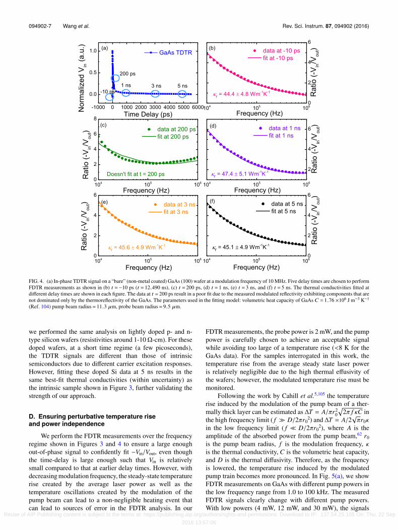
We show examples of this fitting approach for GaAs (100)wafers. Figure 4(a) shows the normalized in-phase componentof the lock-in amplifier signal (Vin) as a function of pump-probedelay time collected at a pump frequency of 10 MHz. Thechanges in this measured signal near time t = 0 ps correspondto the hot carrier dynamics from the absorption of the pumpbeam. After a few hundred picoseconds, this component ofthe signal relaxes, which corresponds to the extinction ofthe excited carrier portion of the reflectivity.103 While thethermoreflectivity component is also relaxing during this time,the carrier portion has been shown to relax more rapidly thanthe thermal portion. At ∼1 ns, the real component of thesignal is nearly fully relaxed, and the lock-in amplifier signalswill be dominated by the thermoreflectivity component ofthe modulated reflectivity measurements. Therefore, FDTRmeasurements should be performed at a delay time after thistime regime when the in-phase component is minimized.As typical with TDTR and FDTR analyses, after this time,we then analyze the ratio of the in-phase to out-of-phasesignal (−Vin/Vout), since the out-of-phase component is stillappreciable due to the thermomodulation component of thereflectivity, which is driven by the thermal properties of thesamples. Due to this, we perform FDTR measurements atrelatively low modulation frequencies to induce a larger out-of-phase signal; we discuss the implications of this selectionin more detail in Section IV.
Figures 4(b)–4(f) show the FDTR measurements of thesame GaAs wafer at delay times of −10 ps, 200 ps, 1 ns,3 ns, and 5 ns, respectively. The corresponding fitted thermalconductivities using the model discussed in Section III Aare listed in the plots; we note, again, that these thermalconductivities are κr , as we are insensitive to κz for GaAsover the frequency domain utilized in this work, as discussedin more detail in Section IV B. At all sampled delay times,except for t = 200 ps, the model fits the data well and resultsin best fits to the thermal conductivity that are consistentamong each other and with previous reports in the literature. At200 ps, the measured GaAs signal is not entirely dominatedby the thermoreflectivity component, rendering our thermaldiffusion model invalid to analyze the data. The monitoring ofthe in-phase component of the signal as a function of time todetermine when to fit −Vin/Vout in the FDTR analysis is key tothis approach. In the following discussions, we fit all FDTRdata at a delay time t = 5 ns.
To further validate our approach of analyzing the FDTRsignal at time-delays after the carrier reflectivity has relaxed,
Reuse of AIP Publishing content is subject to the terms at: https://publishing.aip.org/authors/rights-and-permissions. Download to IP: 137.54.25.105 On: Thu, 22 Sep
2016 13:57:06
094902-7 Wang et al. Rev. Sci. Instrum. 87, 094902 (2016)
FIG. 4. (a) In-phase TDTR signal on a “bare” (non-metal coated) GaAs (100) wafer at a modulation frequency of 10 MHz. Five delay times are chosen to performFDTR measurements as shown in (b) t =−10 ps (t = 12.490 ns), (c) t = 200 ps, (d) t = 1 ns, (e) t = 3 ns, and (f) t = 5 ns. The thermal conductivities fitted atdifferent delay times are shown in each figure. The data at t = 200 ps result in a poor fit due to the measured modulated reflectivity exhibiting components that arenot dominated only by the thermoreflectivity of the GaAs. The parameters used in the fitting model: volumetric heat capacity of GaAs C = 1.76 ×10⁶ J m−3 K−1
(Ref. 104) pump beam radius= 11.3 µm, probe beam radius= 9.5 µm.
we performed the same analysis on lightly doped p- and n-type silicon wafers (resistivities around 1-10Ω-cm). For thesedoped wafers, at a short time regime (a few picoseconds),the TDTR signals are different than those of intrinsicsemiconductors due to different carrier excitation responses.However, fitting these doped Si data at 5 ns results in thesame best-fit thermal conductivities (within uncertainty) asthe intrinsic sample shown in Figure 3, further validating thestrength of our approach.
D. Ensuring perturbative temperature riseand power independence
We perform the FDTR measurements over the frequencyregime shown in Figures 3 and 4 to ensure a large enoughout-of-phase signal to confidently fit −Vin/Vout, even thoughthe time-delay is large enough such that Vin is relativelysmall compared to that at earlier delay times. However, withdecreasing modulation frequency, the steady-state temperaturerise created by the average laser power as well as thetemperature oscillations created by the modulation of thepump beam can lead to a non-negligible heating event thatcan lead to sources of error in the FDTR analysis. In our
FDTR measurements, the probe power is 2 mW, and the pumppower is carefully chosen to achieve an acceptable signalwhile avoiding too large of a temperature rise (<8 K for theGaAs data). For the samples interrogated in this work, thetemperature rise from the average steady state laser poweris relatively negligible due to the high thermal effusivity ofthe wafers; however, the modulated temperature rise must bemonitored.
Following the work by Cahill et al.5,105 the temperaturerise induced by the modulation of the pump beam of a ther-mally thick layer can be estimated as ∆T = A/πr2
0
2π f κC in
the high frequency limit ( f ≫ D/2πr02) and ∆T = A/2
√πr0κ
in the low frequency limit ( f ≪ D/2πr02), where A is the
amplitude of the absorbed power from the pump beam,62 r0is the pump beam radius, f is the modulation frequency, κis the thermal conductivity, C is the volumetric heat capacity,and D is the thermal diffusivity. Therefore, as the frequencyis lowered, the temperature rise induced by the modulatedpump train becomes more pronounced. In Fig. 5(a), we showFDTR measurements on GaAs with different pump powers inthe low frequency range from 1.0 to 100 kHz. The measuredFDTR signals clearly change with different pump powers.With low powers (4 mW, 12 mW, and 30 mW), the signals
Reuse of AIP Publishing content is subject to the terms at: https://publishing.aip.org/authors/rights-and-permissions. Download to IP: 137.54.25.105 On: Thu, 22 Sep
2016 13:57:06

094902-8 Wang et al. Rev. Sci. Instrum. 87, 094902 (2016)
FIG. 5. (a) Experimental FDTR data of a bare GaAs (100) wafer measuredwith different pump powers. (b) Fitted thermal conductivities of GaAs waferby varying probe power with pump power of 10 mW. (c) Fitted thermalconductivities of GaAs wafer by varying pump power with probe power of4 mW.
diverge at low frequencies yet converge at high frequencies(>7 kHz), consistent with the discussion of non-perturbativeheating as frequency is lowered. So we performed FDTRmeasurements with frequency range starting from 10 kHz.For the data collected at the highest power shown in thisfigure (50 mW), the shape of the signal changes substantiallyand cannot be fit with our thermal model, indicating thatthe average temperature oscillations are too high to assumea relatively constant temperature over the entire frequencyrange, in addition to other potential factors that are notaccounted for in our linear perturbation thermal analysis,such as increased carrier lifetimes that would lead to the ωτproduct not ≪1. From this, we assert that when collectingFDTR data, several powers should be used to ensure thatthe fitted data lie in a regime of a relatively small andlinear temperature perturbation. This can also be checked bycomparing the normalized in-phase response as a functionof time. The importance of pump power in measuring theFDTR in the linear perturbation thermoreflectance-dominatedresponse regime is also exemplified in our previous discussionregarding the carrier dynamics (Section III A). Figures 5(b)and 5(c) show the measured thermal conductivities of GaAsat various pump and probe powers. As shown in these figures,within uncertainties, the measured thermal conductivities donot show a dependence on the pump and probe powers.
This check should be performed to ensure that the data arecollected in a regime where the thermal signal dominatesthe measured reflectivity (negligible carrier component);note, this procedure is consistent with the similar checkused in the transient grating experiments described byJohnson et al.81
IV. DATA ANALYSIS AND SENSITIVITIES
A. FDTR data and calibration with and withouta metal transducer
We demonstrate the applicability of this approach byperforming this TDTR/FDTR procedure on both bare intrinsicSi (100), GaAs (100) (from MTI corporation and University-Wafer), and InSb (100) wafers along with a portion of the samewafers coated with ∼80 nm of Al (a more traditional FDTRapproach), as shown in Fig. 6. The only difference betweenthese two measurements shown in each plot is the aluminummetal transducer layer. The measurements were performedover a frequency range of 10 kHz–1 MHz at a delay time of5 ns. Fitting was performed using a nonlinear least-squaresminimization routine. The spot radii used in the fitting were11.3 µm for the pump beam and 9.5 µm for the probe beam,which were calibrated with FDTR measurements, as discussedin more detail in Section IV B. We assumed literaturevalues for the volumetric heat capacity C for Si (C = 1.63× 10⁶ J m−3 K−1),95 GaAs (C = 1.76 × 10⁶ J m−3 K−1),104 andInSb (C = 1.15 × 10⁶ J m−3 K−1).106 The optical penetrationdepths for each sample δ were calculated as δ = λ/4πn2,where λ is 400 nm and 800 nm for pump beam and probebeam, respectively, n2 is the extinction coefficient. We assumethat the optical penetration depth of the pump is equivalent tothe heat penetration depth, ς.78
We find that only Si needs to be fitted with a z-dependentheat source model due to the large optical penetration depthof the probe compared to the heat penetration depth (δSi= 9.73 µm, ςSi = 97.90 nm).102 For GaAs and InSb, the opticalpenetration depths are smaller and the heat penetration depthsare near surface and metal like at 400 nm (δGaAs = 0.74 µm,ςGaAs = 14.84 nm, δInSb = 91.26 nm, ςInSb = 15.79 nm),102
and in this limit, a surface heat source can be assumed inthe solution to the diffusion equation (similar to a traditionalFDTR/TDTR analysis with a metal film transducer). Asan example, take GaAs; the fitted thermal conductivityof GaAs (100) wafer from MTI corporation is κr = 45.1± 4.9 W m−1 K−1 when using surface heat source model,and κr = 45.0 ± 4.7 W m−1 K−1 when using z-dependent heatsource model. As a result, the surface heat source solution canbe assumed for fitting the data of GaAs and InSb. The freeparameter in all measurements on the bare samples is only thethermal conductivity of the sample. For samples with the Altransducer layer, the Al/semiconductor interface conductancesused as input parameters in the FDTR fits are measured withTDTR at 10 MHz.
Figure 6 shows experimental data and the best-fit curves.The fitted thermal conductivities for each sample are shown ineach figure. As shown in figure, the thermal conductivitiesmeasured with the Al layer and direct FDTR probing
Reuse of AIP Publishing content is subject to the terms at: https://publishing.aip.org/authors/rights-and-permissions. Download to IP: 137.54.25.105 On: Thu, 22 Sep
2016 13:57:06

094902-9 Wang et al. Rev. Sci. Instrum. 87, 094902 (2016)
FIG. 6. Data points (symbols) and best fit curves (solid lines) for the FDTR measurements on (a) intrinsic Si (100), (b) GaAs (100) (MTI), (c) GaAs (100)(University Wafer), and (d) InSb (100). The FDTR measurements of the same wafers with 80 nm Al layers are also shown in figure. The fitted thermalconductivities are shown for each case. The FDTR measurements are performed in a frequency range of 10 kHz–1 MHz and at a delay time of 5 ns. For sampleswith Al layer, the Al/semiconductor interface conductance h used in FDTR fits is measured with TDTR method at 10 MHz: hAl/Si= 2.0×10⁸ W m−2 K−1,hAl/GaAs= 8.5×10⁷ W m−2 K−1, and hAl/InSb= 5.1×10⁷ W m−2 K−1.
agree within experimental uncertainty, indicating the potentialfor this procedure to measure the thermal conductivity ofmaterials without a metal transducer.
B. Sensitivity analysis and sources of error
To quantify the sensitivity of the various experimentalparameters in this direct probing TDTR/FDTR method, we usethe approach by Costescu et al.,107 where the sensitivity of theratio to a parameter x is defined by Sx = ∂(−Vin/Vout)/∂ ln(x).We calculated the sensitivities for the in-plane thermalconductivity, cross-plane thermal conductivity, and spot size.For Si, since we applied the z-dependent heat source model, wealso show the sensitivity analysis of optical penetration depthand heat penetration depth. The results are shown in Fig. 7for (a) InSb, (b) GaAs, and (c) Si. The sensitivity analysis isperformed over a frequency range of 1 kHz–10 MHz with adelay time of 5 ns. Clearly, direct FDTR probing is sensitiveto the in-plane thermal conductivity while insensitive to thecross-plane thermal conductivity, since there is no significanttemperature gradient in the cross-plane direction comparedto the in-plane direction at these heat penetration depths andmodulation frequencies. As a result, this technique can be used
to measure in-plane thermal conductivities. Although for theisotropic samples interrogated in this work, the in- and cross-plane thermal conductivities can be assumed identical, foranisotropic samples or layered structures, our approach couldpresent a method to measure the in-plane thermal conductivity.We do not pursue this approach in our current work but offerthis as a potential future direction.
We also note that the samples examined in this workhave relatively high thermal conductivities when comparedto glassy/disordered or nanostructured samples designedto minimize phonon thermal transport. For relatively lowthermal conductivity samples, the heating induced by thepump power could lead to non-negligible heating, renderingour assumption of a relatively constant temperature invalid.While in principle this heating could be accounted for viamore sophisticated analyses, it is beyond the scope of thispresent work. However, as the thermal conductivity of thesample is reduced, the temperature gradients in the cross-planedirection become more pronounced, and if the penetrationdepths are relatively shallow, this approach can be appliedto measure the cross-plane thermal conductivity. Again, weleave this as a potential future direction of this TDTR/FDTRprocedure.
Reuse of AIP Publishing content is subject to the terms at: https://publishing.aip.org/authors/rights-and-permissions. Download to IP: 137.54.25.105 On: Thu, 22 Sep
2016 13:57:06

094902-10 Wang et al. Rev. Sci. Instrum. 87, 094902 (2016)
FIG. 7. FDTR measurement sensitivity of the ratio (−Vin/Vout) to the in-plane thermal conductivities, cross-plane thermal conductivities, and the laserspot size for (a) InSb, (b) GaAs, and (c) Si. Since the fitting model used for Siincludes the z-dependent heat source, the sensitivities to the heat penetrationdepth and optical penetration depth are included.
As apparent from Fig. 7, direct FDTR probing is verysensitive to the spot size and optical penetration depth. In fact,for the Si, the penetration depths offer very similar sensitivities(opposite and similar magnitudes) to the thermal conductivity.In the fitting of our model to the data, we assumed literaturevalues for the penetration depths, as fitting of this quantitycan substantially increase the measurement uncertainty indetermining the thermal conductivity. As we do not treat thepenetration depths as free parameters, the main source of errorin our technique is in the spot size.
In Fig. 8, we plot the best-fit curves for Si (fit curveshown in Fig. 6(a)), and also the curves by varying thethermal conductivity κr ± 10% (Fig. 8(a)), pump and probebeam spot sizes ±5% (Fig. 8(b)), and optical penetrationdepth δ ± 10% (Fig. 8(c)). We can see 10% variation in δnegligibly affects the best fit thermal conductivities; however,the fitting curves of 5% variations in spot size are almost thesame as those of 10% variations in thermal conductivity. As aresult, 5% variation in spot size will cause around 10% errorin the thermal conductivity measurements. To obtain accuratethermal conductivity values with direct FDTR probing, precisespot sizes are crucial.
We calibrated the spot sizes by performing FDTRmeasurements at a time delay of 5 ns on a SiO2 substratecoated with 80 nm Al layer and fit the effective spot size withthe data. FDTR measurements performed at this time delayare most sensitive to the effective pump and probe spot sizesassuming the metal film thickness is well known (which we
FIG. 8. Best-fit curve for Si and curves varied by (a) thermal conductivityκ±10%, (b) spot size ±5%, and (c) optical penetration depth δ±10%. 5%variations in spot size cause nearly 10% off in thermal conductivities. Allplots are at a time delay of 5 ns.
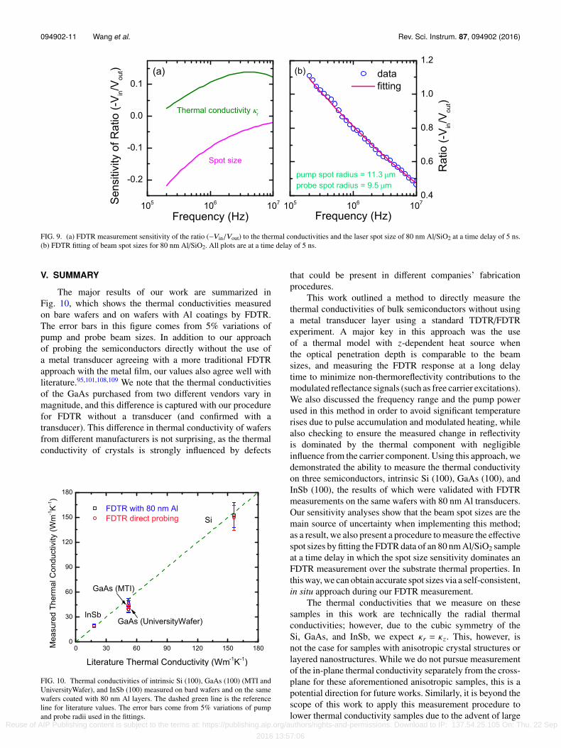
measure with profilometry and picosecond acoustics usingTDTR at the same measurement location). In Fig. 9(a), weshow the sensitivity of the solution to the spot size, and forreference, substrate thermal conductivity at this time delay.Over this frequency range (200 kHz–10 MHz), the sensitivityof an FDTR measurement to the spot size dominates thatof the thermal conductivity. As a result, we fit the effectivespot size
r2
0 + r21 from the FDTR measurements in this
frequency range as shown in Fig. 9(b), where r0 and r1are the pump and probe radii, respectively. The fitted radiiresult in 13.6 µm for the pump beam spot and 5.5 µmfor the probe beam spot. For comparison, the measuredpump and probe radii with the knife-edge technique are 14.0(± 0.5) µm and 5.5 (± 0.5) µm, respectively. The difficulty ininterpreting these measurements originates from the fact thatthere is high uncertainty in precisely knowing the positionof the exact sample plane at focus (during the TDTR/FDTRmeasurements) and that in the knife-edge. In this regard,the highest accuracy in precisely determining the spot sizeat the sample focus in our TDTR/FDTR measurements iswith the method by using FDTR measurements at relativelylow frequencies where the thermal model is highly sensitiveto the effective spot size. Therefore, we assert that thismethod of using FDTR at long time delays when themeasurement sensitivity to the spot size is relatively largeprovides a unique method to determine the spot sizes duringthermoreflectance techniques via a self-consistent and in situapproach.
Reuse of AIP Publishing content is subject to the terms at: https://publishing.aip.org/authors/rights-and-permissions. Download to IP: 137.54.25.105 On: Thu, 22 Sep
2016 13:57:06
094902-11 Wang et al. Rev. Sci. Instrum. 87, 094902 (2016)
FIG. 9. (a) FDTR measurement sensitivity of the ratio (−Vin/Vout) to the thermal conductivities and the laser spot size of 80 nm Al/SiO2 at a time delay of 5 ns.(b) FDTR fitting of beam spot sizes for 80 nm Al/SiO2. All plots are at a time delay of 5 ns.
V. SUMMARY
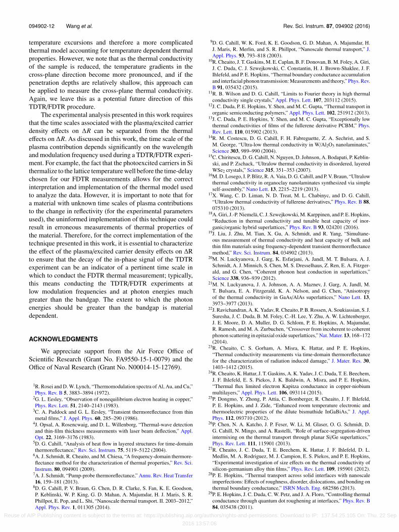
The major results of our work are summarized inFig. 10, which shows the thermal conductivities measuredon bare wafers and on wafers with Al coatings by FDTR.The error bars in this figure comes from 5% variations ofpump and probe beam sizes. In addition to our approachof probing the semiconductors directly without the use ofa metal transducer agreeing with a more traditional FDTRapproach with the metal film, our values also agree well withliterature.95,101,108,109 We note that the thermal conductivitiesof the GaAs purchased from two different vendors vary inmagnitude, and this difference is captured with our procedurefor FDTR without a transducer (and confirmed with atransducer). This difference in thermal conductivity of wafersfrom different manufacturers is not surprising, as the thermalconductivity of crystals is strongly influenced by defects
FIG. 10. Thermal conductivities of intrinsic Si (100), GaAs (100) (MTI andUniversityWafer), and InSb (100) measured on bard wafers and on the samewafers coated with 80 nm Al layers. The dashed green line is the referenceline for literature values. The error bars come from 5% variations of pumpand probe radii used in the fittings.
that could be present in different companies’ fabricationprocedures.
This work outlined a method to directly measure thethermal conductivities of bulk semiconductors without usinga metal transducer layer using a standard TDTR/FDTRexperiment. A major key in this approach was the useof a thermal model with z-dependent heat source whenthe optical penetration depth is comparable to the beamsizes, and measuring the FDTR response at a long delaytime to minimize non-thermoreflectivity contributions to themodulated reflectance signals (such as free carrier excitations).We also discussed the frequency range and the pump powerused in this method in order to avoid significant temperaturerises due to pulse accumulation and modulated heating, whilealso checking to ensure the measured change in reflectivityis dominated by the thermal component with negligibleinfluence from the carrier component. Using this approach, wedemonstrated the ability to measure the thermal conductivityon three semiconductors, intrinsic Si (100), GaAs (100), andInSb (100), the results of which were validated with FDTRmeasurements on the same wafers with 80 nm Al transducers.Our sensitivity analyses show that the beam spot sizes are themain source of uncertainty when implementing this method;as a result, we also present a procedure to measure the effectivespot sizes by fitting the FDTR data of an 80 nm Al/SiO2 sampleat a time delay in which the spot size sensitivity dominates anFDTR measurement over the substrate thermal properties. Inthis way, we can obtain accurate spot sizes via a self-consistent,in situ approach during our FDTR measurement.
The thermal conductivities that we measure on thesesamples in this work are technically the radial thermalconductivities; however, due to the cubic symmetry of theSi, GaAs, and InSb, we expect κr = κz. This, however, isnot the case for samples with anisotropic crystal structures orlayered nanostructures. While we do not pursue measurementof the in-plane thermal conductivity separately from the cross-plane for these aforementioned anisotropic samples, this is apotential direction for future works. Similarly, it is beyond thescope of this work to apply this measurement procedure tolower thermal conductivity samples due to the advent of large
Reuse of AIP Publishing content is subject to the terms at: https://publishing.aip.org/authors/rights-and-permissions. Download to IP: 137.54.25.105 On: Thu, 22 Sep
2016 13:57:06
094902-12 Wang et al. Rev. Sci. Instrum. 87, 094902 (2016)
temperature excursions and therefore a more complicatedthermal model accounting for temperature dependent thermalproperties. However, we note that as the thermal conductivityof the sample is reduced, the temperature gradients in thecross-plane direction become more pronounced, and if thepenetration depths are relatively shallow, this approach canbe applied to measure the cross-plane thermal conductivity.Again, we leave this as a potential future direction of thisTDTR/FDTR procedure.
The experimental analysis presented in this work requiresthat the time scales associated with the plasma/excited carrierdensity effects on ∆R can be separated from the thermaleffects on ∆R. As discussed in this work, the time scale of theplasma contribution depends significantly on the wavelengthand modulation frequency used during a TDTR/FDTR experi-ment. For example, the fact that the photoexcited carriers in Sithermalize to the lattice temperature well before the time-delaychosen for our FDTR measurements allows for the correctinterpretation and implementation of the thermal model usedto analyze the data. However, it is important to note that fora material with unknown time scales of plasma contributionsto the change in reflectivity (for the experimental parametersused), the uninformed implementation of this technique couldresult in erroneous measurements of thermal properties ofthe material. Therefore, for the correct implementation of thetechnique presented in this work, it is essential to characterizethe effect of the plasma/excited carrier density effects on ∆Rto ensure that the decay of the in-phase signal of the TDTRexperiment can be an indicator of a pertinent time scale inwhich to conduct the FDTR thermal measurement; typically,this means conducting the TDTR/FDTR experiments atlow modulation frequencies and at photon energies muchgreater than the bandgap. The extent to which the photonenergies should be greater than the bandgap is materialdependent.
ACKNOWLEDGMENTS
We appreciate support from the Air Force Office ofScientific Research (Grant No. FA9550-15-1-0079) and theOffice of Naval Research (Grant No. N00014-15-12769).
1R. Rosei and D. W. Lynch, “Thermomodulation spectra of Al, Au, and Cu,”Phys. Rev. B 5, 3883–3894 (1972).
2G. L. Eesley, “Observation of nonequilibrium electron heating in copper,”Phys. Rev. Lett. 51, 2140–2143 (1983).
3C. A. Paddock and G. L. Eesley, “Transient thermoreflectance from thinmetal films,” J. Appl. Phys. 60, 285–290 (1986).
4J. Opsal, A. Rosencwaig, and D. L. Willenborg, “Thermal-wave detectionand thin-film thickness measurements with laser beam deflection,” Appl.Opt. 22, 3169–3176 (1983).
5D. G. Cahill, “Analysis of heat flow in layered structures for time-domainthermoreflectance,” Rev. Sci. Instrum. 75, 5119–5122 (2004).
6A. J. Schmidt, R. Cheaito, and M. Chiesa, “A frequency-domain thermore-flectance method for the characterization of thermal properties,” Rev. Sci.Instrum. 80, 094901 (2009).
7A. J. Schmidt, “Pump-probe thermoreflectance,” Annu. Rev. Heat Transfer16, 159–181 (2013).
8D. G. Cahill, P. V. Braun, G. Chen, D. R. Clarke, S. Fan, K. E. Goodson,P. Keblinski, W. P. King, G. D. Mahan, A. Majumdar, H. J. Maris, S. R.Phillpot, E. Pop, and L. Shi, “Nanoscale thermal transport. II. 2003–2012,”Appl. Phys. Rev. 1, 011305 (2014).
9D. G. Cahill, W. K. Ford, K. E. Goodson, G. D. Mahan, A. Majumdar, H.J. Maris, R. Merlin, and S. R. Phillpot, “Nanoscale thermal transport,” J.Appl. Phys. 93, 793–818 (2003).
10R. Cheaito, J. T. Gaskins, M. E. Caplan, B. F. Donovan, B. M. Foley, A. Giri,J. C. Duda, C. J. Szwejkowski, C. Constantin, H. J. Brown-Shaklee, J. F.Ihlefeld, and P. E. Hopkins, “Thermal boundary conductance accumulationand interfacial phonon transmission: Measurements and theory,” Phys. Rev.B 91, 035432 (2015).
11R. B. Wilson and D. G. Cahill, “Limits to Fourier theory in high thermalconductivity single crystals,” Appl. Phys. Lett. 107, 203112 (2015).
12J. C. Duda, P. E. Hopkins, Y. Shen, and M. C. Gupta, “Thermal transport inorganic semiconducting polymers,” Appl. Phys. Lett. 102, 251912 (2013).
13J. C. Duda, P. E. Hopkins, Y. Shen, and M. C. Gupta, “Exceptionally lowthermal conductivities of films of the fullerene derivative PCBM,” Phys.Rev. Lett. 110, 015902 (2013).
14R. M. Costescu, D. G. Cahill, F. H. Fabreguette, Z. A. Sechrist, and S.M. George, “Ultra-low thermal conductivity in W/Al2O3 nanolaminates,”Science 303, 989–990 (2004).
15C. Chiritescu, D. G. Cahill, N. Nguyen, D. Johnson, A. Bodapati, P. Keblin-ski, and P. Zschack, “Ultralow thermal conductivity in disordered, layeredWSe2 crystals,” Science 315, 351–353 (2007).
16M. D. Losego, I. P. Blitz, R. A. Vaia, D. G. Cahill, and P. V. Braun, “Ultralowthermal conductivity in organoclay nanolaminates synthesized via simpleself-assembly,” Nano Lett. 13, 2215–2219 (2013).
17X. Wang, C. D. Liman, N. D. Treat, M. L. Chabinyc, and D. G. Cahill,“Ultralow thermal conductivity of fullerene derivatives,” Phys. Rev. B 88,075310 (2013).
18A. Giri, J.-P. Niemelä, C. J. Szwejkowski, M. Karppinen, and P. E. Hopkins,“Reduction in thermal conductivity and tunable heat capacity of inor-ganic/organic hybrid superlattices,” Phys. Rev. B 93, 024201 (2016).
19J. Liu, J. Zhu, M. Tian, X. Gu, A. Schmidt, and R. Yang, “Simultane-ous measurement of thermal conductivity and heat capacity of bulk andthin film materials using frequency-dependent transient thermoreflectancemethod,” Rev. Sci. Instrum. 84, 034902 (2013).
20M. N. Luckyanova, J. Garg, K. Esfarjani, A. Jandl, M. T. Bulsara, A. J.Schmidt, A. J. Minnich, S. Chen, M. S. Dresselhaus, Z. Ren, E. A. Fitzger-ald, and G. Chen, “Coherent phonon heat conduction in superlattices,”Science 338, 936–939 (2012).
21M. N. Luckyanova, J. A. Johnson, A. A. Maznev, J. Garg, A. Jandl, M.T. Bulsara, E. A. Fitzgerald, K. A. Nelson, and G. Chen, “Anisotropyof the thermal conductivity in GaAs/AlAs superlattices,” Nano Lett. 13,3973–3977 (2013).
22J. Ravichandran, A. K. Yadav, R. Cheaito, P. B. Rossen, A. Soukiassian, S. J.Suresha, J. C. Duda, B. M. Foley, C.-H. Lee, Y. Zhu, A. W. Lichtenberger,J. E. Moore, D. A. Muller, D. G. Schlom, P. E. Hopkins, A. Majumdar,R. Ramesh, and M. A. Zurbuchen, “Crossover from incoherent to coherentphonon scattering in epitaxial oxide superlattices,” Nat. Mater. 13, 168–172(2014).
23R. Cheaito, C. S. Gorham, A. Misra, K. Hattar, and P. E. Hopkins,“Thermal conductivity measurements via time-domain thermoreflectancefor the characterization of radiation induced damage,” J. Mater. Res. 30,1403–1412 (2015).
24R. Cheaito, K. Hattar, J. T. Gaskins, A. K. Yadav, J. C. Duda, T. E. Beechem,J. F. Ihlefeld, E. S. Piekos, J. K. Baldwin, A. Misra, and P. E. Hopkins,“Thermal flux limited electron Kapitza conductance in copper-niobiummultilayers,” Appl. Phys. Lett. 106, 093114 (2015).
25P. Dongmo, Y. Zhong, P. Attia, C. Bomberger, R. Cheaito, J. F. Ihlefeld,P. E. Hopkins, and J. Zide, “Enhanced room temperature electronic andthermoelectric properties of the dilute bismuthide InGaBiAs,” J. Appl.Phys. 112, 093710 (2012).
26P. Chen, N. A. Katcho, J. P. Feser, W. Li, M. Glaser, O. G. Schmidt, D.G. Cahill, N. Mingo, and A. Rastelli, “Role of surface-segregation-drivenintermixing on the thermal transport through planar Si/Ge superlattices,”Phys. Rev. Lett. 111, 115901 (2013).
27R. Cheaito, J. C. Duda, T. E. Beechem, K. Hattar, J. F. Ihlefeld, D. L.Medlin, M. A. Rodriguez, M. J. Campion, E. S. Piekos, and P. E. Hopkins,“Experimental investigation of size effects on the thermal conductivity ofsilicon-germanium alloy thin films,” Phys. Rev. Lett. 109, 195901 (2012).
28P. E. Hopkins, “Thermal transport across solid interfaces with nanoscaleimperfections: Effects of roughness, disorder, dislocations, and bonding onthermal boundary conductance,” ISRN Mech. Eng. 682586 (2013).
29P. E. Hopkins, J. C. Duda, C. W. Petz, and J. A. Floro, “Controlling thermalconductance through quantum dot roughening at interfaces,” Phys. Rev. B84, 035438 (2011).
Reuse of AIP Publishing content is subject to the terms at: https://publishing.aip.org/authors/rights-and-permissions. Download to IP: 137.54.25.105 On: Thu, 22 Sep
2016 13:57:06

094902-13 Wang et al. Rev. Sci. Instrum. 87, 094902 (2016)
30J. C. Duda and P. E. Hopkins, “Systematically controlling Kapitza conduc-tance via chemical etching,” Appl. Phys. Lett. 100, 111602 (2012).
31P. E. Hopkins, L. M. Phinney, J. R. Serrano, and T. E. Beechem, “Effectsof surface roughness and oxide layer on the thermal boundary conductanceat aluminum/silicon interfaces,” Phys. Rev. B 82, 085307 (2010).
32P. E. Hopkins and P. M. Norris, “Thermal boundary conductance responseto a change in Cr/Si interfacial properties,” Appl. Phys. Lett. 89, 131909(2006).
33P. E. Hopkins, P. M. Norris, R. J. Stevens, T. Beechem, and S. Graham,“Influence of interfacial mixing on thermal boundary conductance acrossa chromium/silicon interface,” J. Heat Transfer 130, 062402 (2008).
34P. E. Hopkins, J. C. Duda, S. P. Clark, C. P. Hains, T. J. Rotter, L. M. Phinney,and G. Balakrishnan, “Effect of dislocation density on thermal boundaryconductance across GaSb/GaAs interfaces,” Appl. Phys. Lett. 98, 161913(2011).
35Z. Su, J. P. Freedman, J. H. Leach, E. A. Preble, R. F. Davis, and J. A.Malen, “The impact of film thickness and substrate surface roughness onthe thermal resistance of aluminum nitride nucleation layers,” J. Appl.Phys. 113, 213502 (2013).
36Z. Su, L. Huang, F. Liu, J. P. Freedman, L. M. Porter, R. F. Davis, and J.A. Malen, “Layer-by-layer thermal conductivities of the Group III nitridefilms in blue/green light emitting diodes,” Appl. Phys. Lett. 100, 201106(2012).
37J. P. Freedman, X. Yu, R. F. Davis, A. J. Gellman, and J. A. Malen, “Thermalinterface conductance across metal alloy-dielectric interfaces,” Phys. Rev.B 93, 035309 (2016).
38B. M. Foley, S. C. Hernández, J. C. Duda, J. T. Robinson, S. G. Walton, andP. E. Hopkins, “Modifying surface energy of graphene via plasma-basedchemical functionalization to tune thermal and electrical transport at metalinterfaces,” Nano Lett. 15, 4876–4882 (2015).
39P. E. Hopkins, M. Baraket, E. V. Barnat, T. E. Beechem, S. P. Kearney,J. C. Duda, J. T. Robinson, and S. G. Walton, “Manipulating thermalconductance at metal-graphene contacts via chemical functionalization,”Nano Lett. 12, 590–595 (2012).
40M. D. Losego, M. E. Grady, N. R. Sottos, D. G. Cahill, and P. V. Braun,“Effects of chemical bonding on heat transport across interfaces,” Nat.Mater. 11, 502–506 (2012).
41J. Yang, E. Ziade, C. Maragliano, R. Crowder, X. Wang, M. Stefancich, M.Chiesa, A. K. Swan, and A. J. Schmidt, “Thermal conductance imaging ofgraphene contacts,” J. Appl. Phys. 116, 023515 (2014).
42S. Majumdar, J. A. Sierra-Suarez, S. N. Schiffres, W.-L. Ong, C. F. Higgs,A. J. H. McGaughey, and J. A. Malen, “Vibrational mismatch of metal leadscontrols thermal conductance of self-assembled monolayer junctions,”Nano Lett. 15, 2985–2991 (2015).
43Z. Ge, D. G. Cahill, and P. V. Braun, “Thermal conductance of hydrophilicand hydrophobic interfaces,” Phys. Rev. Lett. 96, 186101 (2006).
44Z. Tian, A. Marconnet, and G. Chen, “Enhancing solid-liquid interfacethermal transport using self-assembled monolayers,” Appl. Phys. Lett. 106,211602 (2015).
45H. Harikrishna, W. A. Ducker, and S. T. Huxtable, “The influence ofinterface bonding on thermal transport through solid–liquid interfaces,”Appl. Phys. Lett. 102, 251606 (2013).
46J. Park, J. Huang, W. Wang, C. J. Murphy, and D. G. Cahill, “Heat transportbetween Au nanorods, surrounding liquids, and solid supports,” J. Phys.Chem. C 116, 26335–26341 (2012).
47K. T. Regner, J. P. Freedman, and J. A. Malen, “Advances in studyingphonon mean free path dependent contributions to thermal conductivity,”Nanoscale Microscale Thermophys. Eng. 19, 183–205 (2015).
48K. T. Regner, S. Majumdar, and J. A. Malen, “Instrumentation of broadbandfrequency domain thermoreflectance for measuring thermal conductivityaccumulation functions,” Rev. Sci. Instrum. 84, 064901 (2013).
49K. T. Regner, D. P. Sellan, Z. Su, C. H. Amon, A. J. H. McGaughey, andJ. A. Malen, “Broadband phonon mean free path contributions to thermalconductivity measured using frequency domain thermoreflectance,” Nat.Commun. 4, 1640 (2013).
50K. T. Regner, L. C. Wei, and J. A. Malen, “Interpretation of thermore-flectance measurements with a two-temperature model including non-surface heat deposition,” J. Appl. Phys. 118, 235101 (2015).
51J. P. Freedman, J. H. Leach, E. A. Preble, Z. Sitar, R. F. Davis, and J. A.Malen, “Universal phonon mean free path spectra in crystalline semicon-ductors at high temperature,” Sci. Rep. 3, 2963 (2013).
52A. J. Minnich, J. A. Johnson, A. J. Schmidt, K. Esfarjani, M. S. Dresselhaus,K. A. Nelson, and G. Chen, “Thermal conductivity spectroscopy techniqueto measure phonon mean free paths,” Phys. Rev. Lett. 107, 095901 (2011).
53K. M. Hoogeboom-Pot, J. N. Hernandez-Charpak, X. Gu, T. D. Frazer,E. H. Anderson, W. Chao, R. W. Falcone, R. Yang, M. M. Murnane, H.C. Kapteyn, and D. Nardi, “A new regime of nanoscale thermal transport:Collective diffusion increases dissipation efficiency,” Proc. Natl. Acad. Sci.U. S. A. 112, 4846–4851 (2015).
54M. E. Siemens, Q. Li, R. Yang, K. A. Nelson, E. H. Anderson, M. M. Mur-nane, and H. C. Kapteyn, “Quasi-ballistic thermal transport from nanoscaleinterfaces observed using ultrafast coherent soft X-ray beams,” Nat. Mater.9, 26–30 (2010).
55L. Zeng, K. C. Collins, Y. Hu, M. N. Luckyanova, A. A. Maznev, S.Huberman, V. Chiloyan, J. Zhou, X. Huang, K. A. Nelson, and G. Chen,“Measuring phonon mean free path distributions by probing quasiballisticphonon transport in grating nanostructures,” Sci. Rep. 5, 17131 (2015).
56J. Yang, C. Maragliano, and A. J. Schmidt, “Thermal property microscopywith frequency domain thermoreflectance,” Rev. Sci. Instrum. 84, 104904(2013).
57X. Zheng, D. G. Cahill, R. Krasnochtchekov, R. S. Averback, and J.-C. Zhao, “High-throughput thermal conductivity measurements of nickelsolid solutions and the applicability of the Wiedemann-Franz law,” ActaMater. 55, 5177–5185 (2007).
58E. Lopez-Honorato, C. Chiritescu, P. Xiao, D. G. Cahill, and T. J. Abram,“Thermal conductivity mapping of pyrolytic carbon and silicon carbidecoatings on simulated fuel particles by time-domain thermoreflectance,”J. Nucl. Mater. 378, 35–39 (2008).
59P. E. Hopkins, “Effects of electron-boundary scattering on changes inthermoreflectance in thin metal films undergoing intraband excitations,” J.Appl. Phys. 105, 093517 (2009).
60P. E. Hopkins, “Influence of electron-boundary scattering on thermore-flectance calculations after intra- and interband transitions induced byshort-pulsed laser absorption,” Phys. Rev. B 81, 035413 (2010).
61P. E. Hopkins, “Thermoreflectance dependence on Fermi surface electronnumber density perturbations,” Appl. Phys. Lett. 96, 041901 (2010).
62Y. Wang, J. Y. Park, Y. K. Koh, and D. G. Cahill, “Thermoreflectance ofmetal transducers for time-domain thermoreflectance,” J. Appl. Phys. 108,043507 (2010).
63A. N. Smith and P. M. Norris, “Influence of intraband transitions onthe electron thermoreflectance response of metals,” Appl. Phys. Lett. 78,1240–1242 (2001).
64H. J. Maris, “Phonon transmission across interfaces and the Kapitza resis-tance,” Phys. Rev. B 19, 1443–1457 (1979).
65C. Thomsen, J. Strait, Z. Vardeny, H. J. Maris, J. Tauc, and J. J. Hauser,“Coherent phonon generation and detection by picosecond light pulses,”Phys. Rev. Lett. 53, 989–992 (1984).
66C. Thomsen, H. J. Maris, and J. Tauc, “Picosecond acoustics as a non-destructive tool for the characterization of very thin films,” Thin Solid Films154, 217–223 (1987).
67A. J. Sabbah and D. M. Riffe, “Measurement of silicon surface recombi-nation velocity using ultrafast pump-probe reflectivity,” J. Appl. Phys. 88,6954–6956 (2000).
68A. J. Sabbah and D. M. Riffe, “Femtosecond pump-probe reflectivity studyof silicon carrier dynamics,” Phys. Rev. B 66, 165217 (2002).
69T. Tanaka, A. Harata, and T. Sawada, “Subpicosecond surface-restrictedcarrier and thermal dynamics by transient reflectivity measurements,” J.Appl. Phys. 82, 4033–4038 (1997).
70E. D. Palik, Handbook of Optical Constants of Solids (Academic Press,Orlando, 1985).
71H. S. Carslaw and J. C. Jaeger, “Steady periodic temperature in compositeslabs,” in Conduction of Heat in Solids, 2nd ed. (Oxford University Press,1959), Section 3.7, pp. 109–112.
72P. E. Hopkins, J. R. Serrano, L. M. Phinney, S. P. Kearney, T. W. Grasser,and C. T. Harris, “Criteria for cross-plane dominated thermal transportin multilayer thin film systems during modulated laser heating,” J. HeatTransfer 132, 081302 (2010).
73A. J. Schmidt, X. Chen, and G. Chen, “Pulse accumulation, radial heatconduction, and anisotropic thermal conductivity in pump-probe transientthermoreflectance,” Rev. Sci. Instrum. 79, 114902 (2008).
74A. Feldman, “Algorithm for solutions of the thermal diffusion equation ina stratified medium with a modulated heating source,” High Temp. - HighPressures 31, 293–298 (1999).
75A. Giri and P. E. Hopkins, “Transient thermal and nonthermal electron andphonon relaxation after short-pulsed laser heating of metals,” J. Appl. Phys.118, 215101 (2015).
76T. Q. Qiu and C. L. Tien, “Heat transfer mechanisms during short-pulselaser heating of metals,” J. Heat Transfer 115, 835–841 (1993).
Reuse of AIP Publishing content is subject to the terms at: https://publishing.aip.org/authors/rights-and-permissions. Download to IP: 137.54.25.105 On: Thu, 22 Sep
2016 13:57:06

094902-14 Wang et al. Rev. Sci. Instrum. 87, 094902 (2016)
77R. H. M. Groeneveld, R. Sprik, and A. Lagendijk, “Femtosecond spectros-copy of electron-electron and electron-phonon energy relaxation in Ag andAu,” Phys. Rev. B 51, 11433–11445 (1995).
78J. Yang, E. Ziade, and A. J. Schmidt, “Modeling optical absorption forthermoreflectance measurements,” J. Appl. Phys. 119, 095107 (2016).
79D. H. Hurley, O. B. Wright, O. Matsuda, and S. L. Shinde, “Time resolvedimaging of carrier and thermal transport in silicon,” J. Appl. Phys. 107,023521 (2010).
80M. Khafizov, C. Yablinsky, T. R. Allen, and D. H. Hurley, “Measurement ofthermal conductivity in proton irradiated silicon,” Nucl. Instrum. MethodsPhys. Res., Sect. B 325, 11–14 (2014).
81J. A. Johnson, A. A. Maznev, J. Cuffe, J. K. Eliason, A. J. Minnich, T.Kehoe, C. M. S. Torres, G. Chen, and K. A. Nelson, “Direct measurementof room-temperature nondiffusive thermal transport over micron distancesin a silicon membrane,” Phys. Rev. Lett. 110, 025901 (2013).
82J. A. Johnson, J. K. Eliason, A. A. Maznev, T. Luo, and K. A. Nelson, “Non-diffusive thermal transport in GaAs at micron length scales,” J. Appl. Phys.118, 155104 (2015).
83H. J. Eichler, F. Massmann, E. Biselli, K. Richter, M. Glotz, L. Konetzke,and X. Yang, “Laser-induced free-carrier and temperature gratings in sili-con,” Phys. Rev. B 36, 3247–3253 (1987).
84G. L. Eesley, “Generation of nonequlibrium electron and lattice tempera-tures in copper by picosecond laser pulses,” Phys. Rev. B 33, 2144–2151(1986).
85M. Ghotbi, M. Ebrahim-Zadeh, A. Majchrowski, E. Michalski, and I. V.Kityk, “High-average-power femtosecond pulse generation in the blueusing BiB3O6,” Opt. Lett. 29, 2530–2532 (2004).
86J. Opsal and A. Rosencwaig, “Thermal and plasma wave depth profiling insilicon,” Appl. Phys. Lett. 47, 498–500 (1985).
87C. Christofides, I. A. Vitkin, and A. Mandelis, “Photothermal reflec-tance investigation of processed silicon. I. Room-temperature study of theinduced damage and of the annealing kinetics of detects in ion-implantedwafers,” J. Appl. Phys. 67, 2815–2821 (1990).
88I. A. Vitkin, C. Christofides, and A. Mandelis, “Photothermal reflectanceinvestigation of processed silicon. II. Signal generation and lattice temper-ature dependence in ion-implanted and amorphous thin layers,” J. Appl.Phys. 67, 2822–2830 (1990).
89D. Guidotti and H. M. van Driel, “Spatially resolved defect mappingin semiconductors using laser-modulated thermoreflectance,” Appl. Phys.Lett. 47, 1336–1338 (1985).
90A. Salnick and J. Opsal, “Dynamics of the plasma and thermal wavesin surface-modified semiconductors,” Rev. Sci. Instrum. 74, 545–549(2003).
91D. B. Laks, G. F. Neumark, and S. T. Pantelides, “Accurate interband-Auger-recominbation rates in silicon,” Phys. Rev. B 42, 5176–5185(1990).
92U. Strauss, W. W. Ruhle, and K. Kohler, “Auger recombination in intrinsicGaAs,” Appl. Phys. Lett. 62, 55–57 (1993).
93B. A. Ruzicka, L. K. Werake, H. Samassekou, and H. Zhao, “Ambipolardiffusion of photoexcited carriers in bulk GaAs,” Appl. Phys. Lett. 97,262119 (2010).
94L. Jastrzebski, J. Lagowski, and H. C. Gatos, “Application of scanningelectron microscopy to determination of surface recombination velocity:GaAs,” Appl. Phys. Lett. 27, 537–539 (1975).
95D. R. Lide, CRC Handbook for Chemistry and Physics (CRC Press/Taylorand Francis, Boca Raton, FL, 2008).
96P. J. L. Herve and L. K. J. Vandamme, “Empirical temperature dependenceof the refractive index of semiconductors,” J. Appl. Phys. 77, 5476–5477(1995).
97W. S. Capinski, H. J. Maris, T. Ruf, M. Cardona, K. Ploog, and D. S.Katzer, “Thermal-conductivity measurements of GaAs/AlAs superlatticesusing a picosecond optical pump-and-probe technique,” Phys. Rev. B 59,8105–8113 (1999).
98C. Christofides, F. Diakonos, A. Seas, C. Christou, M. Nestoros, andA. Mandelis, “Two-layer model for photomodulated thermoreflectance ofsemiconductor wafers,” J. Appl. Phys. 80, 1713–1725 (1996).
99Y. Ezzahri, S. Grauby, S. Dilhaire, J. M. Rampnoux, and W. Claeys, “Cross-plan Si/SiGe superlattice acoustic and thermal properties measurement bypicosecond ultrasonics,” J. Appl. Phys. 101, 013705 (2007).
100R. B. Wilson and D. G. Cahill, “Anisotropic failure of Fourier theoryin time-domain thermoreflectance experiments,” Nat. Commun. 5, 5075(2014).
101C. J. Glassbrenner and G. A. Slack, “Thermal conductivity of silicon andgermanium from 3 K to the melting point,” Phys. Rev. 134, A1058–A1069(1964).
102D. E. Aspnes and A. A. Studna, “Dielectric functions and optical parame-ters of Si, Ge, GaP, GaAs, GaSb, InP, InAs, and InSb from 1.5 to 6.0 eV,”Phys. Rev. B 27, 985–1009 (1983).
103A. Othonos, “Probing ultrafast carrier and phonon dynamics in semicon-ductors,” J. Appl. Phys. 83, 1789–1830 (1998).
104J. S. Blakemore, “Semiconducting and other major properties of galliumarsenide,” J. Appl. Phys. 53, R123–R181 (1982).
105D.-W. Oh, C. Ko, S. Ramanathan, and D. G. Cahill, “Thermal conductivityand dynamic heat capacity across the metal-insulator transition in thin filmVO2,” Appl. Phys. Lett. 96, 151906 (2010).
106V. U. Piesbergen, “Die durchschnittlichen atomwarmen der AIIIBV-halbleiter AlSb, GaAs, GaSb, InP, InAs, InSb und die atomwarme deselements germanium zwischen 12 und 273K,” Z. Naturforsch., A 18,141–147 (1963).
107R. M. Costescu, M. A. Wall, and D. G. Cahill, “Thermal conductance ofepitaxial interfaces,” Phys. Rev. B 67, 054302 (2003).
108G. Busch and E. Steigmeier, “Warmeleitfahigkeit, elektrische Leitfahigkeit,Hall-effekt und thermospannung von InSb,” Helv. Phys. Acta 34, 1–28(1961).
109M. G. Holland, “Analysis of lattice thermal conductivity,” Phys. Rev. 132,2461–2471 (1963).
Reuse of AIP Publishing content is subject to the terms at: https://publishing.aip.org/authors/rights-and-permissions. Download to IP: 137.54.25.105 On: Thu, 22 Sep
2016 13:57:06