
THERMAL AND OPTICAL PROPERTIES OF HIGH POWER …
44
THERMAL AND OPTICAL PROPERTIES OF HIGH POWER INFRARED EMITTER UTILIZING TRANSIENT DUAL INTERFACE METHOD CHING CHIN PENG UNIVERSITI SAINS MALAYSIA MAY 2013
Transcript of THERMAL AND OPTICAL PROPERTIES OF HIGH POWER …

THERMAL AND OPTICAL PROPERTIES OF
HIGH POWER INFRARED EMITTER
UTILIZING TRANSIENT DUAL INTERFACE
METHOD
CHING CHIN PENG
UNIVERSITI SAINS MALAYSIA
MAY 2013

THERMAL AND OPTICAL PROPERTIES OF HIGH
POWER INFRARED EMITTER UTILIZING
TRANSIENT DUAL INTERFACE METHOD
By
CHING CHIN PENG
Thesis submitted in fulfillment of the requirements
for the Degree of
Master of Science (Physics)
May 2013

“Life is like riding a bicycle. To keep your balance, you must keep
moving.” – Albert Einstein
“Genius is 1% talent and 99% hard work.” – Albert Einstein
iii
ACKNOWLEDGEMENT
First of all, I would like to express sincere appreciation to my supervisor,
Assoc. Prof. Mutharasu Devarajan for his supervision and guidance throughout this
master study. His encouragement gave me motivation to move forward and do my
best, as well as enabled me to complete my work efficiently.
Besides, I would like to acknowledge my industrial supervisor, Mr.
Luruthudass for his guidance and suggestions throughout this research. I would also
like to thank Mr. Jack Lee for helping me to collect relevant data in their lab and the
staffs from Osram Opto Semiconductors (Malaysia) Sdn Bhd for their technical
support.
In addition, I would like to express my profound gratitude to my dearest
parents for their love and care all the times. Without their continuous encouragement
and support, I would not have the great motivation to move forward when I faced
obstacle in my work. They are always being there to advice me to be optimistic when
I am in tension. Likewise, I would like to thank my siblings for their understanding
so that I could pursue my master study without worry.
Furthermore, I would like to show my sincere thankfulness to Mr. Goh Wen
Fong for his concern and countenance at the moments when I was stressed and
depressed. When I was struggling with my experiments and papers writing, he was
there to encourage from time to time.
I would also like to say thanks to my friends and group members for
discussion as well as suggestions in completing my experiments, journals,
conference papers and this master thesis. Last but not least, I would like to
acknowledge Institute of Postgraduate Studies (IPS) of Universiti Sains Malaysia for
the financial support of USM Fellowship and PRGS Grant.
iv
TABLE OF CONTENTS
ACKNOWLEDGEMENT………………………………………………………......iii
TABLE OF CONTENTS…………………………………………………………....iv
LIST OF TABLES………………………………………………………………....viii
LIST OF FIGURES………………………………………………………………....ix
LIST OF ABBREVIATIONS……………………………………………………..xiii
LIST OF SYMBOLS……………………………………………………………....xiv
ABSTRAK...……...…………………………………………………………….....xvi
ABSTRACT………………………………………………..…………………….xviii
CHAPTER 1: INTRODUCTION
1.1 Introduction...……………………………………………………………….….1
1.2 Introduction to Light Emitting Diodes…………………………………………1
1.3 Advantages of Light Emitting Diodes as General Light Source……………….2
1.4 Problem Statement……………………………………………………………..3
1.5 Scope of Research Study………………………………………………………4
1.6 Research Objectives…………………………………………………………....5
1.7 Thesis Outline………………………………………………………………….5
CHAPTER 2: LITERATURE REVIEW
2.1 Introduction……………………………………………………………………7
2.2 History of Light Emitting Diodes……………………………………………...7
2.3 Theoretical Background of Light Emitting Diodes…………………………...11
2.4 Technology of High Power Infrared Emitters...................................................13
v
2.5 Concept of Heat Transfer……………………………………………………..15
2.6 Importance of Thermal Management………………………………………....18
2.6.1 Metal Core Printed Circuit Board…………………………………...19
2.6.2 Thermal Interface Material…………………………………………..21
2.6.3 Heat Sink…………………………………………………………….23
2.7 Thermal and Optical Parameters……………………………………………...23
2.7.1 Junction Temperature………………………………………………..24
2.7.2 Thermal Resistance………………………………………………….26
2.7.3 Optical Power and Wall-Plug Efficiency…………………………....27
CHAPTER 3: RESEARCH METHODOLOGY
3.1 Introduction…………………………………………………………………...29
3.2 Description of Test Samples Used and Overall Methodology………………..29
3.3 Calibration Method……………………………………………………………32
3.3.1 Cold-Plate……………………………………………………………32
3.3.2 Temperature Controlled Oven……………………………………….33
3.4 Thermal Transient Measurement……………………………………………...34
3.4.1 Evaluation of Structure Function……………………………………36
3.4.2 Instruments Employed in Thermal Testing………………………….39
3.4.3 Procedures Performed in Thermal Characterization………………...41
3.5 Transient Dual Interface Method……………………………………………..44
3.6 Optical Test……………………………………………………………….......48
3.7 Scanning Electron Microscope………………………………………………..48
CHAPTER 4: RESULTS AND DISCUSSION
4.1 Introduction…………………………………………………………………...50

vi
4.2 Determination of Junction Temperature and its Variation with Forward
Voltage………………………………………………………………………..50
4.3 Variation of Thermal Parameter as a Function of Input Current……………..53
4.4 Influence of Ambient Temperature and Measurement Conditions on Thermal
Performance of a High Power IR Emitter…………………………………….55
4.5 Analysis on Optical Properties for Various Types of LED…………………..59
4.6 Importance of Optical Power Value in the Determination of Real Thermal
Resistance for a High Power IR Emitter……………………………………...64
4.7 Thermal Study on High Power IR Emitter by Utilizing Dual Interface
Method………………………………………………………………………..67
4.7.1 Dual Interface Method: Junction-to-Case Thermal Resistance,
RthJC ………………………………………………………………...69
4.7.2 Dual Interface Method: Junction-to-Board Thermal Resistance,
RthJB ………………………………………………………………...74
4.8 Effect of Die Attach Materials on Thermal Behavior of a High Power IR
Emitter………………………………………………………………………...78
4.9 Dependence of Thermal Resistance Measurement on Die Attach Thickness of a
High Power IR Emitter………………………………………………………..80
CHAPTER 5: CONCLUSION
5.1 Conclusion…………………………………………….....................................86
5.2 Future Work………………………………………………………………......87
5.2.1 Limitations of Current Research…………………………………….87
5.2.2 Recommendations for Future Work………………………………....88
BIBLIOGRAPHY…………………………………………………………………...89

vii
APPENDIX…………………………………………………………………...…....106
LIST OF PUBLICATIONS ……………………………………….…………...….108

viii
LIST OF TABLES
Table 2.1 Luminous efficacy and efficiency for various types of light source
[34]. 10
Table 2.2 Lifetime for various types of light source [35]. 10
Table 4.1 Wall-plug efficiency for the different types of LED. 62
Table 4.2 Comparison of real and electrical thermal resistance values. 66
Table 4.3 Comparison of real and electrical junction-to-board thermal
resistances. 77
Table 4.4 Readings of die attach thickness and RthJB for the IR emitters. 83
ix
LIST OF FIGURES
Figure 2.1 Band diagrams for an ideal heterojunction [42]. 12
Figure 2.2 Examples of high power IR emitter. 15
Figure 2.3 Heat flow in a component with temperature difference. 16
Figure 2.4 Arrhenius equation [63]. 19
Figure 2.5 Internal structure of MCPCB. 20
Figure 2.6 Examples of MCPCB. 20
Figure 2.7 Different types of TIM. 21
Figure 2.8 Poor surface contact without TIM. 22
Figure 2.9 Perfect contact formed between 2 surfaces with TIM. 22
Figure 2.10 Various types of heat sink. 23
Figure 3.1 High Power IR Emitter Package. 29
Figure 3.2 Flow chart of methodology for all the corresponding experiments. 31
Figure 3.3 Calibration by using cold-plate (thermostat). 33
Figure 3.4 Flow chart of calibration process. 34
Figure 3.5 Cooling curve is an example of thermal step response function. 35
Figure 3.6 Two forms of RC network: (a) Foster network, (b) Cauer Network
[98]. 36
Figure 3.7 Principle of thermal transient measurement [100]. 36

x
Figure 3.8 Graphic representation of thermal RC equivalent of a system [102]. 37
Figure 3.9 Cumulative and differential structure functions for an IR emitter under
different ambient temperature conditions. 39
Figure 3.10 T3Ster by Mentor Graphic [105]. 40
Figure 3.11 Cold-plate employed in calibration and thermal testing [106]. 41
Figure 3.12 Schematic diagram of an IR emitter soldered on MCPCB. 41
Figure 3.13 IR emitter was connected to diode fixture attached with T3Ster. 42
Figure 3.14 Flow chart of thermal transient measurement. 44
Figure 3.15 Case temperature measurement using thermocouple [110]. 45
Figure 3.16 Schematic diagram of a high power IR emitter with different TIM
between the package and (a) MCPCB or (b) cold-plate. 47
Figure 3.17 An example of dual interface method (a) with and (b) without thermal
grease [115]. 47
Figure 4.1 Schematic diagram of a high power IR emitter. 51
Figure 4.2 Forward voltage-junction temperature characteristic at 0.2A. 52
Figure 4.3 Forward voltage versus junction temperature at 1.0A. 52
Figure 4.4 Variation of thermal parameter as a function of input current. 54
Figure 4.5 Schematic diagram of an IR emitter soldered on MCPCB. 56
Figure 4.6 Influence of ambient temperature on RthJB. 57
Figure 4.7 Ambient temperature versus junction temperature. 57
xi
Figure 4.8 Effect of measurement conditions on RthJA. 59
Figure 4.9 Schematic diagram of high power (a) IR emitter, (b) warm-white LED
and (c) multi-chips LED soldered on MCPCB. 61
Figure 4.10 Comparison of wall-plug efficiency for the various types of LED. 62
Figure 4.11 Optical power as a function of forward current for the LEDs. 63
Figure 4.12 Wall-plug efficiency versus forward current for the LEDs. 64
Figure 4.13 Comparison of structure functions with and without optical power
consideration for the IR emitter. 65
Figure 4.14 Schematic diagram of an IR emitter with different TIM between the
package and (a) MCPCB or (b) cold-plate. 69
Figure 4.15 Graph of forward voltage versus ambient temperature recorded in
calibration. 70
Figure 4.16 Cumulative structure function of a complete heat flow path. 70
Figure 4.17 Zth-curve of the IR emitter with different TIMs. 71
Figure 4.18 Determination of junction-to-case thermal resistance for the IR emitter
utilizing dual interface method with optical power correction. 72
Figure 4.19 Temperature distribution of the high power IR emitter using thermal
imaging camera. 74
Figure 4.20 A complete heat flow path for the IR emitter. 75
Figure 4.21 Real junction-to-board thermal resistance RthJB determination utilizing
dual interface method with optical power consideration. 76
xii
Figure 4.22 Schematic diagram of the high power IR emitter with solder as die
attach layer. 79
Figure 4.23 Comparison of the IR emitters with different die attach materials. 79
Figure 4.24 Transient dual interface method with thermal paste and without TIM
for (a) Unit A, (b) Unit B and (c) Unit C. 82
Figure 4.25 Readings of die attach thickness for Unit A. 82
Figure 4.26 Readings of die attach thickness for Unit B. 83
Figure 4.27 Readings of die attach thickness for Unit C. 83
Figure 4.28 Dependence of RthJB on die attach thickness for the IR emitters. 84
Figure A.1 K-factor values for Section 4.2. 106
Figure A.2 K-factor values for Section 4.3. 106
Figure A.3 K-factor values for Section 4.8. 107

xiii
LIST OF ABBREVIATIONS
LEDs Light emitting diodes
IR Infrared
IREDs Infrared emitting diodes
CCTV Closed circuit television
JEDEC Joint electron devices engineering council
MCPCB Metal core printed circuit board
SSL Solid state lighting
OLEDs Organic light emitting diodes
WPE Wall plug efficiency
UV Ultraviolet
PCB Printed circuit board
TIM Thermal interface material
TSP Temperature sensitive parameter
DUT Device under test
T3Ster Thermal transient tester
TeraLED Thermal and radiometric characterization of LED
R&D Research and development
SEM Scanning electron microscope
xiv
LIST OF SYMBOLS
K Temperature sensitive parameter (K-factor)
Rth Thermal resistance
RthR Real thermal resistance
RthE Electrical thermal resistance
RthJP Junction-to-chip thermal resistance
RthJS Junction-to-slug thermal resistance
RthJI Junction-to-interface thermal resistance
RthJB Junction-to-board thermal resistance
RthJC Junction-to-case thermal resistance
RthJA Junction-to-ambient thermal resistance
TJ Junction Temperature
Ta Ambient temperature
To Oven temperature
TC Case temperature
TB Board temperature
ΔT Temperature difference between junction and a reference point
Pel Electrical power or input power
Pop Optical power

xv
Ph Heat power
IF Forward current or input current
IS Sensor current
IT Total current
VF Forward voltage
VFO Forward voltage at the instant forward current was applied
VFT Forward voltage when sample reached thermal equilibrium
RΣ Sum of thermal resistance
CΣ Sum of thermal capacitance
xvi
SIFAT-SIFAT HABA DAN OPTIK BAGI PEMANCAR
INFRAMERAH BERKUASA TINGGI DENGAN
MENGGUNAKAN KAEDAH DWI MUKA FANA
ABSTRAK
Pemancar IR berkuasa tinggi merupakan teknologi baru yang bermuncul
dalam pasaran pencahayaan berkeadaan pepejal. Penyelidikan ini bertujuan untuk
mengkaji sifat-sifat haba dan optik bagi pemancar IR tersebut dari segi tahap cip dan
pakej sedangkan masalah haba telah menjadi kritikal dan dipercayai
bertanggungjawab terhadap masalah prestasi terhad and kegagalan pemancar IR.
Sejumlah lapan eksperimen telah dijalankan untuk meningkatkan pemahaman
mengenai keadaan operasi optimum serta mengenalpastikan faktor-faktor yang
mempengaruhi prestasi terma bagi pakej IR. Keputusan menunjukkan bahawa
rintangan haba berubah sebagai fungsi arus dan suhu. Selain itu, pengukuran yang
dijalankan di atas plat sejuk menawarkan jumlah rintangan haba RthJA yang lebih
rendah, 5.24 K/W berbanding dengan menggunakan oven, 35.5 K/W. Di samping itu,
mempertimbangkan kuasa optik dalam penilaian fungsi struktur adalah penting untuk
memperolehi rintangan haba sebenar yang tepat bagi pemancar IR sedangkan
rintangan haba elektrik dari simpang-ke-lembaga RthJB yang diperolehi ialah 35.2%
lebih rendah daripada nilai sebenar. Dengan menggunakan kaedah dwi muka fana,
titik pemisahan sebenar antara pakej IR dan sink haba luaran iaitu MCPCB atau plat
sejuk boleh ditentukan dengan tepat. Hasilnya, rintangan haba sebenar dari simpang-
ke-selongsong RthJC serta dari simpang-ke-lembaga RthJB ialah 4.62 ± 0.05 K/W dan
10.15 ± 0.05 K/W masing-masing. Menggunakan pateri sebagai lampiran dapat
menyebarkan haba dari simpang ke arah slug logam dengan berkesan menyebabkan

xvii
rintangan haba lebih rendah berbanding dengan penggunaan gam epoksi kerana
pateri adalah sebatian konduktif haba. Pemilihan bahan dengan kekonduksian haba
yang tinggi dan sesuai serta menjana lapisan dengan nipis amat penting untuk
memaksimumkan penyebaran haba dari simpang ke ambien.

xviii
THERMAL AND OPTICAL PROPERTIES OF HIGH POWER
INFRARED EMITTER UTILIZING TRANSIENT DUAL
INTERFACE METHOD
ABSTRACT
High power IR emitters are new emerging technology in solid state lighting
market. Since thermal problem is becoming more crucial and is believed to be
directly responsible for their limited performance and failures, this master research
aims to study thermal behavior as well as optical properties of the high power IR
emitters in terms of chip and package levels. A total of eight experiments have been
performed to enhance a better understanding on the optimum operating conditions
and also to identify factors that would affect the thermal performance of the IR
packages. It was found that thermal resistances varied as a function of input current
and ambient temperature. Besides, measurement carried out on a cold-plate offered
much lower total thermal resistance RthJA, 5.24 K/W compared to that performed in
an oven, 35.5 K/W. In addition, it was essential to consider optical power in the
evaluation of structure functions to obtain accurate real thermal resistances of the IR
emitters since the electrical junction-to-board thermal resistance RthJB obtained
without optical power consideration was 35.2% lower than its real value. By utilizing
transient dual interface method, the exact point of separation between the IR package
and external heat sink, i.e., MCPCB or cold-plate could be precisely determined. As
a result, real junction-to-case thermal resistance RthJC and junction-to-board thermal
resistance RthJB were 4.62 ± 0.05 K/W and 10.15 ± 0.05 K/W respectively. It was
observed that using solder as die attach could effectively conduct the heat that was
spreading from the junction towards the metal slug, resulted in less thermal
xix
resistance compared to epoxy glue as solder was a highly thermal conductive
compound. Hence, it was crucial to choose a proper die attach material with high
thermal conductivity and generate the die attach layer inside the IR package as thin
as possible in order to maximize the heat dissipation from junction to ambient.
1
CHAPTER 1
INTRODUCTION
1.1 Introduction
This chapter consists of a brief introduction on light emitting diodes (LEDs),
describing their rapid development in illumination industry in the recent years,
advantages in using LEDs as general light source and also bottlenecks or drawbacks
that limit their penetration as general lighting devices. Finally, the detailed scope of
this study has been highlighted in accordance with the objectives of this research and
followed by the thesis outline which describes the content of each chapter in this
thesis.
1.2 Introduction to Light Emitting Diodes
Light emitting diodes (LEDs) are highly efficient electronic-to-photonic
devices that emit light via injection electroluminescence [1]. They are capable to
emit visible, ultraviolet and infrared radiations under forward bias condition. As
other microelectronic devices, the electrical, thermal and optical behaviors are the
key characteristics of the LEDs [2-5].
High power LEDs keep attracting researchers’ interest and attention due to
their significant impacts on illumination industry and increasing market [6].
Performance of LEDs in optical power and efficiency has been increasingly
improved due to the extending knowledge in LEDs’ characteristics [7,8].
Recently, technology of LEDs has caused revolution in lighting systems,
signalization applications and other forms of displays. LEDs have become one of the
most promising electronic devices in the recent years by virtue of their small size,
2
high brightness, power saving, long lifespan, low power consumption, environmental
friendly, high reliability and efficiency [9,10].
LEDs that emit infrared (IR) are commonly known as IREDs or IR emitters.
Development of IR emitters resulted in several key differences between the electrical
characteristics of IR and visible LEDs. Those differences are primarily in the forward
voltage used to drive the LED, its rated current and the manner in which its output is
rated. IR emitters typically have a lower forward voltage and higher rated current
than a visible LED due to the material properties of the p-n junction. Since IR
emitters do not output light in visible spectrum, they are commonly rated in
milliwatts (mW). In comparison, the output of visible LED is rated in millicandelas
(mcd) where 1000 mcd equals a candela, which represents lumens divided by the
beam coverage [11].
1.3 Advantages of Light Emitting Diodes as General Light Source
LEDs are being developed as the next generation lighting source due to their
high efficiency and long life time, with a potential to save $30 billion per year in
energy cost by 2030. These energy savings would greatly reduce greenhouse gas
emissions by 210 million metric tons of carbon. Likewise, the total electricity
consumption for lighting would decrease by roughly 46 percent [12].
Unlike most traditional light sources, LEDs do not fail catastrophically.
Instead, the light output of LEDs gradually degrades over time while sudden failures
which commonly occur in incandescent lamps are very rare [13].
Another advantage of LEDs is that their lamps are amenable to have a
compact size and low profile. A single chip LED is typically 1 mm2 or smaller in size
which is typically smaller than their conventional lighting counterparts. Due to their
compact size, LEDs are an excellent option where size or weight is a concern. In
3
addition to these major benefits, LED lamps are robust and non-toxic. Besides, LEDs
are semiconductor devices and usually do not use any glass and filament, while
incandescent and fluorescent lamps do. Also, LEDs do not contain mercury, unlike
fluorescent lamps. In addition, directional light emission of LEDs reduces wasted
light. LEDs emit light hemi-spherically, while other light sources emit light in all
directions.
In spite of many advantages, the high price of LEDs is the main obstacle in
using LEDs as general light source. LEDs are currently more expensive, price per
lumen, on an initial cost basis than the other light sources. However, considering the
total cost which includes energy and maintenance costs, LEDs are competitive
enough at present and continue to improve [14].
1.4 Problem Statement
LEDs are conventional solid state light emitting devices that convert the
electrical energy into heat and light energy, same goes to the IR emitters. Although
IR emitters play an important role in automotive and communication systems
nowadays, an average of 60-70% of the input power will be dissipated as heat to the
ambience. In other words, only 30-40% of the input power will leave the system as
light source.
Since the optical power generated by a single IR emitter is considerably lower,
to be competitive, the total light output must be increased with higher forward
current and package of multiple IR emitters. However, both of these solutions would
increase the junction temperature and the amount of heat that needs to be dissipated
[15,16]. The failure rate of an electronic device doubles with every 10°C increase in
the junction temperature at the chip [17]. As the operating temperature goes up, the

4
lifetime will be reduced, and the device efficiency and reliability will change [18,19].
As a result, a proper and effective thermal management of IR emitters is needed.
Thermal management of solid state devices is of great concern nowadays
especially for high power LEDs and IR emitters that involve large amount of power
dissipation [20]. Most challenging issue in thermal management of IR emitters is to
prevent the IR emitters from overheating [21] as thermal problem is becoming more
crucial with the increasing of input current, ambient temperature, and is believed to
be directly responsible for the limited performance and device failures.
In order to efficiently improve the thermal performance of high power IR
emitters, it is important to discover the influential factors and clarify the mechanism
of the variation of thermal resistance. One of the approaches in this research is to
vary the thermal interface materials of the IR package in the forms of thickness and
thermal conductivity of the materials used to enhance heat dissipation from the
junction towards ambient.
1.5 Scope of Research Study
Present work is mainly focused on studying the thermal and optical
characteristics of the high power IR emitters in terms of chip and package levels by
utilizing transient dual interface method. Moreover, influence of input current,
ambient temperature, measurement conditions and thickness of die attach layer on
thermal parameters of the IR emitters have been investigated to enable us to identify
the optimum operating conditions for the particular IR emitters to achieve better
performance and longer lifespan.
Besides, optical properties of the IR emitters have also been analyzed and
comparison with various types of LED has been made to observe the significant
differences in optical characteristics. Consequently, the importance of optical power
5
in the determination of real thermal resistance value for a high power IR emitter has
been clarified by considering optical power in the computation of structure functions
to obtain accurate values of real thermal resistance.
In this study, boundary conditions have been controlled by varying the
thermal interface materials in order to determine the exact point of separation
between the IR package and external heat sink, which is metal-core-printed-circuit-
board (MCPCB) or cold-plate. Likewise, die-attach layer of the IR emitter has been
altered with solder and epoxy glue to examine the effect of die-attach materials on
thermal behavior of the IR emitter. By doing this would give a better understanding
on the proper materials to be used in order to enhance the thermal dissipation from
junction to ambient.
1.6 Research Objectives
To study the thermal and optical properties of high power IR emitters in
terms of chip and package levels.
To identify the real thermal resistance values of high power IR emitters by
utilizing transient dual interface method with optical power consideration.
1.7 Thesis Outline
This thesis contains five main chapters including introduction, literature
review, methodology, results and discussion, and finally the conclusion. The first
chapter elaborates the development of LEDs in illumination industry in the recent
years and the advantages in using LEDs as general light source. This chapter also
addresses the drawbacks that limit their penetration as general lighting devices. The
chapter ends by highlighting the scope of study, the research objectives and followed
by a brief outline on the consecutive chapters in this thesis.
6
Chapter 2 is an overview of the history and theoretical background of LEDs
including the development of IR emitters’ technology. Besides, the concept of heat
transfer and the importance of an effective thermal management of IR emitters have
been presented following by a brief description of thermal and optical parameters.
Chapter 3 describes the methodology that has been carried out to study the
thermal and optical properties of the high power IR emitters. Furthermore, the
features of the IR emitters, principle of thermal transient measurement, evaluation of
structure function, instruments employed in the testing and procedures applied in the
thermal characterization have been illustrated in this chapter for better understanding.
Chapter 4 discusses extensively the data and results obtained from all the
experiments that have been performed in this master research, inclusive of a brief
explanation on the experimental method utilized for each experiment and the valid
results found.
Finally, Chapter 5 recaptures the research objectives of this study and
presents an overall conclusion for all the remarkable experiments that have been
carried out. Limitations of current research and recommendations for future work
have also been clarified in this chapter.

7
CHAPTER 2
LITERATURE REVIEW
2.1 Introduction
This chapter elaborates the evolution of LEDs starting from the very first
invention of the technology up to the recent revolution of the field. It is an overview
of the history and theoretical background of LEDs. In addition, this chapter also
emphasizes the development of IR emitter’s technology and the reasons that cause
the scientists and researchers turning their attention and effort on IR emitters.
Besides, the concept of heat transfer and the importance of an effective thermal
management for IR emitters covering solutions and tools used for efficient heat
dissipation have been discussed following by a brief description of thermal and
optical parameters.
2.2 History of Light Emitting Diodes
In 1879, Thomas Alva Edison invented the first electric light bulb and with
this invention, he entered the public consciousness as ‘the inventor’ of light bulb [22].
After the tremendous invention of electric light bulb, many innovative light sources
have been generated to fulfill the application needs and market demands.
In the early times, traditional light sources such as incandescent light bulb and
the standard fluorescent lights played a giant role in lighting market [23,24]. Later on,
it was realized that the traditional light systems do show some serious weaknesses
such as higher energy consumption, shorter lifetime, lower efficiency and most
seriously the emission of harmful gases which would affect human health [25,26].
On top of this, it was found that incandescent lamps with higher power
consumption produced only 5-10% of optical power while the rest was emitted as
8
heat and infrared radiation. On the other hand, the compact fluorescent lamps which
were claimed to be a better replacement of incandescent lamp also faced some
challenges due to its slower switching rate and toxic substance which needed proper
waste disposal. The flaws in traditional light systems propelled for the new effective
light sources with reduced power consumption and environmental friendliness.
Solid-state lighting (SSL) was discovered in the early twentieth century and
LEDs were introduced as practical electronic components in 1962 [27]. SSL is a
technology which uses semiconductor materials to convert electricity into light.
There are two basic categories in SSL which are LEDs that based on inorganic or
non-carbon based materials, and organic light emitting diodes (OLEDs) that based on
organic or carbon based materials.
Since 20th
century, the luminescence technology has drawn greater attention
than the other artificial lighting systems. The phenomenon of electroluminescence in
SSL has provoked for promising lighting solutions with better optical performance
and thermal stability.
The desire for a highly efficient light source for comfortable lifestyle has
prompted for advance development in lighting system. After the fluorescent light
source, LEDs were acknowledged as the next advanced optoelectronics technological
discovery in the century, which in turn, have been developed as replacement for
energy-inefficient incandescent light bulbs. Unlike the incandescent and fluorescent
lamps, the higher switching rate of LEDs with lower power consumption and
appreciable optical efficiency enhances the longevity of the device effectively
[28,29].
Early LEDs emitted low intensity light with limited color and mainly used as
signal components in electrical system. These low power LEDs are still widely used
9
as indicators and signs. The applications of modern LEDs became very diverse since
they generate all range of visible light and even infrared and ultraviolet lights with
very high brightness.
Many assumed that LEDs are unable to compete with the existing light
system since the efficiency of LEDs was lower in the earlier times. This explains the
reason why LEDs were only used as indicators or decoration lights but not for
general illumination purpose as the light emitted was not capable to light up an area
due to smaller viewing angle of the light. However, the effort to enhance the
efficiency of the LEDs for multiple applications was continued due to its
sustainability for longer lifetime with optimized performance [30].
As a result, the performance of LEDs was significantly improved in terms of
luminous intensity, durability and reliability. This has conveniently increased the
efficiency of LEDs compared to conventional lamps. As an example, the luminous
flux of a high power white LED has reached 145 lm compared to 92 lm in 2006. At
1000 mA, the luminous flux of the white LED is compatible with the output of a
30W incandescent lamp. Moreover, the wall plug efficiency (WPE) has been
increased from 27.7% to 39.5% which is high enough to compete with fluorescent
lamp with only 25% in visible region [31-33]. These achievements conveniently
established LEDs to be one of the best candidates as commercial light source for
numerous applications.
Table 2.1 shows luminous efficacy and efficiency for incandescent,
fluorescent and LED light sources. The efficiency of LEDs has already surpassed
that of incandescent light sources, and is even comparable to that of fluorescent
lamps. The lifetimes of the various light sources are compared in Table 2.2. State of
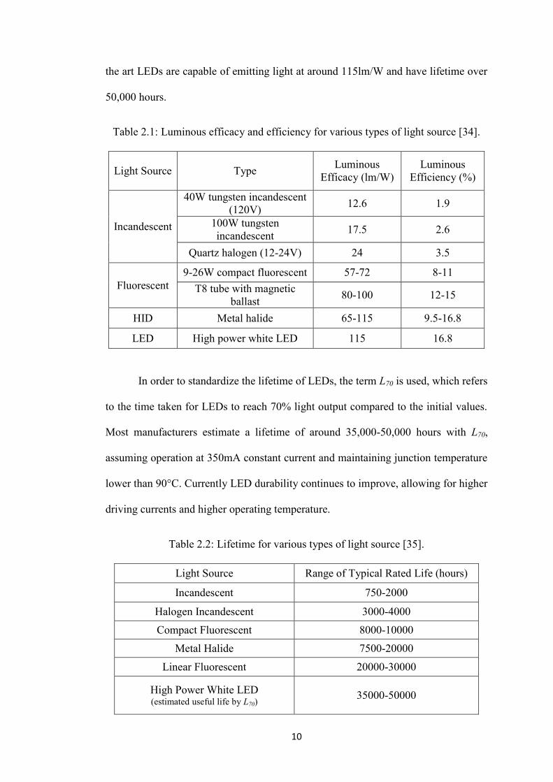
10
the art LEDs are capable of emitting light at around 115lm/W and have lifetime over
50,000 hours.
Table 2.1: Luminous efficacy and efficiency for various types of light source [34].
Light Source Type Luminous
Efficacy (lm/W)
Luminous
Efficiency (%)
Incandescent
40W tungsten incandescent
(120V) 12.6 1.9
100W tungsten
incandescent 17.5 2.6
Quartz halogen (12-24V) 24 3.5
Fluorescent
9-26W compact fluorescent 57-72 8-11
T8 tube with magnetic
ballast 80-100 12-15
HID Metal halide 65-115 9.5-16.8
LED High power white LED 115 16.8
In order to standardize the lifetime of LEDs, the term L70 is used, which refers
to the time taken for LEDs to reach 70% light output compared to the initial values.
Most manufacturers estimate a lifetime of around 35,000-50,000 hours with L70,
assuming operation at 350mA constant current and maintaining junction temperature
lower than 90°C. Currently LED durability continues to improve, allowing for higher
driving currents and higher operating temperature.
Table 2.2: Lifetime for various types of light source [35].
Light Source Range of Typical Rated Life (hours)
Incandescent 750-2000
Halogen Incandescent 3000-4000
Compact Fluorescent 8000-10000
Metal Halide 7500-20000
Linear Fluorescent 20000-30000
High Power White LED (estimated useful life by L70)
35000-50000
11
One of the main applications of modern LEDs is a general light source using
high power white LEDs. These high power LEDs have high efficiency comparable to
fluorescent lamps and very long life time exceeding any other traditional light
sources. As mentioned earlier, it is expected to save $30 billion per year in energy
cost by 2030 by implementing LEDs into a light source. Although the current
application is limited due to their high cost, LEDs will gradually replace other
general light sources over time, saving significant energy and money.
2.3 Theoretical Background of Light Emitting Diodes
LEDs are different from traditional light sources in the way they produce
light. In an incandescent lamp, a tungsten filament is heated by electric current until
it glows and emits light. In a fluorescent lamp, mercury atoms are excited and emit
ultraviolet (UV) radiation. By striking the phosphor coating inside the glass tubes,
the UV radiation is converted and emitted as visible light. In contrast, LEDs are
based on a semiconductor diode [36].
Basic technology of LEDs dates back to the 1960s when scientists were
working with a chip of semiconductor material doped with impurities to create p-n
junction. Useful feature of a p-n junction is that current can flow freely from p to n
direction when p-region has a positive external voltage bias, whereas virtually no
current will flow when p is made negative relative to n. This asymmetry of current
flow makes the p-n junction diode very useful as a rectifier [37].
LEDs which are commonly known as ‘son of diode’ are fabricated by using
wide band gap semiconductors such as GaN or ZnO to form heterostructure or
homostructure devices [38]. Heterojunction LEDs are generated using semiconductor
materials with unequal band gaps whereas homojunction LEDs are fabricated using
same materials with equal band gaps that are differently doped. The main difference
12
between them is that heterojunction LED is brighter than a homojunction LED [39].
Since heterostructure-based LEDs are expected to exhibit improved electronic and
optical confinements compared to homojunction LEDs [40], homojunction structures
have been seldom studied [41].
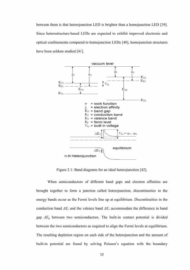
Figure 2.1: Band diagrams for an ideal heterojunction [42].
When semiconductors of different band gaps and electron affinities are
brought together to form a junction called heterojunction, discontinuities in the
energy bands occur as the Fermi levels line up at equilibrium. Discontinuities in the
conduction band ΔEc and the valence band ΔEv accommodate the difference in band
gap ΔEg between two semiconductors. The built-in contact potential is divided
between the two semiconductors as required to align the Fermi levels at equilibrium.
The resulting depletion region on each side of the heterojunction and the amount of
built-in potential are found by solving Poisson’s equation with the boundary
13
condition of continuous electric flux density at the junction. The barrier that electrons
must overcome in moving from the n side to the p side may be quite different from
the barrier for holes moving from p to n. When an electron crosses the barrier and
meets a hole, recombination occurs that will result in spontaneous emission of
photons (light) which is a carrier of electromagnetic radiation of all wavelengths
[43,44].
The actual wavelength and color of light emitted by the LEDs are dependent
on the band gap energy of the materials used to make the p-n heterojunction LEDs.
For examples, red and infrared LEDs are based on aluminum gallium arsenide
(AlGaAs). Blue LEDs are made from indium gallium nitride (InGaN) and green from
aluminum gallium phosphide (AlGaP). White light is created by coating a blue LED
with yellow phosphor, by combining the light from red, green, and blue LEDs or
through the fabrication of heterostructure LED by exploiting the ZnO nanotubes
[45,46].
2.4 Technology of High Power Infrared Emitters
The actual invention of the first practical LED is attributed to Nick Holonyak
in 1962 [47]. He contributed to the development of integrated circuit and was
responsible for the development of p-n-p-n switch which is now widely used as a
dimmer switch to control lighting. In 2004, Mr. Holonyak was officially recognized
as the inventor of LED at a ceremony that was held in Washington [48-50].
Although Nick Holonyak is recognized as the inventor of LED, during 20th
century, several companies either inadvertently or by design were able to generate
electroluminescence from different materials by the application of electric fields. By
the later portion of 1960s, p-n heterojunction devices were fabricated that resulted in
the development of blue LEDs [51]. Although the first generation of blue LEDs were
14
extremely inefficient, subsequent efforts to improve the efficiency of blue SiC LEDs
only marginally improved due to an indirect band gap in the p-n heterojunction
[52,53]. Thus, the low efficiency of SiC LEDs caused scientists turning their
attention to other semiconductor materials both to enhance efficiency as well as to
generate light from other frequency spectrums. One of the approaches was the
discovery of infrared LEDs or commonly known as IREDs or IR emitters based on
the use of GaAs.
During the 1960s, IR emitters were developed based on the use of GaAs that
was grown as a crystal then sliced and polished to form substrate for the epitaxial
growth of p-n hetero`junction diode structures, either by vapor-phase epitaxy or
liquid-phase epitaxy. The use of GaAs resulted in the development of IR emitters
whose application capability was limited owing to the absence of visible light [54-
56].
In 1961, Bob Biard and Gary Pittman were working together on a project for
Texas Instruments to develop gallium arsenide (GaAs) diodes. Using an infrared
microscope, they found that these diodes emitted significant light in the infrared
region. Based on their findings, they received the patent for the IRED, and Texas
Instruments marketed the first commercial LED product [57]. The work of Pittman
and Biard followed intense interest in the properties of semiconductor alloys at
numerous American industrial research labs in the 1950s. For example, Rubin
Braunstein, a physicist at RCA Laboratories in Princeton, NJ (now the David Sarnoff
Research Center), was the first to report on experiments in which he observed light
emission from GaAs and other semiconductor alloys in 1955 [58].
Until 1968, visible and infrared LEDs were extremely costly in the order of
US$200 per unit and so had little practical use. Early in the 20th
century, remote

15
control with the use of IR emitters was one of the most remarkable inventions for
operator convenience as IR region represented a more effective method to control
remotely performed operations [11].
Nowadays, modern IR emitters usually operate in the near IR range in which
light emitted at wavelength from 700-950nm. Today, high power IR emitters are
extensively used in fiber optical communication systems, CCTV, cameras, touch
screen technologies, as well as in the automotive industry such as automatic number
plate recognition, night vision, driver assistance systems, pre-crash sensing systems,
machine vision systems and also as remote control for consumer products [59].
Figure 2.2: Examples of high power IR emitter.
2.5 Concept of Heat Transfer
Heat generation of a solid state lighting device is concentrated in a small
region of the semiconductor die from which it diffuses outward towards the package
where it becomes progressively less concentrated. In other words, the heat flux
density is greatest in the heat generating region of the device. As the energy moves
further and further, heat flux densities are lower and the temperature elevations are
smaller. At the component level, differences in package design, material selection
and quality of manufacture can have enormous impacts on junction operating
temperatures and lifetime of the device. The increase of heat flux densities and the
necessity to control junction temperatures create the need for device characterization.
16
Thermal characterization of a solid state lighting device is the determination
of temperature response of the device junction due to internal self heating, which is a
byproduct of electrical current flow in the device during operation. The heat
generated which elevates the temperature in the semiconductor junctions, conducts
from the junction area through the die towards the package, and eventually dissipates
into the ambient. This flow of heat is governed by the laws of thermodynamics and
the principles of heat transfer. The temperature elevation of the junctions drives the
need for thermal characterization of semiconductor packages since higher junction
temperatures are associated with reduced operating life [60].
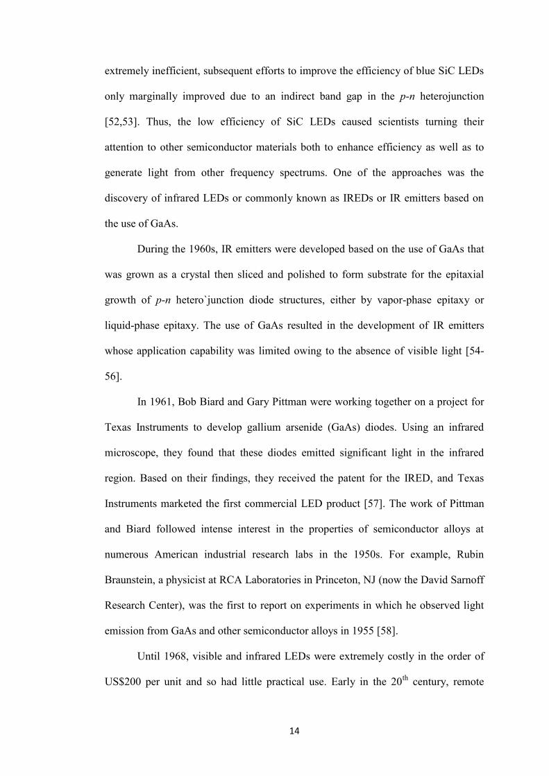
Second Law of Thermodynamics states that heat will flow from a higher
temperature region to a lower temperature region. Once a heat source is attached to
one surface of a component and the opposite surface is kept at a lower ambient
temperature, heat will flow in the direction as indicated in Figure 2.3. The heat will
flow continuously as long as there is a temperature difference [61].
Figure 2.3: Heat flow in a component with temperature difference.
For solid state devices, heat will be generated at the p-n junction once an
active device is in operation. Operating temperature of a device is a result of the
balance between heat generation and heat dissipation. Heat itself does not become a
problem until there is enough heat to cause rise in temperature above critical point.
Basically, heat is flowing from a high temperature region to a region with lower
Heat
Source
Direction of
Heat Flow
Lower Ambient
Temperature

17
temperature by one of the three modes, which are conduction, convection or
radiation.
Conduction is the most effective way to transfer heat among the three, in
which the hot body is in direct contact with the cooler one and heat moves from hot
to cold materials in an attempt to reach equilibrium. The rate of transferring heat
from one to another depends on the temperature gradient, thermal conductivity of the
materials and thickness of the materials.
dx
dTkA
dt
dQ
(1)
This equation is known as the law of heat conduction. dQ/dt is the rate at which heat
flows across the area A, in Joules per second or Watts. dT/dx is the temperature
gradient in degrees Kelvin or Celsius per meter. The thermal conductivity k is a
property of the material [62].
In conjunction with this, convection is a method of transferring heat from a
hot body to a cooler fluid through molecular motion, in which it happens naturally
based on the resulting density gradients caused by temperature variation. In
convection, heat could be carried away faster by forcing the cooling fluid to flow
through the warm body. Conversely, convection heat transfer can be significantly
impeded by device enclosures that restrict air flow, resulting in higher device
temperatures.
Radiation is a removal of heat from a body by the emission of energy in the
form of electromagnetic radiation. It might be in the infrared or even visible parts of
the spectrum depending on the body temperature.

18
2.6 Importance of Thermal Management
High power IR emitters are penetrating fast into lighting applications due to
their improved performance in optical power, efficiency and reliability. However, the
ability to prevent the IR emitters from overheating is the most challenging task for
thermal designers. Hence, an effective thermal management method plays an
important role in the success of solid state lighting devices especially for the high
power IR emitters [63].
Generally, when input current is applied to an IR emitter, only a small portion
of the input power will be emitted as optical power and the rest will be dissipated as
heat from junction to the ambient. As the heat escalates and causes excessive rise in
junction temperature, several key characteristics may become apparent which might
influence and reduce the reliability performance and lifespan. If the thermal
management continues to race out of control, the junction may break down causing a
state of complete thermal runaway. Therefore, thermal management of solid state
lighting devices is becoming more crucial now in order to achieve optimum
performance and longer lifespan especially for high power IR emitters that involve
large amount of power dissipation.
Reliability of an IR emitter is a complex function of the heat generated by the
operation of the IR emitter, the tools used to dissipate heat and the environment in
which the IR emitter is required to operate. Since the demands and applications of
the IR emitters are increasing, diverse thermal management tools have evolved to
help mitigate the issues regarding device reliability. These tools include active
cooling systems, heat sinks, heat pipes and gap fillers.

19
Figure 2.4: Arrhenius equation [63].
Since failure rates, which are described as an Arrhenius equation, increase
exponentially with temperature, a 10°C increase in temperature can double the
failure rate as shown by Figure 2.4. For an operating device where reliability is
critical to success, even 1°C can matter. Thus, the key to improve reliability is to
reduce device temperature by increasing the rate at which heat is dissipated from the
device to the ambient [64].
2.6.1 Metal Core Printed Circuit Board
In conjunction with the rapid progress of solid state lighting industry, board
technology has been extensively examined in order to compensate the need for
thermal management of IR emitters. Printed circuit board (PCB) which consists of
multi-layer structures, plays dual role as electrical circuit connector for developing
electric circuit or arrays of IR emitters and also as heat sink. It was found that 86% of
the heat generated at the p-n junction was dissipated to PCB through conduction
whereas only 14% was dissipated via convection and radiation [65].
Typical FR4 board could not be used because of its low thermal conductivity,
high thermal resistance and it is not capable to meet the continuously increasing
demand on requirement of thermal dissipation for high power IR emitter packages.

20
For more effective thermal management, Metal Core Printed Circuit Board (MCPCB)
should be used [66,67].
Figure 2.5: Internal structure of MCPCB.
MCPCB is composed of a metallic substrate, thin circuit layer with dielectric
material laminated on top, copper layer and a solder layer on top for tinning and
component attachment. The thickness of dielectric layer is usually 100μm as it has
poor thermal conductivity. The metal substrate can be either copper or aluminum. In
most applications, the substrate is attached to a heat sink by using thermal interface
material to provide cooling [68,69].
Compared to conventional FR4 board, the MCPCB provides a better heat
dissipation. MCPCB with a 1W IR emitter can persist at ambient temperature of
around 25oC while the same IR emitter on FR4 board would achieve 12
oC more than
the ambient temperature. Besides, it is one of the simplest ways to provide efficient
cooling to surface mount type electronics. The technology of MCPCB resides in the
dielectric layer, excellent electrical isolation properties and low thermal impedance
[70,71].
Figure 2.6: Examples of MCPCB.
Dielectric Layer
Metallic Substrate (Metal Core)
Copper Circuit Layer
21
The main difference between MCPCB and FR4 board is the thermally
conductive dielectric material in the MCPCB that acts as a thermal bridge between
the components and metal substrate. It was reported that IR emitter soldered on FR4
board tended to radiate more compared to that using MCPCB which conducted heat
in downwards direction for better heat dissipation [72].
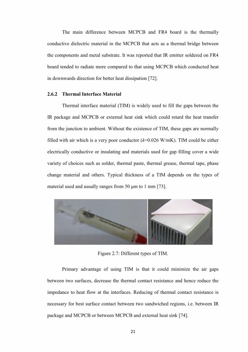
2.6.2 Thermal Interface Material
Thermal interface material (TIM) is widely used to fill the gaps between the
IR package and MCPCB or external heat sink which could retard the heat transfer
from the junction to ambient. Without the existence of TIM, these gaps are normally
filled with air which is a very poor conductor (k=0.026 W/mK). TIM could be either
electrically conductive or insulating and materials used for gap filling cover a wide
variety of choices such as solder, thermal paste, thermal grease, thermal tape, phase
change material and others. Typical thickness of a TIM depends on the types of
material used and usually ranges from 50 μm to 1 mm [73].
Figure 2.7: Different types of TIM.
Primary advantage of using TIM is that it could minimize the air gaps
between two surfaces, decrease the thermal contact resistance and hence reduce the
impedance to heat flow at the interfaces. Reducing of thermal contact resistance is
necessary for best surface contact between two sandwiched regions, i.e. between IR
package and MCPCB or between MCPCB and external heat sink [74].
22
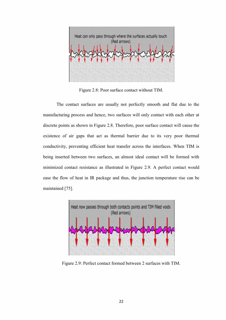
Figure 2.8: Poor surface contact without TIM.
The contact surfaces are usually not perfectly smooth and flat due to the
manufacturing process and hence, two surfaces will only contact with each other at
discrete points as shown in Figure 2.8. Therefore, poor surface contact will cause the
existence of air gaps that act as thermal barrier due to its very poor thermal
conductivity, preventing efficient heat transfer across the interfaces. When TIM is
being inserted between two surfaces, an almost ideal contact will be formed with
minimized contact resistance as illustrated in Figure 2.9. A perfect contact would
ease the flow of heat in IR package and thus, the junction temperature rise can be
maintained [75].
Figure 2.9: Perfect contact formed between 2 surfaces with TIM.
23
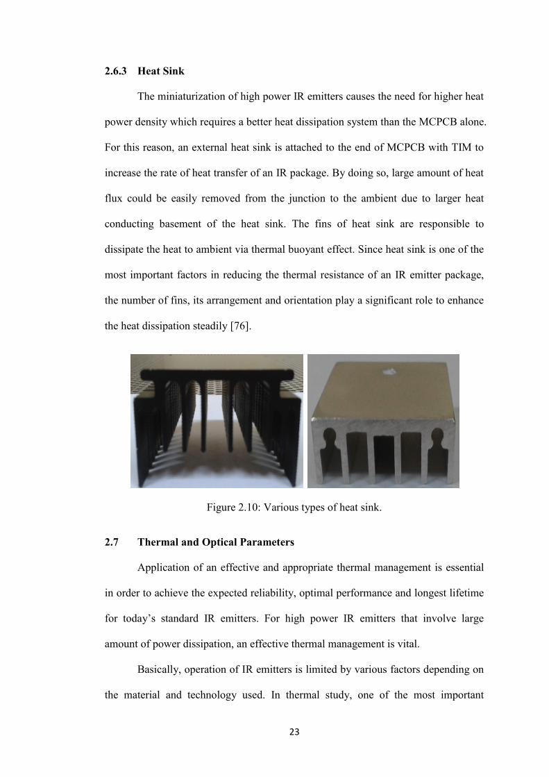
2.6.3 Heat Sink
The miniaturization of high power IR emitters causes the need for higher heat
power density which requires a better heat dissipation system than the MCPCB alone.
For this reason, an external heat sink is attached to the end of MCPCB with TIM to
increase the rate of heat transfer of an IR package. By doing so, large amount of heat
flux could be easily removed from the junction to the ambient due to larger heat
conducting basement of the heat sink. The fins of heat sink are responsible to
dissipate the heat to ambient via thermal buoyant effect. Since heat sink is one of the
most important factors in reducing the thermal resistance of an IR emitter package,
the number of fins, its arrangement and orientation play a significant role to enhance
the heat dissipation steadily [76].
Figure 2.10: Various types of heat sink.
2.7 Thermal and Optical Parameters
Application of an effective and appropriate thermal management is essential
in order to achieve the expected reliability, optimal performance and longest lifetime
for today’s standard IR emitters. For high power IR emitters that involve large
amount of power dissipation, an effective thermal management is vital.
Basically, operation of IR emitters is limited by various factors depending on
the material and technology used. In thermal study, one of the most important
24
parameters with practical interest is the temperature of an active layer for
semiconductor devices or commonly known as junction temperature since it
significantly influences the reliability and durability of IR emitters. Hence, it is
recommended that the maximum junction temperature should not be exceeded during
operation to prevent damage to the IR emitters [77].
Moreover, the main goal in the development of thermal management is to
keep the junction temperature as low as possible. Since thermal resistance is required
to describe the thermal characteristics of the IR emitters independent of the
environment conditions and also it allows the junction temperature to be determined
with sufficient precision, thermal resistance value of the IR emitters is another
important parameter to be studied.
2.7.1 Junction Temperature
Junction temperature is not only a performance indicator but it is one of the
key parameters for solid state lighting devices especially high power IR emitters as
thermal, optical and electrical characteristics of the IR emitters are strongly
dependent on the absolute junction temperature [78].
Junction temperature refers to the temperature of silicon die within the IR
package when the IR emitter is operated or applied with input power. It can also be
referred to as the operating temperature. Junction temperature which is a critical
parameter of the IR emitters affects significantly the internal efficiency, maximum
output power, reliability and other parameters [79]. Thus, low junction temperature
operation is favorable since operating under high temperature will strongly reduce
the overall performance and cause degradation [80].
However, direct junction temperature measurement is not possible due to the
encapsulation and alternative methods must be developed to accurately determine the